

查询PDM41256供应商
PDM41256
256K Static RAM
32K x 8-Bit
1
Features
■ High-speed access times
Com’l: 7, 8, 10, 12, and 15 ns
Ind’l: 8, 10, 12, and 15 ns
■ Low power operation (typical)
- PDM41256SA
Active: 400 mW
Standby: 150 mW
- PDM41256LA
Active: 350 mW
Standby: 25 mW
■ Single +5V (±10%) power supply
■ TTL-compatible inputs and outputs
■ Packages
Plastic SOJ (300 mil) - TSO
Plastic TSOP - T
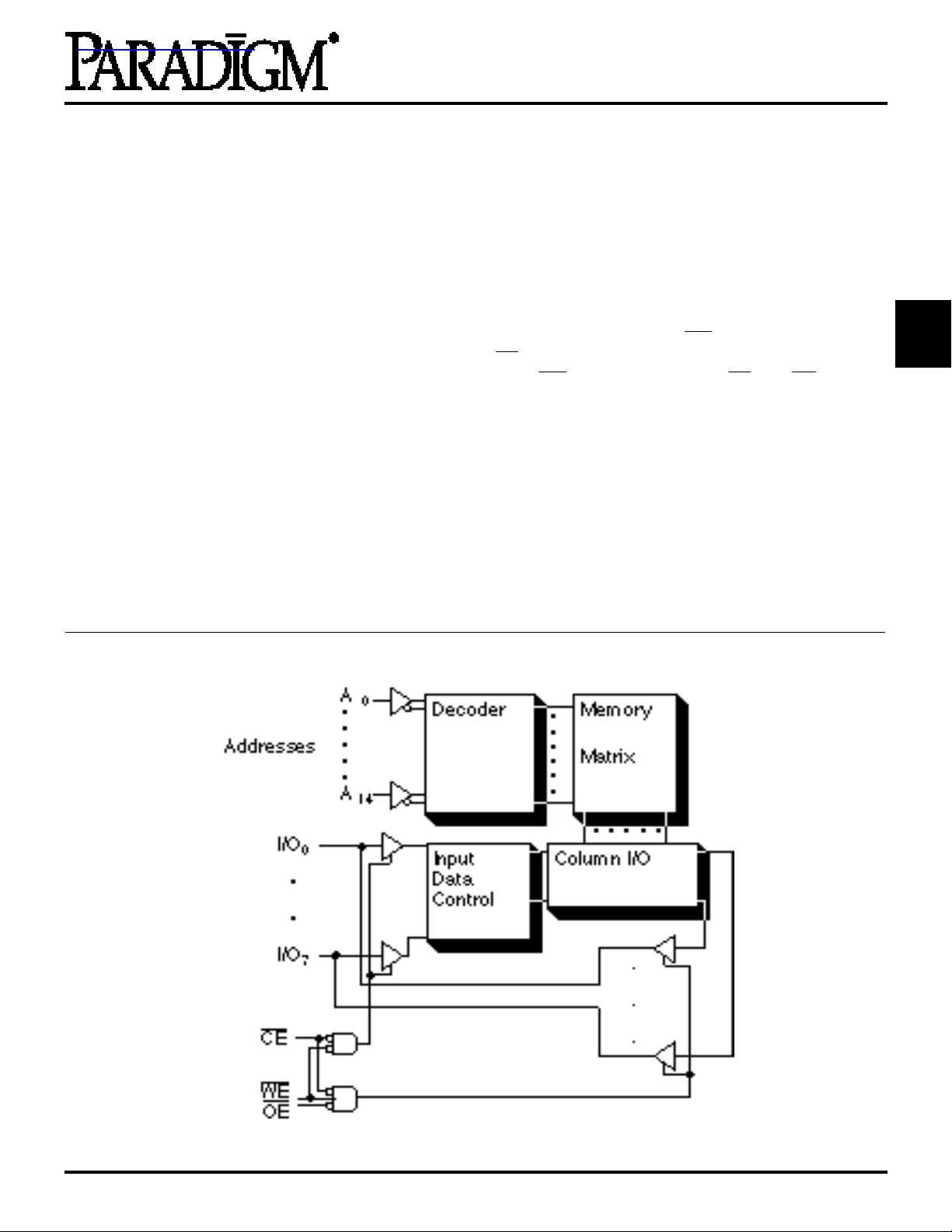
Functional Block Diagram
Description
The PDM41256 is a high-performance CMOS static
RAM organized as 32,768 x 8 bits. This product is
produced in Paradigm’s proprietary CMOS
technology which offers the designer the highest
speed parts. Writing to this device is accomplished
when the write enable (WE) and the chip enable
(CE) inputs are both LOW. Reading is accomplished
when WE remains HIGH and CE and OE are both
LOW.
The PDM41256 operates from a single +5V power
supply and all the inputs and outputs are fully TTLcompatible. The PDM41256 comes in two versions,
the standard power version PDM41256SA and a low
power version the PDM41256LA. The two versions
are functionally the same and only differ in their
power consumption.
The PDM41256 is available in a 28-pin plastic TSOP
and a 28-pin 300-mil plastic SOJ.
2
3
4
5
6
7
Rev. 2.0 - 7/17/96 3-33
8
9
10
11
12
PDM41256
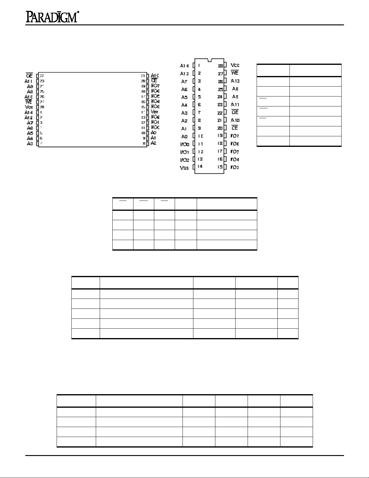
Pin Configurations
TSOP
SOJ
Truth Table
OE WE CE I/O MODE
X X H Hi-Z Standby
L H L D
X L L D
H H L Hi-Z Output Disable
OUT
IN
Read
Write
Pin Description
Name Description
A14-A0 Address Inputs
I/O7-I/O0 Data Inputs/Outputs
OE Output Enable Input
WE Write Enable Input
CE Chip Enable Input
V
CC
V
SS
Power (+5V)
Ground
NOTE: 1. H = VIH, L = VIL, X = DON’T CARE
Absolute Maximum Ratings
Symbol Rating Com’l. Ind. Unit
V
T
T
P
I
OUT
TERM
BIAS
STG
T
Terminal Voltage with Respect to Vss –0.5 to +7.0 –0.5 to +7.0 V
Temperature Under Bias –55 to +125 –65 to +135 °C
Storage Temperature –55 to +125 –65 to +150 °C
Power Dissipation 1.0 1.0 W
DC Output Current 50 50 mA
(1)
NOTE: 1. Stresses greater than those listed under ABSOLUTE MAXIMUM RATINGS may
cause permanent damage to the device. This is a stress rating only and functional
operation of the device at these or any other conditions above those indicated in the
operational sections of this specification is not implied. Exposure to absolute maximum rating conditions for extended periods may affect reliability.
Recommended DC Operating Conditions
Symbol Parameter Min. Typ. Max. Unit
V
CC
V
SS
Commercial Ambient Temperature 0 25 70 °C
Industrial Ambient Temperature –40 25 85 °C
Supply Voltage 4.5 5.0 5.5 V
Supply Voltage 0 0 0 V
3-34 Rev. 2.0 - 7/17/96
PDM41256
DC Electrical Characteristics (V
Symbol Parameter Test Conditions Min. Max. Min. Max.
I
LI
I
LO
V
IL
V
IH
V
OL
V
OH
NOTE: 1. VIL(min) = –3.0V for pulse width less than 20 ns.
Input Leakage Current VCC = MAX., VIN = Vss to V
Output Leakage Current VCC= MAX.,
Input Low Voltage –0.5
Input High Voltage 2.2 6.0 2.2 6.0 V
Output Low Voltage IOL=8 mA, VCC = Min.
Output High Voltage IOH = –4 mA, VCC = Min. 2.4 — 2.4 — V
= 5.0V ± 10%)
CC
CE = VIH, V
IOL = 10 mA, VCC = Min.
= Vss to V
OUT
CC
CC
Com’l/
Ind.
Com’l/
Ind.
PSM41256SA PSM41256LA Unit
–5 5 –5 5 µA
–5 5 –5 5 µA
—
—
(1)
0.8 –0.5
0.4
0.5
(1)
—
—
Power Supply Characteristics
-7 -8 -10 -12 -15
Symbol Parameter Power Com’l. Com’l. Ind. Com’l. Ind. Com’l. Ind. Com’l. Ind. Units
I
CC
I
SB
I
SB1
Operating Current
CE = V
IL
f = f
= 1/t
MAX
VCC = Max
I
= 0 mA
OUT
Standby Current
CE = VIH
f = f
MAX
VCC = Max
Full Standby Current
CE ≥ VCC – 0.2V
f = 0
VCC = Max
VIN ≥ VCC – 0.2V or ≤ 0.2V
= 1/t
RC
RC
SA 210 200 210 190 200 180 190 170 180 mA
LA 190 180 190 170 180 160 170 150 160 mA
SA 90 80 80 70 70 60 60 50 50 mA
LA 90 80 80 70 70 60 60 50 50 mA
SA 20 20 20 20 20 20 20 20 20 mA
LA 5 5 10 5 10 5 10 5 10 mA
0.8 V
0.4
0.5
1
2
V
3
4
5
6
7
8
SHADED AREA = PRELIMINARY DATA
NOTE:All values are maximum guaranteed values.
Capacitance
Symbol Parameter Max. Unit
C
IN
C
OUT
NOTE: 1. This parameter is determined by device characterization but is not production
tested.
Rev. 2.0 - 7/17/96 3-35
(1)
(T
= +25°C, f = 1.0 MHz)
A
Input Capacitance 8 pF
Output Capacitance 8 pF
9
10
11
12

AC Test Conditions
Input pulse levels VSS to 3.0V
Input rise and fall times 3 ns
Input timing reference levels 1.5V
Output reference levels 1.5V
Output load See Figures 1 and 2
PDM41256
Figure 1. Output Load Equivalent Figure 2. Output Load Equivalent
(for t
Figure 3.
LZCE
, t
HZCE
, t
t
HZOE
LZWE
, t
, t
HZWE
)
LZOE
,
3-36 Rev. 2.0 - 7/17/96

PDM41256
Read Cycle No. 1
Read Cycle No. 2
(1)
1
2
3
(2)
4
5
AC Electrical Characteristics
Description --7
READ Cycle Sym Min. Max. Min. Max. Min. Max. Min. Max. Min. Max. Units
READ cycle time t
Address access time t
Chip enable access time t
Output hold from address change t
Chip enable to output in low Z
Chip disable to output in high Z
Chip enable to power up time
Chip disable to power down time
Output enable access time t
Output enable to output in low Z
Output disable to output in high Z
SHADED AREA = PRELIMINARY DATA.
Notes referenced are after Data Retention Table.
(3, 4, 5)
(3, 4, 5)
(4)
(4)
(4, 5)
(4, 5)
RC
AA
ACE
OH
t
LZCE
t
HZCE
t
PU
t
PD
AOE
t
LZOE
t
HZOE
(6)
7 8 10 12 15 ns
7 8 10 12 15 ns
7 8 10 12 15 ns
3 3 3 3 3 ns
5 5 5 5 5 ns
5 6 6 6 6 ns
0 0 0 0 0 ns
7 8 10 12 15 ns
5 5 5 6 8 ns
0 0 0 0 0 ns
5 6 6 6 6 ns
--8
(6)
-10
(6)
-12 -15
6
7
8
9
10
11
12
Rev. 2.0 - 7/17/96 3-37

Write Cycle No. 1 (Write Enable Controlled)
Write Cycle No. 2 (Chip Enable Controlled)
PDM41256
AC Electrical Characteristics
Description -7
(6)
WRITE Cycle Sym Min. Max. Min. Max. Min. Max. Min. Max. Min. Max. Units
WRITE cycle time t
Chip enable to end of write t
Address valid to end of write t
Address setup time t
Address hold from end of write t
Write pulse width t
Data setup time t
Data hold time t
Write disable to output in low Z
Write enable to output in high Z
(4, 5)
(4, 5)
WC
CW
AW
WP
t
LZWE
t
HZWE
7 8 10 12 15 ns
7 8 10 10 12 ns
7 8 10 10 12 ns
0 0 0 0 0 ns
AS
0 0 0 0 0 ns
AH
7 8 10 10 11 ns
6 7 7 7 7 ns
DS
0 0 0 0 0 ns
DH
0 0 0 0 0 ns
3 3 3 3 3 ns
SHADED AREA = PRELIMINARY DATA.
3-38 Rev. 2.0 - 7/17/96
(6)
-8
-10
(6)
-12 -15

Low VCC Data Retention Waveform
PDM41256
1
2
3
Data Retention Electrical Characteristics (LA Version Only)
Symbol Parameter Test Conditions Min. Typ. Max. Unit
V
I
CCDR
t
CDR
t
NOTES: (For three previous Electrical Characteristics tables)
VCC for Retention Data 2 — — V
DR
Data Retention Current CE ≥ VCC – 0.2V
VIN ≥ VCC – 0.2V
or ≤ 0.2V
Chip Deselect to Data Retention Time 0 — — ns
(4)
Operation Recovery Time t
R
1. The device is continuously selected. Chip Enable is held in its active state.
2. The address is valid prior to or coincident with the latest occuring Chip Enable.
3. At any given temperature and voltage condition, t
4. This parameter is sampled.
5. The parameter is tested with CL = 5 pF as shown in Figure 2. Transition is measured ±200 mV from steady state voltage
6. Vcc = 5V ± 5%.
is less than t
HZCE
VCC = 2V — 95 500 µA
VCC = 3V — 350 750 µA
— — ns
LZCE
RC
.
4
5
6
7
8
9
Rev. 2.0 - 7/17/96 3-39
10
11
12

Ordering Information
PDM41256
3-40 Rev. 2.0 - 7/17/96
 Loading...