

Page 1

PG-3210 Service Manual PG-3210
PG-3210 Service Manual
(GSM Cellular Phone)
Pantech Co., Ltd., Korea
February 22, 2005
1st Edition
For Use by Authorized Service/Maintenance Personal Only
Documents to Receive This Addendum:
PG-3210 Maintenance/Repair/Operating Manual
Page 2

PG-3210 Service Manual
1
PANTECH
CONTENTS
SECTION 1 INTRODUCTION .............................................................................................................3
1.1 INTRODUCTION ..............................................................................................................................3
1.2 FREQUENCY ALLOCATION AND ITS USE ...........................................................................................3
1.3 ITEM NAME AND USE...................................................................................................................... 4
1.4 CHARACTERISTICS.........................................................................................................................4
SECTION 2 ELECTRICAL SPECIFICATIONS....................................................................................5
2.1 GENERAL ......................................................................................................................................5
2.2 TRANSMITTER…………………………………………………………………………………………….5
2.3 RECEIVER…………………………………………………………………………………………………5
SECTION 3 OPERATION....................................................................................................................6
3.1 NAME OF EACH PART…..……………………………….…………………………………………………6
3.2.DISPLAY ..………………….…………………………….………………………………………………..7
3.3 KEYPAD …………………………………….………….………………………………………………..7
3.4 CAMERA MODULE
SECTION 4 THEORY OF OPERATION..............................................................................................8
4.1 LOGIC SECTION........................................................................................................................8
4.1.1 DC DISTRIBUTION AND REGULATION PART…………………………………………………………….8
4.1.2 LOGIC PART…………………………………………………………………………………………….8
4.1.2.1 SUMMARY…………………………………………………………………………………………….8
4.1.2.2 BASEBAND DIGITAL SIGNAL PROCESSING…………………………………………………………..8
4.1.3 MEMORY PART………………………………………………………………………………………..10
4.1.4 NOTIFICATION PART.................................................................................................................. 11
4.1.5 KEY PAD PART..........................................................................................................................11
4.1.6 LCD MODULE(DISPLAY PART)................................................................................................... 11
4.1.7 CAMERA MODULE
4.2 RADIO TRANSCEIVER SECTION.....................................................................................................12
4.2.1 DC DISTRIBUTION AND REGULATION PART ................................................................................. 13
4.2.3 RECEIVE SECTION………………………………………………………………………………….…14
4.2.3.1 AN OVERVIEW OF RECEIVE SECTION.......................................................................................17
4.2.3.2 RECEIVER PART……………………………………………………………………………….……18
4.2.4 TRANSMIT SECTION ..................................................................................................................19
4.2.4.1 AN OVERVIEW OF TRANSMIT SECTION ....................................................................................19
4.2.4.2 TRANSMITTER PART...............................................................................................................20
4.2.5 OFFSET PLL……………………………………………………………………………….…………..21
4.2.5.1 AN OVERVIEW OF OFFSET PLL............................................................................................21
4.2.5.2 VCTCXO(VOLTAGE CONTROLLED TEMPERATURE COMPENSATED CRYSTAL OSCILLATOR):V801….22
SECTION 5 ALIGNMENT PROCEDURE..........................................................................................23
5.1 RECOMMENDED TEST EQUIPMENT................................................................................................23
5.2 CONNECTION OF TEST EQUIPMENT...............................................................................................23
SECTION 6 EQUIPMENT REPAIR PROCEDURE...........................................................................24
6.1 NO POWER ON WITH BATTERY APPLIED ..........................................................................................24
6.1.1 POWER CHECK.........................................................................................................................24
6.1.2 OSCILLATION CHECK ................................................................................................................30
6.1.3 KEYPAD LED NOT IN OPERATION(3-COLOR AND BLUE) ..............................................................31
6.1.4 LCD EL BACKLIGHT LED NOT IN OPERATION(WHITE)..………………………………………… …33
6.2 AUDIO PART(EARPIECE, HANDS FREE EARPHONE, MICROPHONE, HANDS FREE MIC) ..................35
6.2.1 NO RECEIVING TONE HEARD (EARPIECE) ..................................................................................35
6.2.2 NO RECEIVING TONE HEARD (HANDS FREE EARPHONE).............................................................35
6.2.3 SIDETONE NOT TRANSMITTED (EARPIECE)................................................................................38
6.2.4 SIDETONE NOT TRANSMITTED (HANDS FREE MIC) .....................................................................38
6.2.5 HOOK SWITCH NOT WORKING ..................................................................................................39
Page 3

PG-3210 Service Manual
1
PANTECH
6.2.6 MELODY NOT RINGING.............................................................................................................40
6.2.7 VIBRATOR NOT WORKING …………………………………………………………………...…41
6.3 SIM CARD PART ……………………………………...…………………………………………….42
6.3.1 SIM ERROR ………………………………………………………………………………………….42
6.4 CHARGER PART……………………………………………………………………………………..43
6.4.1 CHARGING ERROR ………………………………..…………………………………………………43
6.5 RF PART…………….………………………………………………………………………………… 45
6.5.1 TEST CONDITIONS………………………………………………………………… …………………45
6.5.2 POWER SUPPLY CHECK POINT……………………………………………………………………….46
6.5.3 POWER AMPLIFIER MODULE ………………………………………………………………………...48
6.5.4 VCTCXO...…………...………………………………………………………………………………..50
6.5.5 FRONT END MODULE……………………………………………………….…………………..51
Page 4

PG-3210 Service Manual
1
PANTECH
SECTION 1. Introduction
1.1 An Introduction of GSM Digital Cellular Mobile Communication System
GSM (Global System for Mobile communication) concluded that digital technology working in
the Time Division Multiple Access (TDMA) mode would provide the optimum solution for the
future system. Specifically , a TDMA system has the following advantage
► Offers a possibility of channel splitting and advanced speech coding ,resulting in improved
spectrum efficiency.
► Offers much greater variety of service than the analog
► Allows considerable improvements to be made with regards to the protection of information.
The GSM system is basically designed as a combination of three major subsystem;
The network subsystem, the radio subsystem, and the operation support system.
The functional architecture of a GSM system can be divided into the Mobile Station (MS), the Base
Station (BS), and the Network Subsystem (NS). The MS is carried by the subscriber, the BS
subsystem controls the radio link with the MS and the NS performs the switching of calls between
the mobile and other fixed or mobile network users as well as mobility management. The MS and
the BS subsystem communicate across the Um interface also known as radio link
The specifications relating to MS are as follows:
z TS 100 607-1 : Digital cellular telecommunication system(Phase2+)Mobile Station (MS)
Conformance specification Part1:Conformance specification
1.2 Frequency Allocation and Its Use
z Transmit frequency band : 824MHz ~ 849MHz(For GSM850) , 1710MHz ~1785MHz(For DCS),
1850MHz ~1910MHz(For PCS)
z Receive frequency band: 869MHz ~ 894MHz(For GSM850), 1805MHz ~ 1880MHz(For DCS),
1930MHz ~ 1990MHz(For PCS)
z Channel spacing : 200 KHz
z ARFCN(Absolute Radio Frequency Channel Number) : 128~251 (For GSM850), 512~885 ( For
DCS), 512~810 (For PCS)
z Transmit-receive frequency spacing: 45 MHz(For GSM850), 95MHz(For DCS), 80MHz(For
PCS)
z Frequency band and Channel Arrangement
For GSM850 Band Fl(n)=824.2+0.2*(n-128) 128 ≤n≤ 251 Fu(n)=Fl(n)+45
824 MHz ~849 MHz : Mobile Transmit,Base receive
869 MHz ~894 MHz : Base Transmit, Mobile receive
For DCS Fl(n)=1710.2+0.2*(n-512) 512≤n≤885 Fu(n)=Fl(n)+95
1710 MHz ~ 1785 MHz : Mobile Transmit,Base receive
1805 MHz ~ 1880 MHz : Base Transmit, Mobile receive
For PCS Band Fl(n)=1850.2+0.2*(n-512) 512 ≤n≤ 810 Fu(n)=Fl(n)+80
1850 MHz ~1910 MHz : Mobile Transmit,Base receive
Page 5

PG-3210 Service Manual
1
PANTECH
1930 MHz ~1990 MHz : Base Transmit, Mobile receive
** Fl(n)= frequency value of the carrier , Fu(n)= corresponding frequency value in upper band
1.3 Item Name and Usage
PG-3210, GSM digital cell phone, is supercompact, superlight mobile communication terminal for
personal use. It has a 850MHz, 1800MHz and 1900MHz frequency band and adopts GSM850,
DCS and PCS mode having excellent spectrum efficiency, economy, and portability.
This product is GSM Cellular type portable phone, adopting 1-cell Li-ion battery and power saving
circuit to maximize its operation time. Also, it is equipped with a fixed snap-in antenna and its color
LCD with font built in enables both Chinese and English text service. And power control(basic
feature of GSM), security feature, voice symbol feature, and variable data rate feature are used
appropriately to ensure its best performance. This product consists of a handset, battery pack, and
travel charger.
1.4 Characteristics
1) All the active devices of PG-3210 are made of semiconductors to ensure excellent performance
and semi-permanent use.
2) Surface mounting device (SMD) is used to ensure high reliability, compactness and lightness.
3) PG-3210 adopts the Silab’s Aero II RF transceiver, which is a complete RF front end for
multi-band GSM and GPRS wireless communications.
4) PG-3210 is designed to perform excellently even in the worst environment
Page 6

PG-3210 Service Manual
1
PANTECH
Section 2. Electrical Specifications
2.1 General GSM850 / DCS / PCS Band
Mobile Transmit Frequency
824MHz~849MHz / 1710MHz ~ 1785MHz / 1850MHz
~1910MHz
Mobile Receive Frequency
869MHz~894MHz / 1805MHz~1880MHz / 1930MHz
~1990MHz
The Number of Time Slot 8
The Number of Channels 124 / 374 / 299
Channel Spacing 200 kHz
Power Supply Rechargeable Li-Ion Battery 3.7V/730mAH(850mAH)
Operating Temperature -10℃ ∼ +55℃
Dimension 69(H) ×43(W) ×18.35(D) mm (SLIM)
Weight About 71 g
2.2 Transmitter GSM850 / DCS / PCS Band
Maximum Output Power 33±2 / 30±2 / 30±2dBm
Frequency Error ±90Hz / ±180Hz
Phase Error RMS < 5°, PEAK < 20°
Minimum Output Power 5±5 / 0±5 / 0±5dBm
Power Control 5~19 / 0~15 / 0~15 (2 dB Step)
Output RF Spectrum TS 100 910V6.2.0
Switching Transient TS 100 910V6.2.0
Intermodulation attenuation TS 100 910V6.2.0
Idle Mode
-57dBm 9KHz~824M / 849MHz~1GHz
-59dBm 824MHz~849MHz
-53dBm 1.85~1.91GHz
-47dBm 1~1.85GHz / 1.91GHz~12.75GHz
Conducted Spurious Emissions
Allocated Channel
-36dBm 9KHz~ 1GHz
-30dBm 1GHz~ 12.75GHz
2.3 Receiver
Reference Sensitivity -102dBm
C/Ic 9 dB
C/Ia1 -9 dB
C/Ia2 -41 dB
For Adjacent interference
For Adjacent(200KHz) interference
For Adjacent(400KHz) interference
For Adjacent(600KHz) interference
C/Ia3 -49 dB
Page 7
PG-3210 Service Manual
1
PANTECH
Section 3 Operation
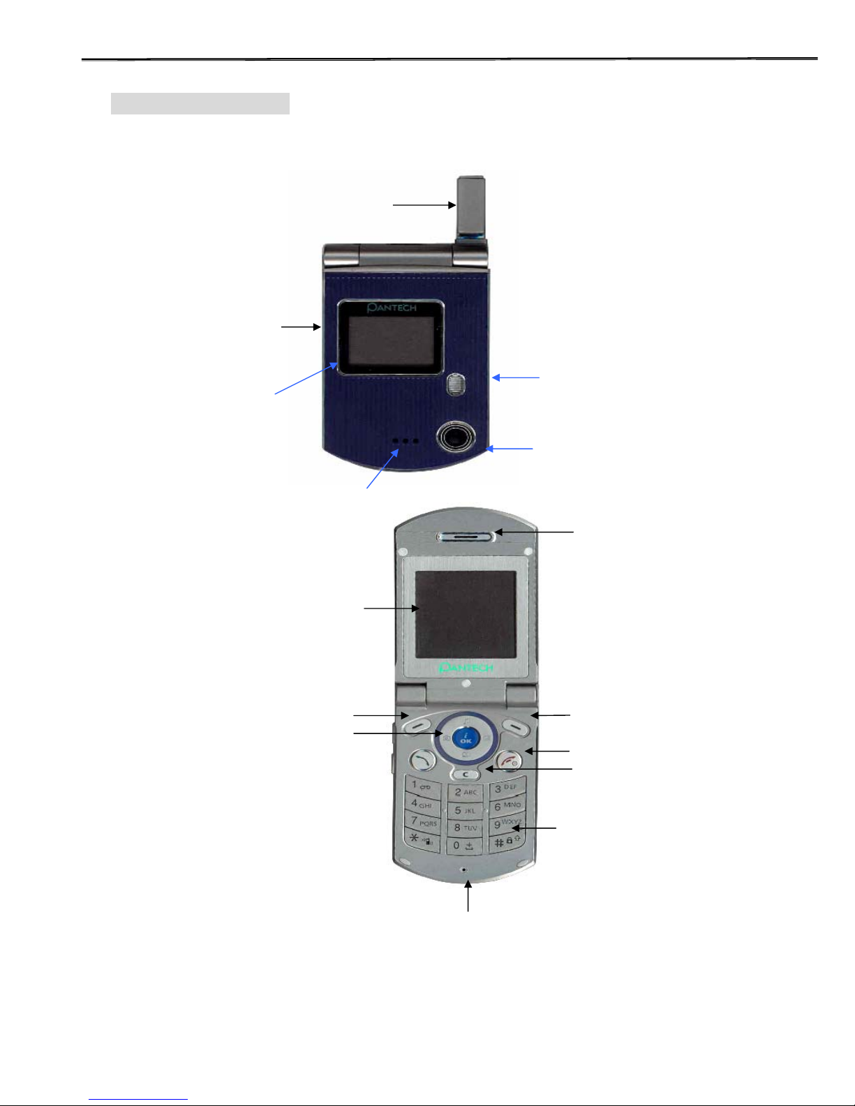
3.1 Name of each part
Stub PCB Antenna
(Body color)
330K CCD
Camera
SPK Hall
1.0’ 260K TFT
(96x64 pixels)
V olume
up/down
1.52’ 260K TFT
(128*128
pixels)
Soft Key 1
5 Way Menu
Navigation Key
Upper : Profile
Right: Message
Down :Camera
Left: Favorite
Center: W AP & OK
Soft Key 2
Numeric
Keypad
End/
MIC Hall
Receiver Hall
Clear Key
Page 8

PG-3210 Service Manual
1
PANTECH
3.2 Display(Dual LCD)
Parameter Projected Actual(MAIN LCD)
Display Color TFT LCD with white LED back lighting
1.52” 260k colors
Pixels : 128*128 pixels
Character : (font size : 12/14/16) 8characters x 8lines(max)
Driver TP042(TOPPOLY)
Module Dimen. 37.2(W) x 40.1(H) x 4.05(D) mm
Effective Area 27.26(W) x 27.27(H) mm (1.5 inch)
Number of Pixel 128(W) x RGB(W)x 128(H) pixel
Pixel pitch 71(W) x 213(H) um
Parameter Projected Actual(SUB LCD)
Display Color TFT LCD with white LED back lighting
1.0” 260k colors
Pixels : 96 x 64
Character : 6characters x 4lines(max)
Module Dimen. 37.2(W) x 40.1(H) x 4.05(D) mm
Effective Area 21.02(W) x 14.02(H) mm (1.0 inch)
Number of Pixel 96(W) x RGB(W) x 64(H) pixel
Pixel pitch 73(W) x 219(H) um
3.3 Keypad
Market Goal Projected Actual Comments
English
Keypad
0-9, *,#
Send (Color)
End/Pwr (Color)
Up, Down, WAP
Soft1, Soft2, CLR
Camera
* Key: Vib. Mode
# Key: Auto Lock
0/+Key: nternational
2 Volume Keys
0-9, *,#
Send (Color)
End/Pwr (Color)
Up, Down, WAP
Soft1, Soft2, CLR
Camera
* Key: Vib. Mode
# Key: Auto Lock
0/+ Key: International
2 Volume Keys
Meets Goal.
(Industrial
design sample
required)
Meets Goal
Keys for VR and
Lock
International
Volume
up/down
3.4.Camera Module
Product Name
IGT99268B-P40(SANYO)
Effective pixel array 640 x 480
Unit Pixel size 3.3um x 3.3um
Module size 8.0mm x 8.0mm x 5.0mm
Operating voltage 2.9V
Weight 0.5g or below
Page 9

PG-3210 Service Manual
1
PANTECH
Section 4. Theory of Operation
4.1 Logic Section
4.1.1 DC Distribution and Regulation Part
Applying battery voltage and pressing “END” key on the key pad short-circuits “Ground” and “
PowerON”. AD6537B(U102) control that power manage regarding power on/off in handset
Pressing POWERKEY on the key pad is active on the handset.
This will turn on all the LDOs, when PowerON is held low. The power of RF Tx power amplifier is
supplied directly by the battery.
4.1.2 Logic part
4.1.2.1 Summary
The logic part consists of AD6527 ARM7 microprocessor-combined DBB(Digital BaseBand)
GSM-ASIC, COMBO(flash ROM & SRAM), AD6537B ABB(Analog BaseBand) Chip. AD6527 is
GSM-ASIC chipset implemented for GSM terminal’s system control and baseband digital signal
processing.
Major parts used in the logic part are as follows:
1) AD6527 : U101, [ARM7 Processor Core + DBB GSM Signal Processing] ASIC
2) AD6537B : U102, Analog Baseband Processor (Power management + Voice Codec)
3) COMBO MEMORY(Flash ROM : U103, 128Mbit Flash Memory + 32Mbit SRAM )
4.1.2.2 Baseband Digital Signal Processing
AD6527 is a GSM core device containing ARM7 CPU core. AD6527 is 204 pin LFBGA (mini-BGA)
package, consisting of terminal chips. The function and characteristics of clock are as follows:
1) Complete single chip GSM Processor
2) Channel codec sub-system
• Channel coder and decoder
• Interleaver and Deinterleaver
• Encryption and Decryption
3) Control Processor Subsystem including
• Parallel and serial Display interface
• Keypad Interface
• SIM Interface
• Control of RADIO subsystem
• Real Time Clock with Alarm
Page 10

PG-3210 Service Manual
1
PANTECH
☞ Configuration by Function of AD6527
1 Microprocessor Core
AD6527 has a built-in ARM7 microprocessor core, including microprocessor interrupt controller,
timer/counter, and DMA controller. And besides, 32bit data path is included, and up to 8Mbyte
addressing is enabled and can be extended up to 16Mbyte. Although external clock should be
provided to operate the microprocessor, this core uses 13MHz VCTCXO to provide clock.
2 Input Clock
1) Main Clock(13 MHz):
This is the clock needed for the microprocessor built in AD6527 to operate.
2) VC-TCXO(26 MHz) , 32.768KHz Clock:
This is the system reference clock to control SLEEP mode.
This is the clock derived from 26MHz VC-TCXO clock, provided by RF part. It is the timing
reference clock for GSM signal processing.
3 DSP Subsystem
This is a GSM signal processing part in GSM mode, consisting of speech transcoding and
Channel equalization as follows:
1) Speech transcoding
In full rate, the DSP receives the speech data stream from VBC and encodes data from 104kbps to
13kbps. Using algorithm is Regular Pulse Excitation with Long Term Prediction (RPE-LTP).
2) Equalization
The Equalizer recovers and demodulates the received signal
The Equalizer establishes local timing and frequency references for mobile terminal as well as
RSSI calculation.
The equlization algorithm is a version of Maximum Likelihood Sequency Estimation(MLSI)
using Viterbi Algorithm.
☞ GSM Core and RF Interface
1) Transmitter:
AD6537B ABB receive data at 270kbps and use an on chip lock-up table to perform GMSK
modulation. A pair of 10bit matched differential DACs convert the modulated data and pass
I and Q analog data to the transmit section of the radio system.
2) Receiver:
The receiver I and Q signals are sampled by a pair of ADCs at 270kbps.
The I and Q samples are transferred to the ABB through a dedicated receive path serial port.
Page 11

PG-3210 Service Manual
1
PANTECH
4 RF Interface
This interfaces the RF part to control power amplifier, Tx LO buffer amplifier, VC-TCXO, and
AGC-end on transmit/receive paths in the RF part.
1) Transmitter Interface:
This sends Ramp_DAC signal to the RF part to control power amplifier.
2) Receiver Interface:
This transmits RX_AGC signal to Rx AGC amp. to adjust receive path gain.
5 General Purpose ADC Support
The AD6537B includes a general purpose 10bit auxiliary ADC with four multiplexed input channel
These are used for measurment of battery voltage ID , temperature and accessory ID.
6 USC(Universal System Connector) Interface
A Typical GSM handset requires serial connections to provide data during normal phone operation
manufacturing,testing and debugging.
7 General Purpose Interface
The AD6527 provides 32 interface pin for control of peripheral devices.
All GPIO pins start up as inputs. Additional purpose inputs and outputs are available under SW
control.
8 Speech Transcoding
In full rate mode, the DSP receive the speech data stream from the ABB and encodes data from
104kbps to 13kbps.Using algorithm is Regular Pulse Exitation with Long Term Prediction as
specified GSM Recommandation
9 Power Down Control Section
1) Idle Mode Control:
If IDLE/ signal turns ‘Low’, transmitter section becomes disabled.
2) Sleep Mode Control:
If IDLE/ and SLEEP/ signals turn ‘Low’, all the sections except for VC-TCXO circuit become
disabled.
3) Receiver & Transmitter Mode Control:
If IDLE/ and SLEEP/ signals turn ‘High’, all the sections become enabled to perform
transmit/receive operation.
4.1.3 Memory Part
Memory consists of COMBO (flash ROM & SRAM).
1 Flash ROM
Flash ROM has a capacity of 128Mbit(16MByte). The main programs of the terminal(call processing,
user interface, and diagnostic task) and supplemental programs (NAM program and test program)
are stored in the flash ROM. Even if the program version may be changed in the future, customers
can download the program.
2 Static RAM
Page 12

PG-3210 Service Manual
1
PANTECH
SRAM has a capacity of 32Mbit(4MByte) and stores system parameters, data buffer, and stack of
each task in it.
3 Key Tone Generation
All alert signals are generated by the DSP and output to the ABB audio output.
These alert can be used for the earpiece.
4.1.4 Notification Part
The notification of incoming call is given by melody, vibrator.
1) Melody:
This is a device sounding alert/melody tones.
The melody datas are stored in flash memory (U103) And generated by Melody IC(U104).
2) Vibrator:
This is a device enabling vibration. The vibrator data is stored in flash memory(U103)
And generated by A10(GPIO_9)pin.
4.1.5 Key Pad Part
To enable key operation to input information, the key matrix is configured using strobe signal of
KEYPADROW(0-4) and 5 input ports of KEYPADCOL(0-4). Also, to use the key even at light, the
backlight circuit is provided for LED 16s.
4.1.6 LCD Module(Display Part)
LCD module consists of LCD, controller, LED-Backlight,
LCD: 1S/W Icon x 1 lines[(128x3)x128] can be displayed on the LCD panel. 6 icons could be
provided by S/W. Controller with English font built in has been used.
LED-backlight Using illuminates the LCD panel, and LCD reflector enhances LCD display effect.
4.1.7 CAMERA Module
Camera Module is activated by keypad sw105.
Taking a picture, Flash LED is provided to bright dark surroundings, and generated by
U101.P16(GPO18)
Page 13
PG-3210 Service Manual
1
PANTECH
4.2 Radio Transceiver Section
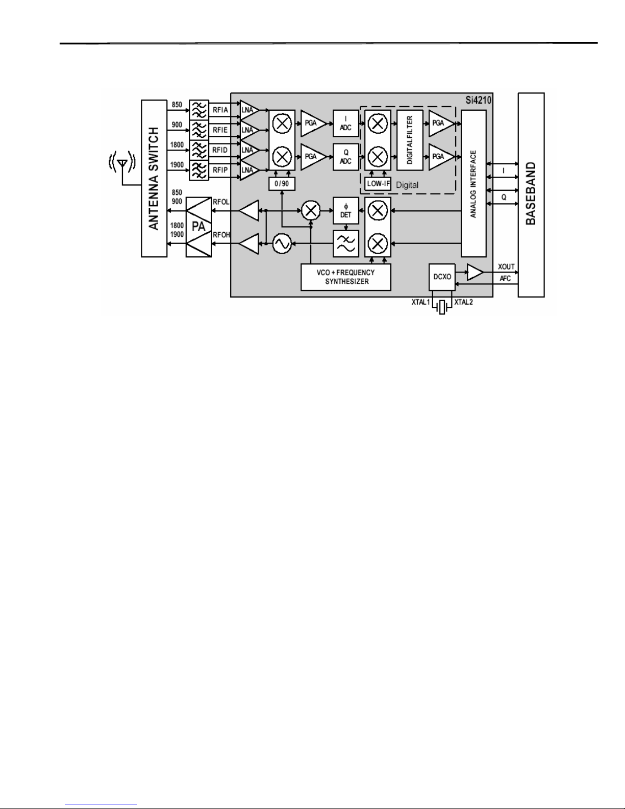
Fig.4-1. RF Transceiver block diagram
The PG-3210’s RF Transceiver, which is Aero II, is the industry's most integrated RF front end for
multi-band GSM/GPRS digital cellular handsets and wireless data modems. The high-level of
integration obtained through patented and proven design architectures, fine line CMOS process
technology, and high-performance quad flat no-lead (QFN) technology results in a transceiver
solution with industry-leading performance, the smallest form factor, the fewest number of
components, the smallest solution footprint, and the lowest bill of materials (BOM) in the industry. A
quad-band RF front end using the Aero II transceiver can be implemented with 19 components in less
than 1 cm2 of board area. This level of integration is an enabling force in lowering the cost, simplifying
the design and manufacturing, and shrinking the form factor in next-generation GSM/GPRS voice and
data terminals. The receive section uses a digital low-IF architecture that avoids the difficulties
associated with direct conversion while delivering higher performance, lower solution cost, and
reduced complexity. The baseband interface is compatible with any supplier's baseband The transmit
section is a complete up-conversion path from the baseband subsystem to the power amplifier, and
uses an offset phase-locked loop (OPLL) with a The frequency synthesizer uses Silicon Laboratories'
proven technology that includes an integrated RF VCO, loop filter, and varactor. The unique integer-N
PLL architecture produces a transient response superior in speed to fractional-N architectures
without suffering the high phase noise or spurious modulation effects often associated with those
designs. This fast transient response makes the Aero II transceiver well suited to GPRS multi-slot
applications where channel switching The analog baseband interface is used with conventional GSM
baseband ICs (BBIC). The receive and transmit baseband I/Q pins are multiplexed together in a
4-wire interface. A standard three-wire serial interface is used to control the transceiver.
Page 14

PG-3210 Service Manual
1
PANTECH
to be compatible only with a BBIC from the same supplier in order to address the complex dc offset
issues. However, since the Aero II transceiver has no requirement for BBIC support of complex dc
offset compensation, it is able to interface to all of the industry leading baseband ICs.
The receive (RX) section integrates four differentialinput low noise amplifiers (LNAs) supporting the
GSM 850 (869–894 MHz), E-GSM 900 (925–960 MHz), DCS 1800 (1805–1880 MHz), and PCS 1900
(1930–1990 MHz) bands. The LNA gain is controlled with the LNAG bit.
A quadrature image-reject mixer downconverts the RF signal to a low intermediate frequency (IF).
The mixer output is amplified with an analog programmable gain amplifier (PGA) that is controlled
with the AGAIN bits. The quadrature IF signal is digitized with high resolution analog-to-digital
converters (ADCs).
The ADC output is downconverted to baseband with a digital quadrature local oscillator signal. Digital
decimation and FIR filters perform digital filtering, and remove ADC quantization noise, blockers, and
reference interferers. The response of the FIR filter is programmable to a flat passband setting and a
linear phase setting. After filtering, the digital output is scaled with a PGA, which is controlled with the
DGAIN bits.
The LNAG, AGAIN, and DGAIN register bits should be set to provide a constant amplitude signal to
the baseband receive inputs.
Digital-to-analog converters (DACs) drive differential I and Q analog signals onto the BIP, BIN, BQP,
and BQN pins to interface to standard analog-input baseband ICs.
The receive DACs are updated at 1.083 MHz and have a first-order reconstruction filter with a 1 MHz
bandwidth. No special processing is required in the baseband for dc offset compensation. The receive and
transmit baseband I/Q pins are multiplexed together in a 4-wire interface (BIP, BIN, BQP, and BQN). The
common mode level at the receive I and Q outputs is programmable with the DACCM bits, and the fullscale level
is programmable with the DACFS bits.
4.2.3.2 Receiver Part
FEM (Front End Module)
The FEM consists of ASM (Antenna Switch Module) and SAW filters.
A signal receives from the antenna of frequency band which is 881.5±12.5MHz for GSM850
bands, 1842.4±37.4 MHz for DCS bands and1960.2±30 MHz for PCS bands and transmits it to
the saw filter. The Tx filter passes through the output signals of frequency band that is 836.5MHz ±
12.5MHz for GSM850 bands, 1747.4 ±37.4 MHz for DCS and 1880.2 ±30 MHz for PCS bands
from the power amplifier and transmits it to the antenna. The maximum insertion loss is about 3.9
dB for the receiving bands at 25
o
C and about 1.6 dB for the transmitting bands at 25o C.
Page 15

PG-3210 Service Manual
1
PANTECH
4.2.4 Transmit Section
4.2.4.1 An Overview of Transmit Section
Fig.4-8. Transmitter block diagram
The transmit section consists of an I/Q baseband upconverter, an offset phase-locked loop (OPLL),
and two 50 Ω output buffers that can drive an external power amplifier (PA). One output is for the
GSM 850 (824–849 MHz) and E-GSM 900 (880–915 MHz) bands and one output is for the DCS 1800
(1710–1785 MHz) and PCS 1900 (1850–1910 MHz) bands.
The OPLL requires no external filtering to attenuate transmitter noise and spurious signals in the
receive band, saving both cost and power. The output of the transmit VCO (TXVCO) is a
constant-envelope signal that reduces the problem of spectral spreading caused by non-linearity in
the PA. Additionally, the TXVCO benefits from isolation provided by the transmit output buffers. This
significantly minimizes any load pull effects and eliminates the need for off-chip isolation networks.
A quadrature mixer upconverts the differential in-phase (BIP, BIN) and quadrature (BQP, BQN)
baseband signals to an intermediate frequency (IF) that is filtered and which is used as the reference
input to the OPLL. The OPLL consists of a feedback mixer, a phase detector, a loop filter, and a fully
integrated TXVCO.
Low-pass filters before the OPLL phase detector reduce the harmonic content of the quadrature
modulator and feedback mixer outputs.
The transmit I/Q interface must have a non-zero input no later than 94 quarter bits after PDN is
asserted for proper operation. If the baseband is unable to provide a sufficient TX I/Q non-zero input
preamble, then the CWDUR bits can be used to provide a preamble extension.
The receive and transmit baseband I/Q pins are multiplexed together in a 4-wire interface (BIP, BIN,
BQP, and BQN). In transmit mode, the BIP, BIN, BQP, and BQN pins provide the analog I/Q input
from the baseband subsystem. The full-scale level at the baseband input pins is programmable with
the BBG[1:0] bits. The I and Q signals are automatically swapped within the Aero II transceiver when
switching bands. The transmit output path is automatically selected by the ARFCN bits and the
BANDIND bits.
Page 16

PG-3210 Service Manual
1
PANTECH
4.2.4.2 Transmitter Part
A. 3 dB attenuator
These passive components are adopted for PAM to operate in a stable output power.
B. FEM(Front End Module / built in LPF)
These filters pass through the signals of which frequency band of 824~849MHz,
1710MHz~1785MHz, 1850MHz~1910MHz which is the transmit frequency of GSM850, DCS,
PCS system terminal, and it suppresses other images and spurious frequencies when the
terminal transmits GMSK modulated frequencies.
C. Power AMP Module(PAM)
This device amplifies signals ahead of transmiting them through the antenna to provide a sufficient
RF power. It has amplification factor of 28dB and efficiency of about 50% typically in GSM850 band
and amplification of 20dB and efficiency of about 50% typically in DCS/PCS band.
4.2.5 VC-TCXO(Voltage Controlled Temperature Compensated Crystal Oscillator)
This is the mobile station’s reference frequency source. Its frequency is 26MHz, this signal is
applied to the XOUT Buffer in Si4210 and the XOUT Buffer provides the 13MHz system reference
clock.
Page 17

PG-3210 Service Manual
1
PANTECH
Section 5. Alignment Procedure
5.1 Recommended Test Equipment
Model No. Description Maker Remark
8960
GSM Mobile Station
Test Set
Agilent Technologies
8593E Spectrum Analyzer Hewlett Packard
TDS 340A Oscilloscope Tektronix
FLUKE 87 Digital Multimeter Fluke
E3630A DC Power Supply Hewlett Packard
Others Accessory
Interface Connectors
RF Connectors
5.2 Connection of Test Equipment
Fig.5-1. Test Set Configuration
Page 18

18
4. Using the battery
4.1 Installing the battery
Put the contacts of the battery into the hole located at the bottom of the
unit, as shown in the figure below.
Press the upper side of the battery until you hear a “click” sound.
4.2 Removing the battery
Push the battery lock button up and remove the battery.
4.3 Charging the battery
z This phone uses a Li-ion battery. Make sure to use an
authorised battery and charger only. For more details, please
inquire at your nearest dealer.
z You can use the phone during battery recharging.
z When the battery is mounted within the phone, open the cover
located at the bottom of the phone and connect the adapter. An
adapter is provided with the phone.
z If recharging is completed, detach the adapter connection from
the outlet.
Page 19

19
Tip
Y our phone is powered by a Lithium Ion (Li-ion) battery.
You can use the following Li-ion battery types for your phone. (Contact
your local dealer for more information.)
Standard-type battery.
4.4 Precautions while Using the Battery
- Do not use a damaged battery or charger.
- Use the battery for the specified purpose only.
- The closer you are to the base station, the longer the phone usage time
because less battery power is consumed for the connection.
- Battery charging time varies depending on the remaining battery
capacity and the battery and charger type in use.
- Battery life is shortened as time passes by.
- Use an authorised battery and charger only.
- Since overcharging may shorten battery life, remove the battery from its
charger once it is fully charged. Unplug the charger, once charging is
complete. Leaving the battery in hot or cold places, especially inside a
car in summer or winter, may reduce the capacity and life of the battery.
Always keep the battery within normal temperatures.
- Do not earth the battery. Earthing may occur when the battery is in
contact with a conductive object. An earthed phone may also damage
the battery.
- Dispose and recycle used batteries in accordance with local regulations.
- Do not dispose of the batteries in a fire.
- Do not use an unauthorised charger.
- In order to prevent injury or burns, ensure that metal objects do not
come into contact with the + and – terminals of the battery.
Page 20

20
II. New Functions
1. Video Caller ID
2. Setting MJPEG for Idle Screen
1. OTA Settings Service
2. DRM/ Forward Lock
1. Video Caller ID
Save the video clip of a contact or other video clips. Select
and set a video clip to the corresponding contact in the
address book. When a call is received from the contact, the
corresponding video clip will be played on the screen.
You can use one of two setting methods.
1.1 Contacts
① Select ‘Menu>2.Contacts>2.Add Contact’
② Select ‘2.Phone’ option under ‘Save to’ option and input the
appropriate information in all the fields.
③ Press the [
] navigation key in the image saving menu, and
the ‘Add Contact’ popup will appear.
④ Select ‘3.Take a Video’ (For further details, see Applications
Menu 4.1.4) or ‘4.Video Gallery’ (For further details, see Applications
Menu 4.2.2) to specify the video file.
⑤ The selected video will play when a call is received from the
corresponding contact.
1.2 Fun & Tools
① Select ‘Menu>4.Fun&Tools>1.Camera>2.Take a Video’ and save
the video. (For further details, see Applications Menu 4.1.4)
② Select ‘Menu>4.Fun&Tools>1.Camera>4.Video Gallery’ or
‘Menu>4.Fun&Tools> 2.Media Gallery>2.Video Gallery’. (For
further details, see Applications Menu 4.4.2)
③ Select the Video Album and press the [Option] soft key [
]
Page 21

21
and select [Set as].
④ Select ‘2.Contact’ when the ‘Set as’ pop up appears, and select the
target person and press the [
] button. (At least one person
should have been already stored in Contacts.)
⑤ The selected video will appear when a call is received from the
corresponding number.
2. Setting MJPEG for Idle Screen
You can set a video file to play on the screen when the
phone is idle.
① Select ‘Menu>4.Fun&Tools>1.Camera>2.Take a Video’ and save
the video. (For further details, see Applications Menu 4.1.4)
② Select ‘Menu>4.Fun&Tools>1.Camera>4.Video Gallery’ or
‘Menu>4.Fun&Tools> 2.Media Gallery>2.Video Gallery’. (For
further details, see Applications Menu 4.2.2)
③ Select the Video Album and press the [Option] Soft key [
]
and select [Set as].
④ Select ‘1.Wallpaper’ when the ‘Set as’ pop up appears.
⑤ The selected video will play on the screen when the phone is idle.
1. OTA Settings Service
1.1 WAP/ OTA Provisioning
In order to use the WAP Browser, you need to have proper connection
settings on your phone. You may add and/or edit the WAP Profile
manually or receive the settings directly as a configuration
message according to the operators and/or service providers,
at the latter case you need to save them on your phone.
Please note that there should be some on-screen steps you
need to follow to save and activate the settings.
Page 22

22
Please also note that the compatibility to Ericsson/Nokia
WAP Provisioning OTA has been made.
2. DRM/ Forward Lock
2.1 DRM/ Forward Lock
Your phone supports a Digital Rights Management (DRM) system
to protect acquired content. A piece of content, for example
ring tones, wall papers, etc. can be protected by Forward Lock,
which means the protected contents cannot be forwarded to other
devices including other phones and desktops.
Please note that you should and shall be informed by the service
provider before and/or when you try to download such protected
contents.
Page 23

23
III. Basic Functions
1 Switching the Phone On or Off
2. Making a Call
3. Answering a Call
4. Calling Options
5. Using the Earpiece
6 Selecting Menu Functions
7. Entering Text
1. Switching the Phone On or Off
1.1 Switching the Phone On
① Open the folder.
② Press the [
] key until the phone switches on.
③ If the phone requests you to input a PIN, enter the PIN and press
the [OK] Soft key. (For further details, see Applications Menu
6.8)
Your phone starts to search for an available network and the current date
and time will appear on the internal and external displays. Once
connected to the network, you can send or receive a call.
If a malfunction occurs while using the phone or it is not turned on,
remove the battery and install it again after 5 or 10 seconds.
Note: To change the language, use the Language menu option (For
further details, see Applications Menu 6.4)
1.2 Switching the Phone Off
To switch the phone off, press the [
] key until the power-off animation
displays.
Page 24

24
2. Making a Call
2.1 Making a Call
Enter the area code and the phone number to make a call in standby
mode, and press the [
] key.
Note: If you have set the [Auto Redial] option (For further details, see
Application Menu 6.3.3) to [On], the phone will attempt to make a
call automatically for up to 10 times if it is not answered.
To clear the last digit displayed, press the [C] key.
To clear the all digits displayed, press and hold the [C] key.
2.2 Ending a Call
When you want to finish your call, press the [
] key or close the folder.
Once the call is completed, a call summary (Recipient Name or Number,
Service Time) will be displayed.
2.3 Using Call Logs
The phone stores up to 30 dialled, received or missed calls
chronologically. The last call is saved in the first position. If the same
number was dialled more than once, only the latest occurrence will be
saved.
① Press the [
] key to see the call log list aligned dialled,
chronologically.
② Press the [Up/Down] key to select a number.
③ Press the [
] key for dialling.
(For further details, see Applications Menu 3)
* Tip: Press and hold the [
] key to redial the last number in the call
log.
2.4 Using Contacts
You can store frequently used names and phone numbers in the SIM
card or the phone memory, which are called Contacts. You therefore do
not have to remember all your phone numbers; simply select the name to
recall the associated number.
① Press the [
] key and the [ ] key in the standby screen to
access the ’2 Ph. Book’ Menu and ‘Name Search’ List respectively
② Select a number from ‘Name Search’.
③ Press the [
] key for dialling. (For further details, see
Applications Menu 2)
2.5 Making an International Call
① Press and hold the [0] key for the international prefix until the ‘+’
character appears on the display or enter the outgoing national
code.
Page 25

25
② Enter the country code, area code and phone number you want to
make a call to.
③ Press the [
] key.
2.6 Speed-dialling from Contacts
Press and hold the ‘Speed Dial’ number to make a call using the number
you have saved. For example, press the “5” key longer to dial a number
which has been saved as “5” in Speed Dial List.
For speed dial numbers longer than 2 digits, press the first one and then
press and hold the second one.
(For further details, see Applications Menu 2.5)
2.7 Making an Emergency Call
You can make an emergency call without the SIM.
Enter 'Emergency Number'. Then press the [
] key,
or, press the [SOS] Soft key if no SIM Card is available.
Page 26

26
3. Answering a Call
3.1 Answering a Call
When you receive a call, the phone rings (or vibrates) and the screen will
display the name or the number of the caller (if the network supports the
function and you have subscribed to it).
If the caller can be identified, the caller’s phone number or name will be
displayed if it is stored in your Contacts.
① To answer a call, open the folder.
② If it is already open, press the [
] key.
Tip: If the answer type is set as [Any Key], you can answer a call by
pressing any key except the [
] key.
3.2 Viewing Missed Calls
If the incoming call could not be answered, a missed call message will
appear on the screen to remind you of the call you have missed
(Network and subscription dependent feature, not necessarily available
in all areas )
To reply to the missed call;
① Keep the folder open.
② Press the [View] Soft key to display a list of missed calls.
③ If necessary, scroll to the number you want by pressing the
[Up/Down] keys.
④ Press the [
] key to call the missed call.
Press the [C] or [
] key to close the missed call notification message
3.3 Rejecting a Call
Press the [
] key or the [Reject] Soft key when the folder is open. If
the [Reject] Soft key is pressed, the caller will receive a busy line tone.
When the folder is closed, press and hold the [Side Up/Down] key
during an incoming call
3.4 Adjusting the Calling Volume
If you wish to adjust the earpiece volume during a call, use the volume
keys on the left side of the phone.
Press the [Side Up] key to increase the volume level and the [Side
Down] key to decrease it.
The current volume level will be displayed on the screen.
In standby mode with the folder open, you can adjust the key tone
volume using the [Side Up/Down] keys.
4. Calling Options
During a call, press the [ ] key to show the call options.
Page 27

27
4.1 Switching the Microphone Off (Mute)
You can temporarily switch your phone’s microphone off so that the
person you talk to on the phone cannot hear you.
For example, you may wish to say something to another person in the
room but do not want the person calling to hear you.
Press the [Mute] Soft key,
Or, select Options followed by ‘Mute’ to activate the Mute function.
To switch the microphone back on:
Press the [Unmute] Soft key.
Or, press the [Option] Soft key and then press the [Select] Soft key or
the [OK] key, when [Sound] highlights.
4.2 Holding a Call
You can place a current call on hold whenever you want. You can make
another call while you have a call in progress if your network service
provider supports this service. Of these two calls, one is active and the
other is on hold and you can switch between the calls.
To place a call on hold, simply select the [Option] Soft key followed by
[Hold], or press the [
] key.
You can reactivate the call whenever you want by selecting [Option]
followed by [Retrieve].
Once a call is held, the name and icon of the caller will fade to grey.
To make a call while you have a call in progress:
① Enter the phone number that you want to dial or look it up in
Contacts.
② Press the key to dial the second call.
The first call is automatically put on hold.
To switch between two calls, simply press the [Swap] Soft key.
The current call is placed on hold and the call on hold is reactivated so
that you can continue your conversation with the other person.
If you want to finish, complete each call normally by pressing the [
]
key.
4.3 Answering a Second Call
You can answer an incoming call while you have a call in progress, if
your network service provider supports this service and you have
activated the [Call waiting] option (For further details, see Applications
Menu 6.2.4). You will be notified of an incoming call by a call waiting
tone.
To answer a call while you have another call in progress:
① Press the [
] key to answer the incoming call.
② The first call is automatically put on hold.
③ To switch between two calls, press the [Swap] Soft key.
To end the current call, press the [
] key.
Page 28

28
The call on hold is automatically reconnected to you.
4.4 Searching for a Number in Ph. Book
You can search for a number in your Ph. Book during a call.
① Press the [Option] Soft key.
② If necessary, press the [Up/Down] key to highlight the [Ph. Book]
option. Press the [Select] Soft key.
③ Select the preferred search types like Name, Group, or Photo.
④ Press the [OK] Soft key.
⑤ The Contacts entries are displayed.
⑥ Enter the first letters of the name for Name Search.
⑦ The Contact entries are displayed starting with the first entry
matching your input.
Note: You can also scroll through Contacts from the beginning, by
pressing the [Up/Down] key.
⑧ To view the highlighted entry, press the [OK] Soft key.
(For further details, see Applications Menu 2)
4.5 Using DTMF Tones
You can turn the DTMF key tones off or on during a call.
When the [DTMF Off] option is selected, your phone does not transmit
the key tones. It allows you to press keys without hearing annoying key
tones during a call.
To communicate with answering machines or computerised telephone
systems, the [DTMF On] option must be selected.
4.6 Transferring a Call
You can transfer the current call to the call on hold if your network
service provider supports this service, so that callers can talk to each
other. You will be disconnected from both of them.
① During a call, answer or make a call in the normal way, and press
the [Option] Soft key.
② Press the [Up/Down] key to select the [Transfer] option and press
the [Select] Soft key or [OK] key.
The two people will be connected to each other.
4.7 Using the Message Service
You can read or write a new message during a call.
① Press the [Option] Soft key.
② Press the [Up/Down] key to highlight the [Messages] option. Press
the [Select] Soft key or the [OK] key.
③ To read a received message, select the ‘Inbox’ submenu, and then
scroll to the message that you want to read.
④ To write a new message, select the ‘Write New’ submenu.
⑤ Press the [OK] Soft key.
(For further details, see Applications Menu 1.1)
4.8 Making a Multi-party Call
Page 29

29
A multi-party call feature is a network service that allows up to six people
to take part in a multi-party or conference call simultaneously.
For more information, contact your service provider.
To make a multi-party call;
① Call the first participant in the normal way.
② Call the second participant in the normal way.
The first call is automatically put on hold.
③ To join the first participant to a multi-party call, press the [Option]
Soft key and select the [Join All] option.
④ Press the [Select] Soft key or [OK] key.
⑤ To add a new person to the multi-party call, call the person in the
normal way.
Then, press the [Option] Soft key and select the [Join All] option.
⑥ Press the [Select] Soft key or [OK] key.
You can add incoming callers by answering the call and selecting the
[Join All] option. Repeat the above steps as needed.
Upon organising a multi-party call, you may view the people and their
status in Multiparty with the [Left/Right] key.
An icon indicates either Far Multiparty or Far Hold.
Having a Second Call During a Multi-party Call
To answer or make a call when you have the multiparty call:
① To place the multi-party call on hold, press the [Option] Soft key and
select the [Hold All Calls] option.
② Answer or make a call in the normal way.
③ You can reactivate the multi-party call on hold by pressing the
[Swap] Soft key.
④ To end the multi-party call, press the [
] key.
Having a Private Conversation with One Participant
① Press the [Option] Soft key and select the [Private] option.
Press the [Select] Soft key or [OK] key.
② Press the [Up/Down] key to highlight a participant and press the
[OK] key.
Now you can talk privately with that person.
The other participants can continue the conversation with each other
③ To return to the multi-party call, press the [Option] Soft key and
select the [Join All] option.
④ Press the [Select] Soft key.
All of the multi-party call participants can now hear each other.
Removing One Participant
① Press the [Option] Soft key and select the [Exclude] option.
② Press the [Up/Down] key to highlight a participant and press the
[Select] Soft key or the [OK] key.
The call ends with that participant, but you can continue to talk with
other participants.
Page 30

30
③ Complete the multi-party call by closing the folder or pressing the
[
] key.
5. Using the Earpiece
You can send or receive a call without touching the phone, using the
headset.
When you connect the headset to the jack located at the top of the
phone, the button on the headset works as described below;
z To show the recent calls, press the button in standby mode
z To redial the last call, press the button twice in standby mode
z To answer a call, press the button when you receive a call
z To complete a call, press and hold the button when you have
finished a call
Page 31

31
6. Selecting Menu Functions
6.1 Entering into Menu Functions
Key Function
Goes to the main menu in standby mode.
Goes to the Searching View Names
[ ], [ ] key
Moves within the main menu.
[ ], [ ] key
Searches for the sub-menu.
[ ] key
Goes to the sub-menu.
Goes to the WAP menu in standby mode
Press the 4-way navigation keys in the main menu to move the menu.
See the bottom of the Sub Menu List to check the current setting values
in the sub-menu.
Then, press the [Left/Right] key followed by the [OK] key to change the
preset menu value.
If you do not press the [OK] key, the new value will be cleared without
saving..
Note: Press the [C] key to return to the previous menu.
Input the menu number to access the sub-menu quickly.
6.2 Using the Shortcut Key in Standby Mode
Key Menu selected if pressed If pressed and held
Menu Goes to the main menu in
standby mode.
Ph. Book Goes to the Searching View
Names
[ ] key
Navigation
[RIGHT]
key
Messages Displays ‘Message” menu
[ ] key
Navigation
[UP] key
Ring Tone Displays ring tone setting mode
[ ] key
WAP Goes to the WAP menu in
standby mode
[ ] key
Navigation
[LEFT] key
Favorites Favorites menu
[ ]
key
Calendar Monthly View Camera capture mode
Recent Calls Redial last call
Navigation
[DOWN]
key
Camera Camera Capture mode
Page 32

32
7. Entering Text
7.1 Input Mode
On many occasions you need to input text while you are using your
phone, (e.g., storing a name in the Ph. Book, writing a new message,
creating your greeting or scheduling events on your Scheduler).
The available text input modes include.
T9 mode
You can input a letter using only one keystroke per letter. The keypad
has more than one letter on it – when you press the 5 key once, J, K or L
may be displayed.
The T9 mode automatically compares your keystrokes with an internal
linguistic dictionary to determine the correct word, thus requiring far
fewer keystrokes than the conventional Multi-tap mode.
ABC mode
In this mode, you can input the letter you want by pressing the keypad
once, twice, three or four times until the target letter appears.
123 mode
You can input a number in this mode.
Symbol mode
You can input the special characters like Greek letters, currency units, or
a period mark in this mode.
Page 33

33
7.2 Changing Text Input Mode
When you are in the area where you can input the text, the text input
mode indicator will be displayed at the bottom of the display.
Example: Entering a memo.
To switch to other text input modes:
① Press the right Soft key indicating the current text input mode.
② Toggle to the mode you want to use by pressing the [
] right
Soft key.
The ‘Language select’ option allows you to change the text input
language.
Inserting a Space
To insert a space between words, press the [0] key.
Or, at the end of line, press the [Right] key to add a new space character.
Scrolling
To move the cursor to the left or right within the text, press the
[Left/Right] key. And also, to move the cursor to the up or down among
the lines, press the [Up/Down] key.
Note: By pressing the [Side Up/Down] key, the cursor can be moved
very quickly to the beginning or the end of the text.
Clearing Letters and Words
To clear the letter to the left of the cursor, press the [C] key.
You can clear all of the letters on the display by pressing the [C] key
longer.
Returning to the Previous Screen
When the text input field is empty, press the [C] key to return to the
previous screen.
TIP: To change the text input mode quickly
[*] Press long Shows symbol screen.
[0] Press short Enters a space Character
[#] Press shprt Changes the text input mode
[C] Press short Deletes characters one by one.
Returns to previous screen after deleting all
characters.
[C] Press long Deletes all characters and moves the curs or to
the beginning of the input screen.
7.3 Using T9 Mode
The number of remaining characters you can
enter.
Editing area
The current text input mode and language.
Page 34

PG-3210 Service Manual
1
PANTECH
6.2.3 Side Tone Not transmitted ( Ear-piece )
Repeat 6-2-1 No receiving tone heard.( Ear-piece )
1. Check to see if Mic + pin is around 1.5V : CP117
NO Æ Check that R135, C137, C136 and R138 is cold solder, broken, short to the other
PCB pattern or not
If you find out any defective part, you replace it.
Set to HP8922M to connect a call and then set to 1kHz with Echo audio mode.
2. Check C142.C141 pins for wave form : CP118
NOÆ Replace MIC
CP117
CP118
Page 35

PG-3210 Service Manual
1
PANTECH
6.2.4 Side Tone Not transmitted ( Hands-free Mic. )
Repeat 6-2-2 No receiving tone heard.( Hands-free Earphone ).
1. Check to see if R139 pin is 2.5V : CP119
NO Æ Check that C152 is cold solder,broken,short to the other
PCB pattern or not.
If you find out any defective part, you replace it.
Set to HP8922M to connect a call and then set to 1kHz with Echo audio mode.
3. Check B101 pins for wave form : CP119
NO Æ Replace Handsfree Mic.
CP119
Page 36

PG-3210 Service Manual
1
PANTECH
6.2.5 Hook Switch not working
1. Check to see if Q106.1 pin is 2.4V : CP120
2. Check to see if Q104.1 pin is 0V during pressing Hook Switch : CP120
NO Æ Check that R162 and R166 cold solder, broken, short to the other PCB pattern or not
If you find out any defect, you replace it
3. Check to see if Q104.1 pin is around 0V, when you press Hook Switch : CP120
NOÆ Check that Q104 cold solder, broken, short to the other PCB pattern or not
If you find out any defect, you replace it
CP120
Page 37

PG-3210 Service Manual
1
PANTECH
6.2.6 Melody not ringing
1. Check to see if C190, R178 is Vbat : CP121
2. Check to see if C191,C192 is 2.8 V : CP122
3. Check to see if C186,C195 is 1.8 V : CP122
4. Check U104.B4,A3,A46pin for waveform: CP123
NO Æ Check that C209,R195,R197,C210and R198 cold solder, broken, short to the other
PCB pattern or not
Check U104,,A7,B7pin SPOUT1,SPOUT2 for waveform : NO Æ replace SPK.
CP121
CP122
CP123
Page 38

PG-3210 Service Manual
1
PANTECH
CP121
CP122
CP123
Page 39

PG-3210 Service Manual
1
PANTECH
6.2.7 Vibrator not working
1. Check to see if R118 pin is 2.8V : CP124
NO Æ Check to see R118 cold solder, broken, short to the other PCB pattern or not
If you find out any defect, you replace it
2. Check to see Q104.4 is same with battery power : CP125
NO Æ Check to see Q104 cold solder, broken, short to the other PCB pattern or not
If you find out any defect, you replace it
3.Check to see Vibrator
If you find out any defect, you replace it
CP124
CP125
CP124
CP125
Page 40

PG-3210 Service Manual
1
PANTECH
6.3 SIM card part
6.3.1 SIM error
1.
Check to see if J103.1 pin is around 2.85V : CP126
NO Æ Check to see C188 pin cold solder, broken, short to the other PCB pattern or not :
If you find out any defect, you replace it
2.Check to see J103.2, 3, 6(R171,R173,R176) for wave form : CP127
NO Æ Check to see J103, R171 cold solder, broken, short to the other PCB pattern
or not
If you find out any defect, you replace it
CP127
CP126
CP127
CP126
Page 41

PG-3210 Service Manual
1
PANTECH
6.4 Charger part
6.4.1 Charging error
Insert adaptor into I/O jack.
1. Check to see if D101 pin is 5.2V : CP128
NO Æ Check to see J101.23, 24(I/O connector) pin and D118 cold solder, broken, short to
the other PCB pattern or not :
If you find out any defect, you replace it
2. Check to see Q103 No.1,2 pin is 5.2V : CP129
NO Æ Check to see Q103, R157, R155, R161 cold solder, broken, short to the other PCB
pattern or not
If you find out any defect, you replace it
3. Check to see R161.1 and R161.2 between voltage is about 150mV : CP130
CP128
CP129
CP130
Page 42

PG-3210 Service Manual
1
PANTECH
CP128
CP129
CP130
Page 43

PG-3210 Service Manual
1
PANTECH
6.5 RF Part
6.5.1 Test conditions
1. Test condition 1 : VBAT = 3.8V during all tests
2. Test condition 2 : Traffic channel :GSM850 Band
Tx mode
Ch190
Power Level : 13
3. Test condition 3 : Traffic channel : DCS Band
Tx mode
Ch698
Power Level : 10
4. Test condition 3 : Traffic channel : PCS Band
Tx mode
Ch662
Power Level : 10
5. Test condition 4 : Traffic channel :GSM850 Band
Rx mode
Ch190
Input power : -70dBm
6. Test condition 5 : Traffic channel : DCS Band
Rx mode
Ch698
Input power : -70dBm
7. Test condition 5 : Traffic channel : PCS Band
Rx mode
Ch662
Input power : -70dBm
8. RF power values are measured using 50Ωcoaxial cable.
Page 44

PG-3210 Service Manual
1
PANTECH
6.5.2 Power Supply Check Point
Step Test point Typical Value Condition Checking Point
2-1
U705
Pin#1
3.8V 1,2,3,4,5,6,7 Check route connection : VBAT
2-2
U705
Pin#5
2.8V 1,2,3,4,5,6,7 Check route connection : VCC_RFCHIP
2-3
U702
Pin#3,8,20
3.8V 1,2,3,4,5,6,7 Check route connection : VBAT
Fig.6-2
U705 Regulator Power Supply Schematic
Fig.6-1 U705 Regulator Power Supply PCB Layout
Step 2-1
Step 2-2
Step 2-2
Step 2-1
Page 45

PG-3210 Service Manual
1
PANTECH
Fig.6-3 U702 PAM’s Power Check Point
Step 2-1
Page 46

PG-3210 Service Manual
1
PANTECH
Fig.6-4 U702 PAM’s PCB Layout
6.5.3 Power Amplifier Module
Step
Test
point
Typical Value Condition Checking Point
3-1
U702
Pin#2
Logic High 2, 3, 4 Check route connection : TX_PA
Logic High 3, 4
3-2
U702
Pin#4
Logic Low 2, 5, 6, 7
Check this pin 2, When Logic High,
then DCS/PCS Mode. While Logic
Low , GSM850 mode is operating.
Step 2-1
Page 47

PG-3210 Service Manual
1
PANTECH
Fig.6-5. U702 PAM TX_PA and DCSSEL Test Point Circuit
STEP 3-1
STEP 3-2
Page 48

PG-3210 Service Manual
1
PANTECH
Fig.6-7. U303 PAM TXEN and DCSSEL Test Point on the PCB Layout
6.5.4 VCTCXO
Step
Test
point
Typical Value Condition Reaction to Abnormality
4-1
U704
Pin#1
0.5V ~ 2.5V 1,2,3,4,5,6,7 Check route connection : AFC
4-2
U704
Pin#4
2.8V 1,2,3,4,5,6,7 Check route connection : VTCXO
Fig.6-8. U302 VCTCXO Check Point Circuit
STEP 4-1
STEP 4-2
STEP 3-2
STEP 3-1
Page 49

PG-3210 Service Manual
1
PANTECH
Fig.6-9. U704 VCTCXO Check Point on the PCB Layout
6.5.5 Front End Module
Step Test point Typical Value Condition Check point
5-1
U703
Pin#11
2.8V 2
Check route connection : GSMON
(GSM850 Tx Mode)
5-2
U703
Pin#9,12
2.8V 3, 4
Check route connection : DCSON,
PCSON (DCS/PCS Tx Mode)
5-3
U703
Pin#12
2.8V 7
Check route connection : PCSON (PCS
Rx Mode)
5-4
U703
Pin#11,9,12
2.8V 5, 6 GSM850/DCS Rx Mode
STEP 4-2
STEP 4-1
Page 50

PG-3210 Service Manual
1
PANTECH
Fig. 6-10 U703 Front End Module Circuit
Fig. 6-11 U703 Front End Module PCB Layout
STEP 5-1
STEP 5-2
STEP 5-3
STEP 5-4
STEP 5-1
STEP 5-2
STEP 5-3
STEP 5-4
 Loading...