

查询TSP058SB供应商
PRELIMINARY
TSP058SB - TSP320SB
SURF ACE MOUNT BI-DIRECTIONAL THYRISTOR SURGE PROTECTOR DEVICE
FEATURES
• Protects by limiting voltages and shunting surge currents away from sensitive circuits
• Designed for telecommunications applications such as line cards, modems, PBX, FAX,
LAN,VHDSL
• Helps meet standards such as GR1089, ITU K.20, IEC950, UL1459&50, FCC part 68
• Low capacitance, High surge (A, B, C rating available), precise voltage limiting, Long life
SUMMARY ELECTRICAL CHARACTERISTICS
evititepeRdetaR
etatS-ffOkaeP
egatloV
rebmuNtraP
BS850PST 85 77 5 5 008 051 07 001 42 92
BS560PST56885 5 00805176092282
BS570PST 57 89 5 5 008 051 76 87 32 72
BS090PST0903155 00805175169112
BS021PST 021 061 5 5 008 051 05 85 71 02
BS041PST04108155 00805194456191
BS061PST 061 022 5 5 008 051 64 35 51 81
BS091PST09106255 00805154354181
BS022PST 022 003 5 5 008 051 44 25 31 81
BS572PST57205355 00805144153181
BS023PST 023 004 5 5 008 051 34 05 31 71
seton)3,1()6,5,3()3()3()3()3,2()3()3()3()3(
.xaM .xaM .xaM .xaM .xaM .niM .pyT .xaM .pyT .xaM
VDRM VBO I@ BO VT A1@ IDRM I BO IH CO V0@
V V V
revokaerB
egatloV
etatS-nO
egatloV
evititepeR
etatS-ffOkaeP
tnerruC
µA
revokaerB
tnerruC
Am Am Fp Fp
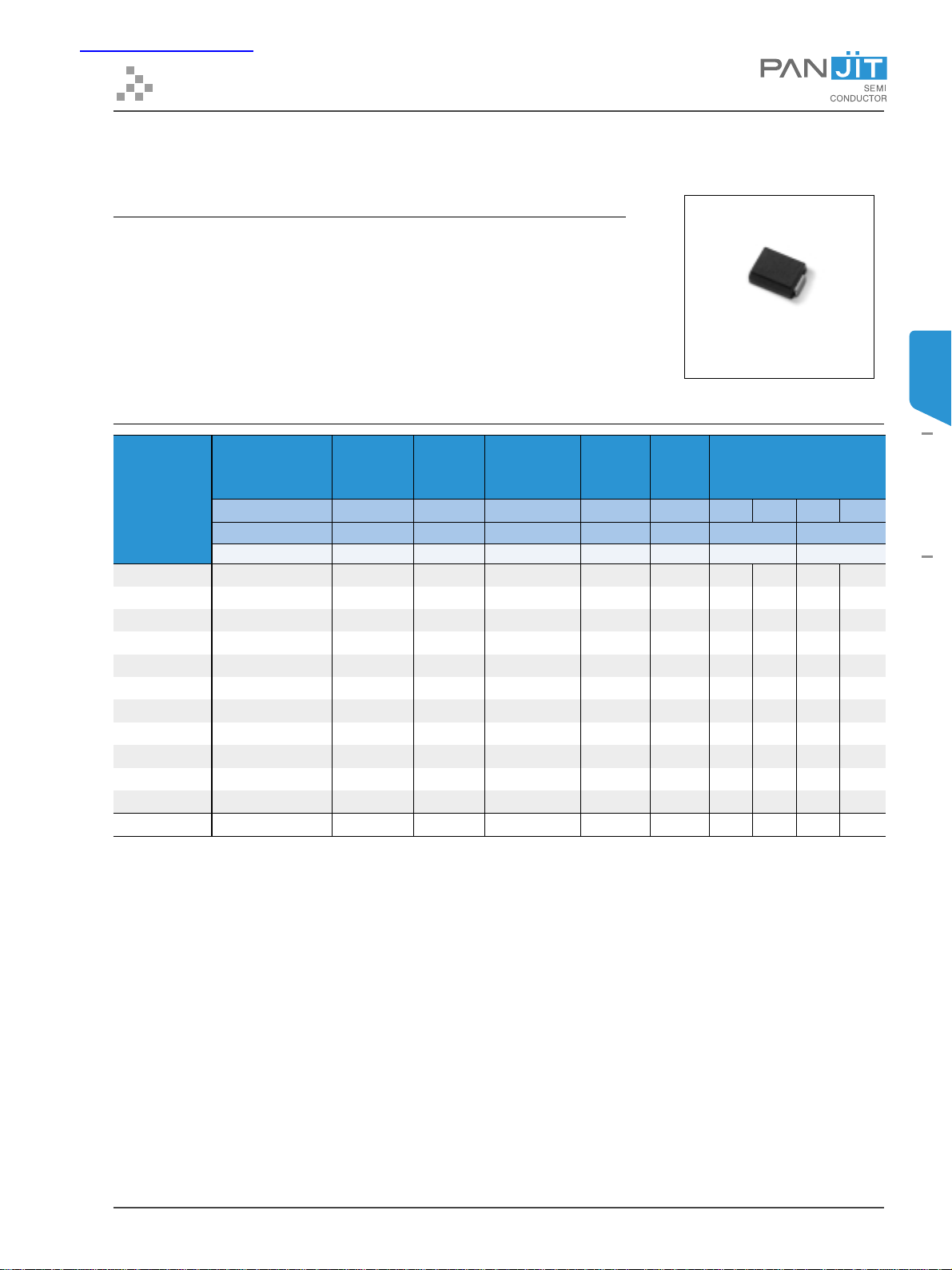
SMB/DO-214AA
gnidloH
tenrruC
cd
CO V05@
ecnaticapaCetatS-ffO
Vm51=caV,zHM1=f( RMS)
THYRISTOR
cd
TSP058SB - TSP320SB
NOTES:
1. Specific V
2. Specific IH values are available by request.
3. All ratings and characteristics are at 25 °C unless otherwise specified.
4. V
applies for the life of the device. I
DRM
5. V
is at 100V/msec, ISC =10Apk, VOC=1KVpk, 10/1000 Waveform
BO1
6. V
is at f = 60 Hz, ISC = 1 A
BO2
Ver: June 2001
values are available by request.
DRM
, Vac = 1KV
(RMS)
will be in spec during and following operation of the device.
DRM
, RL = 1 KΩ, 1/2 AC cycle
(RMS)
PAGE 1
PRELIMINARY
TSP058SB - TSP320SB
SELECTION GUIDE
Follow these steps to select the proper Thyristor surge protector for your application:
1. Define the operating parameters for the circuit:
• Ambient operating temperature range
• Maximum telephone line operating current (highest battery and shortest copper loop)
• Maximum operating voltage: (Maximum DC bias + peak ringing voltage)
• Maximum surge current
• System voltage damage threshold
• Select device with an off-state voltage rating (V
3. Select surge current ratings (I
4. Verify that the minimum holding current of the device at the maximum ambient temperature is above the maximum dc current of the
system.
5. Verify that the maximum breakover voltage of the device is below the system damage threshold.
6. Verify that the circuit's ambient operating temperatures are within the device's operating temperature range.
7. Verify that the device's dimensions fit the application's space considerations.
8. Independently evaluate and test the suitability and performance of the device in the application
PPS
and I
) ≥ those which the application must withstand.
TSM
) above the maximum operating voltage at the minimum operating temperature.
DRM
THYRISTOR
MAXIMUM SURGE RATINGS (TJ = 25 ºC UNLESS OTHERWISE NOTED)
gnitaR tnerruCesluPkaePevititepeR-noN
lobmyS I
evaWtnerruCtiucriC-trohS01/2 µs02/8 µs061/01 µs013/5 µs065/01 µs0001/01 µs
evaWegatloVtiucriC-nepO 01/2 µs 05/2.1 µs 061/01 µs 007/01 µs 065/01 µs 0001/01 µs
eulaV
setoN )6,5,4,2,1( )4,3,2,1(
Notes:
1. Thermal accumulation between successive surge tests is
not allowed.
2. The device under test initially must be in thermal
equilibrium with TJ = 25 °C.
3. Test at 1 cycle, 60 Hz.
4. Surge ratings are non-repetitive because instantaneous
junction temperatures may exceed the maximum rated TJ.
Nevertheless, devices will survive many surge applications
without degradation. Surge capability will not degrade over
a device's typical operating life.
5. Adjust the surge generator for optimum current-wave
accuracy when both voltage and current wave
specifications cannot be exactly met. The current wave is
more important than the voltage wave for accurate surge
evaluation.
6. The waveform is defined as A/B ms where:
A: (Virtual front time) = 1.25 X Rise time = 1.25 X (Tb - Ta)
B (Duration time to 50% level of Ipps) = T1 - T
A003A522A051A511A001A08
0
PPS
% Ipps
100%
80%
60%
40%
20%
0%
TbTa T1To
Time
I
TSP058SB - TSP320SB
kaePevititepeR-noN
tnerruCegruSetatS-nO
TSM
A03
Ver: June 2001
PAGE 2

PRELIMINARY
TSP058SB - TSP320SB
MAXIMUM THERMAL RATINGS
gnitaR lobmyS eulaV
Notes:
PCB board mounted on minimum foot print.
egnaRerutarepmeTnoitcnuJegarotS TSTG 051ot05-
egnaRerutarepmeTnoitcnuJgnitarepOT
egnaRerutarepmeTtneibmAgnitarepO Ta 56ot04-
J 051ot04-
tinU
O
C
O
C
O
C
THERMAL CHARACTERISTICS
citsiretcarahC lobmyS eulaV tinU
TsdaeLotnoitcnuJecnatsiseRlamrehT
L
Notes:
The junction to lead thermal resistance represents a minimum limiting value with both leads soldered to a large near-infinite heatsink. The
junction to ambient thermal resistance depends strongly on board mounting conditions and typically is 3 to 6 times higher than the junction
to lead resistance. The data shown is to be used as guideline values for preliminary engineering.
ottnecajdabatno
.sezisdaplacitnediotderedlossdaelhtoB.citsalp
R
θ LJ
02.xaM
O
W/C
THYRISTOR
TSP058SB - TSP320SB
ELECTRICAL CHARACTERISTICS (TC = 25°C UNLESS OTHERWISE NOTED)
sretemaraP snoitidnoCtseT lobmyS .niM .xaM tinU
kaePevititepeR
1tnerruCgnidloH0001/01 µ I,mrofevaws
egatloVetatS-nO I
Notes:
Specific IH values are available by request.
tnerruCetatS-ffO
tnerruCrevokaerB I,zH06=f
D Vdetar=
V
T
DRM
SC
V,smrA1= ca R,smrVK1=
CS V,A01= CO R,V26=
003=wT,A1= µ eslup1,s VT 5 V
L
K1= Ω elcycCA2/1, I OB 008 Am
L
004= Ω IH 051Am
I
DRM
5
µA
Ver: June 2001
PAGE 3

PRELIMINARY
TSP058SB - TSP320SB
+I
IPPS
ITSM
IT
IBO
IH
IBR
_
V
VT
_
I
citsiretcarahC lobmyS eulaV
V
IDRM
BO
I
BO
H
I
egatloVrevokaerB
tnerruCrevokaerB V(egatlovrevokaerbehttagniwolftnerrucsuoenatnatsnI
tnerruCgnidloH etats-noehtniecivedehtniatniamotderiuqertnerrucmuminiM
VDRM
VBR
VBO
+V
THYRISTOR
TSP058SB - TSP320SB
esirfoetartnerrucdnaegatlovdeificepsarednu
derusaemnwodkaerbtaroniecivedehtssorcaegatlovmumixaM
BO
)
I
T
V
V
DRM
I
DRM
I
PPS
Ver: June 2001
T
td/idtnerrucetats-nofoesirfoetarlacitirC
td/vd egatloVetatS-ffOfoesiRfoetaRlacitirC
tnerrucetats-nO noitidnocetats-noehtniecivedehthguorhttnerruC
egatlovetats-nO
egatloVetatS-ffOkaePevititepeRdetaR
tnerruCetatS-ffOkaePevititepeR
tnerruceslupkaePevititepeR-noN
Vfo
DRM
T
)
(tnerrucI
segatlov
tsetrednu
deificepsatanoitidnocetats-noehtniecivedehtssorcaegatloV
llagnidulcni,egatlovetats-ffoehtfoeulavsuoenatnatsnitsehgihehT
tneisnartevititepernonllagnidulcxetubsegatlovtneisnartevititeper
noitacilppaehtmorfstlusertahttnerrucfoeulav)kaep(mumixamehT
edutilpmadeificepsfotnerruceslupmikaepfoeulavmumixamdetaR
ecivedehtotegamadtuohtiwdeilppaebyamtahtepahsevawdna
.egamadtuohtiw
Vwoleb(egatlovfoesirfoetarmumixamehT
DRM
.etats-noehtotetats-ffoehtmorfgnihctiws
dnatshtiwnacecivedehttahttnerrucfoesirfoetarehtfoeulavdetaR
esuactonlliwtaht)
PAGE 4

PRELIMINARY
TSP058SB - TSP320SB
CAPACITANCE CHARACTERISTICS
F = 1 MHz, Vac = 15 mV
rms
rebmuNtraP
BS850PST 07 001 95 47 35 86 54 95 42 92
BS560PST76098596253634652282
BS570PST 76 87 65 46 94 85 24 94 32 72
BS090PST75168405246453839112
BS021PST 05 85 24 54 83 05 13 33 71 02
BS041PST94450434633403236191
BS061PST 64 35 83 04 43 63 82 03 51 81
BS091PST54358393335382034181
BS022PST 44 25 73 93 23 53 72 03 31 81
BS572PST44157393234372923181
BS023PST 34 05 73 83 23 43 72 92 31 71
MECHANICAL DATA
C
O
Fp
cdV0 cdV1 cdV2 cdV5 cdV05
.pyT .xaM .pyT .xaM .pyT .xaM .pyT .xaM .pyT .xaM
ecnaticapaCetatS-ffO
THYRISTOR
TSP058SB - TSP320SB
• Case: JEDEC DO-214AA molded plastic
• Terminals: Solder plated, solderable per MIL-STD-750,
Method 2026
• Polarity: Bi-directional Standard packaging: 12mm tape
(EIA-481)
• Weight: 0.003 ounce, 0.093 gram
SMB / DO-214AA
.083 (2.11)
.075 (1.91)
.096 (2.44)
.083 (2.13)
.050 (1.27)
.030 (0.76)
.185 (4.70)
.160 (4.06)
.220 (5.59)
.200 (5.08)
.008(.203)
.002(.051)
Unit: inch ( mm )
.155 (3.94)
.130 (3.30)
.012 (.305)
.006 (.152)
Ver: June 2001
PAGE 5

PRELIMINARY
TSP058SB - TSP320SB
DEVICE MARKING CODE
rebmuNtraP edoCgnikraM
BS850PST B850
BS560PSTB560
BS570PST B570
BS090PSTB090
BS021PST B021
BS041PSTB041
BS061PST B061
BS091PSTB091
BS022PST B022
BS572PSTB572
BS023PST B023
ORDER & PACKING INFORMATION
eciveD gnikcaP yt'QredrO.niM sAredrO krameR
leeR&epaT"31scp000,3BSxxxPSTgnikcaPdradnatS
BSxxxPST
leeR&epaT"7 scp005 7-BSxxxPST
PJ YM
058C
1st Line:
PJ-
YM-
2nd line:
PanJit logo
Last digit of calendar year
Month
Marking code
THYRISTOR
TSP058SB - TSP320SB
Ver: June 2001
PAGE 6

PRELIMINARY
TSP058SB - TSP320SB
RATING AND CHARACTERISTIC CURVES
90
80
Cseriesdevice
70
60
50
Capacitance (pF)
40
30
20
50 100 150 200 250 300 350
f=1 MHZ
Bseriesdevice
V =0VoltsDC
D
Aseriesdevice
V (V)
DRM
v =15mV AC
dRMS
O
T=25 C
J
TYPICAL CAPACITANCE V.S. RATED REPETITIVE OFF-STATE VOLTAGE
100
10
TSP220SC
m
1
Capacitance (pF)
70
60
50
40
30
20
10
0.1
f=1 MHZ
TSP075SC
TSP120SC
1
V Off-state Voltage (V)
D
v =15mV AC
dRMS
10 100
T=25 C
J
TSP140SC
TSP190SC
O
TYPICAL CAPACITANCE V.S. OFF-STATE VOLTAGE
THYRISTOR
TSP058SB - TSP320SB
0.1
0.01
D,
I Off-State Current ( A)
0.001
0.0001
0 20 40 60 80 100 120 140
TSP220SB
T(C)
TSP220SB
150
O
J
TYPICAL OFF-STATE CURRENT V.S JUNCTION TEMPERATURE
IMPORTANT NOTICE
This information is intended to unambiguously characterize the product in order to facilitate the customer's evaluation of the device in the
application. It will help the customer's technical experts determine that the device is compatible and interchangeable with similar devices
made by other vendors. The information in this data sheet is believed to be reliable and accurate. The specifications and information
herein are subject to change without notice. New products and improvements in products and their characterization are constantly in
process. This provides a superior performing and the highest value product. The factory should be consulted for the most recent informa-
tion and for any special characteristics not described or specified.
© Copyright PanjIt International Inc. 2001
All rights are reserved. Reproduction in whole or in part is prohibited without the prior written consent of the copyright owner.
The information presented in this document does not form part of any quotation or contract, is believed to be accurate and reliable and may changed without notice. No liability will be
accepted by the publisher for any consequence of its use.
Publication thereof does not convey nor imply any license under patent- or other industrial or intellectual property rights.
PanJit Internatioal Inc.
http://www.panjit.com.tw email: sales@panjit.com.tw
Ver: June 2001
PAGE 7
 Loading...