Panjit BAL99, BAV70, BAV99, BAW56 Schematic [ru]

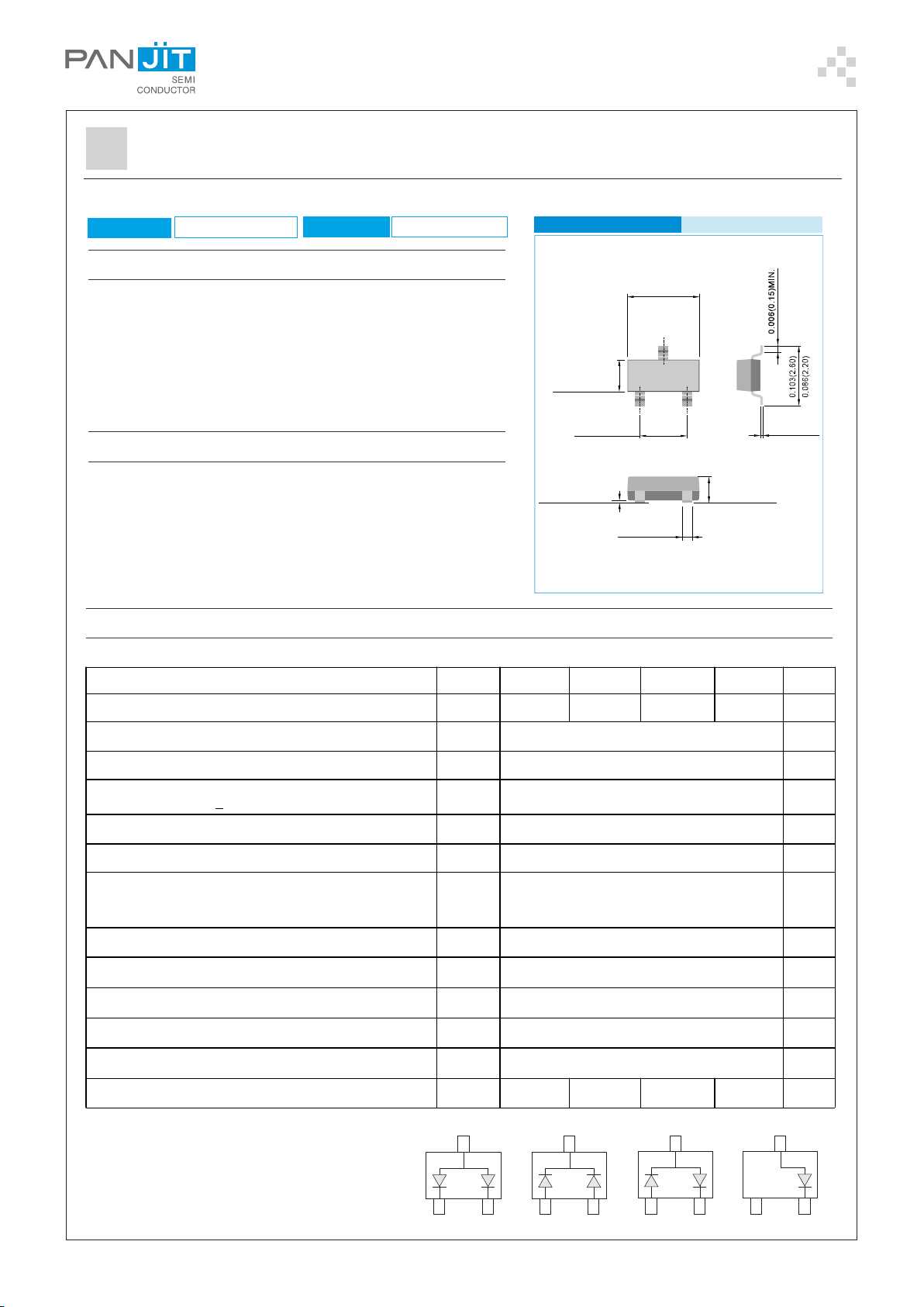
BAW56 / BAV70 / BAV99 / BAL99
Fig.15
COMMON ANODE
Fig.16
COMMON CATHODE
Fig.17
SERIES
Fig.18
SINGLE(Alt
)
SURFACE MOUNT SWITCHING DIODES
VOLTAGE
100 Volts
FEATURES
• Fast switching speed.
• Surface mount package Ideally Suited for Automatic insertion
• Electrically Identical to Standard JEDEC
• High Conductance
• Lead free in comply with EU RoHS 2002/95/EC directives.
• Green molding compound as per IEC61249 Std. . (Halogen Free)
POWER
250mWatts
SOT-23
0. 056 (1 .4 0)
0. 047 (1 .2 0)
Un it in ch( mm ):
0. 120 (3 .0 4)
0. 110( 2. 80 )
0. 008 (0 .2 0)
0. 003 (0 .0 8)
MECHANICAL DATA
0. 079 (2 .0 0)
0. 070 (1 .8 0)
• Case: SOT-23, Plastic
• Terminals: Solderable per MIL-STD-750, Method 2026
• Apporx. Weight: 0.0003 ounces, 0.0084 grams
0. 004 (0 .1 0)
0. 000 (0 .0 0)
0. 020 (0 .5 0)
0. 013 (0 .3 5)
0. 044 (1 .1 0)
0. 035 (0 .9 0)
MAXIMUM RATINGS AND ELECTRICAL CHARACTERISTICS
Ratings at 25OC ambient temperature unless otherwise specified. For capacitive load, derate current by 20%.
PARAMETER SYMBOL BAW56 BAV70 BAV99 BAL99 UNITS
Marking Code - JC JA JB JF -
Reverse Voltage V
Peak Reverse Voltage V
Rectified Current (Average), Half Wave Rectification with
Resistive Load and f >
50 Hz
Peak Forward Surge Current,0.001ms I
Power Dissipation Derate Above 25OC P
Maximum Forward Voltage V
Maximum DC Reverse Current at 25V
75V
Maximum Junction Capacitance (Notes 1) C
I
FSM
I
RM
TOT
R
R
O
F
0.855 @ I
1.25 @ I
J
75 V
100 V
150 mA
4.0 A
250 mW
0.715 @ I F=1mA
F
1.0 @ I
=10mA
F
=50mA
F
=150mA
0.03
2.5
1.5 pF
V
μA
September 30,2010-REV.00
Maximum Reverse Recovery Time (Notes 2) t
Typical Thermal Resistance
Junction Temperature Range T
Circuit Fi gure -
NOTE:
1. CJ at VR=0, f=1MHz
2.From IF=10mA to IR=1mA, VR=6Volts, RL=100Ω
rr
R
θ
JA
R
θ
JC
J
Common
Anode
COMMON CATHODE
Common
Cathode
4.0 ns
360
205
-55 to +150
Series Si ngle(Alt) -
O
C / W
O
C
PAGE . 1

BAW56 / BAV70 / BAV99 / BAL99
September 30,2010-REV.00
PAGE . 2
 Loading...