

Page 1
TO:
作成日 Issue Date:
改订日 Revision Date:
规格书编号
File No.
PN-RD-0023B
2012 年(Y)09 月(M)25 日(D)
2012 年(Y)11 月(M)02 日(D)
《新规 · 变更》
New Revision
产 品 规 格 书
Product Specification
【接收印栏】
产品名
Product
机种名
Model
TFT-LCD OPEN CELL
LC315TU3A
※ 本基准书由封面、附件等全 23 页构成。
如果对该规格书有异议,请在下订单前提出。
※ This Product Specification have 23 pages including the coversheet and Appendices. Please negotiate
the objection point before purchase order.
中电熊猫集团
南京中电熊猫液晶显示科技有限公司
研发中心 设计整合部
CEC PANDA GROUP
NANJING CEC PANDA LCD TECHNOLOGY CO., LTD.
R&D CENTER, DESIGN INTEGRATION SECTION.
Page 2

PANDA
LC315TU3A Specification Version 1.0
-CONTENTS –
RECORDS OF REVISION .............................................................................................................. 3
1. APPLICATION ............................................................................................................................... 4
OVERVIEW ................................................................................................................................... 4
2.
3. MECHANICAL TECHNICAL LITERATURES ............................................................................... 4
4. PIXEL ARRAY AND MEMBER LOCATION .................................................................................. 5
5. INPUT TERMINALS ...................................................................................................................... 5
5.1 TFT PANEL DRIVING............................................................................................................................... ..............5
5.2 INTERFACE BLOCK DIAGRAM.......................................................................................................................... 7
5.3 BLOCK DIAGRAM (OPEN-CELL)....................................................................................................................... 7
6. ELECTRICAL CHARACTERISTICS ............................................................................................. 9
6.1 ABSOLUTE MAXIMUM RATING.......................................................................................................................... 9
6.2 CONTROL CIRCUIT DRIVING..............................................................................................................................9
7. TIMING CHARACTERISTICS OF INPUT SIGNALS .................................................................. 11
7.1 TIMING CHARACTERISTICS.............................................................................................................................11
7.2 LVDS SIGNAL CHARACTERISTICS................................................................................................................. 12
8. INPUT SIGNAL, BASIC DISPLAY COLORS AND GRAY SCALE OF EACH COLOR .............. 14
OPTICAL CHARACTERISTICS .................................................................................................. 15
9.
10. HANDLING PRECAUTIONS OF THE OPEN-CE LL ................................................................... 17
11. PACKING FORM ......................................................................................................................... 17
12. RELIABILITY TEST ITEM ........................................................................................................... 18
13. OTHERS ...................................................................................................................................... 19
14. EPS BOX STORAGE CONDITION ............................................................................................. 20
15. PRECAUTIONS ........................................................................................................................... 20
2
Page 3

PANDA
r
LC315TU3A Specification Version 1.0
RECORDS OF REVISION
DATE NO.
REVISED
MODEL No. : LC315TU3A
PAGE SUMMARY NOTE
No.
2012/09/25 PN-RD-0023B T1.0 23 First Edition
P5. Change the Using connecto
2012/11/02 PN-RD-0023B V1.0
5,6,9,
P6.Add BIST mode function.
P9.Update the date of I
15
P15.Update
optical characteristics.
CC, IRUSH.
type.
Tentative
Final
3
Page 4

PANDA
r
LC315TU3A Specification Version 1.0
1. APPLICATION
This technical literature applies to the color 31.5” Wide XGA TFT-LCD LC315TU3A.
* These specification sheets are proprietary products of Nanjing CEC-Panda LCD Technology Co., LTD
(“CPL”) and include materials protected under copyright of CPL. Do not reproduce or cause any third
party to reproduce them in any form or by any means, electronic or mechanical, for any purpose, in
whole or in part, without the express written permission of CPL.
* This module is not designed to use in dusty environment and to prevent image retention caused by
long-term display of fixed pattern. So please consider items mentioned above before use and design
equipment.
* In case of using the device for applications such as control and safety equipment for transportation
(aircraft, trains, automobiles, etc.), rescue and security equipment and various safety related equipment
which require higher reliability and safety, take into consideration that appropriate measures such as
fail-safe functions and redundant system design should be taken.
* Do not use the device for equipment that requires an extreme level of reliability, such as aerospace
applications, telecommunication equipment (trunk lines), nuclear power control equipment and medical
or other equipment for life support.
* CPL assumes no responsibility for any damage resulting from the use of the device that does not
comply with the instructions and the precautions specified in these technical literature.
* Contact and consult with a CPL sales representative for any questions about this device.
2. OVERVIEW
This module is color active matrix LCD Open-cell incorporating amorphous silicon TFT (Thin Film
Transistor). It is composed of a color TFT-LCD panel, driver ICs, etc. Graphics and texts can be
displayed on a 1366×RGB×768 dots panel with about 16,777,216 colors(R/G/B 8bit in each color) by
using LVDS(Low Voltage Differential Signaling) to interface, +12V of DC supply voltage.
In order to improve the response time of LCD, this module applies the Over Shoot driving (O/S
driving) technology for the control circuit. In the O/S driving technology, signals are being applied to the
Liquid Crystal according to a pre-fixed process as an image signal of the present frame when a
difference is found between image signal of the previous frame and that of the current frame after
comparing them.
By using the captioned process, the image signals of this LCD module are being set so that image
response can be completed within one frame, as a result, image blur can be improved and clear image
performance can be realized.
3. MECHANICAL TECHNICAL LITERATURES
Paramete
Display size
Active area 697.685(H) x 392.256(V) mm
Pixel Format
Pixel pitch 0.51075(H) x 0.51075 (V) mm
Pixel configuration R, G, B vertical stripe
Display mode Normally black
Outline Dimensions (*1),(*2)
Mass 1.18±0.1 kg
Surface treatment(*2)
Hard coating: 3H(CF Side)/ None(TFT Side )
(*1) Outline dimensions are shown in Fig.3-1, 3-2.
(*2) This specification is without the protection film.
Technical literatures Unit
80.039 (Diagonal) cm
31.5 (Diagonal) inch
1366(H) x 768(V)
(1pixel = R+G+B)
715.7(H) x455.5(V) x 4.0 (D)
(Open cell (with PWB))
715.7(H)×411.2(V)×1.75(D)
( Multi-cell (Without PWB) )
Anti glare
Low haze (15 or less)
4
pixel
mm
mm
Page 5
PANDA
LC315TU3A Specification Version 1.0
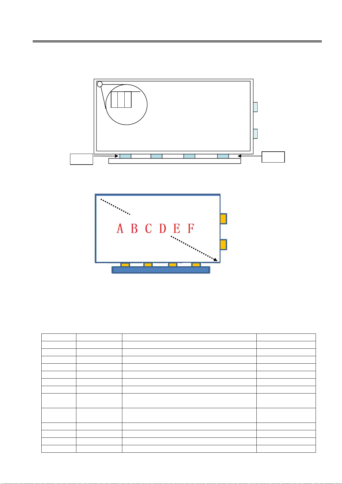
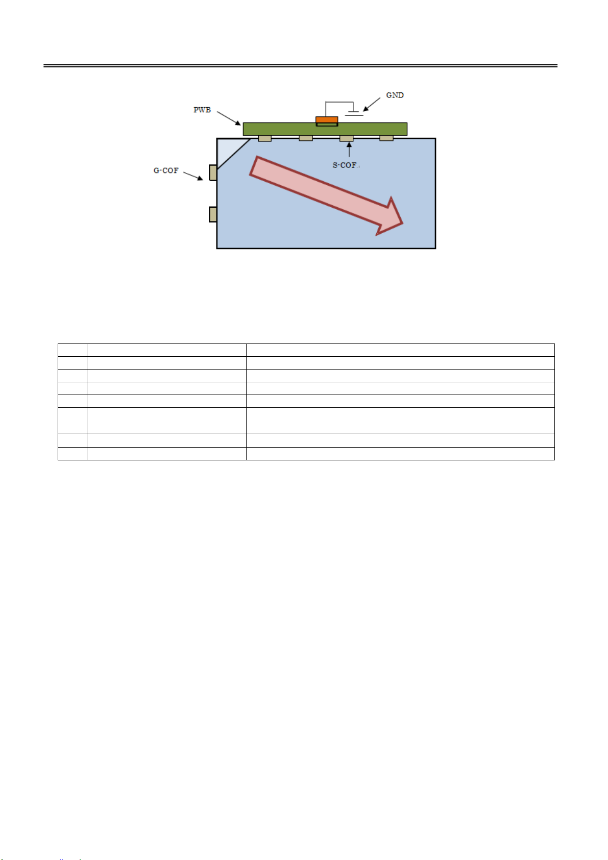
4. PIXEL ARRAY AND MEMBER LOCATION
Pixel array and member located as below.
There are 4 Source Drivers (1026 input terminals S-Dr) on this panel.
R
B
G
(1,1)
(1366,768)
COF 4
Please use this Open Cell like following figure.
Fig.4-1 Pixel array and member location
Scan direction
Fig.4-2 Scan direction
5. INPUT TERMINALS
5.1 TFT PANEL DRIVING
CN1 (Interface signals and +12V DC power supply) shown on the next table.
Using connector:
Matching connector: FI-X30C2L(Japan Aviation Electronics Ind., Ltd) or equivalent device.
Matching LVDS transmitter: THC63LVDM83R (THine) or equivalent device.
Pin No. Symbol Remark
1 VCC +12V Power Supply
2 VCC +12V Power Supply
3 VCC +12V Power Supply
4 VCC +12V Power Supply
5 GND Ground
6 GND Ground
7 GND Ground
8 WP
9 SELLVDS Select LVDS data format[Note1] Default: pull down
10 Reserved Not Available
11 GND Ground
12 RIN0- Negative(-) LVDS differential data input LVDS
13 RIN0+ Positive(+) LVDS differential data input LVDS
FI-X30SSLA-HF-R2500(Japan Aviation Electronics Ind.,Ltd) or equivalent device.
EEPROM Write Protection (for P-Vcom)
(0V~0.7V_Disable,2.7V~3.3V/Open _Enable)
5
COF 1
(L:GND) [Note2]
Page 6
PANDA
LC315TU3A Specification Version 1.0
14 GND Ground
15 RIN1- Negative(-) LVDS differential data input LVDS
16 RIN1+ Positive(+) LVDS differential data input LVDS
17 GND Ground
18 RIN2- Negative(-) LVDS differential data input LVDS
19 RIN2+ Positive(+) LVDS differential data input LVDS
20 GND Ground
21 CLKIN- Clock Signal(-) LVDS
22 CLKIN+ Clock Signal(+) LVDS
23 GND Ground
24 RIN3- Negative(-) LVDS differential data input LVDS
25 RIN3+ Positive(+) LVDS differential data input LVDS
26 GND Ground
27 NC Not connection, this pin should be open. [Note 3]
28 SCL Serial clock input (for P-Vcom)
29 SDA Serial data input (for P-Vcom)
30 GND Ground
[Note 1] SELLVDS
Transmitter SELLVDS
Pin No Data
51 TA0 R0(LSB) R2
52 TA1 R1 R3
54 TA2 R2 R4
55 TA3 R3 R5
56 TA4 R4 R6
3 TA5 R5 R7(MSB)
4 TA6 G0(LSB) G2
6 TB0 G1 G3
7 TB1 G2 G4
11 TB2 G3 G5
12 TB3 G4 G6
14 TB4 G5 G7(MSB)
15 TB5 B0(LSB) B2
19 TB6 B1 B3
20 TC0 B2 B4
22 TC1 B3 B5
23 TC2 B4 B6
24 TC3 B5 B7(MSB)
27 TC4 NA NA
28 TC5 NA NA
30 TC6 DE(*) DE(*)
50 TD0 R6 R0(LSB)
2 TD1 R7(MSB) R1
8 TD2 G6 G0(LSB)
10 TD3 G7(MSB) G1
16 TD4 B6 B0(LSB)
18 TD5 B7(MSB) B1
25 TD6 NA NA
NA: Not Available
(*)The display position is prescribed by the rise of DE (Display Enable) signal, please do not fix DE
signal during operation at "High."
VESA
= L(GND) or Open
6
JEITA
=H(3.3V)
Page 7

PANDA
(15)
(
)
LC315TU3A Specification Version 1.0
[Note 2] The equivalent circuit figure of the terminal
Fig.5-1 The equivalent circuit figure of the terminal
[Note 3] Built-in Self Test (BIST)
*1) PIN27=NC: Disable BIST function.
Available LVDS Signal input : Display LVDS input Pattern.
No LVDS Signal or unavailable LVDS Signal input : Display Black Pattern.
*2) PIN27=High (3.0V~3.6V) : Enable BIST function.
Available LVDS Signal input : Display LVDS input Pattern.
No LVDS Signal or unavailable LVDS Signal input : Display BIST Pattern.
5.2 INTERFACE BLOCK DIAGRAM
Corresponding Transmitter: THC63LVDM83R (THine) or equivalent device.
(TVside)
R0~R7
G0~G7
B0~B7
ENAB
(controller)
8
8
8
CLK
LVDS
TTL
PLL
Rx1IN0+(13)
Rx1IN0-(12)
Rx1IN1+(16)
Rx1IN1Rx1IN2+(19)
Rx1IN2-(18)
Rx1IN3+(25)
Rx1IN3-(24)
Rx1CLKIN+(22)
Rx1CLKIN-(2 1)
TFT - LCD side
8
R0~R7
LVDS
TTL
PLL CLK
8
8
G0~G7
B0~B7
ENAB
Internal circuits
Fig.5-2 Interface block diagram
5.3 BLOCK DIAGRAM (OPEN-CELL)
Fig.5-3 block diagram (Open-cell)
7
Page 8

PANDA
LC315TU3A Specification Version 1.0
R0~R7:Pixel R DATA(R7:MSB , R0:LSB)
G0~G7:Pixel G DATA(G7:MSB , G0:LSB)
B0~B7:Pixel B DATA(B7:MSB , B0:LSB)
DE:DATA enable Signal
Fig.5-4 LVDS data map
8
Page 9

PANDA
r
LC315TU3A Specification Version 1.0
6. ELECTRICAL CHARACTERISTICS
6.1 ABSOLUTE MAXIMUM RATING
Paramete
Input voltage VI
+12V supply voltage VCC
Storage temperature T
Operation temperature T
[Note 1] SELLVDS
[Note 2] Max Humidity: 90%RH. (Ta≦40℃)
6.2 CONTROL CIRCUIT DRIVING
+12V supply
voltage
Permissible input ripple
Differential input
threshold
voltage
Input Low voltage VIL 0 0.7 V
Input High voltage
Symbol Condition Ratings Unit Remark
-
stg
-
opa
Wet-bulb temperature should be 39℃Max. (Ta>40℃).
No condensation.
Parameter Symbol Min. Typ. Max. Unit Remark
Supply voltage
Current
dissipation
voltage
High
Low
V
ICC
IRUSH
V
VTH
V
V
Ta= 25℃ -0.3~3.6
Ta= 25℃ 0~+14
-20~+60
0~+50
CC
RP
TL - - -100 mV
IH
+10.8 +12.0 +13.2 V [Note 1]
- 350 600 mA [Note 2]
- - 6 A [Note 5]
- - 100 mVp-p Vcc=+12.0V
100 - - mV
2.7 - 3.3 V
V [Note 1]
V
℃
℃
[Note 2]
[Note 4]
[Note 3]
Input leak current (Low) IIL - - 400 µA VI=0V [Note 3]
Input leak current (High) IIH - - 100 µA VI =3.3V [Note 3]
Terminal resistor RT - 100 - Ω Differential input
Input Differential voltage |VID| 200 400 600 mV [Note 4]
Differential input
common mode voltage
VCM: Common mode voltage of LVDS driver.
[Note 1]
Input voltage sequences
50us ≦ t1 ≦ 20ms a) 9.1V ≦ V
20ms < t2-1 td ≦ 10ms
20ms < t2-2 b) V
0 < t3-1≦1s Dip conditions for supply voltage is
0 < t3-2≦1s based on input voltage sequence.
1s ≦ t4
500ms ≦ t5-1
500ms ≦ t5-2
0 < t6-1
0 < t6-2
VCM |VID|/2 1.2
2.4-|VID|/2
Dip conditions for supply voltage
< 9.1V
CC
V [Note 4]
< 10.8V
CC
9
Page 10

PANDA
LC315TU3A Specification Version 1.0
0.1Vcc
V cc
Data1
Data2
B a ck lig h t:V
0.9Vcc
t1
t2-1
t2-2
INV
t5-1
OFF
t5-2
ON
ON
ON
t6-2
t6-1
t3-1
t3-2
0.9Vcc
0.1Vcc 0.1Vcc
t4
td
OFF
Fig. 6-1 Input voltage sequences Fig. 6-2 Dip conditions for supply voltage
Vcc
10.8V
9.1V
* Data1: CLKIN±,RIN0±,RIN1±, RIN2±, RIN3±
* Data2: SELLVDS
* About the relation between data input and back light lighting, please base on the above-mentioned
input sequence.
When back light is switched on before panel operation or after a panel operation stop, it may not
display normally. But this phenomenon is not based on change of an incoming signal, and does not
give damage to a liquid crystal display.
[Note 2] Typical current situation: 256 gray-bar pattern (VCC = +12.0V).
The explanation of RGB gray scale is seen in section 8.
Fig. 6-3 Typical current situation
[Note 3] SELLVDS
[Note 4] CLKIN+/CLKIN-, RIN0+/RIN0-, RIN1+/RIN1-, RIN2+/RIN2-, RIN3+/RIN3-
*CK-, *IN-
*CK+, *IN+
GND
Fig. 6-4 LVDS input characteristics
V
TH
VTL
|VID|
VCM
10
Page 11

PANDA
0.1 Vcc
500us
LC315TU3A Specification Version 1.0
[Note 5] The Rush current corrugation at the time of power on.
Ton: Vcc(+12V) Rising Time
0.9 Vcc
Vcc=12V
I
RUSH
Current of Vcc 12V
Fig. 6-5 The waveform of rush current
7. TIMING CHARACTERISTICS OF INPUT SIGNALS
7.1 TIMING CHARACTERISTICS
Parameter Symbol Min
Frequency Fclk=1/Tc 72 82 82 85 MHz
Spread Spectrum
Clock
Data
enable
signal
*Timing diagrams of input signal are shown in Fig. 7-1.
* SSCG (Spread spectrum clock generator) is defined as Fig. 7-2.
Modulation range
Spread Spectrum
Modulation frequency
Horizontal period TH
Horizontal period
(High)
Horizontal Blanking
period
Vertical period TV
Vertical period (High) TVd 768 768 768 768 line
Vertical Blanking
period
Fclk_mod Fclk-3%
SSM
F
THd 1366 1366 1366 1366 clock
TH-THd 174 330 330 574 clock
TV-TVd 10 38 199 204 line
30
1540 1696 1696 1940 clock
17.15 20.68 20.68 21.42 µs
778 806 967 972 line
47.7 60 50 62.35 Hz
From 10%Vcc to 90%Vcc
I: Current of Vcc(+12V)
I
RUSH
After Vcc rise.
[HOW TO]
Measure the Vcc(12V) when you turn
the power on. At the same time,
measure the current of Vcc(12V).
The single mode of the oscilloscope is
useful in this case.
NTSC PAL
--
--
: The max current
Typ.
Max. Unit
Fclk+3% MHz
100 KHz
11
Page 12

PANDA
LC315TU3A Specification Version 1.0
Fig.7-1 Timing characteristics of input signals
Fig.7-2 Spread spectrum clock generator
7.2 LVDS SIGNAL CHARACTERISTICS
CLKCLK+
RINxRINx+
tpd0
Vdiff=0V
tpd1
tpd2
tpd3
tpd4
tpd5
tpd6
Fig.7-3 LVDS signal characteristics
t
CLK
12
Page 13

PANDA
Delay time, CLK rising edge
to serial bit position 0
Delay time, CLK rising edge
to serial bit position 1
Delay time, CLK rising edge
to serial bit position 2
Data
position
Delay time, CLK rising edge
to serial bit position 3
Delay time, CLK rising edge
to serial bit position 4
Delay time, CLK rising edge
to serial bit position 5
Delay time, CLK rising edge
to serial bit position 6
LC315TU3A Specification Version 1.0
The item Symbol min. typ. Max. unit
tpd0
tpd1
tpd2
tpd3
tpd4
tpd5
tpd6
-0.40 0 0.40
typ-0.40
typ-0.40
typ-0.40
typ-0.40
typ-0.40
typ-0.40
1*
2*
3*
4*
5*
6*
t
/7
CLK
t
/7
CLK
t
/7
CLK
t
/7
CLK
t
/7
CLK
t
/7
CLK
typ+0.40
typ+0.40
typ+0.40
typ+0.40
typ+0.40
typ+0.40
ns
13
Page 14

PANDA
LC315TU3A Specification Version 1.0
8. INPUT SIGNAL, BASIC DISPLAY COLORS AND GRAY SCALE OF EACH COLOR
0: Low level voltage,
1: High level voltage.
Each basic color can be displayed in 256 gray scales from 8 bit data signals. According to the
combination of total 24 bit data signals, the 16,777,216 colors display can be achieved on the screen.
Fig.8-1 Input Signal
14
Page 15

PANDA
LC315TU3A Specification Version 1.0
9. OPTICAL CHARACTERISTICS
Parameter Symbol Condition Min. Typ. Max. Unit Remark
Viewing
angle range
Contrast ratio CR
Horizontal
Vertical
θ21
θ22
θ11
θ12
CR≥10
Ta= 25 °C
- 88 - Deg.
[Note1,4]
- 88 - Deg.
- 5000 - - [Note2,4]
Response time
Chromaticity of white
Chromaticity of red
Chromaticity of green
Chromaticity of blue
White variation δW - - -
*The measurement shall be executed 60 minutes after lighting at rating.
*These values are measured with CPL LED back light unit.
*The optical characteristics are measured using the following equipment.
Detector(EZ-CONTRAST/ Photodiode)
τ
DRV
x
y 0.290 -
θ
x 0.637 y 0.350 x 0.294 y 0.638 x 0.149 y 0.074 -
=0 deg.
- 7 - ms [Note3,4,5]
0.272
Typ-0.03
500mm
-
Typ+0.03
1.3
Detector(SR-3)
- [Note 6]
[Note 4]
Middle of the screen (
TFT-LCD Module
Fig.9-1 Measurement of Viewing angle range
and Response time.
(Viewing angle range: EZ-CONTRAST,
Response time: Photodiode)
θ
=0°)
Field=2°
Middle of the screen (
TFT-LCD Module
Fig.9-2 Measurement of Contrast, Luminance,
Chromaticity, White variation
θ
=0°)
15
Page 16

PANDA
r
r
r
θ
θ11θ
θ
τ
LC315TU3A Specification Version 1.0
[Note 1] Definitions of viewing angle range:
Normal line
21
12
22
6 o’clock direction
Fig.9-3 Viewing angle
[Note 2] Definition of contrast ratio:
The contrast ratio is defined as the following.
Contrast Ratio =
Luminance (Brightness) with white screen
Luminance (Brightness) with black screen
[Note 3] Definition of response time
The response time (τ
) is defined as the following figure and shall be measured by switching
DRV
the input signal for “any level of gray (0%, 25%, 50%, 75% and 100%) and “any level of gray (0%,
25%, 50%, 75% and 100%).
0% 25% 50% 75% 100%
0%
25%
50%
75%
100%
:25%–0%
τ
d
:50%–0% τd:50%–25%
τ
d
:75%–0% τd:75%–25% τd:75%–50%
τ
d
:100%–0% τd:100%–25% τd:100%–50% τd:100%–75%
τ
d
τ
:0%–25% τr:0%–50% τr:0%–75% τr:0%–100%
τ
:25%–50% τr:25%–75% τr:25%–100%
r
τ
:50%–75% τr:50%–100%
τ
τ*:x-y...response time from level of gray(x) to level of gray(y)
=Σ (τ*:x-y)/20
τ
DRV
Photodetector
Output
(Relative Value)
any level of gray
(bright)
100%
90%
10%
0%
τd:*
any level of gray
(dark)
Fig.9-4 Response time
any level of gray
(bright)
:*
time
[Note 4] This shall be measured at center of the screen.
When black brightness is a max value, the specification of the contrast is satisfied.
[Note 5] This value is valid when O/S driving is used at typical input time value.
[Note 6] Definition of white variation:
White variation is defined as the following with five measurements. (A~E)
:75%–100%
16
Page 17

PANDA
LC315TU3A Specification Version 1.0
Fig.9-5 measurement locations of white variation
10. HANDLING PRECAUTIONS OF THE OPEN-CELL
a) Be sure to turn off the power supply when inserting or disconnecting the cable.
b) Be sure to design the cabinet so that the module can be installed without any extra stress such as
warp or twist.
c) Since the front polarizer is easily damaged, pay attention not to scratch it.
d) Since long contact with water may cause discoloration or spots, wipe off water drop immediately.
e) When the panel surface is soiled, wipe it with absorbent cotton or other soft cloth.
f) Since the panel is made of glass, it may break or crack if dropped or bumped on hard surface.
Handle with care.
g) Since CMOS LSI is used in this module, take care of static electricity and take the human earth
into consideration when handling.
h) The module has a printed circuit boards (PCB) on the back side, take care to keep it from any
stress or pressure when handling or installing the module; otherwise some of electronic parts on
the PCB may be damaged.
i) Observe all other precautionary requirements in handling components.
j) When some pressure is added onto the module from rear side constantly, it causes display
non-uniformity issue, functional defect, etc. So, please avoid such design.
k) When giving a touch to the panel at power on supply, it may cause some kinds of degradation. In
that case, once turn off the power supply, and turn on after several seconds again, and that is
disappear.
l) When handling LCD modules and assembling them into cabinets, please be noted that long-term
storage in the environment of oxidization or deoxidization gas and the use of such materials as
reagent, solvent, adhesive, resin, etc. which generate these gasses, may cause corrosion and
discoloration of the LCD modules.
m) This LCD module is designed to prevent dust from entering into it. However, there would be a
possibility to have a bad effect on display performance in case of having dust inside of LCD
module. Therefore, please ensure to design your TV set to keep dust away around LCD module.
11. P A CKING FORM
(a)Piling number of Pallet : 14 cell boxes/1 pallet
(b)Packing quantity in one EPS BOX : 15 pcs
(c)EPS BOX size : 829(L)×557(W)×141(H) mm
(d)Pallet size : 1140(L)×855(W)×150(H) mm
(e)Pallet size after packing(with 14 boxes) : 1140(L)×855(W)×1117(H) mm
(f) Total mass of one pallet filled with full open-cell : MAX 330 kg
17
Page 18

PANDA
LC315TU3A Specification Version 1.0
Spacer 16pcs
EPS BOX Body
EPS BOX Cover
Panel 15pcs
Cover Sheet
Corner Protector
Stretching film
PP Band 4pcs
PP BAND Protector
PP BAND 2pcs
Pallet
<7 Tiers 2 Rows>
Cell BOX Label
12. RELIABILITY TEST ITEM
No
.
High temperature storage test
1
Low temperature storage test
2
High temperature and high humidity
3
operation test
High temperature operation test
4
Low temperature operation test
5
Thermal shock test
6
7 Package vibration test
8 Package drop test
ESD
9
[Result evaluation criteria]
Under the display quality test condition with normal operation state, there shall be no change, which
may affect practical display function.
Test item Condition
Ta= 60°C 240h
Ta= -2 0°C 240h
Ta= 50°C ; 80%RH 240h
(No condensation)
Ta= 50°C 240h
Ta= 0°C 240h
-20℃/30mins, 60℃/30mins, 100 cycles
Wave form:Random
Vibration level:1.0 Grms
Frequency:5-50 Hz
Duration:X,Y,Z each direction per 10mins
Height:15cm (2 edges, 1 surface)
At the following conditions, it is a thing without
incorrect operation and destruction.
Both under Contact and Non-contact conditions,
apply electric discharge ±300V to the input terminal.
condition:200pF 0Ω under non-operation.
Carton Label
Cover Sheet
18
Page 19

PANDA
13. OTHERS
a) Panel label
a-1) The label of Multi-cell which is stuck on the front side of the panel.
15mm
a-2) The label of Open-cell which is stuck on component side of the PWB.
10mm
b) Packing label
b-1) EPS BOX b-2) Pallet
60mm
c) Adjusting volume has been set optimally before shipment, so do not change any adjusted value.
If adjusted value is changed, the specification may not be satisfied.
LC315TU3A Specification Version 1.0
P A N D A
XXX-XXXXXXXX-XXXX
XXXXXXXXX
PANDA
QUANTITY: 15
20XXXXXXXXXXX
RoHS
(a) Quantity
(b) Model No.
(c) Box ID
(d) Date
DATE: 20XX/XX/XX
MADE IN CHINA
Model No.
80mm
(a)
70mm
XXXXXXXXX
Panel ID
Fig.13-1 Multi-cell label
42mm
XXX-XXXXXXXX-XXXX
Fig.13-2 Open-cell label
XXXXXXXXX
(c)
Fig.13-3 Packing label
(b)
(d)
YYYY/MM/DD
Panel ID
客户名称:
物料代
出货日期:
19
RoHS
XX
Barcode
210mm
南京中电熊猫液晶显示科技有限公司
订单
名 :
品 名:
码
:
数 量:
栈
板号 :
检验
結果
合格
不合格
(e) Customer name
(f) Order No.
(g) Name of products
(h) Pallet No.
31.5”Open cell
LC315TU3A
210Pcs
质检
員
检验
日期
(e)
(f)
(g)
(b)
(a)
(h)
(d)
297mm
Page 20

PANDA
LC315TU3A Specification Version 1.0
d) Disassembling the module can cause permanent damage and should be strictly avoided.
e) Please be careful since image retention may occur when a fixed pattern is displayed for a long time.
f) The chemical compound, which causes the destruction of ozone layer, is not being used.
g) When any question or issue occurs, it shall be solved by mutual discussion.
Regulation to utilize an ozone depletion chemical substance.
h)
Restricted substance : CFCs, halon, carbon, tertrachloide, and 1,1,1-trichloroethane
This product don't include the above matter.
Production process of this product and parts don't include above matter.
14. EPS BOX STORAG E CONDITION
Temperature: 0°C to 40°C
Humidity: 80%RH or less
Reference condition: 20°C to 35°C, 80%RH or less (summer)
5°C to 15°C, 80%RH or less (winter)
The total storage time (40°C, 80%RH): 240h or less
Sunlight: Be sure to shelter a product from the direct sunlight.
Atmosphere: Harmful gas, such as acid and alkali which bites electronic components and/or wires
must not be detected.
Be sure to put cartons on palette or base, don’t put it on floor, and store them with removing from wall.
Please take care of ventilation in storehouse and around cartons, and control changing temperature is
within limits of natural environment.
Storage life 1 year
15. PRECAUTIONS
a) Because the Open-Cell is too weak to destroy by static electricity, please don’t touch the terminal
with bare hands.
b) Front polarizer can easily be damaged. Pay attention on it.
c) Since long contact with drops of water may cause discoloration or spots, please wipe off them as
soon as possible.
d) When the panel surface is soiled, wipe it with absorbent cotton or other soft cloth.
e) The Panel will be broken or chipped when it is dropped or bumped against a hard substance.
f) Precautions of peeling off the Protection film:
- Be sure to peel off slowly (recommended more than 7 sec.) and constant speed.
- Peeling direction shown in the Fig. 15-1.
- Be sure to ground person with adequate methods such as the anti-static wrist band.
- Be sure to connect PWB to GND while peeling off the protection film.
- Ionized air should be blown to the surface while peeling off the protection film.
- The protection film must not touch drivers and PWB.
- After the protection film has been peeled off, some adhesive may be remained on the polarizer.
Please use isopropyl-alcohol to remove it.
20
Page 21
PANDA
LC315TU3A Specification Version 1.0
Fig.15-1 Direction of peeling off
g) Since the Open-cell consists of TFT and electronic circuits with CMOS-ICs, which are very weak to
electrostatic discharge, persons who are handling an Open-Cell should be grounded though
adequate methods such as an anti-static wrist band. Connector pins should not be touched directly
with bare hands.
Reference: Process control standard of CPL.
item Management standard value and performance standard
1 Anti-static mat(shelf) 1to50[Mega ohm]
2 Anti-static mat(floor, desk) 1to100[Mega ohm]
3 Ionizer Attenuate from ±1000V to ±100V within two seconds.
4 Anti-static wrist band 0.8 to 10 [Mega ohm]
5 Anti-static wrist band entry and
ground resistance
6 Temperature
7 Humidity 60 to 70 [%]
h) Since the Open-cell has a PWB, please take care to keep it off any stress or pressure when
handling or installing the Open-cell, otherwise some of electronic parts on it may be damaged.
i) Be sure to turn off the power supply when inserting or disconnecting the cable.
j) Be sure to design the module and cabinet so that the Open-cell van is installed without any extra
stress such as warp or twist.
k) When handling and assembling Open-Cell into module, please be noted that long-term storage in
the environment of oxidization or deoxidization gas and the use of materials such as reagent,
solvent, adhesive, resin, etc. which generate these gasses, may cause corrosion and discoloration
of the Open-Cell.
l) Applying too much force and stress to PWB and drivers may cause a malfunction electrically and
mechanically.
m) The Open-cell has high frequency circuits. Sufficient suppression to EMI should be done by system
manufactures.
n) Please be careful since image retention may occur when a fixed pattern is displayed for a long
time.
o) The chemical compound, which causes the destruction of ozone layer, is not being used.
p) This Open-Cell module is corresponded to RoHS.
q) When any question or issue occurs, it shall be solved by mutual discussion.
Below 1000[ohm]
22 to 26 [℃]
21
Page 22

PANDA
LC315TU3A Specification Version 1.0
Fig.3-1. Front outline drawing
22
Page 23

PANDA
LC315TU3A Specification Version 1.0
Fig.3-2. Back outline drawing
23
 Loading...