

Page 1

TO :
规格书编号
File No.
PN-RD-0015A
作成日 Issue Date:
改订日 Revision Date:
2012 年(Y)07 月(M)16 日(D)
2012 年(Y)07 月(M)24 日(D)
《新规 · 变更》
New Revision
产 品 规 格 书
Product Specification
产品名
Product
TFT-LCD OPEN CELL
机种名
Model
LC185TT2A
【接收印栏】
※ 本基准书由封面、附件等全 18 页构成。
如果对该规格书有异议,请在下订单前提出。
※ This Product Specification have 18 pages including the coversheet and Appendices. Please negotiate the
objection point before purchase order.
中电熊猫集团
南京中电熊猫液晶显示科技有限公司
研发中心 设计整合部
CEC PANDA GROUP
NANJING CEC PANDA LCD TECHNOLOGY CO., LTD.
R&D CENTER, DESIGN INTEGRATION SECTION.
1
Page 2

PANDA
LC185TT2A Specification Version1.1
- CONTENTS -
REVISION HISTORY -------------------------------------------------------------------------------------------------------3
1. GENERAL DESCRIPTION --------------------------------------------------------------------------------------------4
1.1 OVERVIEW----------------------------------------------------------------------------------------------------------------------------------- 4
1.2 CHARACTERISTICS --------------------------------------------------------------------------------------------------------------------- 4
2. ABSOLUTE MAXIMUM RATINGS ----------------------------------------------------------------------------------4
2.1 ABSOLUTE RATINGS OF ENVIRONMENT ----------------------------------------------------------------------------------------- 4
3. ELECTRICAL CHARACTERISTICS -------------------------------------------------------------------------------5
3.1 ABSOLUTE MAXIMUM RATING ------------------------------------------------------------------------------------------------------- 5
3.2 CONTROL CIRCUIT DRIVING ---------------------------------------------------------------------------------------------------------- 5
4. INTERFACE PIN CONNECTION ------------------------------------------------------------------------------------7
4.1 TFT LCD OPEN CELL--------------------------------------------------------------------------------------------------------------------- 7
4.2 BLOCK DIAGRAM (OPEN-CELL) ----------------------------------------------------------------------------------------------------- 9
4.3 LVDS INTERFACE ------------------------------------------------------------------------------------------------------------------------- 9
4.4 COLOR DATA INPUT ASSIGNMENT ------------------------------------------------------------------------------------------------ 10
5. INTERFACE TIMING-------------------------------------------------------------------------------------------------- 11
5.1 INPUT SIGNAL TIMING SPECIFICATIONS ---------------------------------------------------------------------------------------- 11
6. OPTICAL CHARACTERISTICS ----------------------------------------------------------------------------------- 12
6.1 OPTICAL SPECIFICATION ------------------------------------------------------------------------------------------------------------- 12
7. DEFINITION OF LABELS -------------------------------------------------------------------------------------------14
7.1 OPEN CELL LABEL(TBD) -------------------------------------------------------------------------------------------------------------- 14
7.2 CELL BOX LABEL(TBD) ---------------------------------------------------------------------------------------------------------------- 14
8. PACKING----------------------------------------------------------------------------------------------------------------- 15
8.1 PACKING SPECIFICATIONS ---------------------------------------------------------------------------------------------------------- 15
8.2 PACKING METHOD ----------------------------------------------------------------------------------------------------------------------15
9. PRECAUTIONS -------------------------------------------------------------------------------------------------------- 16
10. RELIABILITY TEST ITEMS --------------------------------------------------------------------------------------- 17
11. MECHANICAL DRAWING -----------------------------------------------------------------------------------------17
2
Page 3

PANDA
DATE
NO.
REVISED No.
PAGE
SUMMARY
NOTE
2012/07/16
PN-RD-0015A
V1.0
18
First Edition.
Final
2012/07/24
PN-RD-0015A
V1.1
5
P5.Modify the Spec. of t5.
Final
LC185TT2A Specification Version1.1
REVISION HISTORY
MODEL NO: LC185TT2A
3
Page 4

PANDA
CHARACTERISTICS ITEMS
SPECIFICATIONS
Screen Diagonal [in]
18.5”
Pixels [lines]
1366×768
Active Area [mm]
409.8 (H) x 230.4 (V)
Pixel Pitch [mm]
0.300 (H) x 0.300 (V)
Pixel Arrangement
RGB vertical stripe
Weight [g] (With the protection film)
435g
Physical Size(COF/PWB included) [mm]
421.45 (W) x 294.2 (H) x 2.8 (D) Typ.
TFT glass Size [mm]
421.45 (W) x 242.5 (H) x 1.83 (D) Typ
Display Mode
Normally White
Surface treatment
(Without the protection film)
Anti-glare,3H
Item
Symbol
Value
Unit
Note
Min.
Max.
Storage Temperature
TST-20
+60
ºC
(1), (3)
Operating Ambient Temperature
TOP0
50
ºC
(1), (2), (3)
Altitude Operating
AOP0
5000
M
(3)
Altitude Storage
AST0
12000
M
(3)
LC185TT2A Specification Version1.1
1. GENERAL DESCRIPTION
1.1 OVERVIEW
This module is color active matrix LCD Open-cell incorporating amorphous silicon TFT (Thin Film
Transistor). It is composed of a color TFT-LCD panel, driver ICs, PWB. Graphics and texts can be displayed
on a 1366×RGB×768 dots panel with about 16.7M colors (R/G/B 6bits+Hi FRC data in each color) by using
LVDS(Low Voltage Differential Signaling) to interface, +5V of DC supply voltage.
1.2 CHARACTERISTICS
2. ABSOLUTE MAXIMUM RATINGS
2.1 ABSOLUTE RATINGS OF ENVIRONMENT
Storage Condition: With shipping package.
Shelf life: one year
[Note 1] Temperature and relative humidity range is shown in the figure below.
*1) 8 ≦0 %RH Max. (Ta 40 ºC).
*2) Wet-bulb temperature should be 40 ºC Max. (Ta > 40 ºC).
*3) No condensation.
4
Page 5

PANDA
Parameter
Symbol
Condition
Ratings
Unit
Remark
+5V supply voltage
V
CC
Ta=25℃
-0.3~+6
V
Storage temperature
T
stg
-
-20~+60
℃
Operation temperature
T
opa
-
0~+50
℃
Parameter
Symbol
Min
Typ
Max
Unit
Remark
+5V supply
voltage
Supply voltage
VCC
4.5
5.0
5.5V[Note 1]
Current
dissipation
ICC—580
900
mA
VCC=5.0V,60Hz
Black Pattern
IRush
—
—
3A[Note 2]
Permissible input ripple voltage
VRP
—
—
300
mVp-p
VCC=5.0V
Differential Input
Threshold Voltage
High
VTH
—
—
100
mV
VCM=1.2V
[Note 3]
Low
VTL
-100
—
—
mV
Input Differential Voltage
∣
VID
∣
100—600
mV
Differential Input Common Mode
Voltage
VCM
1.0
1.2
1.5
V
Power consumption
P—3
4.5
W
[Note 2] The maximum operating temperature is based on the test condition that the surface temperature of
display area is less than or equal to 50ºC with LCD module alone in a temperature controlled
chamber. Thermal management should be considered in your product design to prevent the surface
temperature of display area from being over 60ºC. The range of operating temperature may degrade
in case of improper thermal management in your product design.
[Note 3] The rating of environment is base on LCD module. Leave LCD cell alone, this environment condition
can’t be guaranteed. Except LCD cell, the customer has to consider the ability of other parts of LCD
module and LCD module process.
LC185TT2A Specification Version1.1
3. ELECTRICAL CHARACTERISTICS
3.1 ABSOLUTE MAXIMUM RATING
3.2 CONTROL CIRCUIT DRIVING
[VCM]: Common mode voltage of LVDS driver
[Note1] Power, data sequence
0.50ms≦t1≦10ms t4≧1 sec
0.01ms<t2≦50ms t5≧500ms
0.01ms<t3≦50ms t6≧200ms
5
Page 6

PANDA
data
t1t2t3
4.5
V
4.5
V
0.5
V
VCC=5.0V
0.5
V
0.5V
t
4
LCD
Power Supply
Logic Signal
t5t6
Backlight Power Supply
VL
Data: RGB DATA, DCLK, DENA
,
※ Data: CLKIN±,RIN0±,RIN1±, RIN2±, RIN3±
LC185TT2A Specification Version1.1
※ About the relation between data input and back light lighting, please base on the above-mentioned input
sequence.
※
When back light is switched on before panel operation or after a panel operation stop, it may not display
normally. But this phenomenon is not based on change of an incoming signal, and does not give damage
to a liquid crystal display.
※ VCC-dip conditions:
(1) When 3.6V≦VCC(min)<4.5V, td≦10 ms
(2) When VCC <3.6 V, VCC-dip conditions should also follow the VCC-turn-on conditions.
[Note2]
IRush Measurement Condition:
The duration of rising time of power input is 470us.
6
Page 7

PANDA
Pin No.
Symbol
Function
Remark
1
NC
Not connection, this pin should be open.
2
NC
Not connection, this pin should be open.
3
NC
Not connection, this pin should be open.
4
GND
Ground
5
RIN0-
Negative LVDS differential data input. Channel 0
LVDS
6
RIN0+
Positive LVDS differential data input. Channel 0
LVDS
7
GND
Ground
8
RIN1-
Negative LVDS differential data input. Channel 1
LVDS
9
RIN1+
Positive LVDS differential data input. Channel 1
LVDS
10
GND
Ground
11
RIN2-
Negative LVDS differential data input. Channel 2
LVDS
12
RIN2+
Positive LVDS differential data input. Channel 2
LVDS
13
GND
Ground
RIN+
RIN-
V
TL
V
TH
|VID|
RIN+
RIN-
GND
VCM
[Note3]
RIN+: Positive differential DATA & CLK Input
RIN -: Negative differential DATA & CLK Input
LC185TT2A Specification Version1.1
4. INTERFACE PIN CONNECTION
4.1 TFT LCD OPEN CELL
CN1 (Interface signals and +5V DC power supply) Shown on the next table.
Using connector: FI-XB30SSRLA-HF-16(JAE) or compatible
Matching connector:FI-X30HL(JAE) or compatible
7
Page 8

PANDA
14
RINCLK-
Negative LVDS differential clock input.
LVDS
15
RINCLK+
Positive LVDS differential clock input.
LVDS
16
GND
Ground
17
RIN3-
Negative LVDS differential data input. Channel 3
LVDS
18
RIN3+
Positive LVDS differential data input. Channel 3
LVDS
19
GND
Ground
20
NC
Not connection, this pin should be open.
21
NC
Not connection, this pin should be open.
[Note 1]
22
NC
Not connection, this pin should be open.
23
GND
Ground
24
GND
Ground
25
GND
Ground
26
VCC
+5.0V power supply
27
VCC
+5.0V power supply
28
VCC
+5.0V power supply
29
VCC
+5.0V power supply
30
VCC
+5.0V power supply
LC185TT2A Specification Version1.1
[Note 1] Built-in Self Test (BIST)
*1) PIN21=NC: Disable BIST function.
Available LVDS Signal input : Display LVDS input Pattern.
No LVDS Signal or unavailable LVDS Signal input : Display Black Pattern.
*2)PIN21=High (3.0V~3.6V) : Enable BIST function.
Available LVDS Signal input : Display LVDS input Pattern.
No LVDS Signal or unavailable LVDS Signal input : Display BIST Pattern.
8
Page 9
PANDA
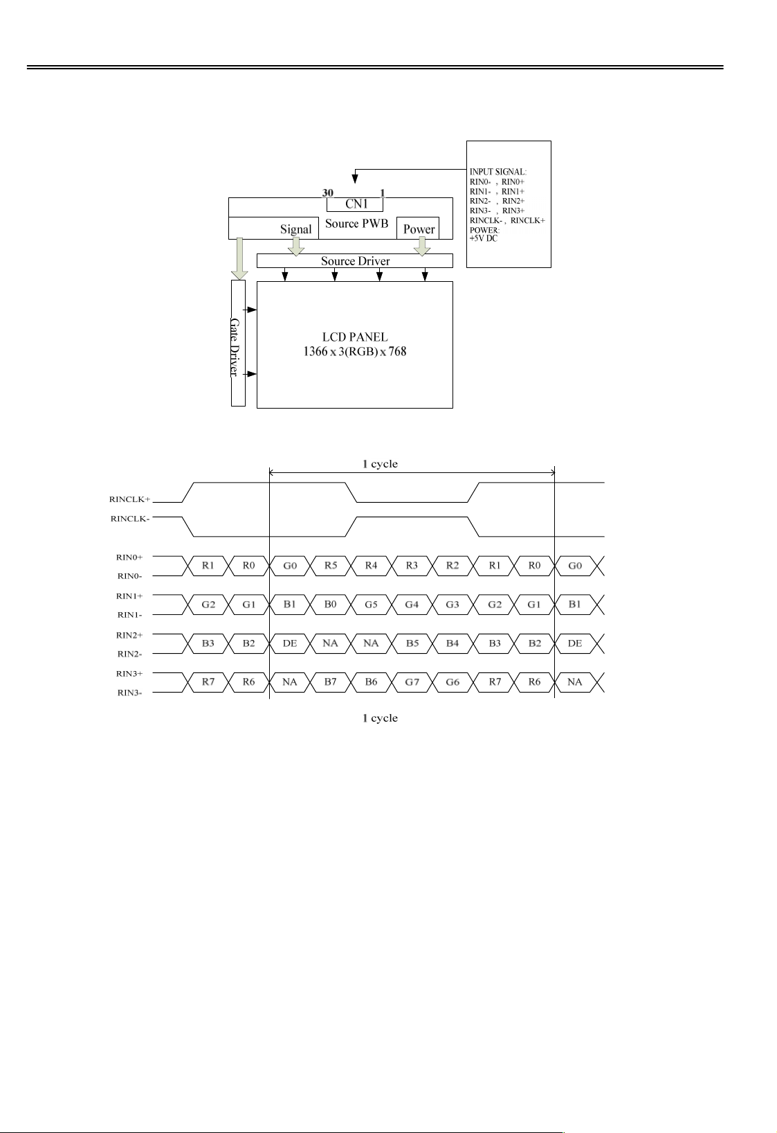
4.2 BLOCK DIAGRAM (OPEN-CELL)
4.3 LVDS INTERFACE
LC185TT2A Specification Version1.1
DE: Display Enable
NA: Not Available (Fixed Low)
R/G/B Data 7:MSB , R/G/B Data 0:LSB ,
9
Page 10
PANDA
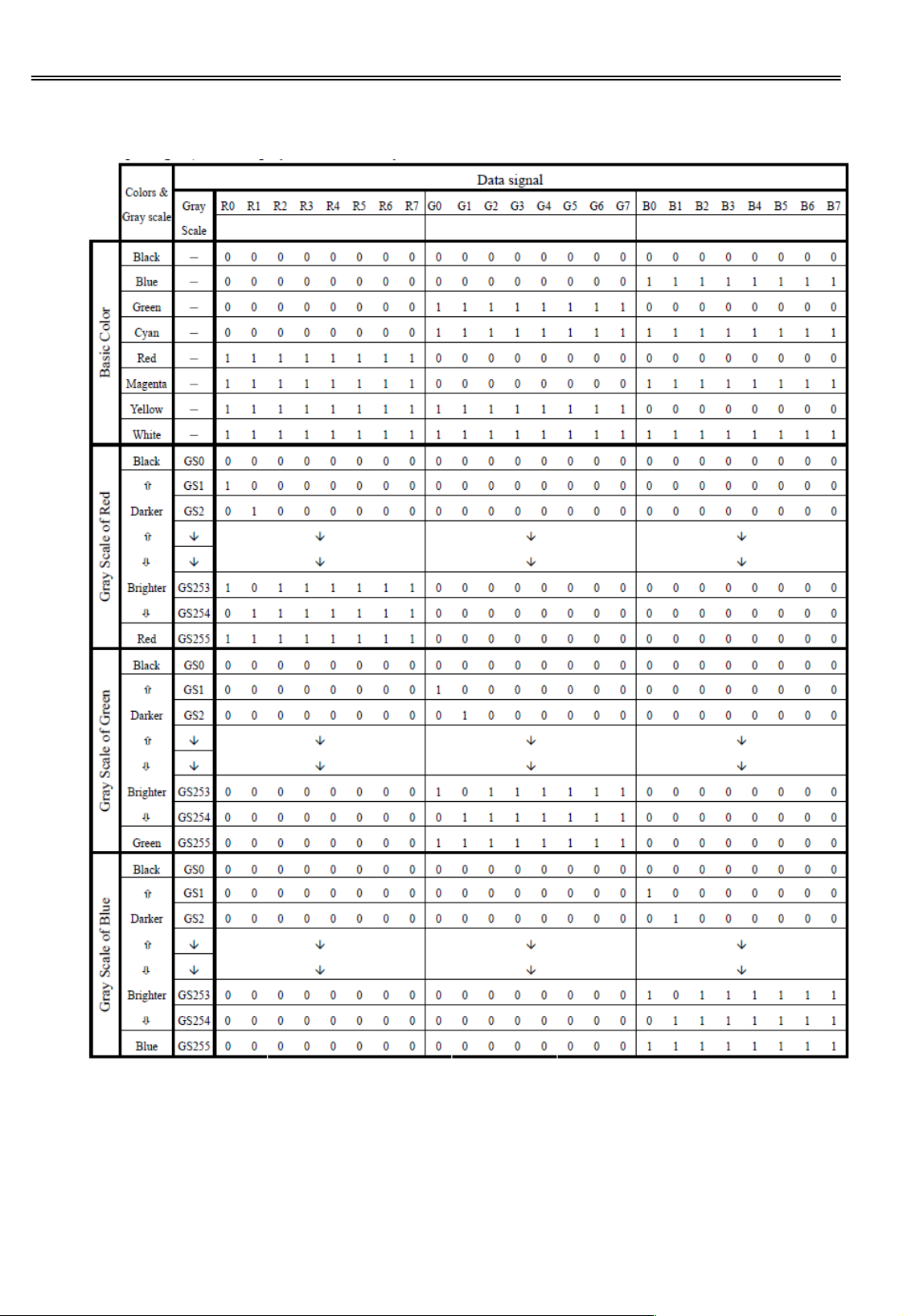
4.4 COLOR DATA INPUT ASSIGNMENT
LC185TT2A Specification Version1.1
0: Low level voltage,
1: High level voltage.
Each basic color can be displayed in 256 gray scales from 8 bit data signals. According to the combination of
total 24 bit data signals, the 16,7M colors display can be achieved on the screen.
10
Page 11

PANDA
Item
Symbol
Min
Typ.
Max.
Unit
LCD
Timing
DCLK
Freq.
fCLK
507695
MHz
Cycle
tCLK
10.5
13.220ns
DE
Horizontal
Horizontal effective time
tHA
1366
1366
1366
tCLK
Horizontal blank time
tHB80200
570
tCLK
Horizontal total time
tH
1446
1560
1936
tCLK
Vertical
Vertical frame Rate
Fr506075Hz
Vertical total time
tV
778
806
888
tH
Vertical effective time
tVA
768
768
768
tH
Vertical blank time
tVB1038
120
tH
LC185TT2A Specification Version1.1
5. INTERFACE TIMING
5.1 INPUT SIGNAL TIMING SPECIFICATIONS
(a) The input signal timing specifications are shown as the following table and timing diagram.
[Note]
*1) DE (data enable) usually is positive
*2) DCLK still inputs during blanking
*3) DE mode only
*4) It maybe cause flicker at Fr=50Hz.
(b) Timing Chart
11
Page 12
PANDA
Parameter
Symbol
Condition
Min.
Typ.
Max.
Unit
Remark
Viewing
angle range
Horizontal
θ
21+θ22
CR>10
-90-
Deg.
[Note1,4]
Vertical
θ
11+θ12
-65-
Deg.
Contrast ratio
CR
=0 deg.
-
600--
[Note2,4]
Response time
Tr+Tf-5-ms
[Note3,4]
Chromaticity of white
x
0.283
0.313
0.343
-
[Note 4]
y
0.299
0.329
0.359
-
Chromaticity of red
x
0.612
0.642
0.672
-
y
0.317
0.347
0.377
-
Chromaticity of green
x
0.284
0.314
0.344
-
y
0.603
0.633
0.663
-
Chromaticity of blue
x
0.128
0.158
0.188
-
y
0.032
0.062
0.092
-
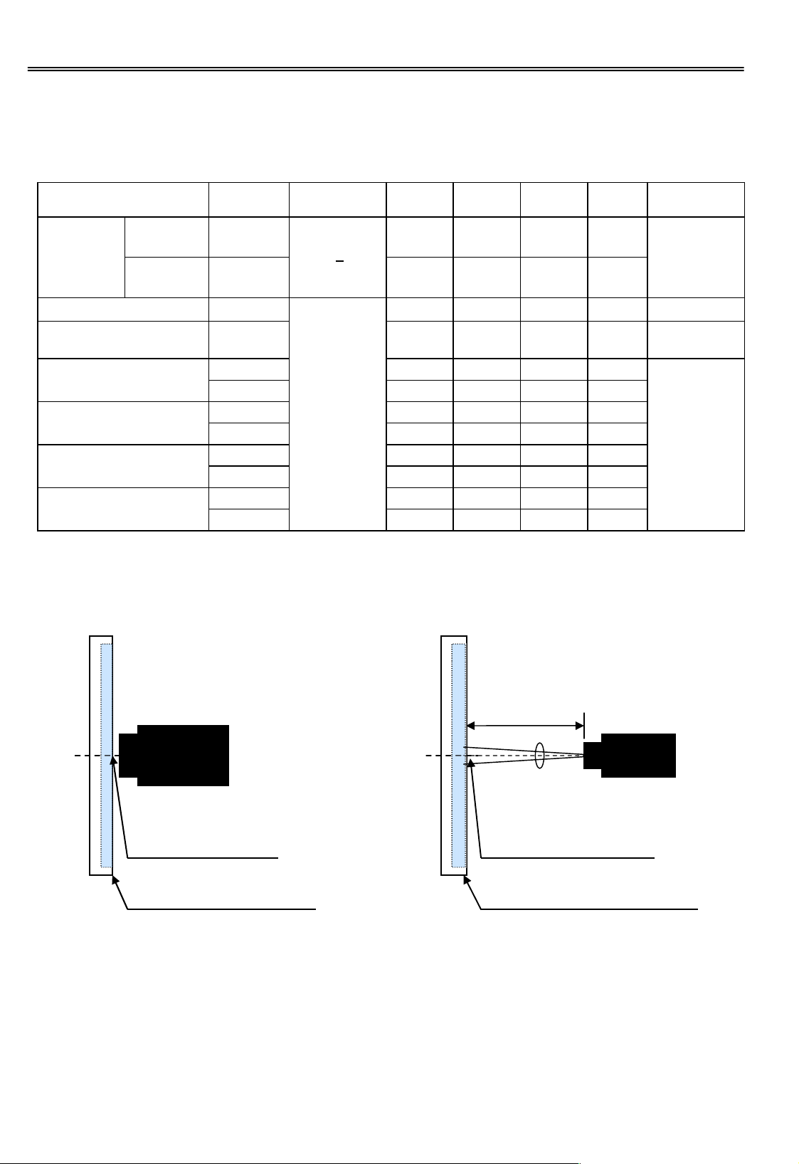
Measurement of viewing angle range, Response time.
Measurement of Contrast, Luminance, Chromaticity.
Middle of the screen (=0)
TFT-LCD Module
Middle of the screen (=0)
TFT-LCD Module
500mm
Field=2
Detector(SR-3)
Detector(EZ-CONTRAST/Photodiode)
6. OPTICAL CHARACTERISTICS
6.1 OPTICAL SPECIFICATION
LC185TT2A Specification Version1.1
Ta=25C
*The measurement shall be executed 30 minutes after lighting at rating.
*These values are measured with CPL standard back light unit.
* The optical characteristics are measured using the following equipment.
12
Page 13
PANDA
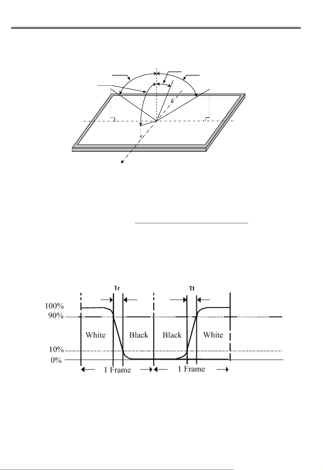
Normal line
21
11
12
22
6 o’clock direction
Contrast Ratio =
Luminance (Brightness) with black screen
Luminance (Brightness) with white screen
[Note 1] Definitions of viewing angle range:
LC185TT2A Specification Version1.1
Viewing angle
[Note 2] Definition of contrast ratio:
The contrast ratio is defined as the following.
[Note 3] Definition of response time
The output signals of photo detector are measured when the input signals are changed from “Full White” to
“Full Black” (rising time, Tr), and from “Full Black” to “Full Black” (falling time, Tf), respectively. The response
time is interval between the 10% and 90% (1 frame at 60 Hz) of amplitudes.
[Note 4] This shall be measured at center of the screen.
Response time=Tr+ Tf
13
Page 14

PANDA
PANDA
QUANTITY : XX
RoHS
DATE:YYYY/MM/DD
MADE IN CHINA
Production date (YYYY/MM/DD)
Model No.
Barcode
Box ID
Quantity
Model No.
Serial number
Production date (YYYY/MM/DD)
Barcode
7. DEFINITION OF LABELS
7.1 LABEL
The label of displays, product model (LC185TT2A), and product label is stuck on the front side of the Open-cell.
7.2 BOX LABEL
LC185TT2A Specification Version1.1
14
Page 15

PANDA
(a)Piling number of EPS BOX
: 24PCS
:TBD
(b)Packing quantity in one ESP BOX
: 20PCS
: TBD
(c)EPS BOX size
: 594×405×143
: TBD
(d)Pallet size
: 1214×845×150
: TBD
(e)Total mass of one EPS BOX filled with full Panel
: 9.95KG
: TBD
Cover Sheet Kraft
Opencell/Multicell20
Packing Band PP2
Corner Attachment LDPE-2
EPS Box Body
Protection Sheet21
EPS Box Cover
Pallet Wood
1214×845×150
Stretching Film
Corner Attachment LDPE-2
Packing Band PP2
Cover Sheet Kraft
Corner Protector Kraft
Corner Protector Kraft
Corner Protector Kraft
8. PACKING
8.1 PACKING SPECIFICATIONS
8.2 PACKING METHOD
LC185TT2A Specification Version1.1
15
Page 16

PANDA
item
Management standard value and performance standard
1
Anti-static mat(shelf)
1to50 [Mega ohm]
2
Anti-static mat(floor, desk)
1to100 [Mega ohm]
3
Ionizer
Attenuate from ±1000V to ±100V within two seconds.
4
Anti-static wrist band
0.8 to 10 [Mega ohm]
5
Anti-static wrist band entry and ground resistance
Below 1000 [ohm]
6
Temperature
22 to 26 [℃ ]
7
Humidity
60 to 70 [%]
LC185TT2A Specification Version1.1
9. PRECAUTIONS
(a) Because the Open-Cell is too weak to destroy by static electricity, please don’t touch the terminal with bare
hands.
(b) Front polarizer can easily be damaged. Pay attention on it
(c) Since long contact with drops of water may cause discoloration or spots, please wipe off them as soon as
possible.
(d) When the panel surface is soiled, wipe it with absorbent cotton or other soft cloth.
(e) The Panel will be broken or chipped when it is dropped or bumped against a hard substance.
(f) Precautions of peeling off the Protection Film:
*1) Be sure to peel off slowly (recommended more than 7 sec.) and constant speed.
*2) Peeling direction shown in the next Fig.
*3) Be sure to ground person with adequate methods such as the anti-static wrist band.
*4) Be sure to connect PWB to GND while peeling off the protection film.
*5) Ionized air should be blown to the surface while peeling off the protection film.
*6) The protection film must not touch drivers and PWB.
After the protection film has been peeled off, some adhesive may be remained on the polarizer. Please
use isopropyl-alcohol to remove it.
(g) Since the Open-cell consists of TFT and electronic circuits with CMOS-ICs, which are very weak to
electrostatic discharge, persons who are handling an Open-Cell should be grounded though adequate
methods such as an anti-static wrist band. Connector pins should not be touched directly with bare hands.
(h) Avoiding COF damage, do not bend PWB to display side when handling the open cell, recommend coating
silicon or tuffy on front and back side of COF.
Reference: Process control standard of CPL.
16
Page 17

PANDA
Test item
Condition
High temperature storage test
Ta= 60C, 240h
Low temperature storage test
Ta=-20C, 240h
High temperature and high humidity
storage test
Ta= 50C, 80%RH, 240h
(No condensation)
High temperature operation test
Ta= 50C, 240h
Low temperature operation test
Ta= 0C, 240h
ESD(no operation)
Contact discharge on LVDS connector
±200V(200PF,0Ω)
(i) Since the Open-cell has a PWB, please take care to keep it off any stress or pressure when handling or
installing the Open-cell, otherwise some of electronic parts on them may be damaged.
(j) Be sure to turn off the power supply when inserting or disconnecting the cable.
(k) Be sure to design the module and cabinet so that the Open-cell van is installed without any extra stress such as
warp or twist.
(l) When handling and assembling Open-Cell into module, please be noted that long-term storage in the
environment of oxidization or deoxidization gas and the use of materials such as reagent, solvent, adhesive,
resin… etc, which generate these gasses, may cause corrosion and discoloration of the Open-Cell.
(m) Applying too much force and stress to PWB and drivers may cause a malfunction electrically and
mechanically.
(n) The Open-cell has high frequency circuits. Sufficient suppression to EMI should be done by system
manufactures.
(o) Please be careful since image retention may occur when a fixed pattern is displayed for a long time.
(p) The chemical compound, which causes the destruction of ozone layer, is not being used.
LC185TT2A Specification Version1.1
(q) This Open-Cell module is corresponded to RoHS.
(r) When any question or issue occurs, it shall be solved by mutual discussion.
10. Reliability test items
[Result evaluation criteria]
Under the display quality test condition with normal operation state, there shall be no change, which may affect
practical display function.
11. Mechanical Drawing
17
Page 18

PANDA
LC185TT2A Specification Version1.1
18
 Loading...