

Panasonic of North America SC HTB8 User Manual
®
Product Specification
Features:
z Bluetooth Spec 4.0 Compliant
z Class 2 type Output Power
z Support A2DP 1.2,AVRCP V1.4 Profiles
z Secure simple pairing, CSR's proximity pairing
and CSR's proximity connection
z Support for multi-language programmable audio
prompts
z OS battery status monitoring and smart apps
z Wired audio support (USB and analogue)
z SBC, MP3, and AAC decoder support
z 5-band fully configurable EQ
z Integrated dual switch-mode regulators, linear
regulators and battery charger
z Size: 21±0.5mm x 13.5±0.5 mm x 2.35±0.5mm
z Weight: 0.8g
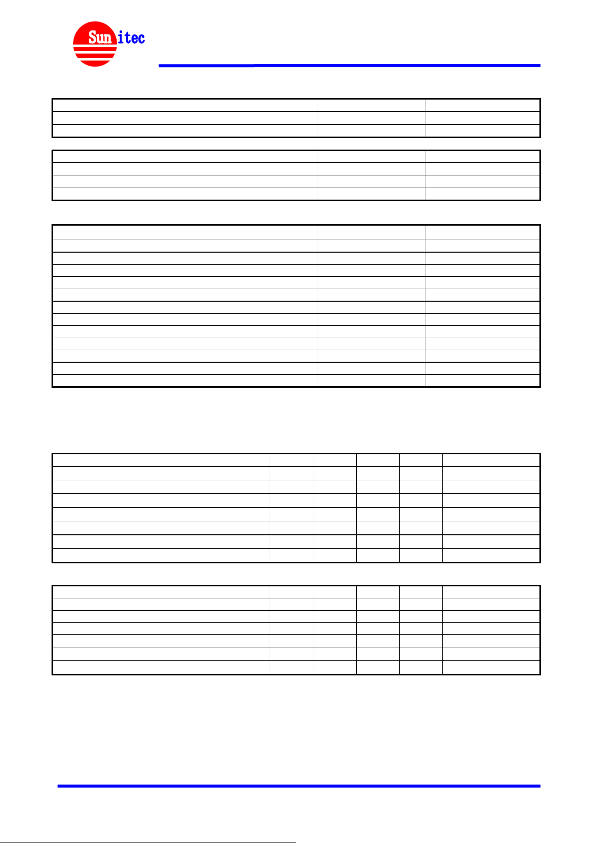
BM830 Stereo Solution Module
CSR
Product Description:
The BM830 is a Class 2 Bluetooth sub-system
using CSR8630 chipset from leading Bluetooth
chipset supplier Cambridge Silicon Radio.
It is a single-chip radio and baseband IC for
Bluetooth 2.4GHz systems.The integrated
peripherals reduce the number of external
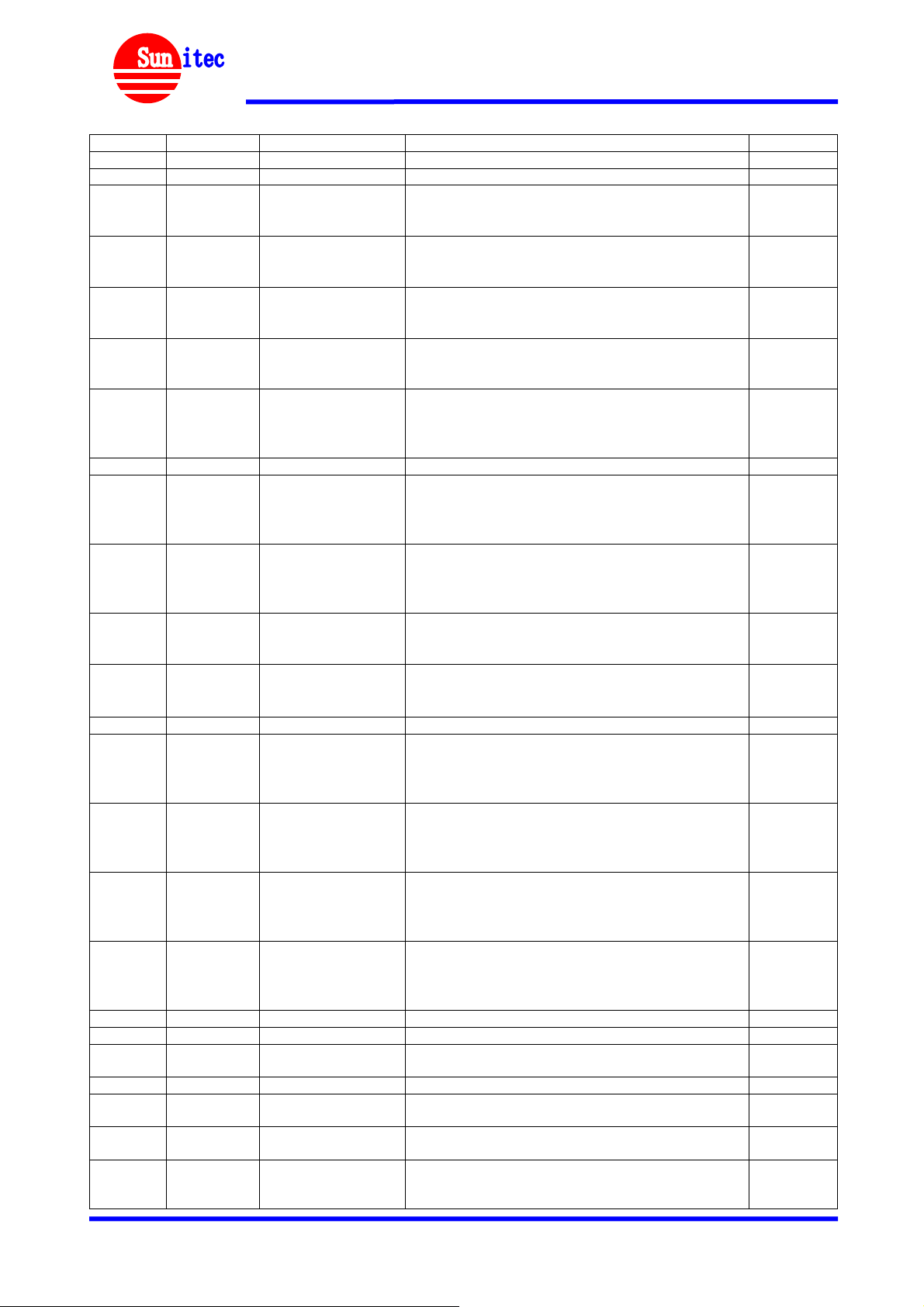
System Architecture
components required, including no
requirement for external codec, battery charger,
SMPS, LDOs, balun or external program
memory, ensuring minimum production costs.
Applications:
• Wireless speaker
Specifications:
Operating Frequency Band
Bluetooth Specification V4.0
Output Power Class Class 2
Max. Output Power 2.5mW
Date Rate 3Mbps
Channel No. 79
Modulation Type GFSK π/4 DQPSK 8DPSK
Operating Voltage 3.3V
Host Interface USB 1.1
Audio Interface Analogue and USB audio
Dimension
Specifications are subject to change without prior notice
2.4GHz ~ 2.48GHz unlicensed ISM band
21±0.5mm x 13.5±0.5 mm x 2.35±0.5mm
July 2013
Qualified
8630A04
Spec-BM830-V0.2 Page 1 of 10 www.sunitec-cn.com
®
Product Specification
Electrical Characteristics
Absolute Maximum Rating Min Max
Storage Temperature
Supply Voltage, (V_CHG) -0.30V +5.75V
Recommended Operating Conditions Min Max
Operating Temperature Range
Supply Voltage, (V_BAT) 2.5V 4.2V
Supply Voltage, (V_CHG) 4.75V 5.25V
Power Consumption Units
Slave
SCO Connection HV3 mA 11.0
SCO Connection EV3 mA 11.8
SCO Connection 2EV3 mA 9.2
Stereo high quality SBC mA 13.3
Stereo high quality MP3 mA 12.5
Master
SCO Connection HV3 mA 10.8
SCO Connection EV3 mA 11.2
SCO Connection 2EV3 mA 8.8
Stereo high quality SBC mA 13.2
Stereo high quality MP3 mA 11.8
VBAT = 4.2V; f = 2.441GHz; T=20°C
RF Characteristics
Receiver Units Min Typ Max Bluetooth Spec
Sensitivity at 0.1% BER dBm - -90 -85
Maximum Receiver Signal dBm -20 -10 C/I Co-Channel dB - 6 11
Adjacent Channel Selectivity C/I -1MHz dB - -6 0
2nd Adjacent Channel Selectivity C/I -2MHz dB - -38 -30
3rd Adjacent Channel Selectivity C/I -3MHz dB - -45 -40
Image Rejection C/I dB - -16 -9
VBAT = 4.2V; f = 2.4441GHz; T=20°C
Transmitter Units Min Typ Max Bluetooth Spec
RF Output Power dBm 4 8 - -6 to +4
RF Power Control Range dB 16 24 - > 16
RF Power Range Control Resolution dB - 0.5 - 20dB Bandwidth for Modulated Carrier KHz - 940 1000 <1000
2nd Adjacent Channel Power (+/- 2MHz) dBm - -36 -20
3rd Adjacent Channel Power (+/- 3MHz) dBm - -45 -40
VBAT = 4.2V; f = 2.4441GHz; T=20°C
All specifications including pinouts and electrical specifications may be changed without prior notice
-40°C +105°C
-40°C +85°C
Average
≤-70
≥ -20
≤11
≤0
≤-30
≤-40
≤-9
≤-20
≤-40
Spec-BM830-V0.2 Page 2 of 10 www.sunitec-cn.com
®
Product Specification
Pin Configurations
PIN NO. NAME TYPE FUNCTION RE-MARK
1 GND GND Ground
2 AIO0 Bi-directional Analogue programmable input / output line
3 PIO14 Bi-directional Programmable input / output line 14.
Alternative function:
■ UART_RX: UART data input
4 PIO15 Bi-directional Programmable input / output line 15.
Alternative function:
■ UART_TX: UART data output
5 PIO16 Bi-directional Programmable input / output line 16.
Alternative function:
■ UART_RTS: UART request to send, active low
6 PIO17 Bi-directional Programmable input / output line 17.
Alternative function:
■ UART_CTS: UART clear to send, active low
7 PIO10 Bi-directional Programmable input / output line 10.
Alternative function:
■ QSPI_FLASH_CLK: SPI flash clock
■ I2C_SCL: I²C serial clock line
8 SCL Bi-directional Internal EEPROM SCL
9 PIO11 Bi-directional Programmable input / output line 11.
Alternative function:
■ QSPI_IO[0]: SPI flash data bit 0
■ I2C_SDA: I²C serial data line
10 PIO12 Bi-directional Programmable input / output line 12.
Alternative function:
■ QSPI_FLASH_CS#: SPI flash chip select
■ I2C_WP: I²C bus memory write protect line
11 PIO13 Bi-directional Programmable input / output line 13.
Alternative function:
■ QSPI_IO[1]: SPI flash data bit 1
12 SPI_PCM# Bidirectional with
weak
pull-down
13 GND GND Ground
14 PIO3 Bi-directional Programmable input / output line 3.
15 PIO2 Bi-directional Programmable input / output line 2.
16 PIO5 Bi-directional Programmable input / output line 5.
17 PIO4 Bi-directional Programmable input / output line 4.
18 GND GND Ground
19 GND GND Ground
20 RST# Input with strong
pull-up
21 GND GND Ground
22 LED1 Bi-directional LED driver.
23 LED0 Bi-directional LED driver.
24 VREGENA
BLE
CMOS Input Regulator enable input
SPI/PCM select input:
■0 = PCM/PIO interface
■1 = SPI
Alternative function:
■ SPI_MISO: SPI data output
■ PCM1_OUT: PCM1 synchronous data output
Alternative function:
■ SPI_MOSI: SPI data input
■ PCM1_IN: PCM1 synchronous data input
Alternative function:
■ SPI_CLK: SPI clock
■ PCM1_CLK: PCM1 synchronous data clock
Alternative function:
■ SPI_CS#: chip select for SPI, active low
■ PCM1_SYNC: PCM1 synchronous data sync
Reset if low. Pull low for minimum 5ms to cause a
reset.
Alternative function: programmable output PIO[30].
Alternative function: programmable output PIO[29].
Can also be sensed as an input.
Regulator enable and multifunction button. A high
Spec-BM830-V0.2 Page 3 of 10 www.sunitec-cn.com
 Loading...