

Page 1
Technical Guide
Colour Television
Z8 Chassis
Circuit Explanations
7*
Panasonic
(XURSHDQ 7HOHYLVLRQ 'LYLVLRQ
0DWVXVKLWD (OHFWULF 8. /WG
Page 2

3DQDVRQLF
CONTENTS
1. Introduction 3.........................................................
2. Block Diagrams 4.....................................................
3. Power Supply 8.......................................................
4. TV Signal, Control and Teletext Processing 15.............................
5. Horizontal Output 28....................................................
6. Vertical Output 29......................................................
7. East-West Correction 30................................................
8. Memory (EEPROM) 31.................................................
9. Colour Output 32.......................................................
10. MSP3415D Audio Signal Processing 34...................................
11. AF Output Stage 41....................................................
12. Appendices 42.........................................................
Page 3

1. Introduction
3DQDVRQLF
We at Panasonic realise that the service engineer
needstounderstandthecircuitry insidetheTVandfor
this need, we have produced this Technical Guide.
This Technical Guide contains information for Z8
chassis and should be used in conjunction with the
relevant Service Manuals for this chassis.
Page 4
3DQDVRQLF
2. Block Diagrams
2.1. Control Block Diagram
<
Page 5
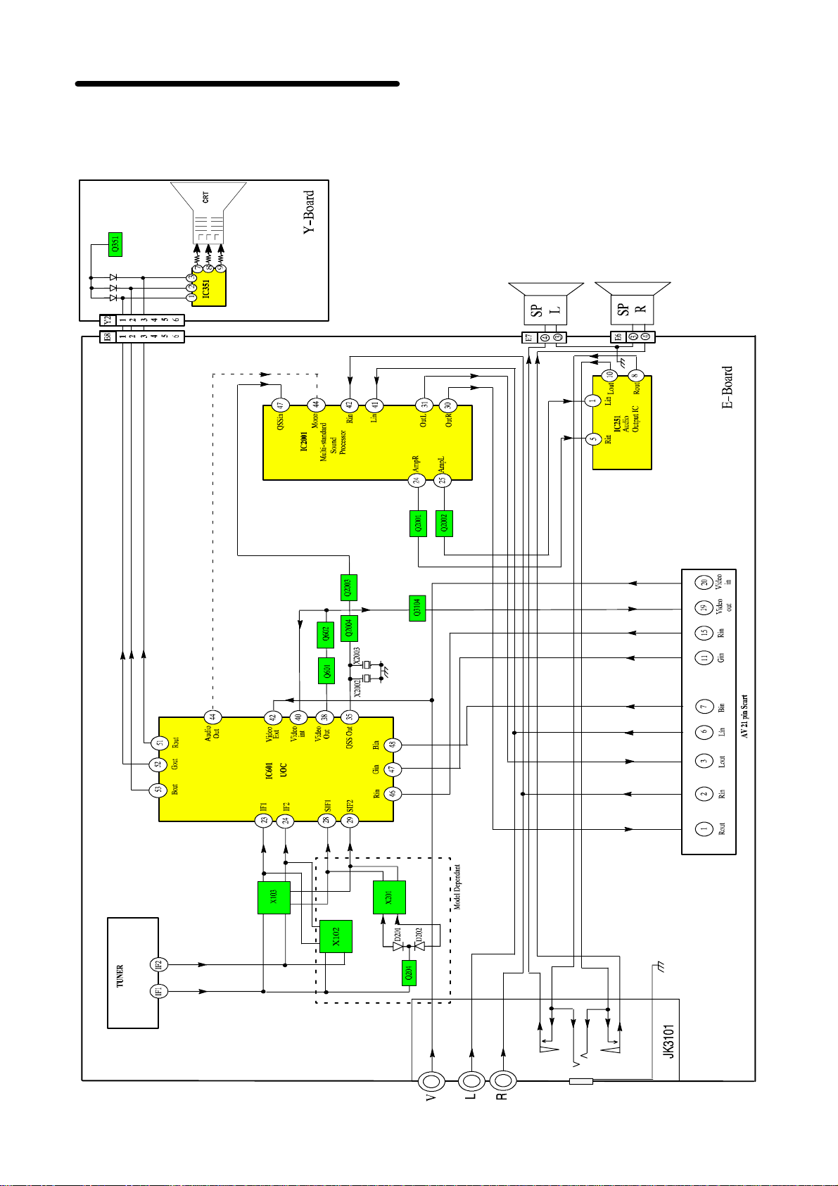
2.2. Power Supply and Deflection Block
Diagram
3DQDVRQLF
<
<
9
(
(
(
Page 6
3DQDVRQLF
2.3. Video and Mono Audio
Block Diagram
Page 7
2.4. Video and Stereo Audio
Block Diagram
3DQDVRQLF
Page 8
3DQDVRQLF
3. Power Supply
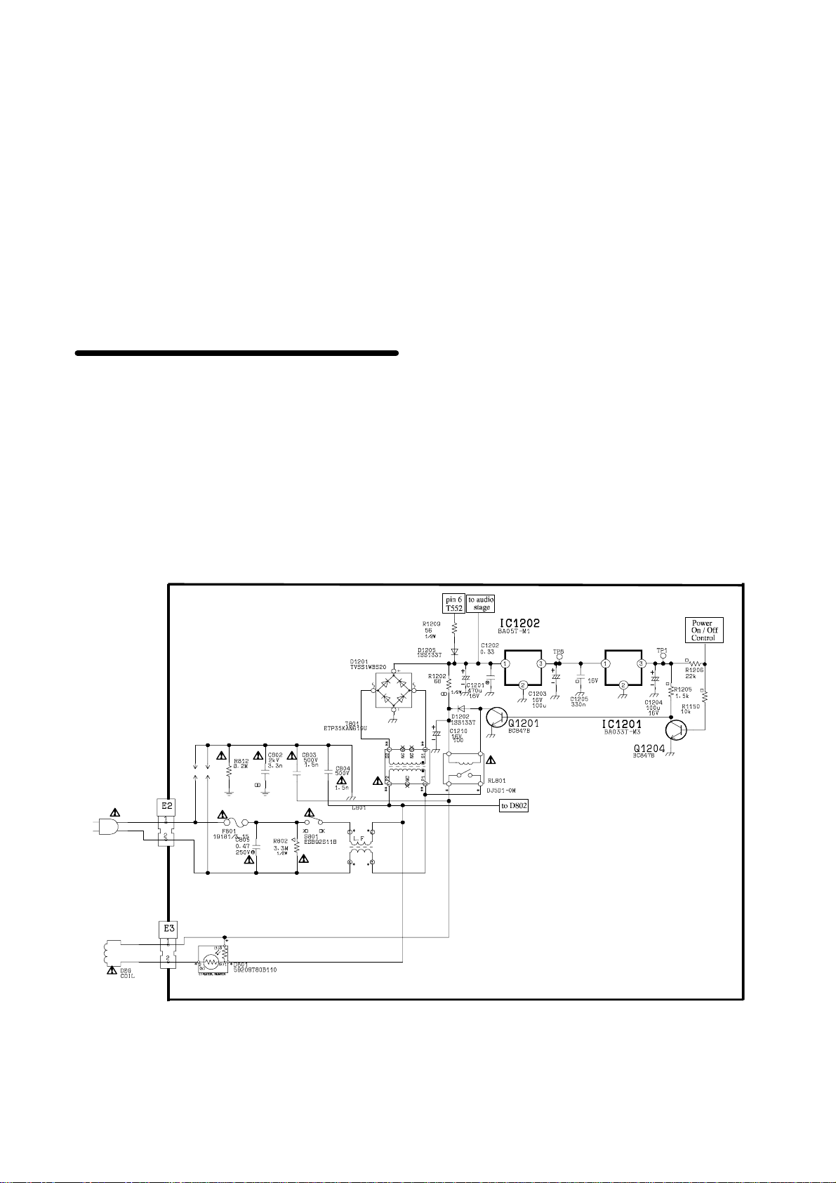
ThemainsACvoltageusedforZ8isfed viaconnector
E2 situated on the E-Board. From the connector E2
the mains AC power supply is fed via the main TV
On/Off switch S801 and line suppression filter L801
before being fed to the standby transformer T801.
At the standby transformer T801 the AC supply splits
into two paths.
The first path sees the AC supply being fed to the
normally open contact of the standby relay RL801.
The second path has the AC supply being fed viathe
windings P2/P1 of the standby transformer T801.
3.1. Standby Power Supply Circuit
The standby transformer T801 has the AC supply as
just mentioned being fed via the primary winding
P2/P1.
The output of the secondary windings S2/S1 of the
standby transformer is fed to the bridge rectifier
D1201,where theACvoltage is fullrectified. Herethe
supply takes two paths.
The first path provides smoothing to the supply via
capacitor C1201 before being fed to IC1202 pin 1.
The output at pin 3 is smoothed further by capacitor
C1203,and the 5Vstandby supply output is fedto the
EEPROM IC1103, the remote control receiver
IC1104and theQ-Link circuit. The5V standby supply
is also fed to IC1201, where the output at pin 3 is
smoothed viaC1204, to provide3.3V standby supply
to theUltimateOne Chip(UOC) IC IC601 pin 61, and
thereset ICIC1102.This3.3V isalso usedto bias the
standby relay control transistor Q1204.
The second path from the bridge rectifier sees the
supply voltage being fed via resistor R1202 to the
standby relay RL801 and the relay winding to the
collector of transistor Q1201. Transistor Q1201,
which is controlled by Q1204, is responsible for
switching the TV in and out of standby, under the
control of the UOC IC IC601 pin 1.
The two supplies mentioned allow the circuits to
operate during standby, which is required to process
the switch ON command from the remote control or
local keys, allowing the TV to be switched out of
standby.
To reduce the load on the standby transformer T801,
a 10V supply is fed from transformer T552 pin 6 via
rectifying diode D554, R1209 and D1205, to pin 1 of
IC1202.
Page 9
3DQDVRQLF
3.2. Power Supply Circuit
The STR-F6523, IC801 is used in the Z8 power
supply to control and regulate the power supply
operation. This device features over-voltage
protection and thermalshutdown.The output stageof
the IC incorporates a built-in MOSFET switching
transistor.
3.3. Operation
The supply voltage for the main power supply circuit
is fed via the standby relay RL801 to the bridge
rectifier D802 where the AC voltage is fully rectified
and smoothed by capacitor C809.
This smoothed DC voltage of approximately 300V
then feeds the supply to pin 3 of the switched mode
power supply IC IC801, wherethe DC voltage is held
at the drain of the internal MOSFET, by its parallel
zener diode.
Page 10
3DQDVRQLF
3.4. Start Up
A start-up circuit is used to start and stop the
operations of the control IC IC801 (STR-F6523), by
detecting the voltage appearing at the V
pin 4.
At start-up, capacitor C810 is charged via R804,
which causes the voltage at pin 4 of IC801 to
increase. Once V
terminal pin 4 voltage reaches
IN
approximately 16V,IC801beginstooperateanddrive
the internal power MOSFET, causing current to flow
through the drain/source terminals at pins 3 and 2,
and to the winding B1-B2 of switching transformer
$&
LQ
terminal,
IN
T802 via L803 and R809. The current at terminal B1
is split into two paths.
The first path follows the current being fed to the
winding B1-B2 and back to pin 4 of IC801 via R811
and D805. Once the control circuit starts operation,
the voltage at the V
terminal pin4 of IC801 starts to
IN
decrease. However, the drive winding voltage
reachestheset value before pin 4voltagedropsto the
shutdownvoltageof 10V.Hencethe voltage supplyto
pin 4 is maintained.
The secondpath is connected from terminal B1 toP2
ofthe FBT. Thiscausescurrent toflowvia thewinding
P2-P1,which providesthe+B supply totheFBT T552
pin 9.
$&
LQ
Page 11

3DQDVRQLF
3.5. Oscillator and Constant Voltage
Control Circuit
Theoscillator withinIC801 makesuseof the charging
and discharging of internal capacitor C1 (4700pF)
and generates pulse signals which turn the internal
power MOSFET On and Off. The constant voltage
control of a switch mode power supply is performed
byfixing theOFF timeof theMOSFET (around50uS)
and changing the ON time in the pulse width control
operation.
3.5.1. ’ON’Condition and Time
When the switching power MOSFET is ON, C1
begins to charge.
3.5.2. From ’ON’ to ’OFF’
When the voltage on C1 reaches (approx.) 6.5V, the
output fromthe oscillatoris reversed, and theinternal
switching power MOSFET switches OFF.
3.5.3. ’OFF’Condition and Time
With the power MOSFET now OFF, Capacitor C1
starts discharging through R1, at the fixed time
determined by the time constant C1, R1.
3.5.4. From ’OFF’to ’ON’
When C1 voltage has dropped to around 3.7V, the
output from the oscillator is reversed again and the
power MOSFET again turns ON, thus repeating the
cycle.
Page 12
3DQDVRQLF
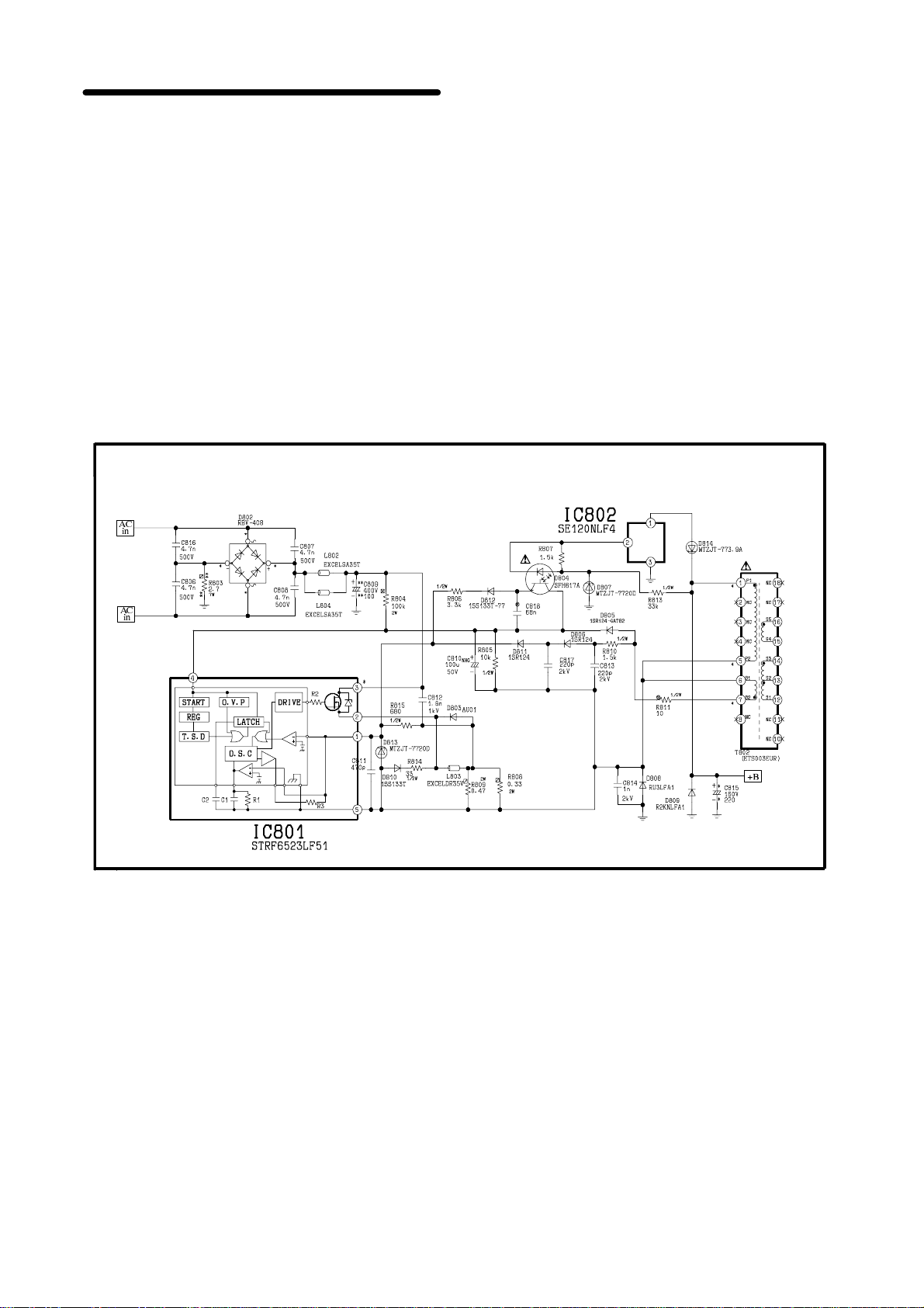
3.6. Regulation
The power supply ON time is changed by controlling
the the charge current of the internal capacitor C1.
D804 is a photocoupler, which provides the drive
current to the ’FB’ (Feedback) terminal of IC801 pin
1 via D812 and R806. The photocoupler current
varies in response to the output from pin 2 of
comparator IC IC802.
IC802 pin 1 monitors the +B supply voltage via the
zener diode D814 by comparing it with a reference
voltage established internally within IC802.
If the AC mains input voltage to the switched mode
power supply increases, the+B voltagelevel tendsto
rise.This results in anincreased currentflowtotheFB
terminal, pin 1 of IC801 via the photocoupler D804,
diode D812 and resistor R806. Increasing the rate at
which C1 charges, causes the power MOSFET ON
time to reduce. This in turn causes the +B level to
return to its nominal value.
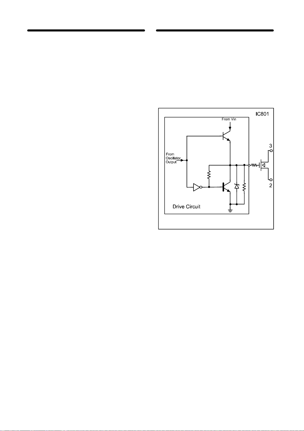
3.7. Drive Circuit
The drive circuit charges and discharges the
capacitance between the gate and the source
terminals of theinternalpowerMOSFET, by receiving
pulses from the oscillator. The basic circuit
configuration is a totem-pole type connection of
transistors. Since the maximum sink current (0.3A)
canbecomeactiveevenwhentheV
than the shutdown voltage, the drive circuit turns off
the MOSFET without fail.
voltageislower
IN
Page 13

3.8. Protection Circuitry
3.8.1. Over-voltage Protection (OVP)
Over-voltageProtectionisusedtoprotect IC801 if V
pin 4 terminal rises to approximately 22V. Although it
basically functions as protection for pin 4 against
overvoltage, it is also used to protect against
overvoltage of the secondary output (in the event of
failureofthe regulation,for example).This is because
pin 4 is supplied by winding B1-B2 of transformer
T802, this voltage being proportional to the output
voltage of the secondary side.
3DQDVRQLF
IN
16V
10V
t
3.8.2. Over-current Protection (OCP)
Overcurrent Protection is performed pulse-by-pulse
by directly detecting the drain current of the internal
power MOSFET. Since the detection voltage is
monitored by an internal comparator of IC801,
constant temperature stabilisation is also achieved.
The Drain-Source current through the power
switching MOSFET is passed via the resistor R809,
which developsa voltage across it. The input voltage
to IC801 pin 1 (OCP/FB) is passed to an internal
comparator. When this input voltage exceeds a
pre-determined value,the driveoutputis pulled LOW,
resulting in the power MOSFET switching OFF .
3.8.3. Latch
The latch circuit is used to pull the output of the
oscillator LOW (switching MOSFET OFF) when the
over-voltage protection or thermal shutdown circuits
are activated.
In this condition the VINterminal pin4decreases until
the shutdown voltage of 10V is reached. At this point
pin4begins torise again but whenitreaches thestart
up level of 16V, the latch circuit continues to stop the
drive.
When the latch is on, V
anddecreases withinthe range 10Vto16V,asshown
in the above diagram, and is prevented from rising
normally.
Cancellation of the latch circuit operation is achieved
by restarting the AC input tothe circuit afterswitching
off the TV.
3.8.4. Thermal Shutdown
This circuit triggers the latch when the body
temperature of the IC exceeds 140
temperature is sensed by the control IC, but also
works against overheating of the MOSFET, as both
are mounted on the same lead frame.
voltage at pin 4 increases
IN
E
C. The
Page 14

3DQDVRQLF
3.9. Secondary Supplies
On the secondary side, the transformer T802
supplies the following voltages:
: +12V to supply the horizontal driver stage.
: +20V to supply the East/West correction IC
IC701.
: +27V to supply the audio output IC IC251.
3.9.1. +12V Supply
The signal from pin 16 of T802 is rectified by diode
D851 and smoothed by capacitor C856. The 12V
supply voltage is then applied to the horizontal driver
transformer T553 via diode D501 and resistor R503.
During start-up, the 12V supply feeds the horizontal
stageas mentioned. However,whenthewholepower
supply is up and running normally,the supply voltage
fromthesecondary of T802isnolongerrequired. The
horizontal stage now takes its 12V supply from the
FBT T552. This is required to reduce the load on the
secondary and provide drive current to thehorizontal
driver transformer T553.
3.9.2. +20V Supply
The signal from pin 14 of T802 is rectified by diode
D853 and applied to the series regulator IC702 to
supply +20V to the East/West circuit (model
dependant).
3.9.3. +27V Supply
The signal from pin 14 of T802 is rectified by diode
D853 and applied to the emitter terminals of
transistors Q851 and via resistor R855 to Q852. This
voltage to Q852 is fed via the emitter/collector
junction. At the same time, the signal from pin 13 of
T802 is rectified by diode D852 to provide a voltage
of +27V, which is fed to the audio output IC IC251.
This supply voltage of +27V however is too large for
theabove mentionedICs whenunder load and sothe
supply voltage has to be reduced. As the load on the
above ICs increases, the voltage drop across R856
increases causingthe baseof Q851 to become more
negative with respect to its emitter. With Q851
conducting the base bias of Q852 becomes more
positive with respect to its emitter, thus causing the
supply voltage to the ICs to be reduced.
Howeverby reducingthe supply voltagetoIC251, the
output power is also reduced. This is compensated
forbytheincreased current flowviaR853/ R854.This
in turn ensures that the output power of theICs is not
affected.
3.10. Voltage Supplies
3.10.1. +12V Supply
The +12V supply is output from transformer T552 pin
4andis rectified by diodeD553. This rectifiedvoltage
issmoothedbycapacitorC566before beingfedto the
vertical output IC IC451 pin 6. The +12V supply also
feedsthehorizontaldriver transformer T553 viadiode
D510 and resistor R503.
3.10.2. -12V Supply
The -12V supply is output from transformer T552 pin
5andisrectifiedbydiodeD559.This negativevoltage
issmoothedbycapacitorC564before beingfedto the
ground terminal pin 1 of the vertical output IC IC451.
3.10.3. +10V Supply
A supply of approximately 10V is output from
transformer T552 pin 6, and fed to diode D554. This
rectified voltagesignal isthen smoothed bycapacitor
C554 before being fed to the series regulator IC852
and the standby voltage regulator IC1202.
3.10.4. +8V Supply
The 8V supply is derived from the 10V supply line
which is fed to the series regulator IC852 pin 1. The
output of IC852 pin 3, smoothed by capacitor C857,
is used to supply 8V to the TV control processor IC
IC601, RGB output stage (Y-Board) via connectors
E8 and Y2 pin 6, sound processor IC2001 and
SECAM IF audioswitching IC IC201 (French models
only). IC852 also supplies the 5V series regulator IC
IC851.
3.10.5. +5V Supply
The 5V supply is derived from the 8V supply line
which is fed to IC851 pin 1. The output at pin 3,
smoothed by capacitor C851, is used to supply 5V to
the tuner, reset IC IC1105 and the sound processor
IC2001 (model dependant).
Page 15
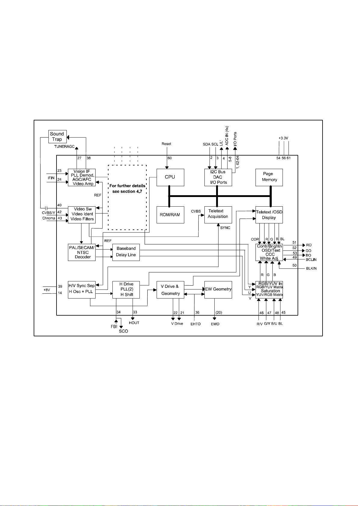
4. TV Signal, Control and Teletext Processing
3DQDVRQLF
The TDA9350/60/80 series IC601 used on Z8
chassis, is a one chip solution in TV processing. The
Philips Ultimate One Chip (UOC) IC combines the
functions of a TV signal processor and teletext
decoder as well as an embedded microcontroller
used to perform control processing. The TV signal
and teletext processing stages will be looked atlater.
First, the control processing stage of the UOC IC will
be examined.
Page 16

3DQDVRQLF
4.1. Control Processing Stage
Theelementsthatthe UOC IC requiredtoperform the
control functions are:
: 80C51 microcontroller
: 12MHz internal clock
: 32 - 128K x 8 bit late programmed ROM
: 3 - 12K x 8 bit Auxiliary RAM
allows composite video and RGB signal input. Slow
switchingbeingprovidedviapin8for compositevideo
input.
: Pin 36 - EHT / Short Circuit Protection
This input to the UOC IC which is normally biased by
R2202 and R621, provides protection by switching
the TV into standby mode.
: Interrupt controller for individual enable/disable
: Two 16 bit Timer/Counter registers
: WatchDog timer
: Serial Interface
: IDLE and Power Down (PD) mode
: 14 bits Pulse Width Modulation for Voltage
Synthesis Tuning
: 8 bit A/D Converter
: Programmable as general I/O, ADC input or
PWM (6-bit) output
4.1.1. Input Control
: Pin 6 - Keyscan
The localcommands are fed tothe UOC IC IC601as
serial data. This data is inputvia pin6. This pinis held
at 3.3V due to the pull-up resistor R1140, which is
connected to the 3.3V standby supply. This means
that the High level is also maintained during standby
condition. Operating commands fed from the local
keys results in varying voltages being applied to pin
6, which in turn initiates the various controls.
When operating commands are fed via the remote
control topin 64of IC601, pin6 of IC601 also outputs
a pulse, which feedstransistors Q1102and Q1107to
provide a flashing standby LED D1104.
Operating commands issued from the local and
remote control are treated with equal status.
: Pin 8 - Slow Switching
The circuit is designed so that it is possible to switch
over to AV operation from allprogramme locations to
the AVinterface. The A V21 pin scart socket JK3102
Short circuit protection is provided via transistor
Q603. The supply lines which are monitored are:
: +200V supply monitored by D603.
A voltage drop in the +200V supply causes the
voltageacross resistorR631 to decrease.This in
turn causes diode D603 to conduct. The base of
Q603 is held high by resistor R622. The voltage
drop applied to the base of transistor Q603,
causes Q603 to switch On. The protection input
at pin 36 of IC601 is now pulled High, switching
the TV into standby.
: +5V supply monitored by D601.
A drop in the +5V supply is applied to the base
of transistor Q603, causing the transistor to
switchOn. The protectioninputatpin36ofIC601
is pulled High, switching the TV into standby.
In addition to the supplies mentioned above,
protection is provided for the +8V supply, which is
carried out internally within the UOC IC via pins 14
and 39. When the voltage drops below the
pre-determined reference, the TV is switched into
standby mode.
Protection is also provided for the Automatic Beam
current Limiting (ABL) circuit via D403, discussed in
section 9.1.3.
: Pin 49 - Automatic Beam Current Limiting
Beam Current Limiting is performed internally within
the UOCIC IC601, and isused tomonitor thevoltage
at the BCL terminal pin 49. The brightness and
contrast varies in response to the voltage at pin 49 of
IC601.
Thecontrol pathstothe BCL inputpin49 is discussed
in the CATS Eye control section 4.1.2. and Colour
Output section 9.1.3.
Page 17

3DQDVRQLF
: Pins 58 / 59 - XTALIN / XTALOUT
The internal oscillator of the UOC IC is synchronised
with an external 12MHz quartz crystal X601 which is
connected to pins 58 and 59.
Theclock frequenciesfor theI
obtained from this frequency by internal dividing.
The same 12MHz clock signal is also divided down
and used to synchronise the video processing stage.
: Pin 60 - Reset
During power On/Off operation, or during a fall in
voltagetothe UOCIC,incorrect operationmayoccur.
To prevent this incorrect operation, the UOC IC has
a reset signal input via pin 60.
The reset signal is provided by reset IC IC1102 pin 1,
whichkeepsthe UOCIC inastable conditionuntil the
voltage level has risen and become stabilised. This
reset IC IC1102 which is fed a 3.3V standby supply,
is input via pin 2.
: Pin 64 - Remote IN
Thecommands requiredforcontrol oftheTVreceiver
are applied from the remote control.
The command from the remote control transmitter is
applied via IC1104, RPM-637BRS remote control
receiver topin 64of the UOC IC. This command data
is received in serial format.
4.1.2. Output Control
: Pin 1 - Standby
This output port of the UOC IC is used to control the
switching of the TV in and out of standby. The signal
path from this output at pin 1 follows two paths.
The first path is fed via the controlling transistor
Q1204. A Highlevel is applied from pin 1to the base
of transistor Q1204, causing Q1204 to switch On.
This in turn causes Q1201 to switch Off, preventing
current flow via the winding of the standby relay
RL801. This results in the mains AC supply being
removed from the power supply circuit.
Likewisewhen a low levelisfed tothebase of Q1204,
the transistor is biased Off, thus allowing transistor
Q1201 toconduct by a Highlevel which is applied via
R1205. When Q1201 conducts, current via the
standby relay causes the relay contact to close and
feed the mains AC voltage to the power circuit.
The second path is fed via resistor R1141 to the
collector of transistor Q1 109. During standby , the
High level applied from pin 1 to collector Q1109
2
Cbussystemarealso
causes Q1107 to conduct, switching the LED D1104
On.
When an operating command is used either from the
local keys or remote control, the keyscan output pin
6 of IC601 is pulled Low, causing transistor Q1102to
switchOff. Thisresultsinthebaseoftransistor Q1 109
to go High due to pull up resistor R1146, to switch
Q1109 On. Q1110 also conducts pulling the base of
Q1107 Low , thus switching it Off. This results in the
standby LED D1104 switching Off.
: Pin 4 - L/L’
Pin 4of the UOC IC IC601 is used to select between
the two types of SECAM standards L/L’. This control
signal is used on SECAM L models only.
: Pin 5 - CATS Eye
Pin5 of theUOCIC is usedtocontrol a featureknown
as CATS (C
This is used toadjust the contrast leveldepending on
the external lightsurrounding the TV. The level of the
adjustment made is dependant upon the mode
selected via the OSD (Medium / Maximum).
The light sensed by the LDR (Light Dependant
Resistor) R1283 is used to control the conduction of
transistor Q1101 which in turn, controls the voltage
level at pin 49 of IC601 and thus, the contrast level.
: Pin 7 - Neg / Pos
This output control is used to select between
PAL/NTSC (Negative modulation) and SECAM
(Positive modulation) standards selection.
Pin 7 is also used as an input on UK models only, to
achieve thehighest possible signal from thetuner via
Q001.
: Pin 11 - Mute
Themute controlwhich is output from the UOC ICpin
1 1is fed to the audio output IC IC251 pin3 viaQ255.
Pin 11 of IC601 which is pulled Low for normal
operation, is biased by resistor R1141 to the 5V
standby supply.
During channel change, tuning and muting
operations, the Low level output from pin 11 is
disabled causing the base of Q255 to go High,
switching it On. This results in pin 3 of IC251 being
pulled Low,resulting inthe audio output being muted.
Muting is also provided for audio POP during On/Off
operation via transistor Q253, the operation of which
is discussed in section 11.2.1.
ontrast Automatic Tracking System).
Page 18

3DQDVRQLF
4.1.3. Q-Link
: Pin 62 - Q-Link_In / Pin 63 - Q-Link_Out
Q-Link input and output is a model dependant
function used to control the transfer of information
and user functions to and from the TV / VCR via AV
21 pin socket JK3102.
The AV link control line fed from pin 10 of the 21 pin
AV socket is fed to the Q-Link circuit made up of
Q1103, Q1106, Q1 105 and Q1104.
Where data is fed from theTV to the VCR, the Q-Link
output terminal pin 63 of the UOC IC IC601 is used.
This results in the data being fed from pin 63 of the
UOC IC IC601 via Q1106.
Where data is input from the VCR to the TV ,then the
Q-LinkInterminal pin 62 of the UOCICIC601 is used.
This results in data being fed via Q1 103, Q1 105and
Q1104 to the UOC IC IC601 pin 62.
The type of data and function control information fed
via the Q-Link is as follows:
: TV Auto Power ON: TV automatically turns ON
when the VCR starts play-back.
: VCR Auto Standby: VCR will automatically
switch to standby when the TV is turned OFF ,
unless the VCR is in recording mode.
: TV On screen Display of VCR status.
: Download of Country selection.
These above features will only workwith aPanasonic
TV / video combination which are both Q-Link
(Project 50+) compliant.
The features below will work with different brands of
TV and videocombinations, againas long asboth TV
and video are Project 50 compliant.
: Tuner preset data down load (TV->VCR)
: What You See Is What You Record (Direct TV)
In addition to these features the TV/Video also
include in their protocol Automatic signal matching
(signal quality). Here the TV/video at first time of
connecting, exchangeinformation regardingfeatures
andoperationalcapabilities, suchassignalstandards
and the ability to process and display 16:9 format, for
example.
2
4.1.4. I
CBus
: Pins 2 / 3 - SCL / SDA
2
TheI
C bus is a two-wire Bus system consistingof a
data line and a clock line. This BUS system allows
serial and bidirectional communications exchange
2
between several devices which include an I
C bus
interface. The number of connections are therefore
reduced, which results in a simplified circuit design
and increased reliability (less soldered
joints/connections and contacts).
Within the the UOCIC, the microcontroller stage and
the signal processing stage utilise this Bus.
Page 19

3DQDVRQLF
4.2. Colour TV Signal Processing
The TDA9350/60/80 series of the Ultimate One Chip
(UOC) IC IC601 incorporates all the functions
necessary for processing of audio and video signals.
Thefollowing sections will includethe videoinput and
output control, IF signal path, colour decoder and
RGB processing stages. Horizontal and Vertical
synchronisation are also included. The elements
required by the UOC IC to perform these functions
are:
: Multistandard vision IF circuit with constant PLL
demodulator
: Mono intercarrier sound FM demodulator or
QSS IF amplifier
: Internal IF AGC timing
: CVBS (internal/external) or Y/C signal source
selection
: Integrated chrominance trap circuit
: Integrated luminance delay line with adjustable
delay time
: Asymmetrical peaking in the luminance channel
: Black stretching for non-standard luminance
signals
: Integrated chroma bandpass filter with
switchable centre frequency
: PAL/NTSC or multistandard colour decoder with
automatic search system
: internal baseband delay line
: RGB control circuit with ’Continuous Cathode
Calibration’ and colour temperature option
: Linear RGB or YUV input with fast blanking for
external RGB/YUV sources
: Horizontalsynchronisation withtwocontrolloops
and alignment-free horizontal oscillator
: Vertical count-down circuit
: Vertical driver optimized for DC coupled vertical
output stages
: Horizontal and vertical geometry processing
: Horizontal and vertical zoom function for 16:9
applications
: Horizontal parallelogram and bow correction for
large screen picture tubes
Page 20

3DQDVRQLF
4.3. IF Signal Processing
General
The IF signalprocessing for the Z8 chassis is carried
out by IC601. There are two main types of IF circuit
configurations useddependingonthe UOCIC device
used, these differences will be covered in the
following sections.
4.3.1. Video (VIF) Processing Signal Path
TheRFsignalreceived by thetunerTNR001 is output
via terminals IF1 andIF2. This IF signal isnecessary
for processingof video (VIF) and sound (SIF)signals.
Herethe signal pathvaries, dependingon the version
of UOC IC used.
Forstereo models, theIF signal is passed throughthe
SAWfilter X103, where separation ofthe VIF and SIF
signals occur. Here, the VIF signals are fed to IC601
pins 23 and 24 where video processing takes place.
The internal circuit provides amplification,
demodulation and filtering. The signal level is
monitored by the internal AGC detector and the
information is fed back tothetunerviapin27of IC601.
Formonomodels, the IF signalpathseesthe IF signal
being fed to the intercarrier SAW filter X102. From
here the signal feeds the UOC IC IC601 via pins 23
and24where video processingtakes place internally .
4.3.2. Sound (SIF) Processing Signal Path
Asalready mentioned, theIFsignal fedfromthetuner
is necessary for the processing of sound (SIF)
signals. Once again, the signal path varies,
depending on the version of UOC IC used.
For stereo models, the SIF signal fed from the SAW
filter X103 is applied to IC601 pins 28 and 29, where
signal processing is provided internally within the IC.
Here the signal is split into two paths.
The first path feeds the signal through an internal
QuasiStereoSound(QSS) mixerandbandpassfilter,
to produce a QSS IF output at pin 35 via the audio
switching circuit.
For mono models, the SIF signal path is fed to IC601
pins23 and 24 viatheintercarrierSAWfilter X102.As
already mentioned, separation of the VIF and SIF
signals occur internally within the UOC IC.
4.4. SECAM IF Signal Processing
from thetuner to the relevant videoand audio signals
that are required.
The IF signal is fed from the tuner TNR001 via two
trap circuits, made up of X101, L105 and L106. For
SECAM processing, the IF signal splits into two
paths. These arediscussed in the followingsections.
4.4.1. Video (VIF) Processing Signal Path
For VIF processing of mono TVs, the IF signal is fed
from the tuner and via the intercarrier SAW filter
X102. This results in the VIF signal being input via
pins 23 and 24 of the UOC IC IC601.
For stereo models, the IF signal is fed via the SAW
filter X102 where the VIF signal is extracted before
being fed to IC601 pins 23 and 24.
4.4.2. Sound (SIF) Processing Signal Path
For mono models, the IF signal is fed from the tuner
and via the amplifier transistor Q204 and L/L’
switching circuit, made up of transistors Q202, Q203
and filter X201. The L/L’ operationis controlled by the
UOC IC IC601 pin 4 where the signal path is
determined by the switching of the control transistor
Q202.
During Lmode operation, pin 4of IC601 is pulled low
causing transistor Q202 to be switched Off. With the
voltage at the collector of Q202 being High, the IF
signal will flow via transistor Q204, diode D202 and
pin 2 offilter X201. At the same time, transistor Q203
switches on causing the L’ input pin 1 of X201 to be
pulled Low, muting its operation.
During L’mode operation, pin 4 of IC601 is heldhigh
by resistor R209 causing transistor Q202 to switch
on. The voltage at the collector of Q202 is Low,
causing the IF signal to flow via transistor Q204,
diode D201 andpin 1 of filterX201. Atthe sametime,
the L input pin 2 of X201 is pulled Low via transistor
Q203, muting its operation.
The SIF signal from X201 is fed via the IF inputspins
1 and 16 of the AM demodulator/audio switch IC201.
The audio output atpin 8 isfed tothe buffertransistor
Q208. Transistor Q209 is used to provide muting of
the audio signal when no SECAM signalis present at
the tuner input. Pin 7 of IC601 provides the trigger
voltage to Q209, the level being determined by the
presence of either positive (SECAM) or negative
(PAL/NTSC) modulation. From here the signal
follows two paths.
The first path feeds the audio signal to the UOC IC
IC601 pin 28 for further processing.
The second path sees the audio signal being output
via transistors Q3101 and Q3102 to the AV 21 pin
scart pins 1 and 3.
General
Those models which are capable of processing
SECAM L signals have an additional IF signal path
For stereo models, the IF signal is fed from the tuner
via the amplifier transistor Q204 and L/L’ switching
circuitasmentioned above. TheSIF signal fromX201
is fed via pins 28 and 29 of the UOC IC IC601.
Page 21

3DQDVRQLF
4.5. Video Signal Processing
General
The UOC IC IC601 carries out all the necessary
control operations required for video and audio
processing.
Onstereo models,the VIFsignal is fed from the tuner
via the IF stage (discussed in section 4.3.1.) pins 23
and 24. Here the VIF signal is fed to the first
processing stage of IC601, which provides
amplification, demodulation and filtering, with the
resultant VIF signal being output via pin 38.
The SIF signal however, is input via pins 28 and 29,
the processing of which is discussed insection4.3.2.
On mono models, the VIF / SIF signals are again fed
fromthetuner via the IFstage.TheIF signals areboth
input via pins 23 and 24 to the first processing stage,
which again provides amplification, demodulation
and filtering. Here the VIF and SIF signals follow
different processing paths, which results in the VIF
signal again being output via pin 38, and the SIF
signalbeingfedtotheinternal audio processingstage
of IC601 discussed in section 4.7.
Page 22

3DQDVRQLF
4.6. Video Processing
The VIF signal fed from the first stage of IC601 is
output via pin 38, as mentioned in the previous
section.
At the output of pin 38, the VIF signal is fed back to
transistor Q601 where the VIF signal is buffered and
fed via a sound trap. This sound trap which is model
dependant, may consist of L601, X602, X603, L603
and X604. The VIF signal is then fed to buffer
transistor Q602 and is output at the emitter. Herethe
video signal is split into two paths.
: The first path sees the video signal being fed via
the buffer transistor Q3104, to pin 19 of the AV
21 pin scart terminal.
: The second path from the emitter of Q602 feeds
the video signal back to IC601, where the signal
is input via pin 40.
The video signal which is input via pin 40 is fed to the
internal stages consisting of a video switch, video
identand filters. The videoswitch of thisstageisused
to select between following signals:
: RF video input via pin 40 as already discussed.
: Video input via pin 42, this video signal being
input via either the RCA video (located at the
front of the TV) or pin 20 of the AV 21 pin scart
terminal.
Theselectedvideosignalisthenfed tothevideoident
stage,which is usedto detectthe presenceof avideo
signal input via either pin 40 or 42. Where a video
signal is present at the input of IC601, internal
synchronisation using the video signal occurs.
However, where the absence of a video signal is
detected, then synchronisation is internally
generated.
Here the chroma signals are demodulated with the
resultant U/V signals being fed to the following
basebanddelay line, whichensures thechrominance
and luminance signals are at the same timing.
The U/V signals are then fed to the RGB processing
stage.
Timing and synchronisation of the colour decoder
processing stage is achievedby usinga 12MHz clock
signal fed from an internal reference oscillator of the
microcontroller stage. During SECAM processing,
this timing andsynchronisation of the colour decoder
stageis achieved usingthe12MHzclock andis setby
C604, located at pin 13 of IC601.
4.6.3. RGB Processing Stage
The luminanceand chrominance signals fedfrom the
previously discussed processing stage are fed to a
switching circuit within the RGB processing stage.
Here at this switching circuit, the RGB and fast
blanking signals input viathe AV 21pin scart terminal
(JK3102) pins 15, 11 and 7 respectively, are fed to
IC601 pins 46, 47 and 48 with the blanking signal
being input via pin 45.
The signals fed to the switching circuit are firstly fed
via and RGB to YUV converter. From here the newly
converted YUV signals are then fed to the YUV
switching circuit.
This YUV switching circuit which is controlled by the
fast blanking pulse input via pin 45, is used to select
between the internally processed luminance and
chrominance signals and newly converted YUV
signals.
Theselectedsignals beingfed viaasaturationcontrol
stage are then converted to RGB. The RGB signal is
then fed to the RGB stage of IC601.
The selected video signal is also fed via the video
filters which produce luminance and chrominance
signals that follow separate processing paths.
4.6.1. Luminance Processing
The luminance signal is now fed via a delay line,
which compensates for the processing time
differencebetweenthelumaandchromasignals. The
luma signal is fed via a peaking circuit and a black
stretch correction stage, which provide black level
correction. The luma signal is then fed to the RGB
processing stage.
4.6.2. PAL Chrominance Processing
To process chromasignals, the output from thevideo
switching circuit is fed to the colour decoder stage.
4.6.4. RGB Output Stage
In this final processing stage of IC601 the RGB
signals from the RGB processing stageand the RGB
from the text / OSD generator (discussed in section
4.9.1.) are fed to a switching circuit. The selected
RGB signal is thenfedvia the contrast and brightness
control stages, whicharealso controlledby theBeam
Current Limit (BCL) information input via pin 49 of
IC601, as wellas information fed from the CATS Eye
circuit.
The RGB signal is then fed via the RGB output
amplifiers, which are controlled by the leakage and
cutoff currents (discussed in section 8.1.1.) fed back
from the colour output stage to IC601 via pin 49.
The RGB signal is then finally output from IC601 via
pins51(R), 52 (G)and53 (B). The RGBsignalisthen
fed to connector E8 where this signal is fed to the
Y-Board and the colour output stage.
Page 23

3DQDVRQLF
4.7. Audio Signal Processing
As already mentioned insection 4.3.2. the SIF signal
fed from thetuner follows a number of different paths
dependant upon the model and UOC IC IC601
(TDA9350/60/80 series).
4.7.1. Stereo Models
The SIF signal input via pins 28 and 29 of IC601 are
processed internally, with the signal being fed via a
Quasi Stereo Sound(QSS) mixer and bandpassfilter
which is used to produce a QSS IF output at pin 35
of IC601.
This QSS IF signal is then fed via transistors Q2004
/ Q2003 to the MSP3415D pin 47 of IC2001
(described in section 10.).
4.7.2. Mono models
On mono models the UOC IC IC601 internal
processing differs from that used by the stereo
versions of the UOC IC.
The SIF signal fed from the tuner is input via pins 23
and 24. Here the SIF signal which is fed via the first
processing stage, provides amplification and filtering
using an internal bandpass filter.
The SIF signal is then fed via the following
demodulator stageto the audioswitch andAutomatic
Volume Level (AVL) control stage. Also input directly
to this stage via pin 35 of IC601 is the audio signal
input via either the 21 pin scart terminal or the RCA
terminal.
Herethese signals are fedtoaselection switchwhere
theselectedaudiosignalisthenfed totheAVLcontrol
stage, this feature being model dependant.
The AVL control stage is used to automatically
stabilise the audio signal output to a set level,
reducing the effects of varying audio levels which
occur between different programmes.
The audio signal is then output via pin 44 of IC601,
where the signal is then fed to the audio output IC
IC251.
The audio signal output via pin 28 of IC601 to
transistors Q3101 and Q3102 where the signal is
amplified and buffered before being fed to pins 1 and
3 of the 21 pin scart terminal.
Page 24

3DQDVRQLF
4.8. SECAM Audio Signal Processing
4.8.1. Stereo Models
On SECAM stereo models, the SIF signal is input via
pins 28 and 29 where the processing mentioned in
section 4.4.2. is performed. This results in a QSS IF
signal being output via pin 35. This signal being fed
via transistors Q2004 and Q2003 to the MSP3415D
pin 47 of IC2001 (discussed in section 10.).
Where an AM audio signal is required for further
sound processing, the SIF signal is passed through
an AM demodulator andoutput viapin 44. This signal
being fed to the MSP3415D pin 44 of IC2001
(discussed in section 10.).
4.8.2. Mono Models
On SECAM mono models, an FM modulated SIF
signal fed from the tuner is also input via pins 23 and
24 (mentioned in section 4.4.).
However, where an AM modulated SIF signal is
received, this signal is fed to an additional IC in the
form of IC201 (TDA9830), discussed in section 12.1.
ThisICisrequiredto demodulate theAMsignalasthe
mono version of the UOC IC IC601 does not contain
an AM demodulator stage.
This AM signal which is output from X201 is fed to
IC201 pins 1 and 16. The resultant signal is output at
pin8andfedviaemitterfollowertransistorQ208. This
AMSIF signal is then splitintotwopaths as discussed
in section 4.4.2, with one path feeding the AM audio
signal to pin 28 of IC601.
Here the audio signal undergoes the processing
discussed in section 4.7.2. which results in the audio
signal being fed via the Automatic Volume Level
(AVL) control stage.
The audio signal is then output via pin 44 of IC601,
where the audio signal is fed to the audio output IC
IC251. The audio signal which is output from the 21
pin scart terminal is fed from IC201 via transistors
Q3101 and Q3102.
It should be noted that pin 28 of IC601 has two
functions depending on the signal being processed.
Where SECAM signals are being processed, pin 28
is an input for the AM SIF signal fed from IC201.
For PAL / NTSC operation, pin 28 is an output which
allows the audio signal to be fed to the 21 pin scart
terminal.
Page 25

3DQDVRQLF
4.9. Teletext Processing Stage
General
In addition to the TV signal and control processing
capabilities of the UOC IC IC601 already briefly
mentioned earlier, the device also performs teletext
processing. The features included within the IC to
perform teletext processing are shown below.
: Text memory for 1 or 10 pages
: Data Capture for US Closed Caption
: Data Capture for 525/625 line World System
Teletext (WST), Video ProgrammeSignal (VPS)
and Wide Screen Signalling (WSS) bit decoding
: Automatic selection between transmission
systems
: Real time capture and decoding for WST in
hardware, to enable optimized UOC IC
throughput
: Automatic detection of FASTEXT transmission
: Signal quality detector for video and WST/VPS
data types
: Comprehensive teletext language coverage
: Full Field and Vertical Blanking Interval (VBI)
data capture of WST data
4.9.1. Teletext Operation
To enable teletext processing, the CVBS signal and
sync pulseis appliedto theteletext acquisition stage.
Herethe signal isconverted intoadigitalform andthe
synchronisation information is used to produce a
display.
The acquisition stage extracts the transmitted text
data and stores it into the page memory, where it is
held until this data is requested. The microcontroller
detects the requisition of the teletext data and when
selected, the information is fed to the display/OSD
generator. The pixel information from the page
memory is translated into RGB values. The
generation of the pixel clock is created internally by
the display timing stage which is fed a horizontal and
vertical sync signal via the internal drive circuits.
The RGB text data and fast blanking information is
translated via the internalRGBprocessing stage. The
output path is described in section 4.6.4.
Page 26

3DQDVRQLF
4.10. Synchronisation and Deflection
Processing
The UOC IC IC IC601 contains separator circuits for
thehorizontal and verticalsync pulses.These signals
are used to produce the horizontal, vertical and E/W
drive pulses. Synchronisation is processed internally
within IC601. This processing circuit allows the
following geometry parameters tobe adjusted, which
are carried out by software control.
: Horizontal shift
: Vertical amplitude
: Vertical slope
: S-correction
: Vertical shift
For those models which have East-West correction
included, the additional adjustments are given below.
: EW width
: EW parabola width
: EW upper and lower parabola correction
: Vertical zoom
To carry out synchronisation and deflection
processing, the luma signal from the video switch
circuit is applied to the internal sync separator.
Page 27

3DQDVRQLF
4.10.1. Horizontal Drive Processing
The horizontal signal fed from the sync separator is
passed via an internal PLL which is controlled by a
25MHz Voltage Controlled Oscillator (VCO).
The horizontal drive pulse is then output from pin 33
of IC601, synchronised by the horizontal flyback
pulse input via pin 34.
The horizontal output frequency decreases from
35KHz to 15.625KHz during switch On/Off times,
thereby reducing the load on the horizontal output
transistor Q501 during these periods.
4.10.2. Vertical Processing
The vertical pulse produced by means of a vertical
dividercircuit is fedavertical sync signalandisoutput
fromtheseparator stage. This pulseisfedtoavertical
sawtooth generator, which is used to produce the
vertical and EW drive signals. The vertical pulse is
also input to the sandcastle generator which outputs
a two level sandcastle pulse via pin 34. The clock
signal to the vertical divider is achieved by means of
a burstkey pulse fed from the horizontal oscillator.
The sandcastle pulse, output via pin 34 of IC601 is
used to generate a higher level signal on to the
incoming flyback pulse which is used to provide
horizontal blanking of the RGB outputs
4.10.3. Geometry Processing
Theverticalpulsefed tothe verticalsawtoothorramp
generator is then processed, thus producing a
sawtooth whose amplitude is determined by the
external RC components at pins 25 and 26 of IC601,
made up of R603 and C614. The output path of the
vertical sawtooth generator is split into two paths.
The first path sees the signal being input to the
vertical geometry processor. This provides a
differential drive signal which is output from pins 21
and 22, and fed to the vertical output IC IC451 pins 4
(V+) and 5 (V-).
ThesecondpathfeedstheEast-West (EW)geometry
processor. This function is available for large screen
TVs of 25" and above, and is used to provide
additional vertical correction. The EW drive to the
correction stage is output from pin 20 of IC601.
An overvoltage protection input is provided at pin 36,
which is fed via the internal overvoltage detector, to
trigger the slow start and stop circuits, switching the
TV into standby.
Page 28

3DQDVRQLF
5. Horizontal Output
The line frequency pulses for the horizontal driver
stage are output from pin 33 of IC601 and fed to the
horizontal drive transistor Q501. The transistor has a
transformer T553 at its collector, which is used to
provide AC coupling and impedance matching with
the horizontal transistor Q551.
To ensure that transistor Q501 is not damaged by
excessive spikesgenerated by backEMF of the drive
transformer, a filter network R504 and C502 are
connected across the collector-emitter terminals of
the transistor.
The horizontaloutput transistor Q551 is used todrive
the horizontal deflection coils and FBT.
Linearity isprovided bya groupof components made
upofR561,C562,L502,C563,L501,R560, L551and
diode modulators D556 and D557.
The horizontal output stage provides deflection
currentfor the scancoils,EHTfor theCRTandsupply
lines for peripheral circuits.
Page 29

6. Vertical Output
The vertical timebase functions are provided in two
parts, IC601 which produces the synchronisation,
vertical oscillation and control, whilethe vertical drive
for the deflection coil is provided by IC451.
The vertical drive signal outputs, Vout(-) and Vout(+)
are fed from IC601 pins 21 and 22, to form a
differential output current which is fed to the vertical
output IC IC451 pins 4 and 5. A resistor R602 is
connected across the vertical drive signalpath andis
responsible for determining the output current
through the deflection coil.
This vertical output IC IC451 consists of an
operational amplifier. The pre-amplified sawtooth
waveform is passed to the op-amp, resulting in a
vertical drive pulse being output via pin 2 of IC451.
The gain of the internal op-amp is controlled by the
negative feedback pulse. This pulse is fed via R415
and R407, connected between pin 2 and pin 5.
IC451 also contains a Pump Up circuit which is used
to provide a switching voltage for the vertical flyback
period. This is required sincethe energy requirement
of the vertical output stage is highest during flyback,
where the electron beam has to be passed rapidly
from thebottom righthand corner ofthe screen tothe
top left corner of the screen.
During vertical sweep, the bootstrap capacitor C406
is charged up to almost supply voltagevia D402. The
output of the pump up generator pin 7 of IC451 is at
ground potential at this time.
As a result of the DC, displacement at the negative
pole of capacitor C408 (rising to the supply voltage),
build up of the supply voltage for the output stage at
pin 3 rises to almost twice the supply voltage. At the
3DQDVRQLF
sametime, D402is reverse biased andthus prevents
discharge of C406 into the supply line.
6.1. Vertical Protection
The vertical protection circuit is made up of
transistors Q401 andQ402, which monitors thestate
of the vertical output and feeds the result back to the
UOC IC IC601 pin 36 via the EHT / over-voltage
protection circuit, made up of D603 and Q603.
During normal operation Q402 is baised On by the
switching voltage output from pin 7 of IC451. With
Q402 conducting, transistor Q401 is switched Off
resultinginQ603remainingOff andpin 36 of theUOC
IC IC601 remains High. This High level being fed via
R2022,which ensuresthat theprotectioncircuit does
not operate.
In the event of a vertical output failure the base bias
of Q402 falls, resulting in Q402 switching Off.
Consequently Q401 isbiasedOnviaR410 and C410.
WithQ401conducting, D603alsoconductsduetothe
voltage drop at its cathode, which causes transistor
Q603 to conduct. Hence, the protection input via pin
36oftheUOCICIC601isswitched High.Afterashort
delay, IC601 switches the TV into standby.
As well as the safety circuit just described the output
at pin 2 of IC451 is also thermally protected by an
internal protection stage. This thermal protection
stage is used to respond to temperature change and
limit the driving currents so that no further
temperature rise can occur. This ensures that the
output stage can only be operated within the
permissible operating range.
Page 30

3DQDVRQLF
7. East-West Correction
The Z8 chassis includes an improved East-West
correction circuit, which compensates for the
pincushion distortion in the east-west direction (for
1 10degreeCRT’s).Thisisachieved by increasing the
horizontal deflection current at vertical centre in
relation to vertical start and vertical end.
East-West correction is achieved by the horizontal
deflection current being influenced by a vertical
frequency parabola signal in the east-west diode
modulator D556 and D557.
The EW drive signal is output from pin 20 of IC601
and applied via resistor R715 and buffer transistor
Q701 before being input at pin 7 of the East-West IC
IC701.
TheEW drivesignalis fedto a comparator,wherethe
signal is compared with the horizontal flyback pulse,
input at pin 8. A parabola waveform is then output
from pin 5 of IC701 where the signal is fed via
transistor Q702. Here the parabola waveform is
inverted, and fed to D701.
D701 is a photocoupler which provides drive current
to the ’hot’ side of the circuit as well as isolation
between ’hot’ and ’cold’ circuits.
The parabola signal is fed to transistor Q751, where
the signal is amplified and applied to the drain
terminal of the FET transistor Q752. This ensures
that the deflection current is increased at field scan
centre and reduced towards the start andend offield
scan.
The EW signal is superimposed onto the deflection
current with the aid of the diode modulator D556 and
D557, thus performing EW correction.
Transistor Q753 is used to monitor and regulate the
output current of the EW modulator circuit D556 and
D557.
When and increased current occurs, a voltage drop
is developed across resistor R762, resulting in an
increased conduction of Q753. This in turn reduces
the charge of capacitor C754 and hence, the
conduction of the photocoupler D701. In this way the
EW current is regulated.
Page 31

8. Memory (EEPROM)
3DQDVRQLF
The memory IC IC1103isinterfaced with the UOCIC
via the I
the memory IC.
Service Data
: Picture Geometry adjustments
: Model features (option bytes)
Tuning data for 100 programme positions
: Channel number
: SIF data SC1/SC2
: Colour system (PAL, SECAM or NTSC)
2
C bus. The following data is memorised by
Last Memory Information
: Power on/off condition
: Programme position
: Volume level
: Colour level
: Contrast level
: Brightness level
: Sharpness level
: C-A-T-S mode
Page 32

3DQDVRQLF
9. Colour Output
The colour output stage receives the RGB signals
and provides processing fordisplay on the CRT .This
is performed by the Triple Video Output IC IC351,
which is located on the Y-Board.
The Z8 chassis uses two variations.
TDA6107 is used on TVs with CRT’s below 25".
TDA6108 is used on 25" and 28" TVs and has an
increased bandwidth as well as being able to
withstand higher current.
Besides the differences mentioned above, both
devices are pin compatible and their basic operation
are identical.
9.1. Colour Output Stage
In order to avoid damage caused by long cathode
lines and thereby trim the frequency response, the
RGB output stage is mounted onto the CRT board.
The use of IC351 means that the number of
components are reduced to a minimum.
The RGB signals fed to the colour output stage are
driven from the UOC IC IC601, located on the
E-Board from pins 51, 52 and 53 via connectors E8
and Y2 pins 3, 2 and1. The signals are fed directly to
IC351 pins 1(B), 2(G) and 3(R).
The RGB signals input to IC351 are amplified before
being output via pins 7(R), 8(G) and 9(B).
9.1.1. Cut-off Control Circuit
The leakage current and cut-off evaluation circuits of
UOC IC IC601 are used for the adjustment of the
output amplifiers, which are used to keep the picture
independent of ageing.
The cut-off control is a scan regulating circuit, which
electronically regulates for dynamic component
tolerances and the effects of wear and tear on the
picture tube etc.
It also offers the following advantages:
: Automatic black level compensation
: Prevention of colour purity errors during CRT
heating up time and stabilisation of excessive
ageing in the initial hours of operation.
Duringfieldflyback, theleakagecurrentfrom theCRT
system is measured at ultra black before the RGB
cathode currents are measured. These measured
values are output at pin 5 of IC351 via connector Y2
pin5,andappliedtotheUOCICIC601 pin 50, located
on the E-Board.
The results of these measurements are then used in
the internal RGB processing and control stages of
IC601, compensating for CRT and component
degradation.
9.1.2. Switch-off Fluorescence Suppression
If the CRTisslowto dischargeat switch-off,afterglow
flecks would occur. This is suppressed by transistor
Q351.
At switchon and duringoperation ofthe colouroutput
stage, C370 is charged. However, Q351 has no
effect, since the base of Q351 is more positive with
respect to its emitter so Q351 is non-conducting.
At switch-off, Q351 is switched On by the rapid
decrease of the supply line. Diode D373 becomes
reversed biased due to the charge held in capacitor
C370. This causes Q351 to become conductive so
C370 discharges via the emitter/collector junction of
Q351 and diodes D370, D371 and D372. This drives
the internal op-amps further andincreases theoutput
of the op-amp, preventing afterglow. By the time the
capacitor C370 has discharged and the circuit
becomes inoperative, the CRT has discharged.
9.1.3. Beam Current Limiting
The CRTbeam current is monitored from pin3 ofthe
FBT T552, which works with virtual earthing. As the
beam current increases, an increasingly negative
charge is developed across capacitor C558. This
negative charge isfed tothe BCLinput of the UOC IC
IC601 pin 49via resistors R628 and R624, wherethe
currentlevelismonitored and comparedto aninternal
reference within the UOC IC. The result is used to
reduce the drive of the brightness and contrast
circuits.
However, If the beam current fails to be reduced, the
safety circuit is used to switch the TV off. If thebeam
current reaches the maximum control range of the
FBT, the zener diode D403 conducts, causing diode
D603 to conduct. This negative charge is applied to
the base of transistor Q603, causing Q603 to switch
On. With the protection input pin 36 of the UOC IC
IC601 biased by resistors R2022 and R621, the
switching action of Q603 now increases the voltage
at pin 36 of IC601, switching this input High. After a
short delay the TV will be switched into standby .
Page 33

3DQDVRQLF
Y-Board Schematic
7
+
6
8
&
2
)
1
(
(
5
&
6
(
6
8
&
2
)
U
9
U
H
H
W
W
D
D
H
H
+
+
'
1
*
G
'
1
*
H
H
5
X
O
H
U
%
*
H
Q
Page 34

3DQDVRQLF
10. MSP3415D Audio Signal Processing
10.1. Introduction
The MSP3415D IC2001 is designed as a
Multi-standard Sound Processor for processing of
analogue and digital audio signals. This device is
model dependant and is used on stereo models only.
The MSP3415D IC2001 provides full TV sound
processing, startingwith analogue soundIFsignal-in,
6RXQG
,)
)LOWHU
0RQR ,Q
6FDUW
,QSXW
7XQHU
6$:
)LOWHU
9LVLRQ
'HPRGXODWRU
&RPSRVLWH
9LGH R
6RXQG
,)
0L[HU
down to processed analogue AF-out, within a single
chipwhich coversallEuropean TVstandards. Aswell
asprocessingofthe analogue audio signals, theMSP
also processes the NICAM signal fed from the IF
stage.
/RXGVSHDNHU
063'
6FDUW
2XWSXW
6FDUW
,QSXW
QRW XVHG
The MSP3415D is able to process a wide range of TV standards shown below.
TV-System
B/G 5.5 / 5.74 FM-Stereo PAL Germany
B/G 5.5 / 5.85 FM-Mono/NICAM PAL Scandinavian,
L 6.5 / 5.85 AM-Mono/NICAM SECAM-L )UDQFH
I 6.0 / 6.552 FM-Mono/NICAM PAL UK
D/K 6.5/6.25 D/K1
M
M-Korea
Satellite 6.5
Position of Sound
carrier / MHz
6.5/6.74 D/K2
6.5/5.85
4.5
4.5/4.72
7.02 / 7.2
D/K-NICAM
Sound
Modulation
FM-Stereo
FM-Mono/NICAM
FM-Mono
FM-Stereo
FM-Mono
FM-Stereo
Colour System Country
Spain
SECAM-East Eastern Europe
NTSC USA
Korea
PAL
PAL
Europe (ASTRA)
Europe (ASTRA)
Page 35

The MSP3415D IC2001 is designed to
simultaneously perform digital demodulation and
decoding of NICAM-coded TV stereo sound, as well
as demodulation of FM-mono TV sound.
Alternatively, two carrier FM stereo can also be
processed within the MSP .
However when receiving an AM sound carrier the
demodulation is still carried out in the IF stage, from
here the AM sound is fed to the MSP for further
processing.
IC2001 offers the following advantages :
: Analogue Sound IF input
: Automatic Gain Control (AGC) for analogue
input
3DQDVRQLF
The features of the IC2001 section are:
: Flexible selection of audio sources to be
processed
: Performance of all terrestrial de-emphasis
systems (FM, NICAM)
: Digitally Performed FM-identification decoding
and de-matrixing.
: Digital baseband processing: volume, bass,
treble, loudness, and spatial effects
: Simplified controlling of volume, bass, treble etc.
10.1.1. Architecture of the MSP3415
: Stereo baseband input via integrated A/D
converter
: All demodulation and filtering is performed on
chip and individually programmable
: Simple switching between NICAM standards.
(B/G , I, L and D/K)
: No external filter hardware required
: Only one crystal clock required (18.432MHz)
/AM
The diagram below shows a simplified block diagram
of the MSP. Its architecture is split into three
functional blocks:
: Demodulator and decoder section
: Digital signal processing (DSP) section,
performing audio baseband processing
: Analogue section containingtwo A/D converters
and four D/A converters and SCART switching
facilities.
Page 36

3DQDVRQLF
10.2.Demodulator stage
10.2.1. Analogue Sound IF - Input
The tuner/IF stagelocated onthe E-Board, feeds the
SIF signal, either Wagner stereo or NICAM from the
UOC IC IC601 pin 35, and via amplifier transistors
Q2004 and Q2003, before being input via pin 47
(ANA_IN1) of IC2001.
Modelswhich are abletoprocess SECAM L standard
use two traps X2002 and X2003 which are placed at
the base of Q2004, these being6.5MHz and 7.0MHz
respectively. The traps are used to prevent
interference of the Wagner or NICAM stereo signal
present in theIF signal.The signals atthisstagehave
not been demodulated.
If AM sound is being received, this signal is firstly
demodulated in the UOC IC IC601 and output at pin
44 before being passed to the MSP. The AM
demodulated sound is fed to the MSP3415D IC2001
via pin 44.
NICAM whichis ahigh quality stereosignal, uses the
sound coding format known as Near Instantaneous
Companding Audio Multiplex system, the NICAM
system being added to the already existing FM
channel.
When in NICAM / FM mode there are three different
audio modes possible :
NICAM - Stereo transmission
Dual language transmission (where available)
FM Mono
Information regarding the transmission type and
about the quality of the NICAM signal can beread by
theNICAM decoderviathe I
quality (high bit error rate) the MSP can decide to
switch to an analogue FM mono sound signal.
When Wagner stereo, which is a 2 carrier system, is
transmittedan identification signalis also transmitted
along with the second sound carrier.
This identification signal which is a 54.7KHz
amplitude modulated pilot signal carrier is
suppressed sothat only the modulated characteristic
frequencies are made available for further
processing.
2
Cbus. Inthecase of low
Page 37

3DQDVRQLF
Operating mode Characteristic Frequency
Mono un-modulated
Stereo 1 17.5Hz
Dual Tone 274.1Hz
These characteristic frequencies arefed to the signal
identification circuit, here the type of signal
transmission isidentified, with the followingswitching
being made available :
FM - Stereo transmission
Dual tone transmission (where available)
FM. - Mono
This identification signal is also used to inform the
MSP as to which of the above three modes is being
2
transmitted,thisinformation being fed viatheI
Cbus.
The UOC IC IC601 then uses this information to
trigger the required switching and OSD display for
user information.
WhenNICAM/ FM or Wagnerstereo IF soundsignals
areinputto the MSP IC2001,the signals are firstlyfed
via an analogueAGC circuit. This AGC circuit is used
to providean optimum signal level for a wide rangeof
inputlevels.This AGCcircuitcanalsobeset to afixed
input range. To provide the optimum level the input
range of the A/D converter should be completely
covered by the sound source. From the output of the
AGC circuit the SIF signal is then fed to an A/D
converter, where the signal is converted to digital.
From the output of the A/D converter, the signal
processing splits into two paths.
SIF channel 1
SIF channel 1isused to processNICAM orFM2,
this being sound carrier 2 of the FM stereo
system.
SIF channel 2
SIF channel 2 is used to process FM mono or
FM1, again this being sound carrier 1 of the FM
stereo system.
10.2.2. Clock Generator
To aid processing an external crystalis connected to
pins 51and 52 of IC2001. This provides the required
audio clock frequency for audio processing.
For NICAM / FM Monoprocessing, the MSP requires
aclock frequencyof 18.432MHz, which itusesto lock
to the sampling rate of the NICAM signal.
When processing FM-stereo, the system clock runs
free on the crystal’s 18.432MHz signal.
10.2.3. Demodulation Stage
The digitised IF sound signals fed from the A/D
converter are then fed to two Quadrature mixer
circuits. By means of the two programmable
quadrature mixers, two different audio signals e.g.
NICAM and FM-mono signals can be input.
Depending on the selected standards, this audio
information could have a frequency range of 0 to
9MHz.
From the Quadrature mixers the signals are then fed
via alowpass filter, these filters being programmable
make it possible to process both NICAM standards.
Control of these filters are carried out by the UOC IC
2
via the I
C bus.
From the output ofthe low pass filters the signalsare
then fed to the Phase and AM Discriminator stage.
From the output of this stage the FM and NICAM
processing follow different paths.
The NICAM signal is fed via the DQPSK decoder,
from the output of the decoder we now have a data
stream of 728k bits/sec which is fed to the NICAM
decoder.
For FM processing the demodulated signals are fed
to two differentiator circuits which differentiate the
phase information output from the demodulator
circuit to complete the FM demodulation.
Page 38

3DQDVRQLF
10.2.4. NICAM Decoder
Before any NICAM decoding can start, IC2001 must
first lock to the NICAM frame structure by searching
and synchronizing to the Frame Alignment Word
(FAW).
To reconstruct the original digitalsound samples, the
NICAM - bitstream has to be descrambled,
deinterleaved and rescaled, as well as performing bit
error detectionand correction, all ofwhich arecarried
out in this section.
Toswitchthe TV set totheactualsoundmode,control
information on theNICAM modeand bit error rate are
supplied by theNICAM decodervia theI
UOC IC IC601. The UOC IC then, as mentioned for
FM processing, initiates the required switching and
OSD display for user information. From the output of
the NICAM decoder the left and right channels in
digital format are fed to the DSP processor stage.
10.2.5. FM Processing
After the FM signal has beendemodulated the signal
isfedtoaMute stage whichiscontrolledby the carrier
detector circuit. Ifno FM carrierisdetectedinchannel
2 of the MSP then the subsequent FM1 output is
muted by the muting stage in that channel. Likewise,
if no FM2 carrier is detected in channel 1, the FM2
output willbe muted. This muting stage is provided to
prevent the processing of a noise signal to the
loudspeaker system.
Fromtheoutput ofthemutingcircuit,thesignal is also
fed tothe DSP after passing a lowpass filter, here the
demodulatedFM/ AM signalsaredecimatedto a final
sampling frequency of 32KHz.
The usable bandwidth of the baseband signal being
about 15KHz.
2
Cbustothe
10.2.6. MSP3415D Audio Baseband
Processing
By means of the DSP processor all audio functions
are performed by digital signal processing. The DSP
functions being grouped into three processing parts
Input Pre-processing
Channel Selection
Channel Post-processing
The input pre-processing is intended to prepare the
various signals of all input sources in order to form a
standardised signal at the input to the channel
selector. The signals are adjusted in volume, by the
prescaler, before being processed with the
appropriate de-emphasis. When transmitting an FM
stereo signal, sound carrier1 is made up of L + R/2
whilethe second soundcarrierFM2 is madeupofjust
right hand signal. To produce a stereo signal the R/2
has to be removedfrom the ’Left’, thisis performed in
the FM matrix stage.
Having prepared all the input signals to a
standardisedlevel it isnowpossiblewith the aid of the
channel selector to distribute all possible signal
sources to the desired outputs.
All input and output signals can be processed
simultaneously with the exception of FM2, which
cannot be processed at the same time as NICAM.
This is due to the fact that NICAM and FM2
processing use SIF channel 1 in the demodulator
section. The processing of the NICAM and FM2
signals followdifferent paths controlled by an internal
switch, used to switch between the two processing
paths. This causes a delay during switchingbetween
the two signal processing paths.
Page 39

3DQDVRQLF
10.3. AM and SCART Processing
As mentioned at the startof the section on MSP3415
IC2001 processing, when receiving an AM
modulated signal, as is system ’L’, the signal is
demodulated in the IF stage.The audio signal is then
fed to IC2001 pin 44 mono input. The demodulated
AM audio signal is then fed to an internal analogue
scartswitching circuitwhichis used toselectbetween
the scart signals input via pins 41 and 42. The
selected audio signals are then fed via an A/D
converter before being input to the DSP processing
stage. Once the audio signals are fed to the DSP
stage,thesignalsarefedvia a prescaler circuitwhich,
as mentioned previously , adjusts the volume of the
audio signals, thus ensuring the signals are at the
same standard as the other signal sources at the
channel select circuit.
Page 40

3DQDVRQLF
10.4.Audio Output
10.4.1. Loudspeaker Output Path
When a signal source has been selected by the user
for output via the loudspeaker the signal is fed via a
stereo separation matrix circuit which is used only
when processing an FM stereo signal, at any other
time the circuit is switched off. From theoutput ofthis
circuit the signal is then fed to an Automatic Volume
Correction circuit, as well as Bass, Treble and
Loudness stages.
10.4.2. Automatic Volume Correction (AVC)
Different sound sources such as terrestrial and
satellite channels often have different volume levels.
Advertisements during movies usually have a higher
volume level than the movie itself. The Automatic
Volume Correction (AVC) solves this problem and
equalises the volume levels.
10.4.3. Bass and Treble adjustments
The Bass and Treble adjustments consist of two
separate filters. The control range is +20dB to -12dB
for Bass adjustment, and +15dB to -12dB for Treble
adjustment. These adjustments are carried out via
the OSD. The two filters coefficients for the selected
range are set to the required value via the I
The volume modifications which occur during bass
2
C bus.
and treble adjustments are stabilised by limiting the
internal volume, to prevent clipping, this limitation is
carried out via software.
10.4.4. Loudness
The audio signal fed to the loudness stage is
examined for loudness andaurally compensated for.
Loudness increases the volume of low and high
frequency signals while keeping the amplitude of the
1KHz reference frequency constant.
As theloudness isset according to the actual volume
setting, the required filter coefficients must be
established first, before the signals are acted upon
with varying degrees of severity according to the
volume.
10.4.5. AV Scart Output
Signals selected for outputing to the 21 pin scart
terminals, are fed via a stereo separation matrix
circuit as in the loudspeaker path.However there are
no bass, treble or balance controls but rather, just a
preset volume control circuit. The audio signals
output from IC2001 via pins 30and 31are then fed to
the 21 pin AV socket pins 1 and 3.
Page 41

11. AF Output Stage
The Z8chassis uses two audiooutput ICs. TDA7253
is amono audio amplifier and TDA7263 is the stereo
version. Both versions include internal muting, short
circuit protection and thermal overload protection.
3DQDVRQLF
fedvia theheadphoneterminal JK3101 tothe internal
speakers via connectors E6 and E7.
11.2. Mute Functions
11.1. Audio Output Devices
11.1.1. TDA7253
TDA7253 is a single output audio amplifier used on
mono models only. The amplitude controlled AF
signal is output from the audio out terminal pin 44 of
the UOC IC IC601. The AF signal is fed to the audio
output stage via C263 and R256. This capacitor may
be charged up very quickly as all control processes
together with the baseband switch over are
processed in the UOC IC.
The AF signal is then input via pin 5 of the audio
output IC IC251. From here it is amplified and output
via pin 8.The AFsignal is then fed viathe headphone
terminal JK3101 tothe internalspeaker via connector
E7.
11.1.2. TDA7263
TDA7263 is a dual output audio amplifier used on
stereo models only. Both amplitude controlled AF
signals are output from pins 24(R) and 25(L) of the
MSP IC2001. The signals are fed to the base of
transistors Q2001 and Q2002. The transistors are
used for impedance matching in order that the
interference on the audio lines between the MSP
IC2001 and the audio output IC IC251 is kept at a
minimum.
The left audio signal is fed via transistor Q2002,
R2001, C266 and R261 before being applied to the
audio output IC IC251 pin 1. The right audio signal is
fed via transistor Q2001, R2002, C263 and R256
before being applied to the audio output IC IC251 pin
5. These capacitors may be charged up very quickly
as all control processes (volume, balance) together
with the baseband switch over are processed in the
MSP IC2001.
The AF signals input viapins 1(L) and pin 5(R) ofthe
audio output IC IC251,.are then amplified and output
via pins 8 (Rout) and 10 (Lout). Both AF signals are
11.2.1. POP Mute
At pin 3 of IC251, a muting transistor Q255 is used to
prevent the internal amplifiers producing POP at
switch Off times. This is achieved by muting the
internal audio amplifiers during these periods.
The POP mute control is input at pin 3 of the audio
output IC IC251. Transistor Q255 provides the
switching of the mute function via R241. The control
signal that causes switching of Q255 is provided by
the POP mute control transistor Q253, which is used
to prevent POP during switch Off times. The base of
Q253 is held high via resistor R262 which is fed from
the standby rectifier output D1201.
At switch On, Q253is non-conducting sincethe base
and emitter are near the same potential. Capacitor
C257 begins to charge towards the+8V supply at the
anode terminal of diode D260.
At switch Off, transistor Q253 base voltage
decreases, causing Q253 toswitch On. This isdue to
the charge held by capacitor C257, which is
prevented from discharging into the decreasing
supply line by diode D260. C257 now begins to
discharge via the collector / emitter junction ofQ253.
The increased voltage present at the potentialdivider
R264andR268 causes transistor Q255to switchOn.
This in turn, causes pin 3 of IC251 to be pulled Low,
resulting in the audio signals of IC251 being muted.
11.2.2. Active Mute
The active mute control is input at pin 3 of the audio
output IC IC251. Transistor Q255 provides the
switching of the mute function via R241. The control
path is fed from the mute terminal of the UOC IC
IC601 pin 11, which is pulled Low during normal
operation, is biased by resistor R1141 to the 5V
standby supply. During channel change, tuning and
muting operations, theLow leveloutput from pin 11 is
disabled. This causes the voltage at the base of
transistor Q255to increase, switchingQ255 On.This
results in pin3 of IC251being pulledLow, resulting in
the audio output being muted.
Page 42

3DQDVRQLF
12. Appendices
12.1. SECAM AM Demodulator
French SECAM mono models require an additional
switching IC to process mono SIF signals. IC201
TDA9830 is a TV sound AM demodulator and audio
source switch.
via decoupling capacitor C214, where the switch is
held permanently On by pin 9 being inactive.
Capacitor C214 is used to prevent any effects of
switching on the input stage.
The SIF signal used for AM mono operation is fed
from thetuner via the IF processing stage (discussed
insection4.4.2.) and fedviatheIFinputsatpins1and
16 of the AM demodulator / audio switch IC201.
IC201 performs demodulation by passing the signal
through its internal processing stages. The
demodulated signal is output at the AM out terminal
at pin 6 of IC201, and is fed back into pin 7 of IC201
The audio switch is an operational amplifier whose
output is determined by the mute control at pin 12 of
IC201. This is controlled by the presence of either
positive (SECAM) or negative (PAL/NTSC)
modulation, the trigger voltage being provided by the
NEG/POS control terminal fed from pin 7 of the UOC
IC IC601.
The audio signal path from the switch, output at pin
8 of IC201, is discussed in section 4.4.2.
Page 43

3DQDVRQLF
12.2. Monitor Output
The Z8 chassis may be used as a monitor for use in
specialised applications suchas surveillance. TheZ8
monitor differs from the TV such that it does not
require an RF transmission signal via the tuner since
all video inputs and outputs are routed via the AV
sockets. Therefore, the tuner and IF input stagesare
omitted in the Z8 monitor.
The Monitor Output circuit is used to provide
impedance matching to andfrom external video input
sources via the AV sockets. This allows several
monitors to be connected in cascade.
Thevideo signal isinputviaRCA video (locatedatthe
front of the monitor) or pin 20 of the AV 21 pin scart.
From here thevideosignal input levelandimpedance
are matched by the terminator resistor R3115 to
provide a 1V video input level. This videoinput issplit
into two paths.
The first path seesthe videosignal being inputvia pin
42 of the UOC IC IC601 where processing is
performed as discussed in section 4.6.
The second path is fed via capacitor C3106 and
resistor R3113 to amplifier transistor Q3105. The
signal is then fed via resistor R3135 to matching
transistor Q3106. This provides the matching
necessary to output to an external video source.
Fromherethesignal is fedtothe video output pathvia
buffer transistor Q3104 as discussed in section 4.6.
Thevideo signal isoutput via pin19ofthe21pinscart
socket (JK3102).
Page 44

3DQDVRQLF
Notes
Page 45

Notes
3DQDVRQLF
Page 46

3DQDVRQLF
Notes
Page 47

3DQDVRQLF
 Loading...