

Panasonic Z-421V Technical Manual
Technical Guide
Colour Television
Z-421V Chassis
Circuit Description
Panasonic
European Television Division
Matsushita Electric (U.K.) Ltd
Order No. TG-990904

3DQDVRQLF
2
Contents
1 CIRCUIT DESCRIPTION...........................................................................................................................3
1.1 S
MALL SIGNAL PART .................................................................................................................................3
1.1.1 Tuner and IF output Tuner:.............................................................................................................3
1.1.2 Vision IF ..........................................................................................................................................3
1.1.3 Sound...............................................................................................................................................8
1.1.4 Horizontal and vertical synchronization .......................................................................................10
1.1.5 Luminance and chrominance signal processing............................................................................13
1.1.6 Color Decoder...............................................................................................................................15
1.1.7 AFC - Tuning - ATS ....................................................................................................................... 18
1.2 D
IGITAL CONTROL SIGNALS....................................................................................................................20
1.2.1 1-3-1 local keyboard......................................................................................................................20
1.2.2 1-3-2 IR remote control code.........................................................................................................20
1.2.3 I
2
C bus...........................................................................................................................................22
1.3 H
ORIZONTAL DEFLECTION - FBT ........................................................................................................... 24
1.3.1 General description:......................................................................................................................24
1.3.2 Horizontal deflection.....................................................................................................................24
1.4 V
ERTICAL DEFLECTION...........................................................................................................................29
1.4.1 Z-421 circuit..................................................................................................................................29
1.4.2 Drive circuit part...........................................................................................................................30
1.5 V
IDEO AMPLIFIER AND ABS...................................................................................................................32
1.5.1 Video output amplification.............................................................................................................32
1.5.2 ABS operation................................................................................................................................34
1.5.3 Beam current limiter......................................................................................................................35
1.5.4 Euro-scart...................................................................................................................................... 36
1.6 P
OWER SUPPLY STR-S5707....................................................................................................................37
1.6.1 Vin terminal, start-up circuit..........................................................................................................37
1.6.2 Oscillator, F/B terminal voltage (pin 7).........................................................................................37
1.6.3 Function of INH terminal (pin 6), control of off-time....................................................................37
1.6.4 Drive circuit...................................................................................................................................37
1.6.5 OCP function.................................................................................................................................37
1.6.6 Latch Circuit..................................................................................................................................38
1.6.7 Thermal shutdown circuit..............................................................................................................38
1.6.8 Over-voltage protection circuit......................................................................................................38
1.6.9 Stand-by Mode TOP210................................................................................................................. 38
1.6.10 CONTROL PIN (pin4)...................................................................................................................38
2 VCR PART...................................................................................................................................................39
2.1 KEY FEATURES OF VIDEO IC AND ITS RELATIVES....................................................................39
2.2 RECORD AND PLAYBACK PROCESSING CIRCUIT .....................................................................40
2.2.1 RECORD PROCESSING...............................................................................................................40
2.2.2 PLAYBACK PROCESSING ........................................................................................................... 43
2.2.3 AUDIO SIGNAL PROCESSING (LA71511M) .............................................................................. 46

3DQDVRQLF
3
1 Circuit Description
1.1 Small signal part
1.1.1 Tuner and IF output Tuner:
Type TV standard PIF Channel coverage
B/G 38.9 MHz
L/L’ 38.9 MHz
DT5-BF15P
(DAEWOO)
I 38.9 MHz
VHF_L : CH E2 -- CH S7
VHF_H : CH S8 -- CH S36
UHF : CH S37 -- CH E69
The RF tuner selects the pict ure and sou nd signals of the desired s tation by con verting the RF s ignal
into the Intermediate Frequency (IF) of the receiver.
The common UHF/VHF input is realized by an a erial connector (75Ω) (DIN I EC jack). The IF output is
balanced (75Ω). The tuning mode is voltage synthesis.
IF output and SAW filter
The high gain tuner, balanced output can be connected directly to tile SAW filter input.
The surface Acoustic Wave filters are based on the interference of mechanical surface waves.
TV standard B/G L/L’ I
Picture carrier 38.9 MHz 38.9 MHz 38.9 MHz
Color carrier 34.47 MHz 34.47 MHz 34.47 MHz
Sound carrier 33.4 MHz 33.4 MHz 33.4 MHz
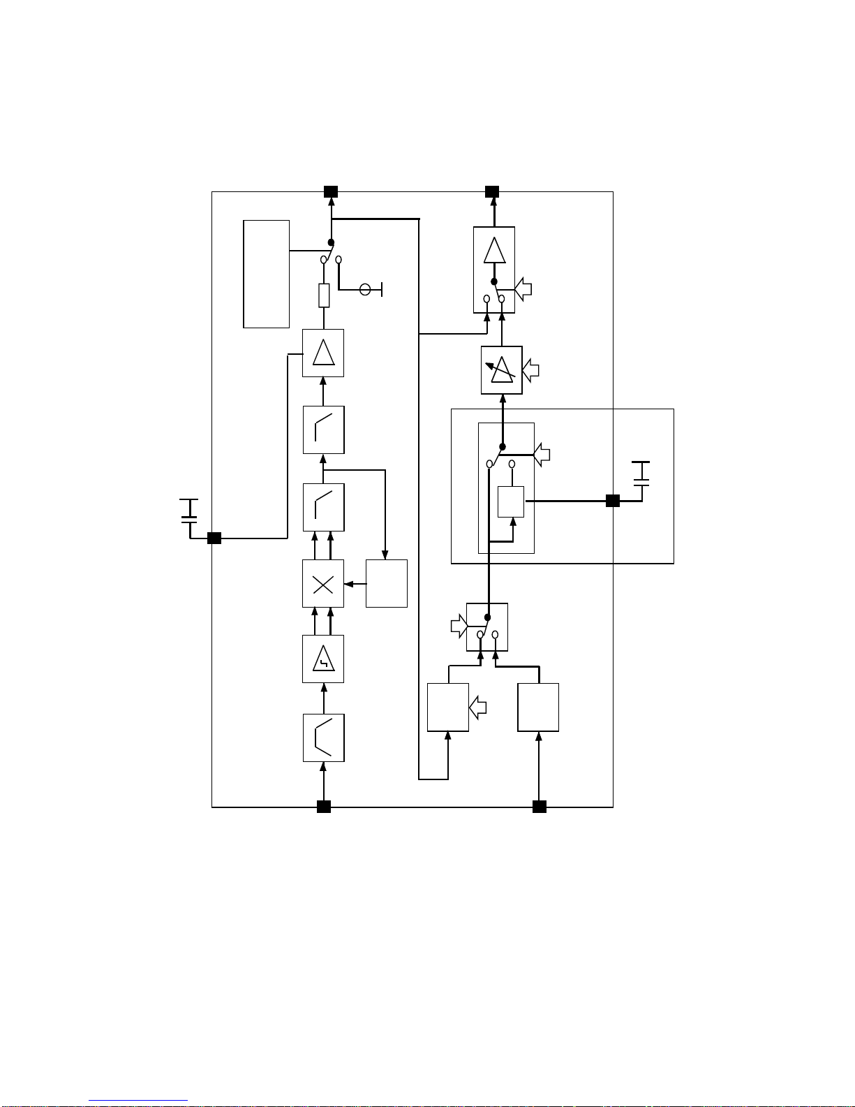
1.1.2 Vision IF
See also the related block diagram as well as the diagrams at the end of the report.
The main functions are:
* IF amplifier
* PLL-demodulator and alignment free VCO
* Video buffer
* AFC
* AGC
* Tuner AGC
* Video identification
These functions will be described next in this section.
The TDA884X includes an integrated vision-IF. This gives advantages compared to a s tand alone IC
for vision-IF only. Some advantages are:
I
2
C bus commands are available f or many control f unctions and alignment. T his saves a pins and
external components.
Optimal performance is achieved by means of timing/gating signals derived from the
synchronization part.
Build-in accuracy of circuits is derived by use of the available chroma cry stal oscillator.
3DQDVRQLF
4
* IF-amplifier
The IF-amplifier has s ymmetr ical inputs and co nsists of three AC coupled differential ga in stages wit h
AGC function. Due to the AC coupli ng, biasing is simple so that casc ades can be used and no DC
feedback is necessar y. The gain control range of the IF amplifier is 64 dB m inim al. T he inp ut sensi tivit y
for AGC onset is 70 m V typical. T he maximal IF- gain can be reduc ed with 20dB b y means of I²C bus
IFS.
* PLL-demodulator and alignment free VCO
The IF-signal is demodulated with the hel p of a PLL detector. The PLL detector is used to regenerate a
reference signal that is in ph ase to the IF-carrier s ignal. Demodulation is achieved by m ultiplying this
reference signal with the incoming IF-signal. This reference signal is a clean signal that does not
contain video information; this bandwidth (approx. 60kHz) is determined by the PLL loopfilter pin 5.
The demodulator can handle both negat ive and nega tive m odul ation, se lecti on is done with I²C bus bit
MOD.
A low pass filter after the demodulator output reduces the higher frequency demodulation products.
The voltage controlled os cillator, VCO, is ali gnment f ree and mak es the conc ept even m ore attr active.
No external coil is required any more. It saves both the coil costs and an alignment. As regards EMC
the system becomes more robust. The required IF-system frequency 38.9, 45.75MHz, including
SECAM-L’, is selected by I²C. The correct VCO frequency is determined by the calibrator system
which uses one of the actual chroma crystal as reference. Calibration occurs automatically after
power-on and every time after loss of sync lock (I
2
C bit SL)
The PLL catching range is plus/min 1MHz arou nd t he selec ted IF- frequency. W ithin this range th e P LL
ensures automatic tracking to the incoming frequency. The PLL is basically an "FPLL", Frequency
Phase Lock Loop system. T his extra fr equency detec tor gives an output s ignal to the PLL loopfilter as
long as a difference in frequency is detected. This ensures fast catching.
The PLL loopfilter time constant can be made fast vi a Fast Filter IF-PLL, FFI . This functio n has been
made available to handle RF-transmitter signals with large phase modulation (for special market
areas).
* Video buffer
The video buffer is requ ired to provide a low ohmic video output with the right amplitude and t o pr ot ec t
this output for the occur rence of noise peaks , refer to figure below. The video buffer also contains a
level shifter and gain stage for positive and ne gative modulation in order to pr ovide a correct video
amplitude and DC level.
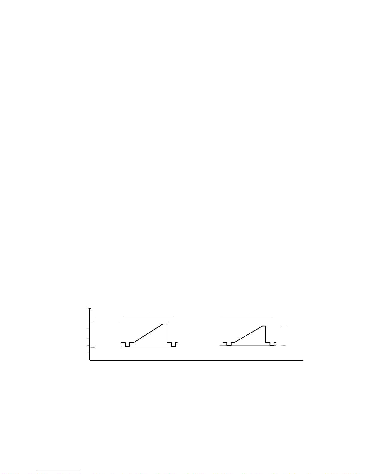
The video buffer bandwidth is typic al 9 MHz. The video output am plitude is 2.2Vpp (s ync inclusive),
independent of the supp l y voltage. A white spot clam p prevents the video am plitu de b ecom ing greater
than 5.3V typical. A noise clamp prevents the video output bec oming l ess than 1.7V typical . (Top sync
is approx. 2V) For strong signal only, the noise peak is inverted to black level.
zero level
white spot clamp
top white
zero levelnoise inv. clamptop sync.
1
2
3
4
5
Video out
[V]
Negative
Positive
Fig 1: Video signal for negative and positive modulation
The IF part can be switched-off by means of I²C bus comm and VSW. The internal CVBS input than
can be used (with minimum components) as external input, for instance for satellite.

3DQDVRQLF
5
* AGC
An AGC system controls the IF amplifier gain such that the video output amplitude is constant.
The demodulated video signal is supplied, via a low pass filter, to an AGC detector with external
decoupling capacitor. The AGC detector voltage controls directly the IF gain stages.
Negative/positive modulation:
For optimal AGC behavior the charge an d discharge current of the AGC are chosen so that both, a
relative fast AGC, as well a low tilt are poss ible for positive and neg ative modulated signa ls with the
same AGC capacitor.
A SECAM-L speed-up circuit improves the AGC settling time after IF-signal loss.
With tilt is mend the video amplitude var iation due to les s "mem ory" func tion of the AGC ca pacitor). In
Fig 2 the tilt is given during a field period for positive modulated signals. For negative modulated
signals the tilt is line frequent. For negative modulated signals the AGC is a top sync detector.
Positive modulation:
For positive modulated signa ls the AGC is a t op white AG C includin g black lev el clamp whic h mak ing
the video amplitude independent of video contents.
A top white AGC requires a 100% white r eference pulse in order to be indep endent of video co ntents.
Suitable for that purpos e is the whi te p uls e ( Video I n ser tio n Test Signal, VITS) in l ine 1 7 an d 3 30 - see
Fig 2.
Because the time constant is lar g e (AG C c urr e nt is decr eas ed f or pos it iv e modulation) the AGC will be
independent of the video contents between the reference pulses.
The maximum tilt per field is defined by the external capacitor, the AGC steepness and the small
discharge current in this mode.
//
one field
100% white
tilt
AGC voltage
Reference
pulse
Video output
signal
Fig 2: Positive modulated signal with top white reference pulse
This top white AGC h owever is not opt imal f or those sign als that have nei ther a white ref erence pu lse
or white video inform ation (e.g. with some VCR signals ). Due to the top level AGC principle a gra y
scene becomes white an d a dark scene becom es gray, see Fig 3. Th is behavior can be avoided by
means of the black level clamp.
3DQDVRQLF
6
Original video signal
with/without ref. pulse
Demodulated signal on video output
Not optimal behaviour Optimal behaviour
Ref
pulse
100%
Ref pulse 100%, luma 50%
Ref pulse, top white<100%
50%
100%
50%
a
100%
Top white AGC only
b
Ref
pulse
100%
Top white AGC
Black clamp AGC
50%
100%
50%
c
Fig 3: Top white and black clamp AGC
The Fig 3 “b” sho ws tha t the v id eo amplitude is increased by the top wh ite AGC, s uc h tha t 10 0% whit e
is obtained. As a consequence the black level increases also.
The black level clamp AG C in “c” pre vents this b ehav ior a nd beco m es autom atically act ive if the v ideo
black level on the video output increases.
In the external mode only the top white AGC is active. The black clamp AGC than is switched off
because the internal signal is not synchronized any more to the horizontal oscillator.
SECAM-L speed-up circuit:
In case of positive modulation and large reduction of the incoming IF-input le vel a speed-up c ircuit is
needed. This because the AGC action is slo w since the AGC dischar ge current is sm all (450nA), for
minimizing the tilt.
The speed-up circuit measures the amplitude of the video output signal and will react after
approximately 60ms if the video output is continuously below 80% white level.
If the speed-up is activated the AGC capacitor will be discharged with a current of 50mA.
* Tuner AGC
The tuner AGC is pro vided to reduce the tuner ga in and thus t he tuner outp ut voltage when recei ving
strong RF signals. The tuner AGC takes over when t he IF input re aches a c ertain input lev el, t hat can
be adjusted by I²C function AGC take over.
The tuner gain can be reduced by means of the open collector output pin 54.
* AFC
AFC output information is available for search tuning. With the alignment free concept this AFC
information is very accurate and deri ved via a counter. The AFC output is availa ble by the I²C bus
outputs AFA, AFB.
The AFC window width can be increased by means of I²C bus AFW. This allo ws bigger frequency
steps during search tuning.
Notice: AFC inform ation is updated once a field during the v ertical retrace and only valid when the
coincidence detector is in-lock (SL=1)
* Video identification
The IF-part includes a stand-alone video identification circuit. This makes the ident function
independent of the s ync part. The ident output is availabl e by I²C bus, IFI, and can be used d uring
search tuning and for automatic sound mute in full scart application.
The video ident circuit measures the main frequency of the input signal, which should be
approximately 16kHz.The video ident. can be connected to the "internal" video signal or to the
selected CVBS input signal.
3DQDVRQLF
7
IF
A
m
plifier
V
C
O
PL
L
FFl FastFilterIF
T
uner
take over
adjust
M
O
D
G
ating
A
G
C
detector
L
PF
L
PF
D
em
odulator
C
alibrator
A
FC
IFA
, IFB
, IFC
IF frequency selection
A
FW
A
FA
A
FB
f
sc
M
O
D
pos. / N
eg.
V
SW
V
ideo m
ute
V
ideo
Ident
IF1
PL
L
loopfilter
A
G
C
decoupling
N
.C
.
IF input 1
IF input 2
T
uner A
G
C
out
IF V
ideo out
4
3
48
49
54
53
6
5
Fig 4 : Block diagram: Vision IF

3DQDVRQLF
8
1.1.3 Sound
See also the related block diagram as well as the diagrams at the end of the report.
The main functions are:
* Limiter
* PLL-Demodulator
* Pre-amplifier and mute
* Audio switch
* Volume controlled amplifier
These functions will be described next.
* Limiter
The sound carrier signal is supplied to this lim iter input via an external bandpass filter. This external
bandpass filter is used for selectivity, the internal f ilter at th e p in is us ed f or no ise r ed uc ti on. The limiter
consists of AC couple d amplifier stages. T he minimum input amplitude for limiting is typical 1m Vrms.
The input impedance is 8K5 in parallel with 5pF.
* PLL-Demodulator
Sound demodulation is achieved by a PLL FM-demodulator and does not need any external
alignment.
The PLL has been optimized for a low S/N ratio with still an acceptable po wer consumption. T he PLL
catching range is 4.2 - 6.8MHz, which is suitable for all multistandard applications.
* Pre-amplifier and mute
The pre-amplifier outp ut sign a l a va ilabl e at the deemphasis pin can be used for SCA RT applic at ion. At
this pin the deemphas is capaci tor has to b e connec ted. T he output le vel is 500mVrms for a FM swing
of 50kHz.
A pre-amplifier with DC feedback has been provided . The DC com ponent of the deemphasis s ignal is
always 3V, also during sound mute. Sound mute plop is therefore minimized.
When no video signal is identified the deemphasis output is automatically muted.
* Audio switch
An audio switch has been provide d for full SCART function. T he audio switc h is controll ed by the I2C
bus Source Select INA /INC. For positive modulati on, MOD, the ext ernal sound inp ut is automatical ly
selected for an external AM sound demodulator.
* Volume controlled amplifier
The volume control is active for both internal and external audio signals. The nominal gain is +9dB and
minimal -71dB, which gives a total control range of 80dB minimal.
3DQDVRQLF
9
L
im
iter
Sound decoupling
A
V
L
decoupling
E
xt. audio in
1
2
45
56
15
55
A
V
L
-6dB
0 / -6dB
L
PF
B
PF
PL
L
dem
odulator
L
oopfilter
Pre-am
plifier
A
udio
sw
itch
A
V
L
V
olum
e
FA
V
Fixed audio
IN
A
, IN
B
IN
C
, M
O
D
X
A
= 0: 0dB
X
A
= 1: -6dB
V
C
O
A
utom
atic volum
e level
V
olum
e control
1 - 10M
H
z
15k
3V
+15dB
-71dB
500m
V
rm
s
m
ax. 2V
rm
s
500m
V
rm
s @
50kH
z sw
ep
250m
V
rm
s @
25kH
z sw
eep
A
V
L
feature not
on all m
odels
Sound m
ute:
IN
T
m
ode via: SL
= 0, SM
= 1
E
X
T
m
ode via: IFl = 0, SM
= 1
ST
B
= 0 ; SM
= 1
N
o m
ute ; V
IM
= 1
Sound IF in
D
eem
phasis /
A
udio line-out
A
udio out
Fig 5: Block diagram: Sound

3DQDVRQLF
10
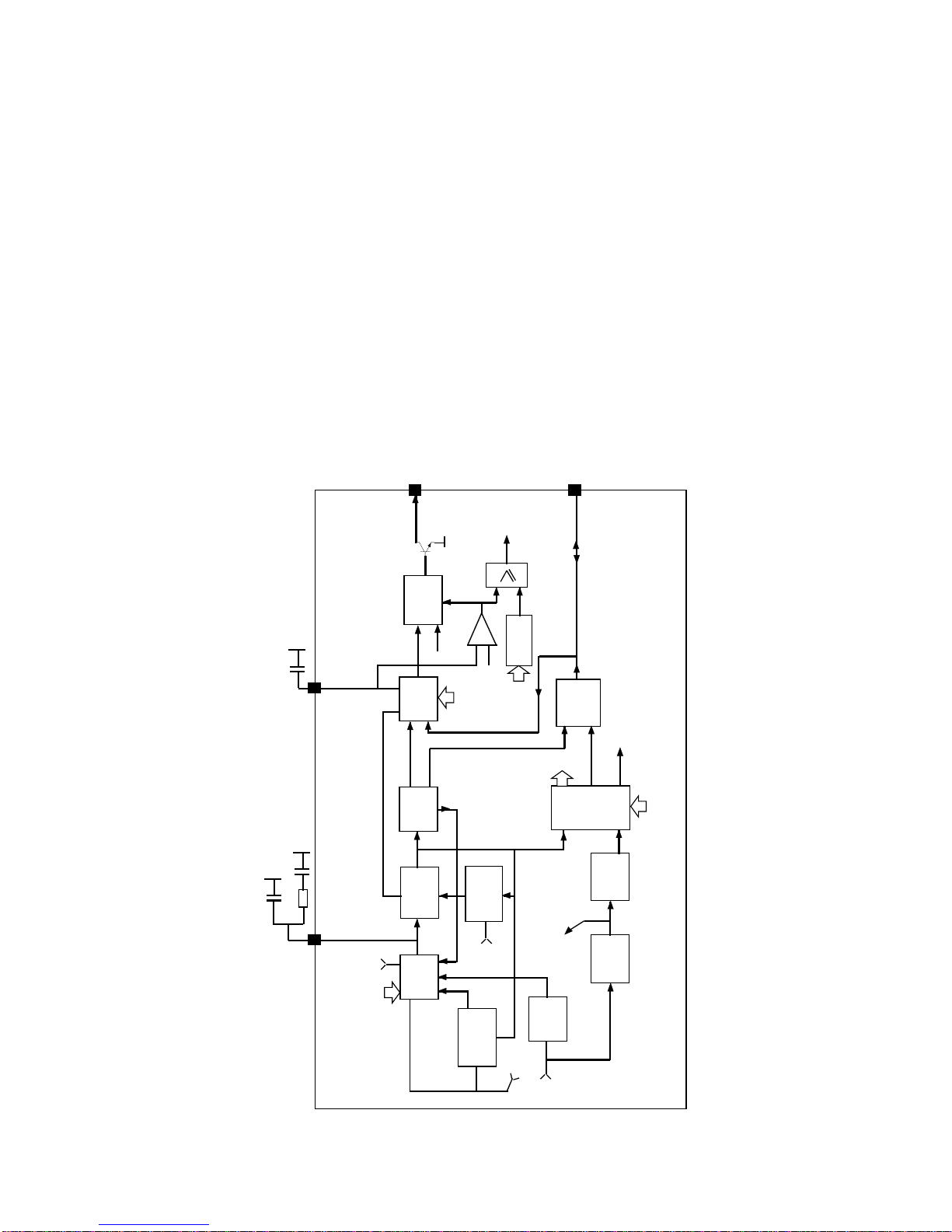
1.1.4 Horizontal and vertical synchronization
See also the related block diagram as well as the diagrams at the end of the report.
The main functions are:
* Horizontal sync separator
* Horizontal oscillator and calibration system
* PHI-1 detector
* PHI-2 detector and sandcastle generation
* Horizontal output with slow start/stop facility
* Coincidence detector
* Noise detector
* Vertical sync separator
* Vertical divider system
* Horizontal sync separator
The horizontal sync separator is supplied from the CVBS/Y inputs (chosen video source). For
horizontal synchronization the s ync separator slices in the middle of the s ync pulse a nd the slicing
level is independe nt of the sync pulse amplitude. For t he vertical synchroni zation the sync pulse i s
sliced at a level of about 30% (closer to the b lack level). This ensures optim al output signals for a
stable horizontal and vertical deflection under various video input conditions.
The top sync level is clamped at the CVBS input. The black level is stored internally.
* Horizontal oscillator and calibration system
The horizontal oscillator requires no external components and is fully integr ated. The adjustment for
nominal frequency is derived automatically by a calibration circuit.
The oscillator generates a sawtooth signal with double hor izontal frequency. This sawtooth signal is
used to derive several other gating and timing signals. After calibration the horizontal oscillator is
controlled by the PHI-1 loop for synchronization with the incoming video input signal.
The calibrator is res ponsible for th e autom atic adjustm ent of the horizontal osc illator. One of the color
crystals is being used as reference. For that reason a correct crystal selection by XA,XB (Xtal
selection) is ver y important during power- on. Calibration occurs durin g the vert ical retrace period and
only under following conditions:
- At power-on/ initialization
- After power dip (shutdown detection), re-initialization is required.
- After loss of synchronization (e.g. after channel switching)
* PHI-1 detector
The PHI-1 detector is a PLL circuit that synchro nizes the horizontal oscillator with the incom ing video
signal. The PLL compares the output of th e H-sync separator with the horizontal osc illator. The PLL
output current is converted to a vo ltage by means of the ex ternal loop filter. This voltage contr ols the
horizontal oscillator. The loop filter is connected externally so the time constant can be defined
according to the customer requirements. Because the static loop gain is very high there will be no
phase shift when switching between input signals with different line.
* PHI-2 detector and sandcastle
As described, the Horizontal PL L (PHI-1 loop) synchronizes the hor izontal oscilla tor with the incoming
video signal. The PHI-2 loop provides a stable picture position on screen.
This is necessar y because d ue to b eam cur rent vari ations t he stor age t im e of the lin e tr ansistor vari es
and, due to that, the picture position on screen.
The PHI-2 detector compares the horizontal oscillator signal (reference) with the horizontal flyback
input pulse, pin 41. This flyback pulse is related to the horizontal deflection.
The PHI-2 circuit shifts the horizontal drive, pin 40, such that the picture position on screen is constant.
The flyback input pin 41 is combined with the sandcast le output. This combined func tion provides a
three level sandcastle signa l and is available starting with the highes t level: burstk ey, line blan king (=
flyback pulse) and vertical blanking.
The phase of the video s ignal with respect to the deflection current can be adapted by I²C bus HS
(horizontal shift, shift picture left/right).
The PHI-2 loop filter is a first order filter. The capacitor is connected externally on pin 42.

3DQDVRQLF
11
* H-output and slow start/stop
The horizontal output is the driver pin for the line deflection. It is an open collector output. Under
normal operation condition the duty cycle of the output pulse is 45% off ( Hout = hi g h) / 5 5% o n (H o ut =
low).
A build in slow start/stop circuit ensures a smooth start/stop behavior of the line deflection and protects
the line output transistor.
During switch-on the horizontal outp ut starts with the double frequency (31.25 k Hz) and with a duty
cycle of 75% off (Hout = high)/ 25% on (Ho ut = l o w). After abou t 50ms the frequency is changed to the
normal value (15.625 kHz) and the duty cycle to 45% off (Hout = high) / 55% on (Hout = low).
Also during switching-off via stand by (STB) the frequenc y is switched t o the double value and the
RGB drive is set to maximum to dischar ge the voltage on the EHT capacitor to h alf of its maximum
value. After about 100ms the RGB drive is set to minimum and 50ms later the horizontal drive is
switched-off.
* Noise detector
The TDA8844 has an internal noise detector which is used to switch the time constant of the horizontal
PLL.
The input of the detector is connected to the selected CVBS input.
The noise detector measures the RMS value of the noise during a part of the sync pulse. (The
detection level is 100mVrms and corresponds to 20dB S/N-ratio for 1Vpp CVBS).
A field counter is used for hysteresis and decides after 2 successive fields whether noise is detected.
When noise is detected the horizontal PLL time constant is switched to slow.
* Coincidence detector
The coincidence detector detects whether the incoming CVBS signal is synchronized with the
horizontal oscillator, thus whether the PHI-1 loop is in-lo ck . The out put is availa ble b y I²C bus , SL, a nd
can be used for search tuning and OSD. For out of lock condition the c oincidence detector can be
made less sensitive (about 5 dB) by control bit STM (search tuning mode). This prevents false stops.
* Vertical sync separator
The vertical sync separator separates the vertical sync pulse from the composite sync signal. This
separated sync pulse is us ed to trigger the vertica l divider s ystem. To generate a trigger p ulse for the
divider the minimum pulse width of the incoming vertical sync pulse must be 17µs.
The integrator network is designed such that for anticopy signals (e.g. Macrovision) with vertical
pulses of 10µs (on) and 22µs (off) still a vertical s ync pulse is generated. ( Because more lines with
vertical pulses are prese nt, pulse width of less than 17 µs is allowed, by integratio n still the required
level is reached).
* Vertical divider system
The divider system uses a counter that delivers the timing for the vertical ramp generator in the
geometry processor. The clock is derived from the horizontal line oscillator.
The divider system synchronizes on the vertical sync pulse of the vertical sync separator.
The divider has three modes of operation:
1. Search mode (large window)
This mode is activated when the circuit is not synchronized or when a non-standard signal is received.
In the search mode the divider can catch between about 45 and 64.5Hz.
2. Standard mode (narrow window)
This mode is switc hed on (coming from sear ch mode) when more than 15 suc cessive vertical s ync
pulses are detected in the narrow window. When the circuit is in the standard mode and a vertical sync
pulse is missing the re trace of the vertical ram p generator is started at the end of the window (thus
automatic insertion of m issing vertical sync pu lses). As cons equence the d isturbance of the picture is
very small. The circuit will switch bac k to the search window when 6 suc ceeding vertical periods no
sync pulses are found within the window. (See also NCIN below)
In the narrow window mode the PHI-1 is inhibited during the vertical egalization pulses to prevent
disturbance.
3DQDVRQLF
12
3. Standard TV-norm: divider ratio 525 (60Hz) or 625 (50Hz)
When the system is switched to the narrow window (standard mode) it is checked whether the
incoming vertical sync pulses are accord ing to the TV norm, if so IVW=1. W hen 15 standar d TV-nor ms
are counted the divider system is switche d to the standard d ivider rati o mode. In t his mode the divider
is always reset at the standard value even if the vertical sync pulse is missing.
The system switches back to the narrow windo w when 3 vertical s ync pulses are mis sed. When also
in the narrow windo w 3 vertical sync pulses are missed, the divider will switch to the s earch window
mode.
As described above the vertic al divider needs some wait ing time before s witching back to the search
window mode. When a f ast reaction is req uired for instance dur ing channel swit ching the s ystem can
be forced to the search window by means of I²C bus, setting NCIN = 1 (vertical divider mode).
Immediate after forcing to search mode NCIN has to be set back to 0 for optimum performance.
The vertical synchronization mode of operation can be selected by I²C bus FORF/S, forced field
frequency.
Furthermore, 50/60Hz identification is available by I²C bus FSI (50/60Hz), and norm signal
identification with IVW. Interlace can be switched on and off by I²C bus DL.
PH
l1 Filter
42
41
40
T
im
ing
PH
l1
H
out
C
alibration
H
orizontal
Flyback in /
detector
H
orizontal
oscillator
PH
l2
detector
Slow
start
&
Stop
system
V
ertical
D
ivider
Sandcastle
G
enerator
V
sync.
separation
separation
H
sync.
N
oise
detector
C
oincidence
detector
B
lanking
G
enerator
slow
start
&
stop
+
-
6V
H
B
L
, L
B
M
H
O
B
IV
W
F
S
I
H
S
H
F
O
R
F
, F
O
R
S
N
C
IN
, D
L
H
sync
H
sync
F
sc
L
um
a
from
F
ilters &
S
w
itches
V
ertical pulse
for geom
etry
Sandcastle out
D
rive
PH
l2 Filter
V
ID
P
O
C
F
O
A
F
O
B
IF
1
43
R
G
B
blank 1
Fig 6 : Block diagram: Horizontal and vertical synchronization
3DQDVRQLF
13
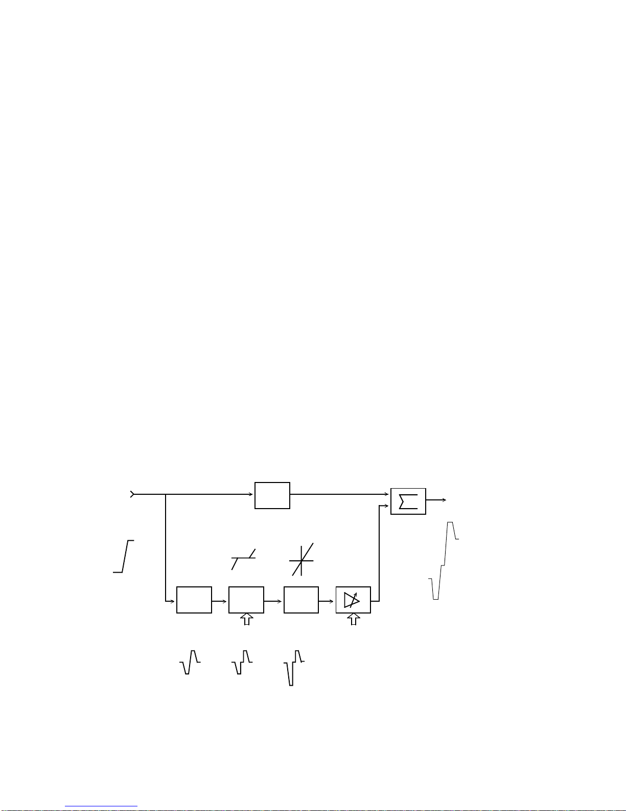
1.1.5 Luminance and chrominance signal processing
* Chrominance signal processing
For chroma signal processing, the select ed si gna l is sup plied to both the PAL/NTSC chr oma bandpass
filter and the SECAM cloche filter vi a a variable gain amplifier whic h is controlled by ACC and ACL
detection circuits.
The dynamic range of the ACC is 26dB and de tects only the burst am plitude; consequent ly the burst
signal at the bandpass/cloc h e f ilt er in put is cons tan t f or a burs t s i gna l ran ge +6dB -> -20dB where 0dB
= 300m
VPP burst.
The ACL is a chroma amplitude detector and is active when the chroma/burst ratio exceeds
approximately 3. It ens ures that CVBS signal to chrom a bandpass & cloche filter is limited for large
chroma/burst ratios (>3). which results in a constant saturation for such non-standard transmissions.
The ACL is independent of the ACC; it con trols onl y the chrom a am plitude and do es no t influenc e the
color burst sensitivity. The ACL function can be switched on/off via bus command ACL.
The output signal of the chr om a bandpass circ uit is s uppli ed to th e PAL/NTSC decoder and the o utpu t
signal of the cloche filter is supplied to the SECAM decoder for further chroma processing.
* Luminance signal processing
For luminance processing, the selected video signal is supplied to the H/Vsync circuits for sync
processing and also to an adjustable delay line (0ns - 320ns, minimum step is 40ns, controlled via b us
bits YD0-YD3). The chroma trap is bypassed for no burst transmissions when in own intelligence
mode (automode). In Y/C modes the video signal follows a direct path with 160ns delay so as to
ensure similarity with chroma path delay. The output signal is supplied to the peaking and coring
stages whose operation is illustra ted be lo w.
The peaking function is realized with τ= 160ns delay cells (i.e. frequency response reaches a
maximum at a frequency f = 1/2τ= 3. 12 5MH z) .
The coring function has a non-linear transfer characteristic which implies that a noise suppression
range (coring range) of 15 IRE is realized. This means that extra n oise introduced du e to increased
gain of the peaking amplif ier is defeated by the c oring function. The cor ing stage is activated via the
I²C bus (COR).
Asymmetric peak ing is introduced to e nhance picture definition. The negat ive/positive overshoot rat io
is approximately 1.8. The degree of peaking is controlled by the peaking amplifier via the I²C bus
(PEAKING). The output of the peaking amplifier is s ummed with the delayed (1 60ns) selected video
signal (see Fig 7).
The output of the peaking/coring stages (i.e. o utput of summing stage) is fed as internal luminance
signal (Y
INT
) to the YUV selection circuit (see YUV/RGB processing part).
SUMMING
STAGE
25IRE
100IRE
45IRE
Nominal PEAKING
PEAK
ASSYMETRIC
PEAKING
CORING
FUNCTION
COR
PEAKING
FUNCTION
15IRE
100IRE
(b1/wh)
Selected
VIDEO
Signal
DELAY
160ns
25IRE
45IRE
50IRE50IRE
Fig 7: Peaking and coring operation

3DQDVRQLF
14
C
S1, C
S0
38
C
V
B
S &
Y
/C
select
output
select
Peaking
&
C
oring
burst
detect
chrom
a
detect
C
V
B
S B
uffer
IN
A
, IN
B
, IN
C
0 - 320nS
160nS
C
V
B
S
Y
/ C
C
hrom
a trap
no burst in auto m
ode
IN
A
, IN
B
IN
C
T
o Sync.
L
um
a
C
hrom
a
A
C
C
A
C
L
C
loche
C
hrom
a (SE
C
A
M
)
F
sc
Filter T
uning
C
hrom
a (PA
L
/ N
T
SC
)
C
O
R
Peaking
C
B
A
C
L
Y
D
0 - Y
D
3
(26)
11
10
13
17
C
V
B
S1
out
C
hrom
a
C
V
B
S2
out
C
V
B
S / Y
C
V
B
S int.
C
V
B
S ext.
Fig 8 : Block diagram: Filters and CVBS/Y/C switches

3DQDVRQLF
15
1.1.6 Color Decoder
See also the related block diagram as well as the diagrams at the end of the report.
The main functions are:
* PLL/VCXO
* PAL/NTSC identification
* SECAM identification
* ASM ( Automatic System Manager )
* (R-Y)/(B-Y) demodulation
* PLL/VCXO
The PLL operates during the burstkey period; it generates a VCXO reference signal ( f
VCXO
), in
phaselock with the inc oming burst s ignal ( f
BURST
). Prior to lock condit ion, the signals f
VCXO
and f
BURST
are not synchronous and are present at phase detector input. The loop filter averages the phase
detector output current and the resulting control signal to the VCX O is proportional to Sin(2π∆ft) where
∆f = f
VCXO
- f
BURST
.
A lock situation occurs when ∆f < VCXO ho ld ing r ang e; once in lock, the phase detector output c ur rent
is proportional to θ
E
= θ
VCXO
- θ
BURST
(θE is the static phase error).
The combined phase detector and VCXO sensitivity is high to ensure a small static phase error.
For fast color acquisition, the phase detector is in high gain mode when a color system is not yet
identified.
The VCXO loop (not to be confused with phase lock ed loop, PLL) compensates f or any attenuation
loss or phase shift in th e crystal so that the it’s loop gain is u nity and loop phase shift is zero. The
VCXO reference outputs (0° and 90°) are stable sinusoids.
VCXO oscillation is at s eries resonance of the selected X tal. Since the PLL automatically tunes th e
VCXO to the burst (if inside the PLL holding range) fine tuning of the VCXO with a trimming
capacitance is not necessary.
The motional capacitance of the Xtal is dam ped by the inter nal resistance of the VCXO pins (i.e. 1K )
in order to realize the holding range.
The catching range ( pull-in) of the PLL loop is gover ned by the PLL loop filter; the loop filter can be
chosen so that PLL holding and catching range are similar (direct catching).
The HUE phase rotator is inoperational when the PLL is active (i.e. no phase rotation during the
burstkey period). Outside the burstkey period, the hue control rotates the VCXO reference phases
from -40° to 40° linearly for I²C bus command (HUE: 0 --> 63), see also device specification.
* PAL/NTSC demodulation
The 0° and 90° reference signa ls from the VCXO are s upplied to the HUE phas e rotator; it's outputs
(H0, H90) are supplied to the (B-Y) and (R-Y) burst demodulators respectively.
The demodulated bur st from the (B-Y) dem odulator supp lies NT SC ident i nformation to the ASM (IDN
signal). The demodul ated burst from (R-Y) demodulator suppli es PAL ident inform ation to the ASM
(IDP signal). For correct dem odulation of (R-Y) PAL burst and chrom a signals, then the H90 sig nal
requires 180° phase shift on alternate lines. This is realized with the H/2 switch before the (R-Y)
demodulator. It is not active during demodulation of NTSC signals.
The (B-Y)/(R-Y) baseband signals are obtained from the chroma signal by the (B-Y)/(R-Y)
demodulators, filtered and supp lied via the PAL /SECAM switch (PS) to the internal bas eband delay
line.
The demodulator gain ratio (B-Y)/(R-Y) is typically 1.78 in order to compensate for scaling in the
transmitter. For NTSC applications it is poss ible to bypass the dela y line via I2C bus c ommand BPS;
the gain is also corrected then by a factor two. The V
INT
and U
INT
signals from dela y line outputs are fed
to the YUV selection circuit (see YUV/RGB processing part).
* SECAM demodulation
SECAM demodulation is realized with a PLL type demodulator.
When the VCXO is connected t o pin 35 (controlled by XTS) and if a 4 .43MHz Xtal is prese nt on that
pin then SECAM demodulation is possible. The auto tun ing loop, consisting of PLL demodulator and
oscillator, ensures that the PLL osci llator is locked to the 4.43MH z Xtal frequency during calibration
time in the vertical r etrace period. T he SECAM r eference v oltage, generated at pin 16, is regulated in
order that the PLL demodulator ou tput is set to a reference voltage deri ved from a stable bandg ap
voltage.
Outside calibration the oscillator remains tracking the SECAM chrominance resulting in the
corresponding demodulated voltage. This is delivered to the LF de-emphasis stage and to the line
 Loading...