

Panasonic TX-LR19X10 Service manual
ORDER NO. MTV0901812CE
Model No. TX-LR19X10
Chassis: KM02
Destination: CIS
LCD TV
Specifications
Power Source AC SINGLE 220 - 240 V, 50/60 Hz
Power Consumption
Average use 39 W
Standby condition 0.9 W
Display panel
Aspect Ratio 16:9
Visible screen size 47 cm (diagonal)
409.8 mm (W) × 230.4 mm (H)
Number of pixels 1,049,088 (1,366 (W) × 768 (H))
Sound
Speaker Full range × 2 pcs, 8 Ω
Audio Output 6 W (3 W + 3 W), 10% THD
Headphones M3 (3.5 mm) stereo mini Jack × 1
PC Signals VGA, SVGA, XGA
SXGA ...... (compressed)
Horizontal scanning frequency 31 - 69 kHz
Vertical scanning frequency 59 - 86 Hz
Receiving Systems / Band name SYSTEMS FUNCTIONS
1 PAL B, G, H
2 PAL I
3 PAL D, K
4 SECAM B, G
5 SECAM D, K
6 SECAM K1
7 NTSC M (NTSC 3.58 / 4.5MHZ)
Reception of broadcast transmission and
playback from video cassette tape recorders.
© Panasonic Corporation 2009. Unauthorized
copying and distribution is a violation of law

TX-LR19X10
8 NTSC 4.43 / 5.5 MHz
9 NTSC 4.43 / 6.0 MHz
10 NTSC 4.43 / 6.5 MHz
11 NTSC 3.58 / 5.5 MHz
12 NTSC 3.58 / 6.0 MHz
13 NTSC 3.58 / 6.5 MHz
14 SECAM I
15 PAL 60 Hz / 5.5 MHz Playback from Special Disc Players and
16 PAL 60 Hz / 6.0 MHz
17 PAL 60 Hz / 6.5 MHz
Receiving Channels (Analogue TV)
VHF BAND 2 - 12 (PAL / SECAM B, K1)
0 - 12 (PAL B AUST.)
1 - 9 (PAL B N.Z.)
1 - 12 (PAL / SECAM D)
1 - 12 (NTSC M JAPAN)
2 - 13 (NTSC M USA)
UHF BAND 21 - 69 (PAL G, H, I / SECAM G, K, K1)
28 - 69 (PAL B AUST.)
13 - 57 (PAL D, K)
13 - 62 (NTSC M JAPAN)
14 - 69 (NTSC M USA)
CATV S1 - S20 (OSCAR)
1 - 125 (USA CATV)
C13 - C49 (JAPAN)
S21 - S41 (HYPER)
Z1 - Z37 (CHINA)
5A, 9A (AUST.)
Aerial - Rear VHF / UHF
Operating Conditions Temperature : 0°C - 35°C
Humidity : 20 % - 80 % RH (non-condensing)
Connection Terminals
AV1 Input AUDIO L-R RCA PIN Type × 2 0.5 V [rms]
VIDEO RCA PIN Type × 1 1.0 V [p-p] (75 Ω)
AV2 Input AUDIO L-R RCA PIN Type × 2 0.5 V [rms]
VIDEO RCA PIN Type × 1 1.0 V [p-p] (75 Ω)
COMPONENT Y 1.0 V [p-p] (including synchronization)
, PR/C
P
B/CB
R
Others HDMI 1 / 2 Input TYPE A Connectors • This TV supports “HDAVI Control 4” function.
PC Input HIGH-DENSITY D-SUB 15 PIN R, G, B / 0.7 V [p-p] (75 Ω)
Card Slot SD Card slot × 1
Monitor
Output
AUDIO L-R RCA PIN Type × 2 0.5 V [rms] (High impedance)
VIDEO RCA PIN Type × 1 1.0 V [p-p] (75 Ω)
Dimensions (W x H x D) 472 mm × 361 mm × 174 mm (With Pedestal)
472 mm × 323 mm × 67 mm (TV only)
Mass 5.5 kg Net (With Pedestal)
5.0 kg Net (TV only)
Design and specifications are subject to change without notice. Weight and dimensions shown are approximate.
Playback from special VCR’s or DVD.
Special VCR’s or DVD.
± 0.35 V [p-p]
HD, VD / TTL LEVEL 2.0-5.0 V [p-p] (high impedance)
2

TABLE OF CONTENTS
PAGE PAGE
1 Safety Precautions-----------------------------------------------5
1.1. General Guidelines---------------------------------------- 5
1.2. Touch-Current Check------------------------------------- 5
1.3. KM02 Chasis Block Diagram--------------------------- 6
2 Prevention of Electro Static Discharge (ESD) to
Electrostatically Sensitive (ES) Devices------------------7
3 About Lead Free Solder (PbF) ------------------------------- 8
4 Power LED Blinking Timing----------------------------------- 9
5 Location of Controls and Components ------------------10
5.1. Wire Dressing ---------------------------------------------10
6 Disassembly and Assembly Instructions---------------11
6.1. AC Cord Dressing----------------------------------------11
6.2. AC Cord Installation--------------------------------------12
6.3. LED Panel Installation And Fitting--------------------14
6.4. Control Panel Assembly --------------------------------15
6.5. Control Panel Assembly and VESA Metal
Installation--------------------------------------------------16
6.6. Side AV Bracket Assembly-----------------------------17
6.7. Speaker Installation--------------------------------------18
6.8. EMI Spec (LVDS)-----------------------------------------19
6.9. Chassis and Frame Screw Position------------------20
6.10. Chassis Frame Fix to LCD Panel---------------------21
6.11. Fix Chassis Frame and Cont. Panel Bracket------22
6.12. Power Button, Top VESA Metal and Cont.
Panel Assembly-------------------------------------------23
6.13. VESA (BC) Installation----------------------------------24
6.14. Pedestal Assembly---------------------------------------26
7 Service Mode Adjustment ------------------------------------27
7.1. Self Check Mode -----------------------------------------27
7.2. Hotel Mode Adjustment---------------------------------27
7.3. Hotel Mode-------------------------------------------------27
8 Measurements and Adjustments---------------------------28
8.1. Voltage Check---------------------------------------------28
8.2. Power Supply for Writing Data in Board
Indivisual.---------------------------------------------------28
8.3. White Balance---------------------------------------------28
9 Printed Circuit Board-------------------------------------------29
9.1. A-Board -----------------------------------------------------29
9.2. A-Board -----------------------------------------------------30
10 Schematic Diagram---------------------------------------------31
10.1. Schematic Diagram Notes -----------------------------31
10.2. A Board -----------------------------------------------------32
10.2.1. A Board - Sheet : 001 (1 / 8)----------------------32
10.2.2. A Board - Sheet : 001 (2 / 8)----------------------33
10.2.3. A Board - Sheet : 001 (3 / 8)----------------------34
10.2.4. A Board - Sheet : 001 (4 / 8)----------------------35
10.2.5. A Board - Sheet : 001 (5 / 8)----------------------36
10.2.6. A Board - Sheet : 001 (6 / 8)----------------------37
10.2.7. A Board - Sheet : 001 (7 / 8)----------------------38
10.2.8. A Board - Sheet : 001 (8 / 8)----------------------39
10.2.9. A Board - Sheet : 002 (1 / 6)----------------------40
10.2.10. A Board - Sheet : 002 (2 / 6)----------------------41
10.2.11. A Board - Sheet : 002 (3 / 6)----------------------42
10.2.12. A Board - Sheet : 002 (4 / 6)----------------------43
10.2.13. A Board - Sheet : 002 (5 / 6)----------------------44
10.2.14. A Board - Sheet : 002 (6 / 6)----------------------45
10.2.15. A Board - Sheet : 003 (1 / 2)----------------------46
10.2.16. A Board - Sheet : 003 (2 / 2)----------------------47
TX-LR19X10
10.2.17. A Board - Sheet : 004 (1 / 5) --------------------- 48
10.2.18. A Board - Sheet : 004 (2 / 5) --------------------- 49
10.2.19. A Board - Sheet : 004 (3 / 5) --------------------- 50
10.2.20. A Board - Sheet : 004 (4 / 5) --------------------- 51
10.2.21. A Board - Sheet : 004 (5 / 5) --------------------- 52
10.2.22. A Board - Sheet : 005 (1 / 4) --------------------- 53
10.2.23. A Board - Sheet : 005 (2 / 4) --------------------- 54
10.2.24. A Board - Sheet : 005 (3 / 4) --------------------- 55
10.2.25. A Board - Sheet : 005 (4 / 4) --------------------- 56
10.2.26. A Board - Sheet : 006 (1 / 9) --------------------- 57
10.2.27. A Board - Sheet : 006 (2 / 9) --------------------- 58
10.2.28. A Board - Sheet : 006 (3 / 9) --------------------- 59
10.2.29. A Board - Sheet : 006 (4 / 9) --------------------- 60
10.2.30. A Board - Sheet : 006 (5 / 9) --------------------- 61
10.2.31. A Board - Sheet : 006 (6 / 9) --------------------- 62
10.2.32. A Board - Sheet : 006 (7 / 9) --------------------- 63
10.2.33. A Board - Sheet : 006 (8 / 9) --------------------- 64
10.2.34. A Board - Sheet : 006 (9 / 9) --------------------- 65
10.2.35. A Board - Sheet : 007 (1 / 4) --------------------- 66
10.2.36. A Board - Sheet : 007 (2 / 4) --------------------- 67
10.2.37. A Board - Sheet : 007 (3 / 4) --------------------- 68
10.2.38. A Board - Sheet : 007 (4 / 4) --------------------- 69
10.2.39. A Board - Sheet : 008 (1 / 2) --------------------- 70
10.2.40. A Board - Sheet : 008 (2 / 2) --------------------- 71
10.2.41. A Board - Sheet : 009 (1 / 5) --------------------- 72
10.2.42. A Board - Sheet : 009 (2 / 5) --------------------- 73
10.2.43. A Board - Sheet : 009 (3 / 5) --------------------- 74
10.2.44. A Board - Sheet : 009 (4 / 5) --------------------- 75
10.2.45. A Board - Sheet : 009 (5 / 5) --------------------- 76
10.2.46. A Board - Sheet : 010 (1 / 2) --------------------- 77
10.2.47. A Board - Sheet : 010 (2 / 2) --------------------- 78
10.2.48. A Board - Sheet : 011 (1 / 2)----------------------79
10.2.49. A Board - Sheet : 011 (2 / 2)----------------------80
10.2.50. A Board - Sheet : 012 (1 / 5) --------------------- 81
10.2.51. A Board - Sheet : 012 (2 / 5) --------------------- 82
10.2.52. A Board - Sheet : 012 (3 / 5) --------------------- 83
10.2.53. A Board - Sheet : 012 (4 / 5) --------------------- 84
10.2.54. A Board - Sheet : 012 (5 / 5) --------------------- 85
10.2.55. A Board - Sheet : 013 (1 / 4) --------------------- 86
10.2.56. A Board - Sheet : 013 (2 / 4) --------------------- 87
10.2.57. A Board - Sheet : 013 (3 / 4) --------------------- 88
10.2.58. A Board - Sheet : 013 (4 / 4) --------------------- 89
10.2.59. A Board - Sheet : 014 (1 / 5) --------------------- 90
10.2.60. A Board - Sheet : 014 (2 / 5) --------------------- 91
10.2.61. A Board - Sheet : 014 (3 / 5) --------------------- 92
10.2.62. A Board - Sheet : 014 (4 / 5) --------------------- 93
10.2.63. A Board - Sheet : 014 (5 / 5) --------------------- 94
10.2.64. A Board - Sheet : 015 (1 / 2) --------------------- 95
10.2.65. A Board - Sheet : 015 (2 / 2) --------------------- 96
10.3. P Board-----------------------------------------------------97
10.3.1. P Board (1 / 6) --------------------------------------- 97
10.3.2. P Board (2 / 6) --------------------------------------- 98
10.3.3. P Board (3 / 6) --------------------------------------- 99
10.3.4. P Board (4 / 6) ------------------------------------- 100
10.3.5. P Board (5 / 6) ------------------------------------- 101
10.3.6. P Board (6 / 6) ------------------------------------- 102
10.4. V Board--------------------------------------------------- 103
10.4.1. V Board (1 / 4) ------------------------------------- 103
3

TX-LR19X10
10.4.2. V Board (2 / 4)-------------------------------------- 104
10.4.3. V Board (3 / 4)-------------------------------------- 105
10.4.4. V Board (4 / 4)-------------------------------------- 106
11 Exploded View and Replacement Parts List --------- 107
11.1. Exploded View and Mechanical Replacement
Parts List ------------------------------------------------- 107
1 1 .2. Electrical Replacement Parts List------------------ 107
1 1.2.1. Replacement Parts List Notes ----------------- 107
11.2.2. Electrical Replacement Parts List ------------- 108
4
TX-LR19X10
1 Safety Precautions
1.1. General Guidelines
1. When servicing, observe the original lead dress. If a short circuit is found, replace all parts which have been overheated or
damaged by the short circuit.
2. After servicing, see to it that all the protective devices such as insulation barri ers, insulation papers shields are properly
installed.
3. After servicing, make the following leakage current checks to prevent the customer from being exposed to shock hazards.
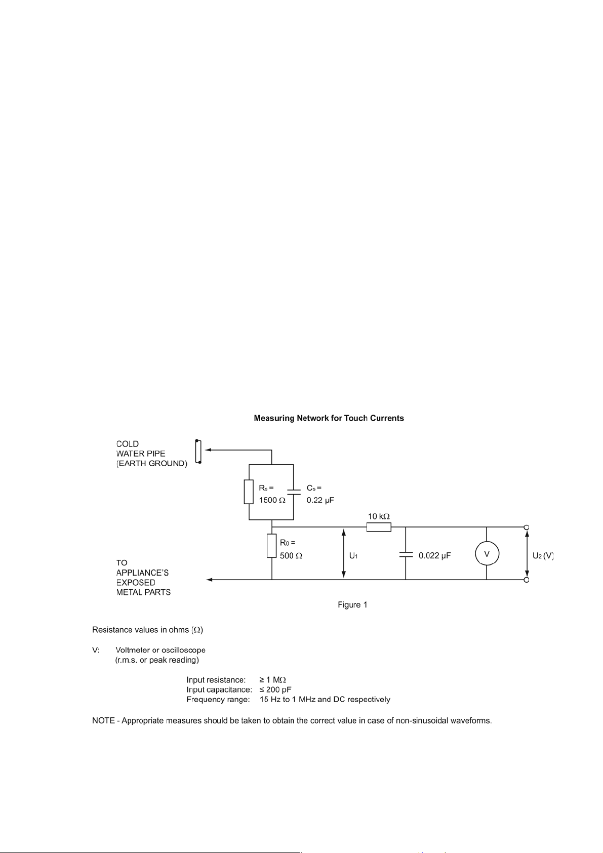
1.2. Touch-Current Check
1. Plug the AC cord directly into the AC outlet. Do not use an isolation transformer for this check.
2. Connect a measuring network for touch currents between each exposed me tallic part on the set and a good earth ground
such as a water pipe as shown in Figure 1.
3. Use the Leakage Current Tester (Simpson 228 or equivalent) to measure the potential across the measurin g network.
4. Check each exposed metallic part and measure the voltage at each point.
5. The potential at any point (touch current) expressed as voltage U
For AC: U1 = 35 V (peak) and U2 = 0.35 V (peak);
For DC: U
NOTE :
The limit value of U
DC.
The limit value U
= 1.0 V,
1
= 0.35 V (peak) for AC and U1 = 1.0 V for DC correspond to the values 0.7 mA (peak) AC and 2.0 mA
2
= 35 V (peak) for AC correspond to the value 70 mA (peak) AC for frequencies greater than 100 kHz.
1
and U2, do not exceed the following values:
1
6. Should a measurement be out of the li mits specified, there is a possibility of a shock hazard , and the equipment should be
repaired and rechecked before it is returned to the customer.
5

TX-LR19X10
TUNER
PWB
Hong Kong Digital
FE
S(5 or 6)/3.3
SDRAM
TUNER
TS
Parallel
ON Fix (Hard)
S5V
&
,
32 : (5
6:
P>CI_POWER_ON
P<CI_OCP
S3.3/1.8/1.2
M_SND
S5
M3.3
S3.3
S3.3
S3.3
A
V
-S
W
R2A11014FT
Video
Audio
SW
SLV[90]
HD/VD/FBK
MUTE
STB_XRST
5VS/STB5/S5/DTV12
S3.3
10MHz
S3.3/S5
S3.3
S3.3/S5
P> FE_SW
Opt
Digital OUT
CVBS
S3.3/S1.8
S9/S5
HP
AMP
MAIN
AMP
AV-OUT
MONITOR
OUT
CVBS
L/R
HP_OUT
L/R
AV-IN
YUV
CVBS/S
L/R
YUV
CVBS/S
L/R
CVBS
L/R
PC
RGB
HS/VS
ADV7470
SLV[40,etc]
HDMI-Rx *4
AD-IN
Y/CVBS
Pb/CPrRGB_CVBS
SOY
RGB_FB
PC_HS
PC_VS
INT
ADV_RESET
SIF
ADAV_RESET
S3.3/S1.8
HDMI
G>HPD
G<5V_DET
G<CEC
AV_L/R
MONITOR_OUT
L/R
AM
TV_L/R
L/R
L/R
L/R
MAIN
VIDEO
TU-CVBS
FE
WJCE6553
SLV[1E]
S5/S30
TUNER
SW1/2
mono
SIF
IF AGC
IF
PWM_OUT *1
Opt
SPDIF_OUT
CI
Card
TS
SW
3.3-5V
Level
Shift
TS
Buffer
CI
ASIC
#WE/#RE
#IOWR/#IORD
#REG
Buffer Ctrl
#CD
#IREQ
#WAIT
Peaks-LiteIIp
IIC0
IIC1
IIC2
IIC3
G> AUDIO_XRST
IRQ3
74.25MHz
27MHz
0+]
12MHz → nonuse
25MHzė IRU/$1
ICS
CLKGEN
w/t
VCXO
S1.8
TS
Serial
TS
Parallel
HSDIN
VI1CLKOUT
RGB 30bit
H,V,CLK
A
Po
rt
Video DAC
IECOUT
Audio
Discription
I2S
I2S
S3.3
Ana
l
og
ASIC
BD8651
GenX8
SLV[70]
SBO2
SBI2
EEPWP
IIC_1
SD-BOOT
STB3.3
E
EP 8
k
S
L
V
[
A
0
}
STB3.3
Su
p
por
t
card connector
NACE,CE1 CLE1
ALE1 WE1
RE1 WP BY
NOR Fla
sh
2
56Mbit
XRST
CS0
S3.3
STB3.3
OUT
RESET
HP
G> ADV_XRST
LVDS
USB-IF
TS
Parallel
PWMA
PWMK
LOSD
G> DTV_VOUTENB
Peaks L
i
teIIp S
y
st
e
m
MW: NONE
SD: ONBOARD
SD-IF
BLUE-LED: NONE
S3.3
E
EP 16
k
S
L
V
[
A0
}
S3.3
TE
MP SENSE
S
L
V
[
A
0
}
R
M
T/ K
EY
V-PWB
STB3.3/S5
G> G_LED_ON
G> R_LED_ON
G> ACTIVE_STBY_LED_ON
G< RMIN
G< AI_SENSOR
G< KEY1
IS0
CH0
FS
NONE
OVP
SOS
G>MON_MUTE
G>SP_HP_MUTE
AMP/HP_MUTE
MONITOROUT_MUTE
G< TV_SOS
P> CI_XRST
P> EEPROM_WP
G> EEPROM_WP
Peaks_XRST
Peaks POWER_DET
RESET
POWER_DET
DDR2
DDR2
CPU BUS
ADDRESS EA[25:24], EA[7:0]
DATA ED[15:0]
B
port / ADDRESS EA[23:8]
EA[23:8]
ED[15:0]
YC 16bit
H,V,CLK
ADDRESS
EA[25:0]
DATA
ED[15:0]
ADDRESS
EA[7:1]
DATA
ED[7:0}
ADDRESS
CI_EA[15:1]
DATA
CI_ED[7:0]
5-3.3V
Level
Shift
P> XETS_CI
S3.3/S5
P> FE1_IRQ
P< FE_XRST
MONITOROUT_MUTE
(G>MON_MUTE)
PWMA
PWMK
G>PWM_POW_ON
G<INVERTER_SOS
LVDS Single
PWM
ADIM
Filter
M9
LCD PANEL
G>INVERTER_ON
G>PANEL_TEST_ON
PNL_VCC
ADV
IIC
ADAV
IIC
24.576MHz to ADAV Block
ADV CLK from ADAV MCLK out
ADAV
MCLK
ADV CLK
30MHz
30.4MHz
TS
Serial
TS
Parallel
IIC_0
L/R
SP
G<SOUND_SOS
AMP/HP_MUTE
(G>SP_HP_MUTE)
SD-IF
NAND-IF
S3.3
1 $
1 ')OD
V
K
DATA
ED[7:0]
XNFCE,XNFWE,XNFRE
NFALE,NFCLE,XNFWP
NANDRYBY
S3.3
S
D
Card
P> FE_IRQ
P< FE_XRST
AMP/HP_MUTE
(G>SP_HP_MUTE)
PWM OUT *2
HP_OUT
PWM_READY
SPDIF_IN
DTV_I2S_IN
HDMI_I2S_SPDIF
OUT/IN
G> ADV_XRST
G>DTV_XRST
G>SW_OFF_DET
1.3. KM02 Chasis Block Diagram
6
TX-LR19X10
2 Prevention of Electro Static Discharge (ESD) to
Electrostatically Sensitive (ES) Devices
Some semiconductor (solid state) devices can be damaged easi ly by static electricity. Such components commonly are
called Electrostatically Sensitive (ES) Devices. Examples of typical ES devices are integrated circuits a nd some fieldeffect transistors and semiconductor “chip” components. The following techniques should be used to help redu ce the
incidence of component damage caused by electro static discharge (ESD).
1. Immediately before handling any semiconductor component or semiconductor-equipped assembly, drain off any ESD on your
body by touching a known earth ground. Alternatively, obtain and wear a commercially available discharging ESD wrist strap,
which should be removed for potential shock reasons prior to applying power to the unit under test.
2. After removing an electrical assembly equipped with ES devices, place the assembly on a conductive surface such as
aluminium foil to prevent electrostatic charge buildup or exposure of the assembly.
3. Use only a grounded-tip soldering iron to solder or unsolder ES devices.
4. Use only an anti-static solder removal device. Some solder removal devices not classified as “anti-static (ESD protected)” can
generate electrical charges sufficient to damage ES devices.
5. Do not use freon-propelled chemicals. These can generate el ectrical charges sufficient to damage ES devices.
6. Do not remove a replacement ES device from its protective package until immediately be fore you are ready to install it (most
replacement ES devices are packaged with leads electrically shorted together by conductive foam, aluminium foil or
comparable conductive material).
7. Immediately before removing the protective material from the leads of a replacement ES device, touch the protective material
to the chassis or circuit assembly into which the device will be installed.
Caution:
Be sure no power is applied to the chassis or circuit, and observe all other safety precautions.
8. Minimize bodily motions when handling unpackaged replacement ES devices (otherwise harmless motion such as the
brushing together of your clothes fabric or the lifting of your foot from a carpeted floor can gen erate static electricity (ESD)
sufficient to damage an ES device).
7

TX-LR19X10
3 About Lead Free Solder (PbF)
Note: Lead is listed as (Pb) in the periodic table of elements.
In the information below, Pb will refer to Lead Solder and PbF will refer to Lead Free Solder.
The Lead Free Solder (PbF) used in our manufacturing proce ss and discussed below is (Sn+Ag+Cu).
Those are Tin (Sn), Silver (Ag) and Copper (Cu), although other types are available.
This model uses PbF in its manufacture due to environmental conservation issues. For service and repair work, we would suggest
the use of PbF as well, although Pb may be used.
PCBs manufactured using lead-free will have the “PbF within a leaf Symbol” stamped on their back.
Caution
• PbF has a higher melting point than that of standard solder. Typically the melting point is 50 ~ 70°F (30~40°C) higher.
Please use a high temperature soldering iron and set it to 700 ± 20°F (370 ± 10°C).
• PbF will tend to splash when heated too high (about 1100°F or 600°C).
If you must use Pb solder, please completely remove all of the PbF on the pins or solder area before applyi ng Pb. If this is not
practical, be sure to heat the PbF until it melts, before applying Pb.
• After applying PbF to double layered boards, please check the component side for excess solder which may flow onto the
opposite side (see Figure 2).
Figure 2
Suggested PbF
There are several kinds of PbF available for purchase. This product uses Sn+Ag+C u (tin, silver, copper) solder. However, Sn+ Cu
(tin, copper) and Sn+Zn+Bi (tin, zinc, bismuth) solders can also be used.
Figure 3
8
4 Power LED Blinking Timing
1. Subject
Information of LED Flashing timing.
2. Contents
When an abnormality occurs, the protection circuit will operate and reset the unit to stand by mode. During this time, the
defective block can be identified by the number of blinking times of the Power LED on the front panel of the unit as follow:
Blinking times Contents
1 Inverter_SOS
3 SOS_3.3V over voltage protection
4 DTV_ 9V decreased / short circuit, main convertor stop detection.
5 Main_ 9V decreased
6 Sub_ 5V decreased
7 Sub_ 3.3V decreased
8 MAIN_ 3.3V decreased
9 Sound_ SOS
13 Emergency SOS
14 Audio PWM SOS
TX-LR19X10
9

TX-LR19X10
5 Location of Controls and Components
5.1. Wire Dressing
1. Wiring No.1 ~ No.2
2. Remove dust of terminal of LVDS and PB connector. (by ion blow)
Pos. A11
3. Insert LVDS into A11.
4. Make sure all connector wire fully insert.
Wire
No.1 P7
No.2 P6
= SINGLE CLAMP
= DOUBLE CLAMP
Clamper
TMME322
123
10
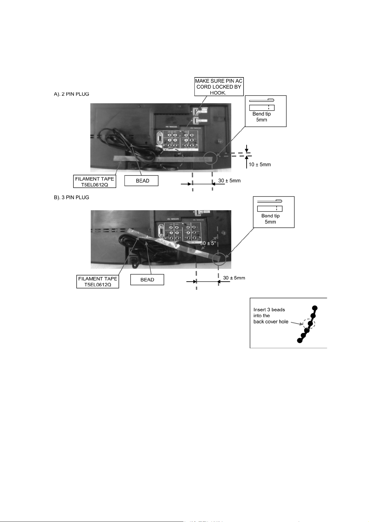
6 Disassembly and Assembly Instructions
6.1. AC Cord Dressing
Insert beads 3pcs. And slide down to lower hole.
TX-LR19X10
11

TX-LR19X10
6.2. AC Cord Installation
1. Put on the AC CORD BRACKET on the CABINET.
2. Fix the AC CORD BRACKET with SCREW.
3. AC CORD BARRIER setting.
4. Insert AC CORD connector into P-PCB connector.
5. Clamp the AC CORD.
6. Insert AC CORD bushing into the AC CORD BRACKET.
12

1. Put on the AC CODE BRACKET on the CABINET.
2. Fix the AC CODE BRACKET with SCREW.
3. Insert AC CODE connector into P-PCB connector.
4. Insert AC CODE bushing into the AC CODE BRACKET.
TX-LR19X10
13
TX-LR19X10
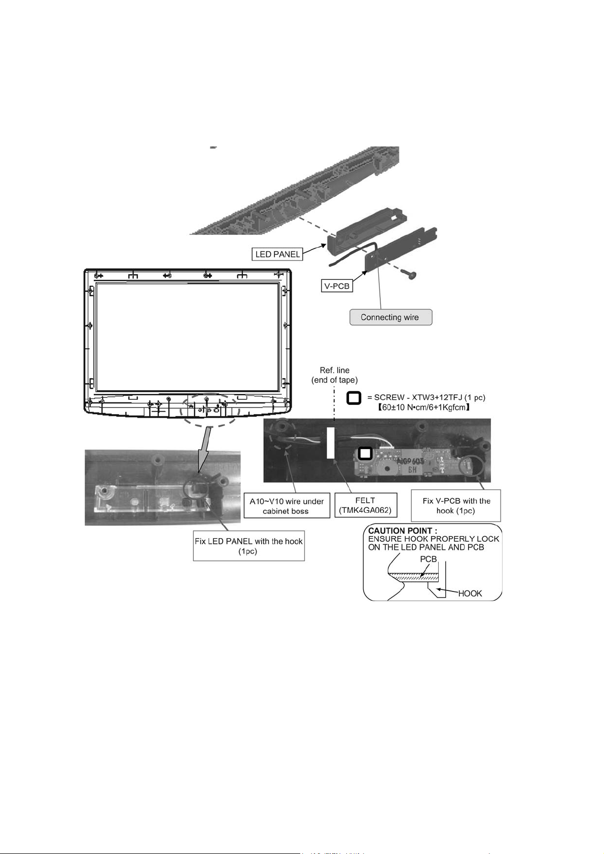
6.3. LED Panel Installation And Fitting
1. Fix LED PAN EL on CABINET.
2. Connecting wire (V10) V-PCB.
3. Put V-PCB on LED PANEL.
4. Fix them with SCREW.
5. Stick FELT (TMK4GA062) to A12 and A10 wire to cabine t.
14

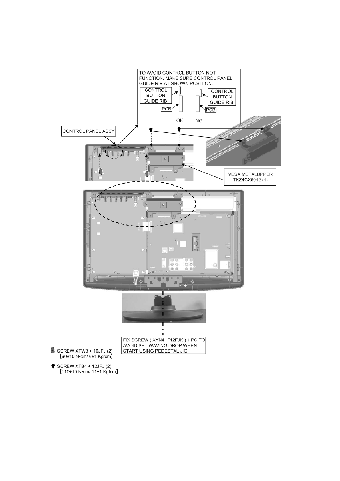
6.4. Control Panel Assembly
1. Fix FELT (TMK4G116) to CONTROL PANEL BRACKET.
2. Fix CONTROL BUTTON to CONTROL PANEL BRACKET.
- Fix them by screw (2 pcs).
3. Fix CONTROL PANEL ASSY cabinet.
- After fix P-BOARD, A-BOARD and TOP VESA METAL.
TX-LR19X10
15
TX-LR19X10
6.5. Control Panel Assembly and VESA Metal Installation
1. Put CONTROL PANEL ASSY.
- Fix them with SCREWS.
2. Put TOP VESA METAL.
- Fix them with SCREWS.
16

6.6. Side AV Bracket Assembly
Stick felt TMK4G028 (7 X 240 X 0.55t) - 2 PCS.
TX-LR19X10
17

TX-LR19X10
6.7. Speaker Installation
1. Fix SPEAKER to SPEAKER BRACKET .
- Fix them with SCREWS (4 pcs).
2. Fix SPEAKER ASSY to cabinet.
- Fix them with SCREWS (2 pcs).
18

6.8. EMI Spec (LVDS)
1. Insert LVDS wire to T-con conector, Make sure must center position follow below picture.
2. Stick FELT TMK4GA03 3 (15 X 60 X 0.55t) at LVDS wire (1 pc).
CAUTION.
Dressing LVDS wire to Panel must follow below instruction to avoid LVDS wire stuck in between chassis frame and panel.
TX-LR19X10
19

TX-LR19X10
6.9. Chassis and Frame Screw Position
20

6.10. Chassis Frame Fix to LCD Panel
1. Stick P-PCB BARRIER to chassis frame.
2. Fix chassis frame to LCD panel.
CAUTION
A - Make sure wire P6 and P7 not stuck between chassis frame and LCD panel
B - Terminal for P-board not stuck between chassis frame and LCD panel
C - Make sure wire A10~V10 and SP wire (L & R) not stuck between chassis frame and LCD panel
TX-LR19X10
1. Fix chassis frame to LCD panel
CAUTION
A - 1st.Put chassis frame at LCD panel at bottom side.
B - 2nd.Push to top side.
C - Make sure wire P6 and P7 not stuck between chassis frame and LCD panel
D - Terminal for P-board not stuck between chassis frame and LCD panel
2. Fix them with screw (4).
21

TX-LR19X10
6.11. Fix Chassis Frame and Cont. Panel Bracket
1. Fix CHASSIS FRAME to LCD PANEL ASSY with screw (4 pcs).
2. Fix LCD PANEL ASSY and CHASSIS FRAME to CABINET and fix by screw (2 pcs).
3. Fix CONTROL PANEL METAL BRACKET and fix by screw (1 pc).
22

6.12. Power Button, Top VESA Metal and Cont. Panel Assembly
1. Fix POWER BUTTON to power switch (P-board).
- fix P-BOARD to chassis frame.
3. Fix TOP VESA METAL to cabinet.
4. Fix CONTROL PANEL ASSY to cabinet.
TX-LR19X10
2. Fix A-BOARD to chassis frame.
- Insert LVDS wire to A-BOARD conector, make sure in
center position follow below picture.
23

TX-LR19X10
6.13. VESA (BC) Installation
1. Put VESA METAL (BC) on the BACK COVER.
2. Fix them with SCREWS.
24

TX-LR19X10
25

TX-LR19X10
6.14. Pedestal Assembly
Step 1
1. Setting HINGE BRACKET and BASE PLATE with SCREWS.
2. Setting PEDESTAL COVER and BASE PLATE with SCREWS.
Step 2
1. Stick the RUBBER FOOT at bottom BASE PLATE.
2. RUBBER FOOT (TBL4GG3005 - 4 pcs) stick at BASE PLATE.
26

TX-LR19X10
7 Service Mode Adjustment
Set timer to 30min, press the “RECALL” button on the remote control and press “-” vol button on the LCD panel.
• Press button R and G for adjustment.
7.1. Self Check Mode
1. Press the “MENU” button (on the remote control) and the “DOWN” button on the LCD panel.
2. Press ON/OFF button on the panel to Exit.
7.2. Hotel Mode Adjustment
1. Press the “VOLUME DOWN” button on the TV panel and simultaneously press the AV button on the remote control 3 times to
enter Hotel Mode.
2. Set Hotel mode “on/off”, then press “EXIT” to come out.
7.3. Hotel Mode
1. Purpose
Restrict a function for hotels.
2. Access command to the Hotel mode setup menu.
In order to display the Hotel mode setup menu, please
enter the following command (within 2 second).
[TV] : Hold Vol [Down] + [Remote] : Press AV button 3
times.
Then, the Hotel mode setup menu is displayed.
Item Function
Hotel Mode Select hotel mode ON/OFF
Initial INPUT Select input signal modes.
Set the input, when each time power is switched
on.
Selection :
OFF/Analogue TV/Digital TV/AV1/AV2/AV3//PC/
HDMI1/HDMI2/HDMI3
• Off: give priority to a last memory.
• Selectable input is depend on the model.
Initial POS Select programme number.
Selection :
Off/0 to 100
• Off: give priority to a last memory.
Initial VOL level Adjust the volume when each time power is
switched on.
Selection/Range :
Off/0 to 100
• Off: give priority to a last memory.
Maximum VOL
level
Button lock Select local key conditions.
Remote lock Select remote control key conditions.
Adjust maximum volume.
Range :
0 to 100
Selection :
Off/SETUP/MENU/All
• Off: altogether valid.
• SETUP: only F-key is invalid.
(Tuning guide (menu) can not be selected.)
• MENU: only F-key is invalid.
(only Volume/Mute can be selected.)
• ALL: altogether invalid.
Selection :
Off/SETUP/MENU
• Off: altogether valid.
• SETUP: only Setup menu is invalid.
• MENU: Picture/Sound/Setup menu are invalid.
27

TX-LR19X10
8 Measurements and Adjustments
8.1. Voltage Check
Set IP-Board to a dummy set and check the satisfaction with the specified voltage as following table.
Power Supply Name Measurement Point Normal Condition (V) Standby Condition (V)
AUDIO_VCC TPP020 17.0 ± 1.5 NO CARE
12V TPP003 12.0 + 0.6 / -0.45 < 1.0
5VS TPP010 6.1 ± 0.3 6.1 ± 0.3
STBY_6V TPP016 6.1 ± 0.3 6.1 ± 0.3
After inspection, discharge the C828(26”) or C810(19”) with 1kΩ resistor for 0.3 sec. or more
In IP-PCB only, load condition is following
Power Supply Name Dummy Load Range Resistor Load
AUDIO_VCC 0 - 1.5A 11 ohm
12V 0.5 - 2.2A 5.6 ohm
5VS 0 - 1.3A 4.3 ohm
STBY_6V 0 - 0.05A 100 ohm
8.2. Power Supply for Writing Data in Board Indivisual.
Power Supply Name TP No. Voltage (V)
5VS TP2765 5.5 +/- 2%
STB5V TP2771 5.5 +/- 2%
SUB_TNR_6V TP2770 5.5 +/- 2%
P17V TP2763 17 +/- 2%
SUB_F_12V TP2764 12 +/- 2%
GND TP2766 0
About start up sequence of power supply
Start up other power supplies after starting up STB5V.
8.3. White Balance
Ambient Temp. Colour Balance
Cool 0.271 0.275 >150 0.271 0.275
22.5 - 27.5 deg
Warm 0.314 0.324 >150 0.314 0.324
x y Y (cd/m2) x y Y (cd/m2)
x, y : +/-0.005 in Normal Colour Balance, +/-0.020 in Wa rm/Cool Colour Balance
White Gray
don’t careNormal 0.284 0.297 >200 0.284 0.297
28

9 Printed Circuit Board
1
A
B
C
D
E
F
G
H
I
J
K
L
2 3 4 5 6 7 8 9 10
M
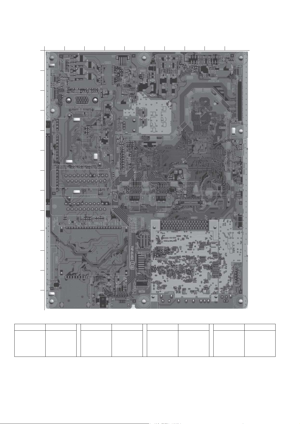
9.1. A-Board
A-Board (A Side)
TNP4G460
TX-LR19X10
Parts Location
Ref. No Location Ref. No Location Ref. No Location Ref. No Location
IC1100 K4 IC5441 M9 IC8404 J4 D3015 D7
IC1101 L3 IC5480 J5 IC8405 J3 D4513 H7
IC2750 L2 IC5600 B5 IC8408 J3 D4617 L8
IC2901 K10 IC5601 B5 IC8409 L2
IC2902 K9 IC8004 D4 IC8410 J2
IC3001 D8 IC8301 K8 IC8554 G3
IC4513 G7 IC8302 L8 IC8601 H5
IC5405 B4 IC8401 H2
29
TX-LR19X10
1
A
B
C
D
E
F
G
H
I
J
K
L
2 3 4 5 6 7 8 9 10
M
9.2. A-Board
A-Board (B Side)
TNP4G460
Ref. No Location Ref. No Location Ref. No Location Ref. No Location
IC2008 E4 IC4512 G7 IC8002 C8 D3015 E5
IC2301 A4 IC5409 B5 IC8003 D9
IC4510 F5 IC5451 B9 IC8403 F10
IC4511 G7 IC8001 E9 IC8411 L9
Parts Location
30
 Loading...