

PANASONIC TC 20KL05P Service Manual
ORDER DCS - SEP2005 - 004 - MS
Service Manual
Color Television
TC-20KL05P
Chassis GP31
Specifications
TELEVISION
Power souce
Consumption
Antenna imput
Color sytem
Tuning system
Channel capability
Picture tube
Imput
Imput jack
A V Terminals
Dimension (WxHxD)
Weigth
REMOTE CONTROL TRANSMITER:
Model: TNQ2B2801-1
Power source: 3V (2 AA type batteries)
Infrared wave lenght 9500 Å (Angstron)
TC-20KL05P
127V / 220V AC, 60Hz
automatic switch
61W
75Ω - VHF/UHF/CATV
PAL-M / NTSC / PAL-N
(FST)
VHF: 2 ~13
UHF: 14 ~ 69
CATV : 1 ~ 125
PANABLACK
20” CRT, 51cm (NBR5258)
Measured diagonally
48cm
3 W max (PMPO)
1 ( rear)
514 x 468x 461mm
17,0 Kg
Supplied accessories:
• 1 remote control transmitter
• 1 Balum 300 ohms / 75 ohms
• 2 “AA” (or R6) batteries (1.5 V; ABNT/IEC)
• 1 antenna
Specifications are subject to change without prior notice or obligation.
© 2005 Panasonic da Amazônia S/A.
CS Division
Technical Support
TC-20KL05P
Important Safety Notice
Special components are used in this television set which are important for safety. These parts are identified on the schematic
diagram by the symbol . It is essential that these critical parts are replaced with the manufacturer’s specified replacement
parts to prevent X-ray radiation, shock, fire or other hazards. Do not modify the original design without manufacturer’s permission.
!
Contents
ABOUT LEAD FREE SOLDER (PBF) ........................................................ 3
SUGGESTED PBF SOLDER .................................................................... 3
HOW TO RECOGNIZE THAT PB FREE SOLDER IS USED ......................... 3
IC601 - PINOUT ...................................................................................... 5
IC601 - PINOUT ....................................................................................... 6
IC VOLTAGE TABLES ............................................................................. 6
IC601 - BLOCK DIAGRAM ...................................................................... 7
GP31 CHASSIS FEATURE SUMMAR Y .................................................... 8
DAC CONTROL FOR GP31 CHASSIS FUNCTIONS AND ADJUSTMENTS ......... 9
HOW TO RESET THE UNIT (SELF CHECK) ............................................... 9
HOW TO ENTER IN THE SERVICE MODE ................................................. 9
CHK1 MODE - OPTIONS ......................................................................... 9
ADJUSTMENTS ....................................................................................... 10
CHK2 MODE - VCJ ADJUSTMENTS ....................................................... 10
CHK3 MODE - PINCUSHION ADJUSTMENTS ......................................... 10
EEPROM MEMORY MAPS ...................................................................... 1 1
ADJUSTMENTS ....................................................................................... 13
CRT P.C.B. .............................................................................................. 18
SCHEMATICS DIAGRAMS ....................................................................... 18
SHEMATIC DIAGRAM P.C.B. ................................................................... 19
MAIN P .C.B. ............................................................................................. 20
SIGNAL WA VEFORM .............................................................................. 21
EXPLODED VIEW .................................................................................... 25
REPLACEMENT MECHANICAL PARTS LIST .......................................... 26
REPLACEMENT ELECTRICAL P ARTS LIST ............................................ 27
General Guidelines
An Isolation Transformer should always be used during the servicing
of a receiver whose chassis is not isolated from the AC power line.
Use a transformer of adequate power rating as this protects the
technician from accidents resulting in personal injury from electrical
shocks. It will also protect the Receiver from being damaged by
accidental shorting that may occur during servicing.
When servicing, observe the original lead dress, especially in the high
voltage circuit. Replace all damaged parts (also parts that show signs
of overheating.)
Always Replace Protective Devices, such as fishpaper, isolation
resistors and capacitors, and shields after servicing the Receiver.
Use only manufacturer’s recommended rating for fuses, circuit
breakers, etc.
High potentials are present when this Receiver is operating. Operation
of the Receiver without the rear cover introduces danger from electrical
shock. Servicing should not be performed by anyone who is not
thoroughly familiar with the necessary precautions when servicing
high-voltage equipment.
Extreme care should be practiced when Handling the Picture Tube.
Rough handling may cause it to implode due to atmospheric pressure
(14.7 lbs per sq. in). Do not sick or scratch the glass or subject it to
any undue pressure. When handling, use safety goggles and heavy
gloves for protection. Discharge the picture tube by shorting the anode
to chassis ground (not to the cabinet or to other mounting hardware).
When discharging, connect cold ground (i.e. dag ground lead) to the
anode with a well insulated wire or use a grounding probe.
Avoid prolonged exposure at close range to unshielded areas of the
picture tube to prevent exposure to X-ray radiation.
The Test Picture Tube used for servicing the chassis at the bench
should incorporate safety glass and magnetic shielding. The safety
glass provides shielding for the tube viewing area against X-ray radiation
as well as implosion. The magnetic shield limits X-ray radiation around
the bell of the picture tube in addition to restricting magnetic effects.
When using a picture tube test jig for service, ensure that the jig is
capable of handling 31kV without causing X-ray radiation.
Before returning a serviced receiver to the owner, the service
technician must thoroughly test the unit to ensure that is completely
safe to operate. Do not use a line isolation transformer when testing.
- 2 -
!
Warning !
It is essential that these critical parts are replaced
with the manufacturer’s specified replacement parts
to prevent X-ray radiation, shock, fire or other hazards.
TC-20KL05P
ABOUT LEAD FREE SOLDER (PbF)
Note:
In the information below, Pb, the symbol for lead in the periodic table of elements, will refer to standard solder or solder that
contains lead.
We will use PbF solder when discussing the lead free solder used in our manufacturing process which is made from Tin (Sn),
Silver, (Ag), and Copper, (Cu).
This model, and others like it, manufactured using lead free solder will have PbF stamped on the PCB. For service and repair
work we suggest using the same type of solder although, with some precautions, standard Pb solder can also be used.
Caution
• PbF solder has a melting point that is 50° ~ 70° F, (30° ~ 40°C) higher than Pb solder. Please use a soldering iron with
temperature control and adjust it to 700° ± 20° F, (370° ± 10°C).In case of using high temperature soldering iron, please be
careful not to heat too long.
• PbF solder will tend to splash if it is heated much higher than its melting point, approximately 1100°F, (600°C).
• If you must use Pb solder on a PCB manufactured using PbF solder, remove as much of the original PbF solder as possible
and be sure that any remaining is melted prior to applying the Pb solder.
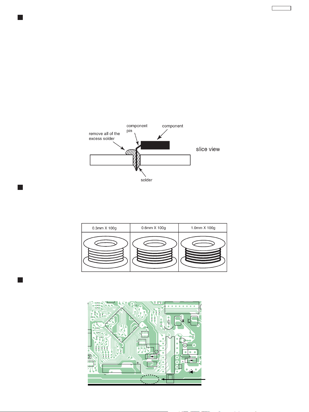
• When applying PbF solder to double layered boards, please check the component side for excess which may flow onto the
opposite side (See figure, below).
SUGGESTED PbF SOLDER
There are several types of PbF solder available commercially. While this product is manufactured using Tin, Silver, and Copper,
(Sn+Ag+Cu), you can also use Tin and Copper, (Sn+Cu), or Tin, Zinc, and Bismuth, (Sn+Zn+Bi). Please check the manufac
turer’s specific instructions for the melting points of their products and any precautions for using their product with other
materials.
The following lead free (PbF) solder wire sizes are recommended for service of this product: 0.3mm, 0.6mm and 1.0mm.
HOW TO RECOGNIZE THAT PB FREE SOLDER IS USED
P.C.Boards marked as “PbF” use Pb Free solder. (See the figure below.) Pb Free is not used the Power Supply Board of this
unit.
(Example : Digital Board)
L624
L625
L626
L660
L661
L658
L659
100
C694
L653
L655
L657
L654
L656
1
L642
R768
L605
H
RA602
PFUP1330YA PbF
R767
R769
L606
L604
Q609
75
76
IC605
2625
C666
L643
BAT600
R70
C738
51
50
C667
RA609
D602
C668
RA610
C672
C731
L620
L619
L618
+3.3V/BAT
J600
C717
L621
R723
L630
1
R708
8
C728
IC610
+24V
CN612
16
9
Q613
E
R736
F605
25
18
R613R610
R611
R737
E
Q620
D608
C726
D607
Marked
DIGITAL BOARD COMPONENT VIEW
- 3 -
TC-20KL05P
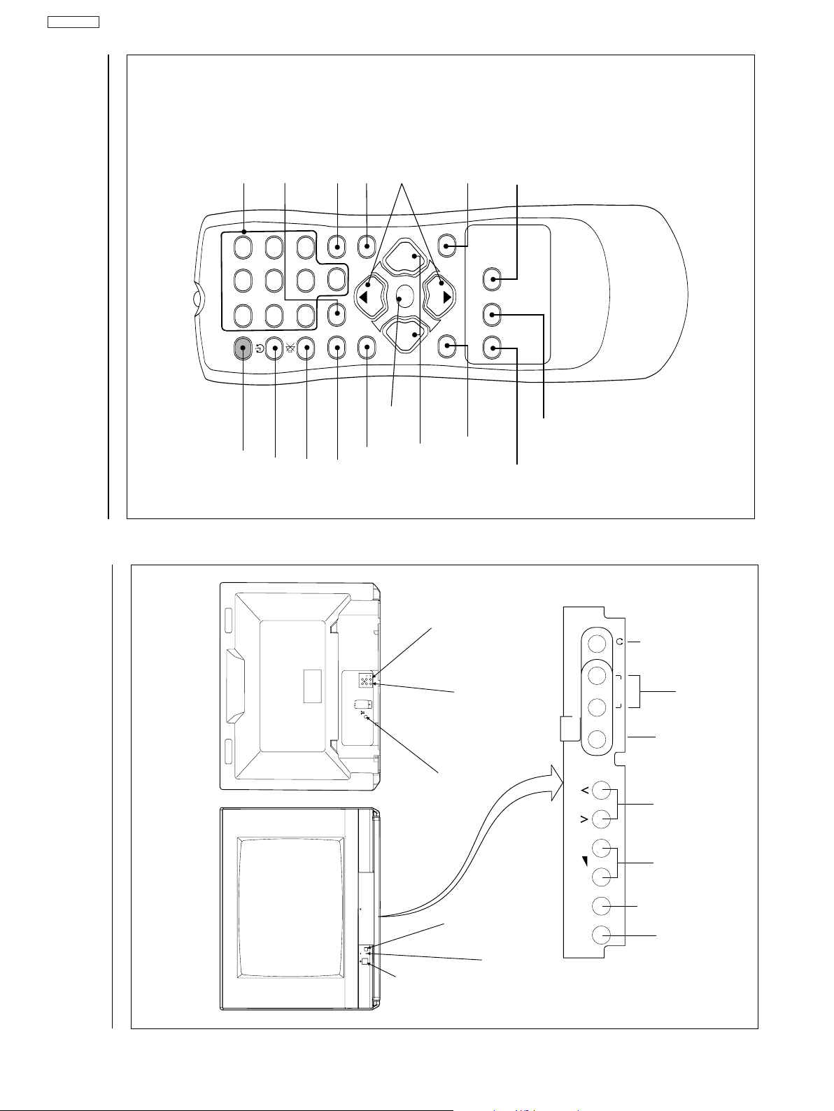
Location of Controls
CHANNELS
KEYBOARD FOR
DIRECT SELECTION
WAKE UP
R-TUNEWAKE U PTV/AV
R-TUNE
CLOSED CAPTION
CC
CHANNELS
SELECTION AND
MENU NAVIGATION
MAIN MENU
MAIN MENU
SURROUND
0
N
N
CH
CH
123
456
789
u
POWER
TIMER
Remote Control
MUTE
e
TV/AV
RECALL
NORMALIZATION
VOL– VOL+
VOL– VOL+
VOLUME
CH
CH
SOUND
PIC MENU
PIC MENU
AND MENU
NAVIGATION
MENUSAP SURROUND
SAP
SOUND MENU
Panasonic
Location of Controls
input jack
Audio/Video
R
L
VÍDEO
ÁUDIO
SAÍDAENTRADA
MONITOR MONO
Back View
output
Audio/Video
L/MONO R
AUDIO
VIDEO
output
Earphone
input
Video
Audio
input
AV IN
Antenna
input jack
buttons
Channel
–+
Panasonic
Front View
switch
Powe r
control
Remote
sensor
MENU TV/AV
Indication light
TV/AV button
buttons
Volume
MENU
button
- 4 -

TC-20KL05P
IC601 - PINOUT
Symbol Pin Description
P3.1/ADC1 1 port 3.1 or ADC1 input
P3.2/ADC2 2 port 3.2 or ADC2 input
P3.3/ADC3 3 port 3.3 or ADC3 input
VSSC/P 4 digital ground for m-Controller core and periphery
P0.5 5 port 0.5 (8 mA current sinking capability for direct drive of LEDs)
P0.6/CVBSTD 6 port 0.6 (8 mA current sinking capability for direct drive of LEDs) or Composite video input. A positive-going
VSSA 7 digital ground of TV-processor
SECPLL 8 SECAM PLL decoupling
VP2 9 2nd supply voltage TV-processor (+8V)
DECDIG 10 supply voltage decoupling of digital circuit of TV-processor
PH2LF 11 phase-2 filter
PH1LF 12 phase-1 filter
GND3 13 ground 3 for TV-processor
DECBG 14 bandgap decoupling
AVL 15 Automatic volume levelling
VDRB 16 vertical drive B output
VDRA 17 vertical drive A output
IFI N1 18 IF input 1
IFI N2 19 IF input 2
IREF 20 reference current input
VSC 21 vertical sawtooth capacitor
AGCOUT 22 tuner AGC output
NC 23 Not connected
NC 24 Not connected
GND2 25 ground 2 for TV processor
SNDPLL 26 narrow band PLL filter
IC 27 Inter nally connected
AUDIO2 28 audio 2 input
AUDIO3 29 audio 3 input
HOUT 30 horizontal output
FBISO 31 flyback input/sandcastle output
DECSDEM 32 decoupling sound demodulator
AUDEEM 33 Deemphasis (front-end audio out)
EHTO 34 EHT/overvoltage protection input
PLLIF 35 IF-PLL loop filter
IC 36 Internally connected
IC 37 Internally connected
IFVO/SVO 38 IF video output / selected CVBS output
VP1 39 main supply voltage TV processor
CVBS1 40 internal CVBS input
GND 41 ground for TV processor
CVBS2 42 external CVBS2 input
GND 43 ground for TV-processor
CVBS3/Y 44 CVBS3/Y input
C 45 chroma input
WHSTR 46 white stretch capacitor
CVBSO 47 CVBS output
AUDOUT 48 Audio output
NC 49 Not connected
INSSW2 50 2nd RGB / YUV insertion input
R2/VIN 51 2nd R input / V (R-Y) input / PR input
G2/YIN 52 2nd G input / Y input
B2/UIN 53 2nd B input / U (B-Y) input / PB input
BCLIN 54 beam current limiter input
BLKIN 5 5 black current input / V-guard input
RO 56 Red output
GO 57 Green output
BO 58 Blue output
VDDA 59 analog supply of Teletext decoder and digital supply of TV-processor (3.3 V)
- 5 -
TC-20KL05P
IC601 - PINOUT
Symbol Pi n Description
VP E 60 OTP Programming Voltage
VDDC 61 digital supply to core (3.3 V)
OSCGND 62 oscillator ground supply
XTALIN 63 crystal oscillator input
XTALOUT 64 crystal oscillator output
RESET 65 reset
VDDP 66 digital supply to periphery (+3.3 V)
P1.0/INT1 67 port 1.0 or external interrupt 1 input
P1.1/T0 68 port 1.1 or Counter/Timer 0 input
P1.2/INT0 69 port 1.2 or external interrupt 0 input
P1.3/T1 70 port 1.3 or Counter/Timer 1 input
P1.6/SCL 71 port 1.6 or I2C-bus clock line
P1.7/SDA 72 port 1.7 or I2C-bus data line
P2.0/TPWM 73 port 2.0 or Tuning PWM output
P2.1/PWM0 74 port 2.1
P2.2/PWM1 75 port 2.2
P2.3/PWM2 76 port 2.3
P2.4/PWM3 77 port 2.4
P2.5/PWM4 78 port 2.5
Sync F. 79 Sync Filter
P3.0/ADC0 80 port 3.0 or ADC0 input
IC VOLTAGE TABLES
Pin Vol tage
1 3,3
2 5,0
3 1,8
40
5 4,5
60
70
8 2,3
9 8,0
10 5,0
11 3,2
12 4,0
13 0
14 4,0
15 0,2
16 1,3
17 1,3
18 1,9
19 1,9
20 4,0
21 3,8
22 0
23 0
24 0
25 0
26 0
27 2,5
28 3,7
29 3,7
30 0,6
31 0,6
32 2,2
33 3,1
34 1,6
35 1,5
36 2,4
37 1,5
38 2,8
39 8,0
40 3,6
IC601
Pin Vol tage
41 0
42 3,8
43 0
44 3,3
45 0
46 3,5
47 3,0
48 3,3
49 0
50 2,5
51 2,5
52 2,5
53 2,5
54 2,0
55 5,3
56 4,0
57 3,8
58 3,8
59 3,3
60 0
61 3,3
62 0
63 1,6
64 1,6
65 0
66 3,3
67 3,3
68 5,0
69 5,0
70 3,2
71 0
72 5,0
73 0
74 0,2
75 0
76 0
77 0
78 0
79 0
80 0
IC451
Pin Vol tage
1 0,3V
2 0,14V
3 -12V
4 -14V
50V
6 15V
73V
IC1201
Pino Tensã o
15V
20V
3 1,27V
4 3,3V
50V
65V
IC801
Pin Vol tage
1 187V
3 0,5V
4 22,5V
5 0,1V
6 1,3V
7 0,5V
IC2301
Pino Ten são
1 11,5V
25V
30V
45V
5 2,8V
6 1,5V
70V
80V
9 0,5V
IC851
Pin Vol tage
1 10,7V
2 10,7V
3 3,3V
40V
5 3,1V
68V
75V
IC802
Pin Vol tage
1 141V
29V
30V
Pin Vol tage
All voltage measurements were made in POWER ON mode, with 127V 60Hz power
source and Color Bars Video Pattern.
IC880
1 10,4V
25V
30V
- 6 -

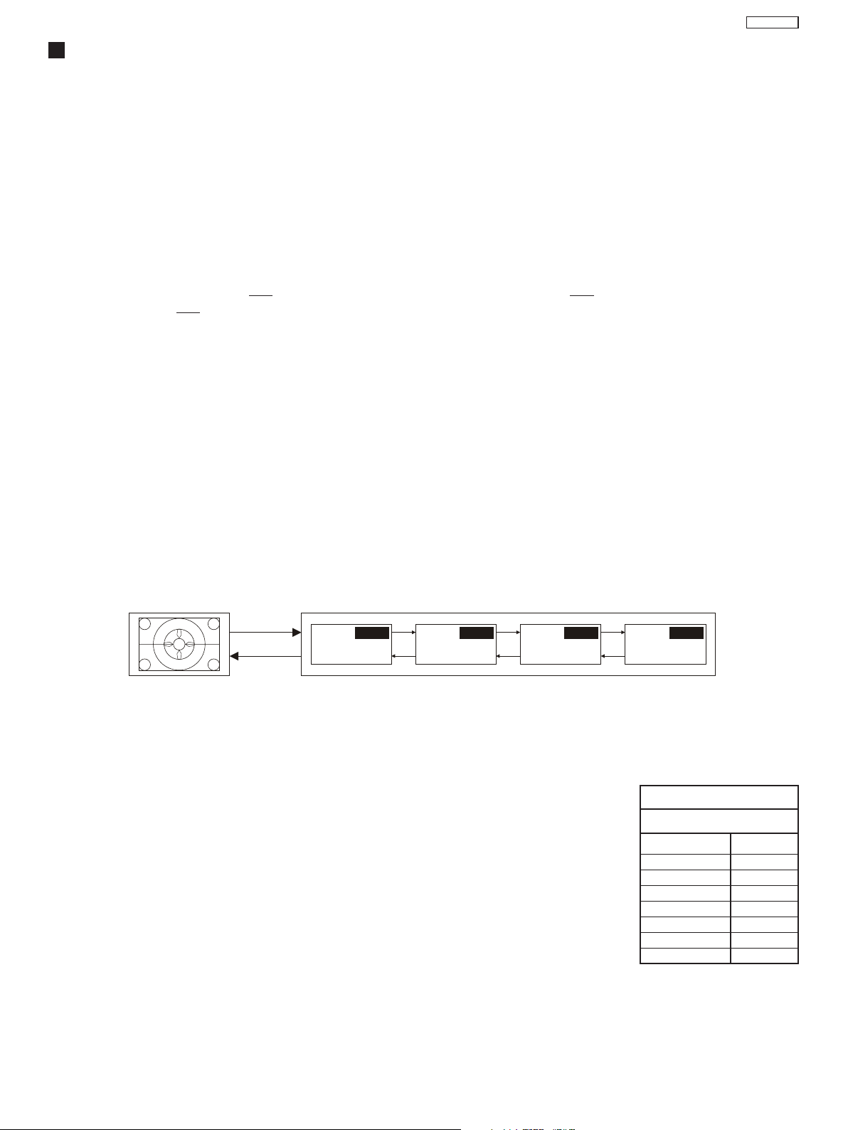
IC601 - BLOCK DIAGRAM
TC-20KL05P
+3.3 V
PWMS(4X)
I/O PORTS (4x)
ADC IN (4x)
VST OUT
SDASCL
LED OUT (2x)
VPE
RESET
AUDOUT
AUDIO3
AUDIO2
1/10 PAGE
MEMORY
C-BUS
2
I
TRANSCEIVER
VST PWM-DAC
80C51 CPU
ENHANCED
I/O PORTS
DISPLAY
TELETEXT/OSD
V
H
TELETEXT
ACQUISITION
CVBS
ROM/RAM
ROGOBO
BL
B
RG
CONTR/BRIGHTN
OSD/TEXT INSERT
COR
SYNC
DELAY LINE
BASE-BAND
BLKIN
BCLIN
GB
CCC
R
WHITE-P. ADJ.
BLUE STRETCH
TINT CONTROL
SATURATION
BLACK STRETCH
RGB/YUV INSERT
WHITE STRETCH
Y
U
V
EW GEOMETRY
V-DRIVE +
GEOMETRY
V
G/Y B/U BL
R/V
(EWD)
EHTO
VMOUT
HOUT V-DRIVE
(AVL)
(SNDIF)
AUDEEM
QSSO/AMOUT
AVL
SOUND PLL
DEEMPHASIS
AUDIO SWITCH
VOLUME CONTROL
AGC
QSS MIXER
QSS SOUND IF
AM DEMODULTOR
SIFIN
LUMA DELAY
REF
VISION IF
PLL DEMOD.
VIFIN
TUNERAGC
PEAKING
VMOUT
AGC/AFC
VIDEO AMP.
- 7 -
PAL/SECAM/NTSC
REF
VIDEO SWITCH
IFVO
TRAP
SOUND
DECODER
VIDEO IDENT.
VIDEO FILTERS
CVBS3/Y
CVBS2
C
CVBSO
Y
LOOP
nd
H-DRIVE
H-SHIFT
2
H
H-OSC. + PLL
H/V SYNC SEP.
+8V
TC-20KL05P
GP31 CHASSIS FEATURE SUMMARY
CHASSIS : GP31
MODEL : TC-20KL05P
SYSTEM : 3 system (P AL-M/P AL-N/NTSC) (PAL-M 50Hz)
POWER SOURCE : AC automatic power switching (127/220)V , 50/60Hz
MEMORY : 125 positions
TV TUNING RANGE : 181 channels (TV / CATV)
OSD LANGUAGE : Sp anish , Portuguese and English
AUDIO SYSTEM : Mono
VERTICAL MAGNEGTIC FELD : -0.1 ± 0.03 (P ANALAT)
COLOR TEMPERATURE : (High Light) x= 0.275±0.01, y=0.284 ±0.01, Y=150 (nit))
(Low Light) x= 0.273±0.01, y=0.283 ±0.01, Y=7.0 (nit)
REFERENCE VOLTAGE
CONTENTS REFERENCE TEST POINT
+B VOLTAGE
Sound confirmation
PAL color output
NTSC color output
Anode (EHT) voltage
Memory Data
002
007
009
010
008
[A]=C0H, [B]=00H, [C]=00H, [D]=B3H, [E]=06H, [F]=01H, [G]=00H, [H]=09H
Between A22-1 an d A22-3
TPA10
TPA8
TPA9
TPA21
or A22-2 and A22-4
TPL2
TPL1
TPL1
CRT
ANODE
POINTS
D
C
C
SPECIFICATIONS
140 ± 1,5V
8 ±1V
5 ±1V
175 ±1V
0.5 Vp-p
2.25 ±0.1Vo-p
2.25 ±0.5Vo-p
2.5 ±0.5Vo-p
26.5 +0.7 (kV)
26.5 -1.5 (kV)
- 8 -
TC-20KL05P
DAC CONTROL FOR GP31 CHASSIS FUNCTIONS AND ADJUSTMENTS
HOW TO RESET THE UNIT (SELF CHECK)
To reset the unit, press simultaneously “VOLUME (–)” on the front panel and “TIMER” on the remote control.
HOW TO ENTER IN THE SERVICE MODE:
1. Adjust “OFF TIMER” to 30 minutes.
Press simultaneously “VOLUME (–)” on the front panel and “RECALL” on the remote control to enter “SERVICE
MODE”.
After a couple of seconds, the expression “CHK1” should appear on the right superior side of the TV screen.
2. To change to memory data, press ”MUTE” and ”VOLUME(_)” simultaneously while the OSD is still on CHK1 mode.
3. Press key “2” to move forward and “8” to move backward each page (8h positions) in the memory .
Exemple: Memory position is 100. Af ter pressing “2” the cursor will go to position 0F8 and after pressing “8” the cursor
will go to position 108 .
4. Press “4” and “6” to move to right or left.
5. Press “CH(+)” e “CH(–)” to move for blocks.
Example: Initial memory position is 000. By pressing “CH(+)” cursor will go to position 100, pressing it once again the
cursor will go to position 200. The key “CH(–)” does the inverse move.
6. To change values in the memory , press “VOLUME(+)” to increase and ”VOLUME(_)” to decrease.
7. After data adjustment, OSD will change to RED color . Press “0” to memorize the adjustment and the OSD will change to
GREEN color.
NOTE:
To alter from CHK1 mode to CHK2, CHK3 or CHK4 mode, press key “2” to move forward and key “1” to move back, as
ilustrad below.
NORMAL MODE SERVICE MODE
Turn Off
OPTION CODE
CHK1
SETTING
“2”
ADJUSTMENT
1
”
“
VCJ
“2”“
CHK2 CHK3 CHK4
PINCUSHION
ADJUSTMENT
1
”“
“
2
”
WHITE BALANCE
ADJUSTMENT
1
”
CHK1 MODE - OPTIONS
On CHK1 mode it is possible to adjust the items of the table shown here.
Note:
T o select an option, type “4” to move forward and “3” to move back.
After having selected the desired option, adjust it by pressing the “VOL(_)” or “VOL(+)”
keys.
Press “0” to memorize the adjustment.
Observation:
V alues of CHK1 table in should be programed, exactly as described in the t able
shown here.
TABLE CHK1
Values
OPTION1
OPTION2
OPTION3
OPTION4
OPTION5
OPTION6
OPTION7
OPTION8
C0
00
00
B3
06
01
00
09
- 9 -
TC-20KL05P
ADJUSTMENTS
CHK2 MODE - VCJ ADJUSTMENTS
On CHK2 mode it is possible to adjust the items of the table shown here.
Note:
To select an item, type “4” to move forward and “3” to move back.
After having selected the desired option, adjust it by pressing the “VOL(_)” or
“VOL(+)” keys.
CHK3 MODE - PINCUSHION ADJUSTMENTS
On CHK3 mode it is possible to adjust the items of the table shown here.
Note:
To select an item, type “4” to move forward and “3” to move back.
After having selected the desired option, adjust it by pressing the “VOL(_)” or
“VOL(+)” keys.
CHK4 MODE - WHITE BALANCE ADJUSTMENTS
On CHK4 mode it is possible to adjust the items of the table shown here.
Note:
To select an item, type “4” to move forward and “3” to move back.
After having selected the desired option, adjust it by pressing the “VOL(_)” or
“VOL(+)” keys.
CHK2 MODE T ABLE
Reference values
RF AGC
CONTRAST
COLOUR
SUB COLOUR
TINT
SUB NTSC-TINT
BRIGHT
CHK3 MODE TABLE
Reference values
V-SLOPE
V-SHIFT
V-AMP
H-SHIFT
CHK4 MODE T ABLE
Reference values
R-CUT
G-CUT
BRIGHT
SUB-BRIGHT
CONTRAST
SUB- CONTRAST
R-DRIVE
G-DRIVE
B-DRIVE
RGB-CONTRAST
23
100
50
28
50
28
50
32
37
43
45
28
30
50
30
100
11
33
31
35
2
Observation:
The values of the tables CHK2, CHK3 and CHK4 are reference values and they can vary , according to each receiver.
TO EXIT SERVICE MODE AND RETURN TO NORMAL MODE
To exit SERVICE MODE, turn off or reset (SELF CHECK) the television.
- 10 -
 Loading...