

Page 1
ORDER No.AD0101008C2
Portable MD Player
SJ-MJ88
MD unit: RAE1611Z Mechanism Series
Colour
(S)...................Silver Type
Areas
EB...................Great Britain.
EG...................Europe.
1
Page 2

SPECIFICATIONS
Audio
System:MiniDisc digital audio
Laser:Semiconductor laser (=780
Sampling frequency:44.1 kHz
Coding:Adaptive Transform
No. of channels:2 (left and right, stereo)
Frequency response:20 Hz~20 kHz (+0 dB, -8dB)
Wow and flutter:Below measurable limit
General
Output terminal
Output Jack:Phones, 22
Power output:3.5 mW+3.5
Power supply
Rechargeable
battery:
Battery:DC 1.5V (One LR6, AA, UM-3
Dimensions (WxHxD)
Cabinet dimensions:71.5x78.5x11.8 mm
Specifications
system
nm)
Acoustic Coding (ATRAC)
1 (monaural)
mW
DC 1.2V
(included rechargeable
battery)
battery)
incl.projecting parts:74.1x80.1x13.9 mm
Weights:79 g (with
battery)
54 g (without battery)
Play time
(When used in hold mode, at 25°C, on a flat, stable
surface)
Battery type:Play time
Rechargeable:About 18
hours
2
Page 3

Panasonic
alkaline:
Both together:About 88
Charger
Input:AC120-240 V (EG) /
Output:DC 340mA (EG)/DC 350mA
Recharging time:About 2 hours
Notes:
- The play time may be less depending on
the operating conditions.
- Specifications are subject to charge
without notice. Weight and dimensions
are approximate.
About 70
hours
hours
AC 230-240V (EB), 50 Hz 4W
(EB), 1.2V
1
1. Accessories
- Stereo earphones...................................................1 pc.
(L0BAB0000162)
- Wired remote control..............................................1 pc.
(RFEV025P-SM)
- External battery case..............................................1 pc.
(K3ZZ00200038)
- Rechargeable Ni-Cd battery....................................1 pc.
(RP-BP62EYS1)
3
Page 4

- Carrying case..........................................................1 pc.
(RFC0056-K)
For EB area
- Charger...................................................................1 pc.
(RP-BC155AEBY)
For EG area
- Charger...................................................................1 pc.
(RP-BC155AEYB)
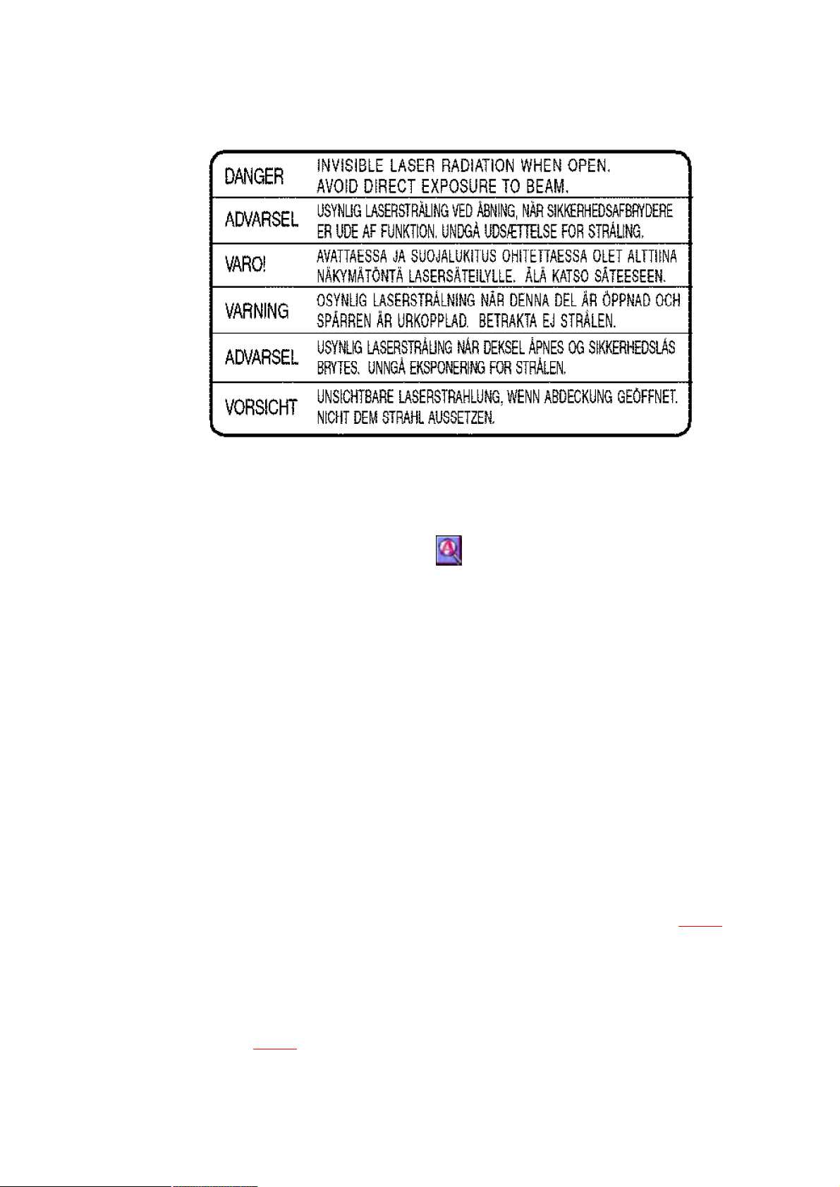
2. Precaution of Laser Diode
4
Page 5
3. Operating Instructions
4. Handling Precautions for Traverse Deck
The laser diode in the traverse deck (optical pickup) may break down due to
potential difference caused by static electricity of clothes or human body.
So, be careful of electrostatic breakdown during repair of the traverse deck
(optical pickup).
4.1. Handling the traverse deck (optical pickup)
1. The traverse deck (optical pickup) is an extremely high-precision construction
and must not be subjected to impact, excessive vibration, or other types of
rough handling.
2. In order to prevent static electricity damage to the laser diode, use a short pin
or similar tool to short the optical pickup’s flexible circuit boards after they
have been disconnected from the main circuit board. (as shown in Fig. 1 )
3. Handle the flexible circuit boards with care; excessive force could cause
them to be broken.
4. Do not turn the pre-set variable resistor (for adjustment of the laser power); it
has been adjusted at the factory.
(as shown in Fig. 2 )
5
Page 6
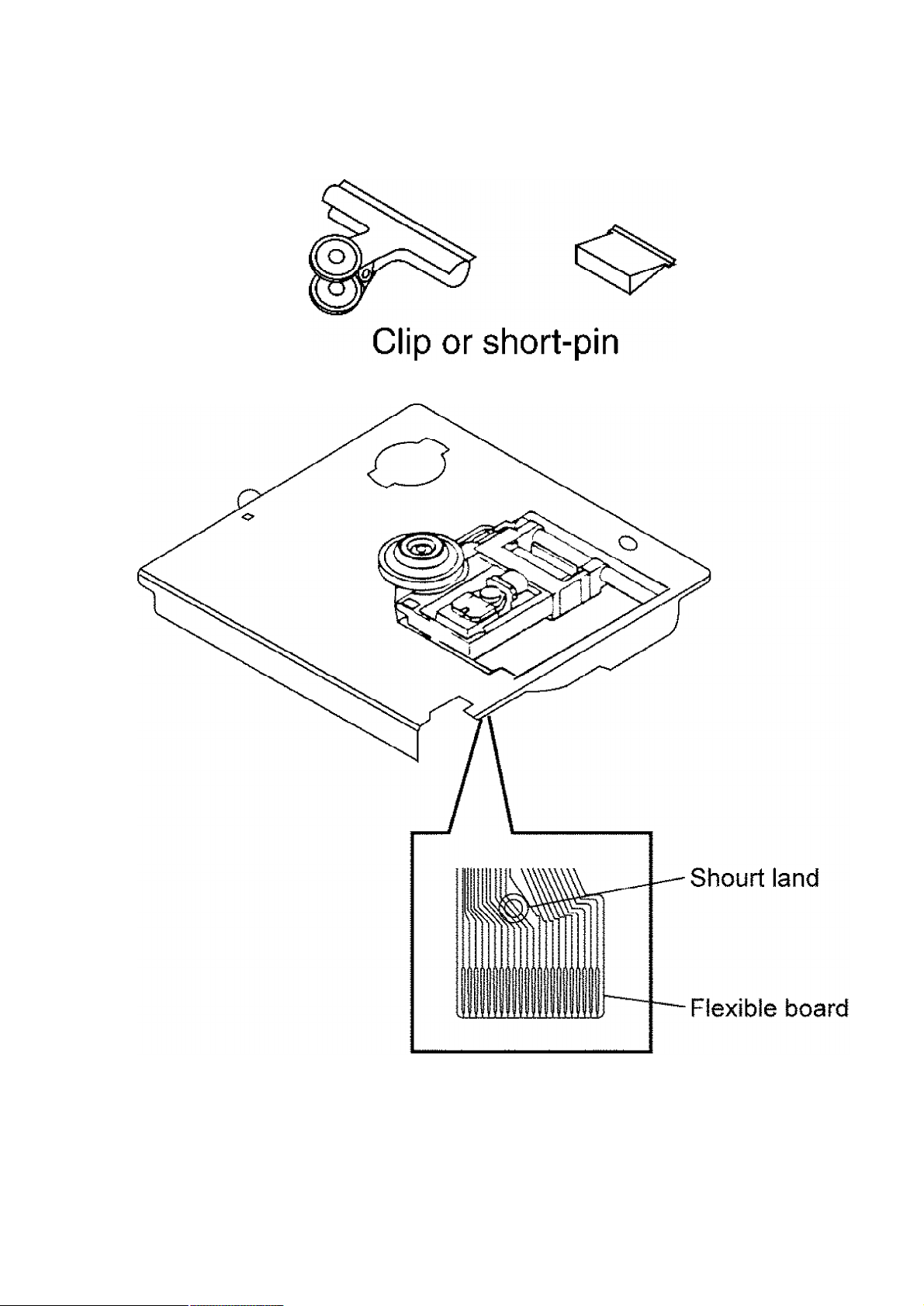
Fig. 1
Fig. 2
4.2. Grounding for electrostatic breakdown prevention
1. Human body grounding
6
Page 7
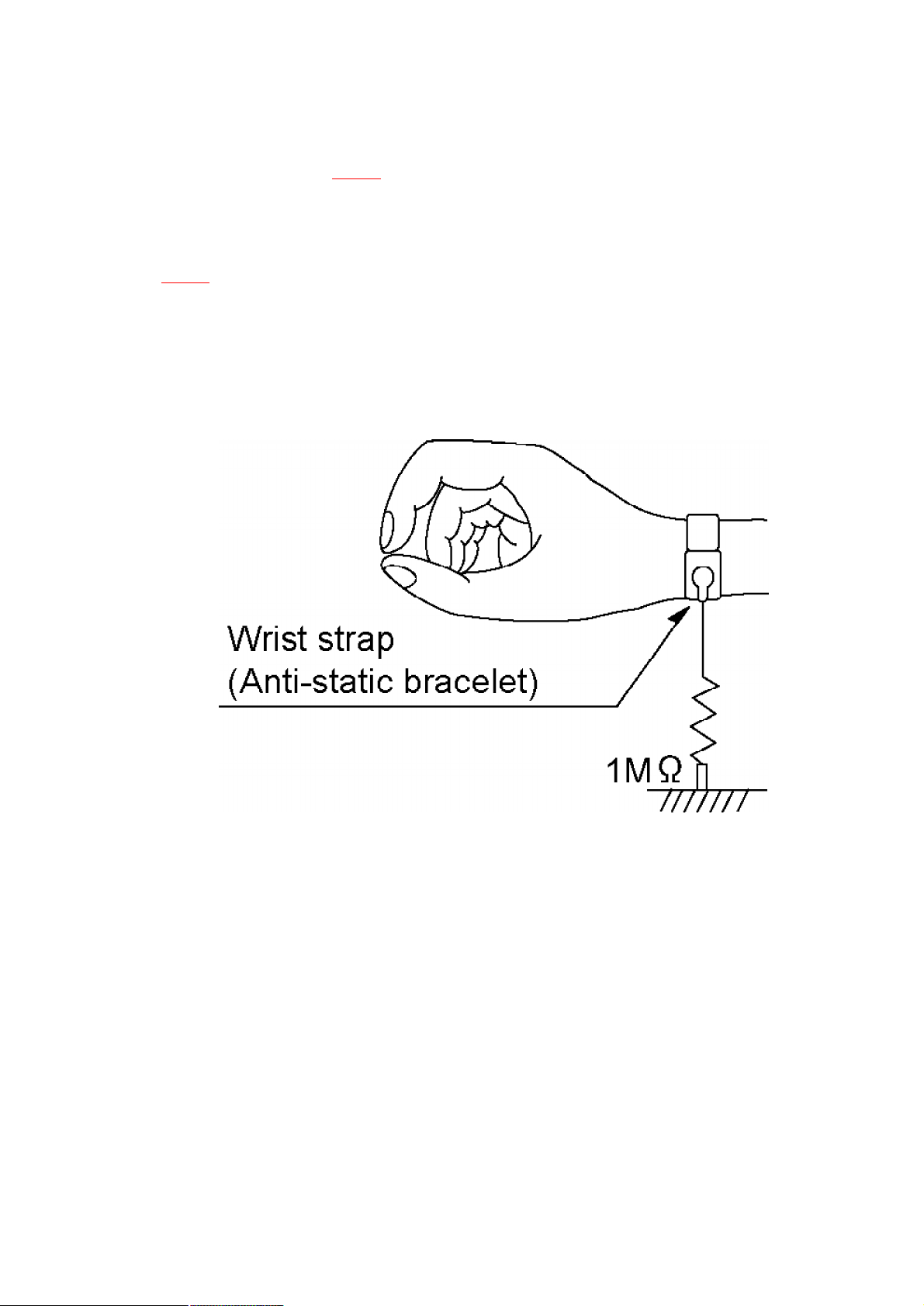
Use the anti-static wrist strap to discharge the static electricity from your
body. (as shown in Fig. 3 )
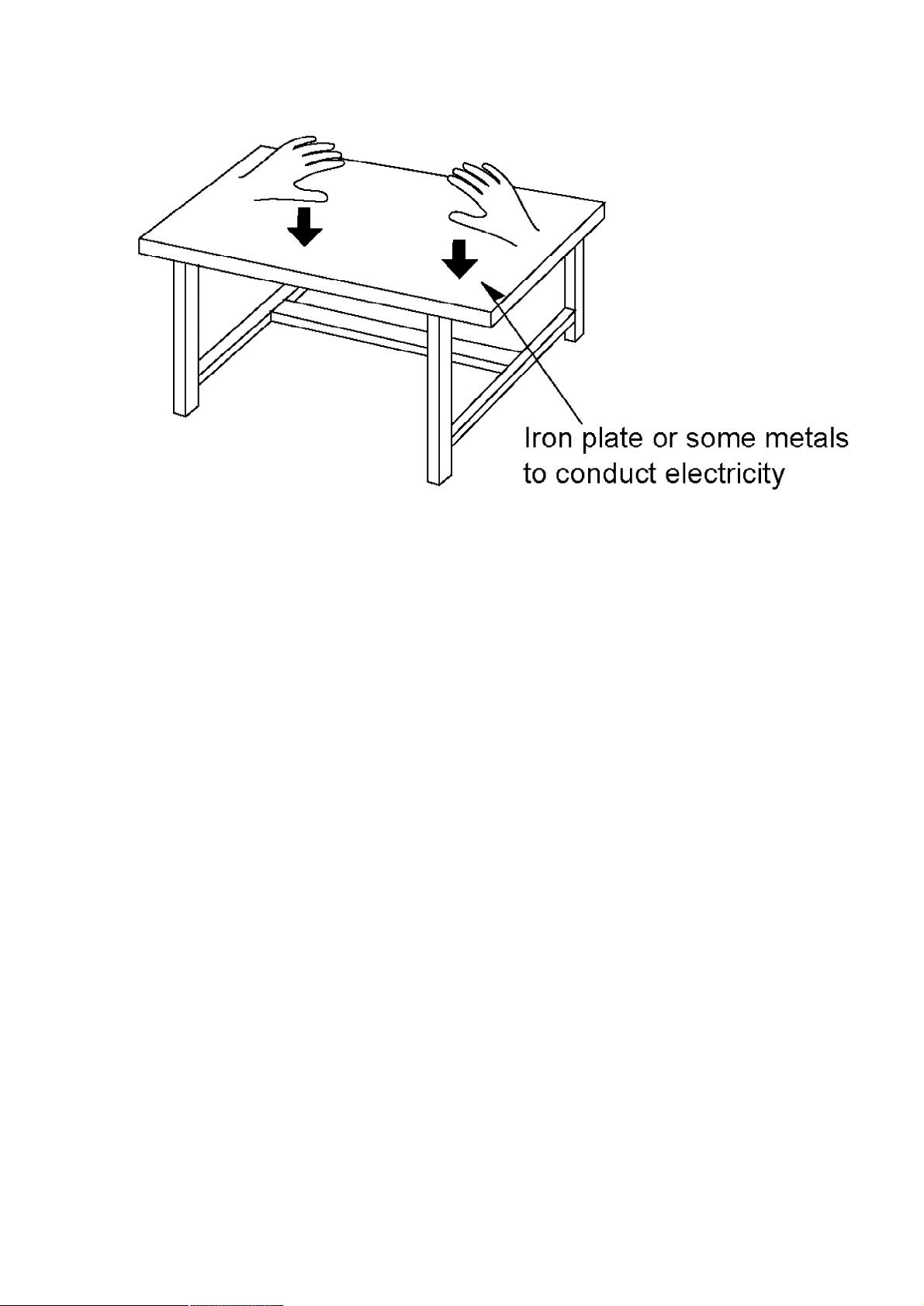
2. Work table grounding
Put a conductive material (sheet) or steel sheet on the area where the
traverse deck (optical pickup) is placed, and ground the sheet. (as shown in
Fig. 4 )
Caution
The static electricity of your clothes will not be grounded through the wrist
strap.
So, take care not to let your clothes touch the traverse deck (optical pickup).
Fig. 3
Fig. 4
7
Page 8
5. Operation Checks and Component Replacement
Procedures
- This section describes procedures for checking the operation of the major
printed circuit boards and replacing the main components.
- For reassembly after operation checks or replacement, reverse the respective
procedures. Special reassembly procedures are described only when
required.
- After replacing the main components (optical pickup or traverse motor, etc.)
of mechanism unit block, change to the adjust mode, and then perform the
“ROM/RAM auto-adjustment”.
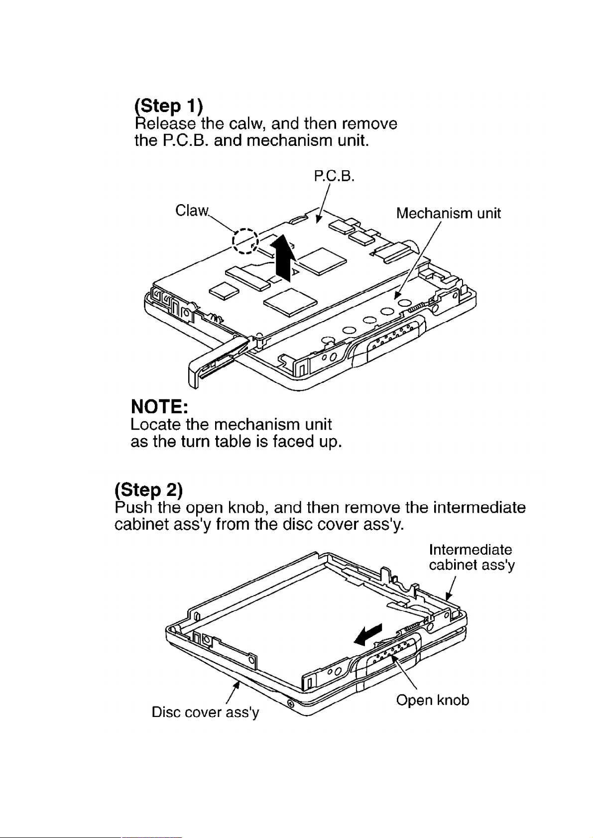
5.1. Checking for the P.C.B.
8
Page 9

9
Page 10
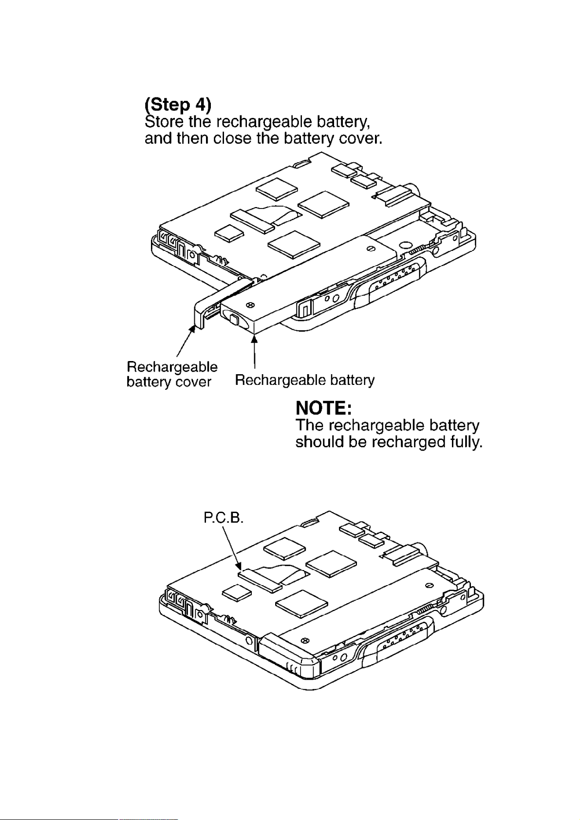
- Check the P.C.B. as shown below.
10
Page 11
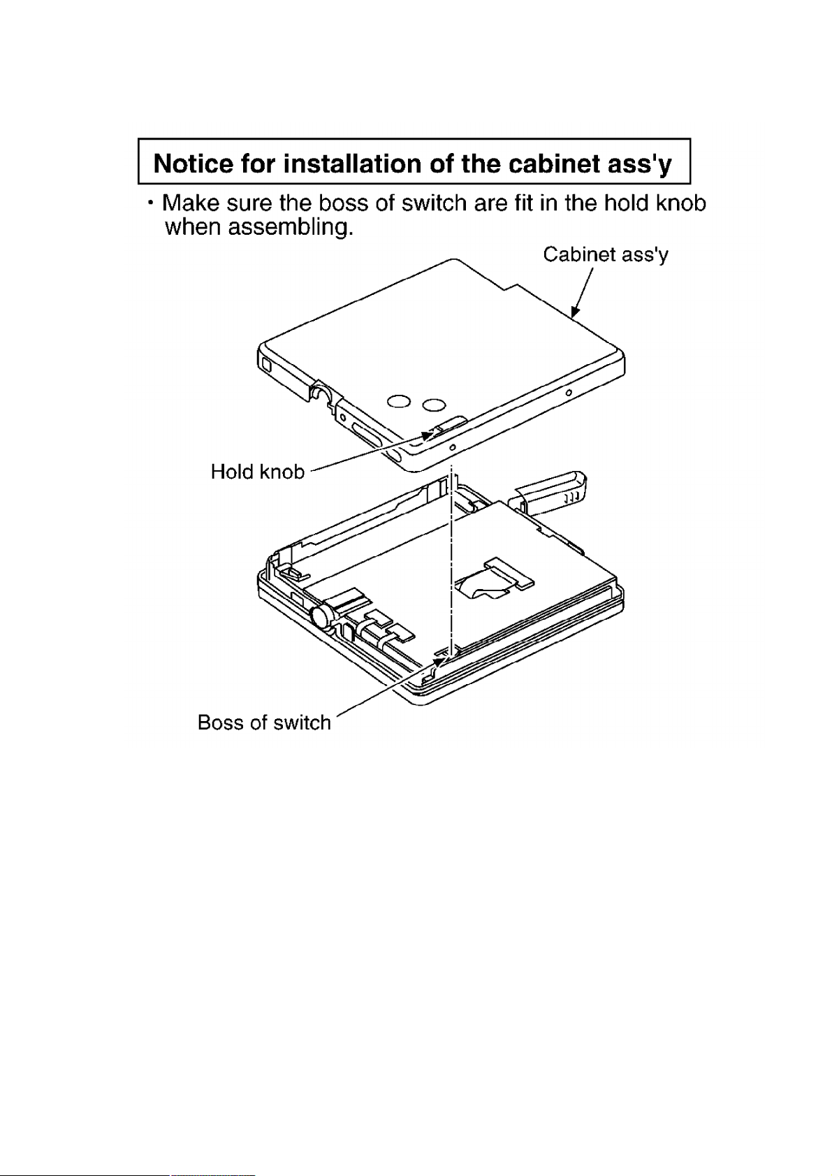
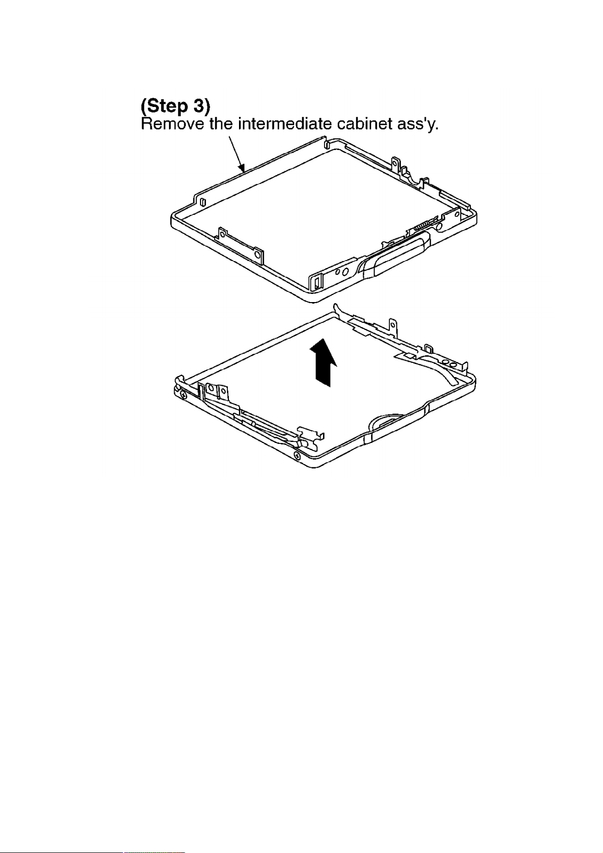
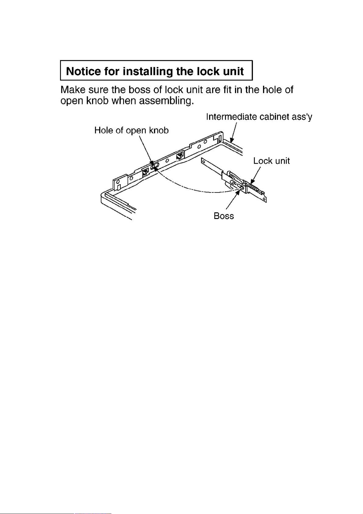
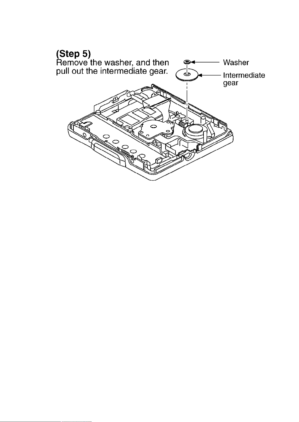
5.2. Replacement for the lock unit, open knob and
intermediate cabinet
- Follow the (Step 1) - (Step 3) of item 5.1.
111213
Page 12
Page 13
Page 14

14
Page 15
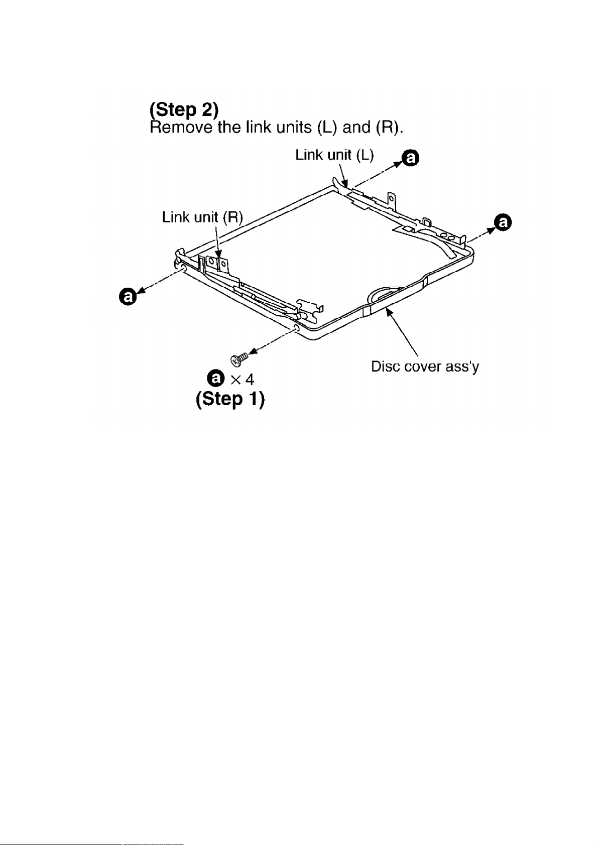
5.3. Replacement for the disc cover ass’y
- Follow the (Step 1) - (Step 3) of item 5.1.
- Follow the (Step 1) - (Step 3) of item 5.2.
15
Page 16
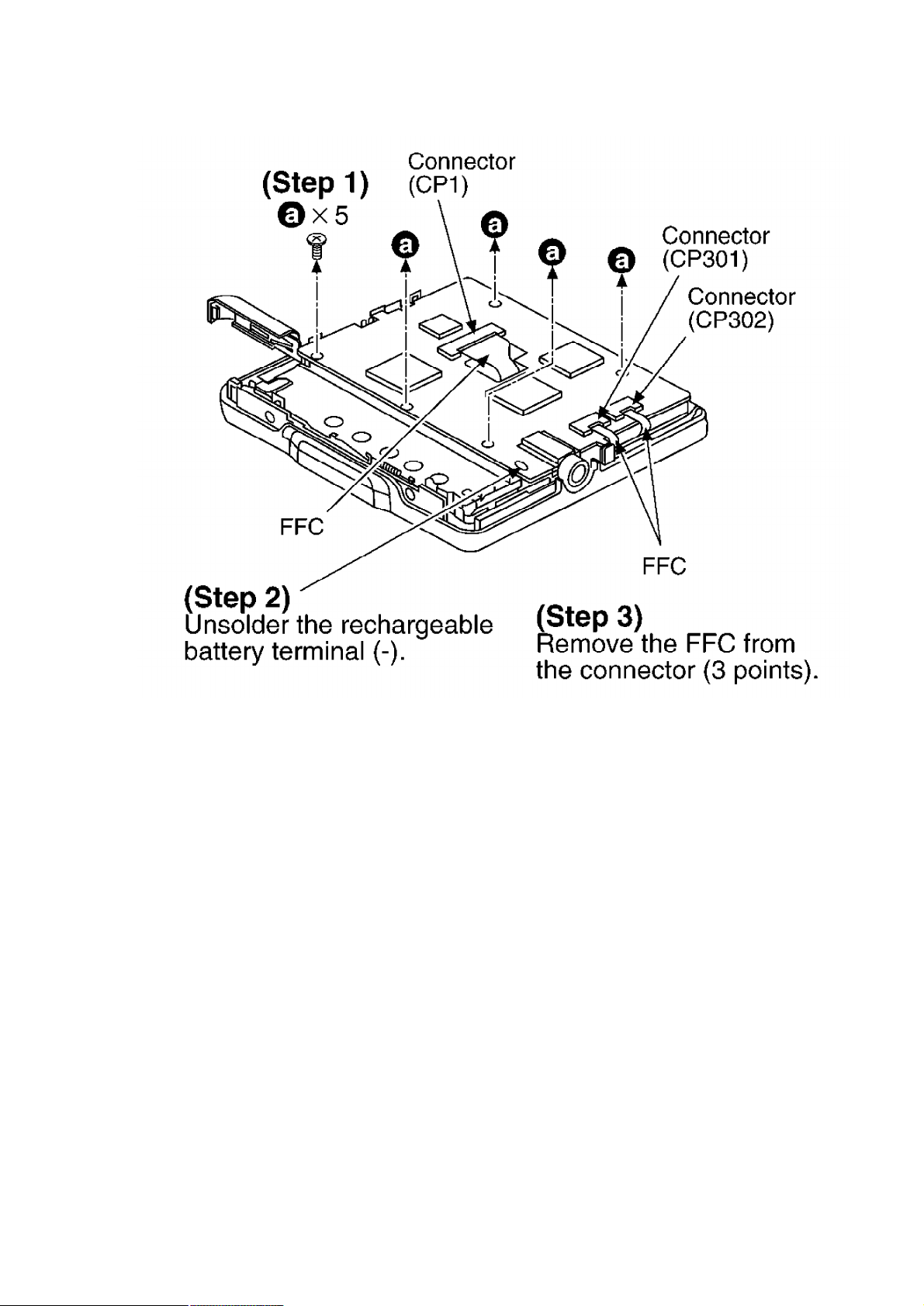
5.4. Replacement for the traverse motor
- Follow the (Step 1) - (Step 3) of item 5.1.
161718
Page 17
Page 18

Page 19
19
Page 20

5.5. Replacement for the optical pickup
- Follow the (Step 1) - (Step 3) of item 5.1.
- Follow the (Step 1) - (Step 5) of item 5.4.
2021222324
Page 21

Page 22

Page 23

Page 24

Page 25

6. Measurements and Adjustments
Note:
After replacing the main components (optical pickup or traverse motor, etc.) of
mechanism unit block, change to the adjust mode, and then perform the “Laser
power adjustment”, “Off-set automatic adjustment” and “Playback-onlydisc/
magneto-optical disc automatic adjustment”.
6.1. Instruments to prepare
1. Playback-only disc (Test disc RFKV0006)
2. Commercially available recordable disc (fully recorded with music) (magnetooptical disc)
25
Page 26

3. Laser power meter (LE8010 or compatible meter)
4. Remote controller
6.2. Laser power adjustment, Off-set automatic adjustment,
Playback-only disc/magneto-optical disc automatic
adjustment magnet
6.2.1. Enter the adjustment mode
Caution:
Place the unit on the insulation sheet with the disc cover side facing up.
1. Disassemble the unit so that only the mechanism unit and the printed circuit
board are exposed.
(Refer to (Step1) of the main part replacement procedure “5.2. Replacement
for the intermediate cabinet”).
2. Move the optical pickup to the innermost side and attach the disc cover.
3. Set the battery and connect the remote controller.
4. Turn off the power, and switch main unit’s HOLD switch off.
5. Press the VOL+, VOL-, , and keys on the remote controller within
two seconds. (as shown in Fig. 5 )
Fig. 5
6. When the adjustment mode is activated, “T0E ” will be displayed on the LCD
of remote controller. After “T0E ” is displayed, select the desired adjustment
item with the button or button of the remote controller. (If it is not
displayed, perform the procedures written above again.)
26
Page 27

Adjustment mode Display
Laser power adjustment T0E
Off-set automatic adjustment T1E
Magneto-optical disc automatic adjustment T2E
Playback-only disc automatic adjustment T3E
Jitter meajurement (74minutes) T4E
Jitter meajurement (60 minutes) T5E
Destination change T6E
Off-set automatic adjustment value check T7E
Magneto-optical disc automatic adjustment
value check
Playback-only disc automatic adjustment value
check
Error rate measurement (double velocity) TAE
ROM collection TBE
DRAM check TCE
Aging TDE
Tilt measurement TEE
PWB inspection TFE
T8E
T9E
*In the display of T0E ~ TFE shown above, you must adjust T0E , T1E , T2E and
T3E . You must perform the adjustment by observing the order T0E T1E T2E
T3E .
6.2.2. Laser Power Adjustment
Adjust each laser power: read power for reading (play).
6.2.2.1. Set the Unit to the Adjustment Mode
Cautions
About handling the optical pickup and the magnetic head.
- The optical pickup is structured precisely; therefore, it is very fragile. Be
careful not to touch it with the edge of the laser power meter. Do not touch
the lens.
- The sensor of the laser power meter is a very fine part. Be careful not to touch
it to the optical pickup lens.
- The focus point of the laser reaches to 356°F. Therefore, avoid adjusting
using laser power for a long time because the sensor of the laser power
meter may be burned.
- Do not set the unit to the laser power adjustment mode with the MD loaded.
Doing so may result in damage to the MD.
27
Page 28

- Laser diode in the optical pickup may be destroyed by the static electricity
generated in your clothes or body. Be especially careful with the static
electricity.
6.2.2.2. Adjustment Procedure
1. Uncover the laser power meter. (as shown in Fig. 6 )
Fig. 6
2. Locate the sensor of the laser power meter at a position above the optical
pickup (horizontally at a level of the disc position). (as shown in Fig. 7 )
Fig. 7
3. Press the key of the remote controller (“T0E ” changes to “LD ” of the
LCD).
28
Page 29

4. Press the key of the remote controller (“LD ” changes to “LP ” of the
LCD).
5. Set the laser power at 600 W±10% by using VOL+ and VOL- key of the
remote controller.
[Specified range: 600 W±10%]
Caution:
Proceeding on to the subsequent adjustment procedure with the read power
exceeding 600 W±10% will result in damage to the optical pickup.
6. Set the laser power with the key of the remote controller (“LP ” changes
to “LDOK ” in the LCD).
7. Press the key of the remote controller (“LDOK ” changes to “T0E ” on
the LDC.
8. Remove the laser power meter. Laser power adjustment is finished.
[REFERENCE]
<For use of MD cartridge type laser power meter>
We recommend you to use a sensor type laser power meter for laser power
adjustment of this set.
But if available is a MD cartridge type only, follow the procedure below.
1. Disassemble the unit so that only the mechanism unit and the printed circuit
board are exposed. (as shown in Fig. 8 )
2. Set the laser power meter cartridge. (as shown in Fig. 8 )
3. Set the battery and attach and secure the battery cover with a rubber band.
(as shown in Fig. 9 )
4. Follow the steps for “6.2.1. Enter the adjustment mode”. (Subsequent
procedures are the same as those for the sensor type.)
Fig. 8
29
Page 30

Fig. 9
30
Page 31

6.2.3. Off-set automatic adjustment
1. Remove the mechanism unit from the disc cover. Then move the optical
pickup to the center, and attach the mechanism unit again to the disc cover.
2. With “T1E ” displayed, leave the disc cover open.
3. Pressing the key on the remote controller will start adjustment.
4. During adjustment, “FADJ ” is displayed on the LCD of the remote controller.
If there is no abnormality, “FADJOK ” will be displayed.
5. Pressing the key while “FADJOK ” is displayed will return to the “T1E ”
display mode.
6.2.4. Magneto-optical disc automatically adjustment
1. Have “T2E ” indicated on display, and set the full-recorded magneto-optical
disc. (Check to make sure the disc is properly seated.)
2. Press key of the remote controller. The adjustment is started.
3. During adjustment, “AADJ ” is displayed on the LCD of the remote controller.
If there is no abnormality, “AOK ” will be displayed.
Note:
If it is displayed “ANG ”, check “7. Troubleshooting Guide” in the order.
31
Page 32

4. Press key (“AOK ” or “ANG ” changes to “T2E ”).
5. After the adjustment is finished, remove the disc.
6.2.5. Playback-only disc automatic adjustment
1. Have “T3E ” indicated on display, set the playback-only disc.
(Check to make sure the disc is properly seated.)
2. Press key of the remote controller. The adjustment is started.
3. During adjustment. “AADJ ” is displayed on the LCD of the remote controller.
If there is no abnormality, “AOK ” will be displayed.
Note:
If it is displayed “ONG ”, check “7. Troubleshooting Guide” in the order.
4. Press key (“OOK ” or “ONG ” changes to “T3E ”).
5. After the adjustment is finished, remove the disc.
6.2.6. How to get out the adjustment mode
Remove the battery when you finish the adjustment.
6.3. Checking the main unit's keys
1. Set the battery and connect the remote controller.
2. Turn off the power, and switch main unit’s HOLD switch OFF.
3. Press the VOL+, VOL-, , and keys on the remote controller within
two seconds. (as shown in Fig. 5 )
4. When the unit enters the unit key check mode, the display shows “T KEX ”.
While “T KEX ” is displayed, press the , , and VOL(+, -) keys
of the unit in the specified order and then switch off the HOLD switch.
*When thefirst key is pressed, the display will change to “T ”.
32
Page 33

Main unit’s keys LCD display position and letters
After the third key is pressed, the second digit displayed
will change from “ ” to “O ”.
VOL+ After the second key is pressed, the third digit displayed
VOL-
HOLD OFF The first digit displayed will change from “ ” to “O ”.
will change from “ ” to “O ”.
5. After all keys have been pressed and there is no abnormality, “T OOO ” will
be displayed.
6. Perform below voltage check about the keys come under if it is not displayed
“T OOO ”.
Main unit’s keys Check points ON OFF
HOLD TP428 0V 2.2V
IC201 48pin 0V 2.2V
TP421 1.13V 2.2V
TP421 1.69V 2.2V
VOL+ TP421 0V 2.2V
VOL- TP421 0.58V 2.2V
Note:
Refer to “10. Printed Circuit Board Diagram” for the test points.
7. Remove the battery when you exit from this mode.
7. Troubleshooting Guide
33343536373839
Page 34

Page 35

Page 36

Page 37

Page 38

Page 39

Page 40

40
Page 41

8. Schematic Diagram Notes
8.1. Type Illustration of IC's, Transistors and Diodes
41
Page 42

8.2. Schematic Diagram Notes
This schematic diagram may be modified at any time with the development of
new technology.
Notes:
S201
S202
S203
S204
S206
S207
S208
Volume control switch (+)
:
volume control switch (-)
:
:
Skip/search switch ( )
:
Skip/search switch ( )
:
Play/stop switch ( )
Cover open/close det. switch
:
Hold switch in “OFF” position. (HOLD)
:
- Indicated voltage values are the standard values for the unit measured by the
DC electronic circuit tester (high-impedance) with the chassis taken as
standard. Therefore, there may exist some errors in the voltage values,
depending on theinternal impedance of the DC circuit tester.
No mark: MD STOP
( ): MD play [1kHz, L+R, 0dB]
Important safety notice:
Components identified by mark have special characteristics important for
safety.
Furthermore, special parts which have purpose of fire-retardant (resistors), highquality sound (capacitors), low-noise (resistors), etc. are used. When replacing
any of components, be sure to use only manufacture's specified parts shown in
theparts list.
Caution!
IC and LSI are sensitive to static electricity.
Secondary trouble can be prevented by taking care during repair.
Cover the parts boxes made of plastics with aluminum foil.
Ground the soldering iron.
Put a conductive mat on the work table.
Do not touch the legs of IC or LSI with the fingers directly.
42
Page 43

Voltage and signal line
: Positive voltage line
: Playback signal line
9. Schematic Diagram
10. Printed Circuit Board Diagram
11. Block Diagram
12. Terminal Function of IC's
12.1. IC1 (AN86772FHKEBV): RF AMP
43
Page 44

Pin
No.
Mark I/O
Division
Function
1 LDO O LD amp. output terminal
2 LDIN I LD amp. reverse input
terminal
3 APCPD I Photo diode light quantity
det. input terminal
4 NC — Not used, open
5 ARFO O RF amp. output terminal
6 NC — Not used, open
7 EQIN I EQ input terminal
8 CRFAGC I RFAGC capacitor
connection terminal
(Connected to power
supply through capacitor)
9 OUTRF O EFM output terminal
10 NC — Not used, open
11 PEAK O EFM bright-side detection
output terminal
12 GND — GND terminal
13 BOTM O EFM dark-side detection
output terminal
14 CEA I 3T envelope det. capacitor
connection terminal
(Connected to power
supply through capacitor)
15 MON3T O 3T envelope output
terminal
16 CC O C signal’s dark-side
detection/amplified output
terminal
17 DD O D signal’s dark-side
detection/amplified output
terminal
18 V
CC
I Power supply terminal
19 BB O B signal IV conversion
output terminal
20 AA O A signal IV conversion
output terminal
21 FE2 O F2 signal IV conversion
output terminal
22 FE1 O F signal IV conversion
output terminal
23 NC — Not used, open
44
Page 45

24
Pin
No.
25 ADIP O ADIP signal output terminal
26 NC — Not used, open
27
28 RFSWHL I Reflectance H/L switching
29 RFSWPG I Pit/Crv switching signal
30 GND2 — GND terminal
31 NC — Not used, open
32 MONI
33 BPF I ADIP BPF switching signal
34 LD ON I APC circuit control signal
35
36 NC — Not used, open
37
38 F1 I F1 signal input terminal
39 F2 I F2 signal input terminal
40 A I A signal input terminal
41 B I B signal input terminal
42 VREF O Reference signal output
43 RF2 I RF2 signal input terminal
44 RF1 I RF1 signal input terminal
45 CENVD — D signal detection
46 CENVC — C signal detection
47 D I D signal input terminal
48 C I C signal input terminal
Mark I/O
OFF
NRFSTBY
Function
Division
signal input terminal
input terminal
I 3T MON circuit control
signal input terminal
input terminal
input terminal
I Standby control signal
input terminal
terminal
capacitor connection
terminal (Not used, open)
capacitor connection
terminal (Not used, open)
12.2. IC101 (MN66620RF): ATRAC ENCORDER/DECORDER,
SERVO SIGNAL PROCESSOR
45
Page 46

Pin
No.
Mark I/O
Division
Function
1 RVDD 3 I Power supply to internal
DRAM
2 RVDD 18 O Voltage regulator output
terminal (Connects to
internal DRAM supply
terminal)
3 RVDD 23 — Voltage regulator input
terminal (Accepts a supply
voltage identical to that for
IO pad)
4 LON I Voltage regulator ON/OFF
control signal input
terminal (1:ON, 2:OFF)
5 TMDISY O Microprocessor interrupt
signal 3 output terminal
(for monitoring)
6 TSGSY NCO ATRAC frame sync. signal
output terminal (for
monitoring)
7 MONI6 O Monitor signal output
terminal 6
8 MONI5 O Monitor signal output
terminal 5
9 NRST I Chip Reset signal input
terminal (O:reset)
10 SELAD I Microprocessor IF address
data select signal input
terminal
11 SSCK I Microprocessor IF shift
clock signal input terminal
12 SSDW I Microprocessor IF write
data input terminal
13 SSDR O Microprocessor IF read
data output terminal
14 NRQ O Microprocessor interrupt
signal 1 output terminal
15 MDAS
CSY
O Microprocessor interrupt
signal 2 output terminal
16 FG I FG input terminal
17 TRDP O Tracking drive (+) PWM
signal output terminal
18 TRDM O Tracking drive (-) PWM
signal output terminal
46
Page 47

Pin
No.
Mark I/O
Division
Function
19 RVDD 1 I Power supply to internal
DRAM
20 RVSS 2 — GND to internal DRAM
21 FODP O Focus drive (+) PWM signal
output terminal
22 FODM O Focus drive (-) PWM signal
output terminal
23 SPDP O Spindle drive (+) PWM
signal output terminal
24 SPDM O Spindle drive (-) PWM
signal output terminal
25 LDON O Laser power control output
terminal (1:ON, 0:OFF)
26 PVPP
DRAM1
— Monitor to internal DRAM
output terminal (Not used,
open)
27 IVDD 0 — Power supply terminal for I/
O pad
28 DVDD 0 — Digital power supply
29 XI I Crystal oscillator input
terminal (F=16.9344MHz)
30 DVSS 0 — Digital GND
31 XO O Crystal oscillator output
terminal (F=16.9344MHz)
32~34STP10~STP12
I Stepping motor status
input terminal (0~2)
35~37STP00~STP02
O Stepping motor drive
signal output terminal (0~2)
38 RFSWHL O Laser power control output
terminal (PIT/GRUVE
switching)
39 RFSWPG O Laser power control output
terminal (Reflectance
switching)
40 PEFMS I EFM signal input terminal
41
EFMPLLF
O EFM PLL filter output
terminal
42 PEFM1 O Loop filter terminal for
EFM data slicing (Not
used, open)
43 EFMFIL O Input filter switching for
EFM data slicing terminal
44 EFMIREF I Reference current setting
terminal for EFM PLL
47
Page 48

terminal
for
EFM
PLL
Pin
No.
Mark I/O
Division
Function
45 ADIP I ADIP signal input terminal
46 PEAK I Servo ADC input terminal
47 BTOM
48 BAT
49 GAIRAN
50 MON3T
51 VREFI I Servo ADC input/voltage
reference for ADIP
comparator
52 FF2 I Servo ADC input terminal
53 AVDD 0 — Analog power supply
54 FF1 I Servo ADC input terminal
55 AVSS 0 — Analog GND
56 DD I Servo ADC input terminal
57 CC
58 BB
59 AA
60 AVDD 1 — Analog power supply
61 AVSS 1 — Analog GND
62 AVSS 2
63 ADACL O Audio output terminal (L-
ch.)
64 ADACR O Audio output terminal (R-
ch.)
65 AVDD 3 — Analog power supply
(dedicated to audio DAC)
66 DVDD 1 — Digital power supply
67 DVSS 1 — Digital GND
68 SEL0 I Connected to GND
69 RVDD 2 I Power supply to internal
DRAM
70 RVSS 3 — GND to internal DRAM
71 SEL1 I Connected to GND
72, 73TS1, TS2
74~78
MONI4
~MONI0
O Monitor signal output
terminal (4~0)
79 TS3 I Connected to GND
80 TSCTSY O Microprocessor interrupt
signal 4 output terminal
(for Monitor)
48
Page 49

12.3. IC201 (MN101C32GAE): SYSTEM CONTROL
Pin
No.
10 VREF+ — AD reference input (+)
11 V
12 OSC2 O System clock output
13 OSC1 I System clock input
14 V
15 XI — Sub clock input terminal
16 XO — Sub clock output terminal
17 MMOD — Memory mode switching
18 REM
19 LINK
20 — — Not used, open
21 SSDW O Write data output terminal
Mark I/O
Division
1 VREF- — AD reference input (-)
(connected to GND)
2 (AN0)
REM
KEY
3 (AN1)
KEY IN
4 (AN2)
BATT
5 (AN3) — Not used, connected to
6 (AN4)
7 (AN5)
8 (AN6)
9 (AN7) — Not used, connected to
DD
SS
DATA
RXD
I Remote cont. key input
terminal
I Unit key input terminal
I Battery voltage det. input
terminal
GND
power supply terminal
(connected to power
supply)
— Power supply terminal
terminal (F=6MHz)
terminal (F=6MHz)
— GND terminal
(Not used, connected to
GND)
(Not used, open)
input terminal (Not used,
connected to GND)
O LCD driver data output
terminal
I Link serial communication
RXD input terminal
for CPU interface
Function
49
Page 50

Pin
No.
Mark I/O
Division
Function
22 SSDR I Read data input terminal
for CPU interface
23 SSCLK O Clock output terminal for
CPU interface
24 BUZZER O Confirmation tone output
terminal
25 RST I Reset signal input terminal
26 CFSYNC I Synchronize signal input
terminal for CPU interface
27 SELAD O Address select output
terminal for CPU interface
28 — — Not used, open
29 MDISY I Reader synchronize signal
input terminal
30 LD PWM O Laser power controlling
PWM output terminal
31 DCIN
WAKEUP
I Charger wakeup detection
signal input terminal
32 NRQ I Microprocessor service
request input terminal
33
MDASCSY
I MDA service selector
signal input terminal
34 OPEN
SW
I Lid open detection input
terminal (H:Open)
35 SCTSY I ADIP synchronize signal
input terminal
36~42
43
— — Not used, open
CHARGE1
O Recharging control output
terminal
44~46
— — Not used, open
47 HOLD I HOLD SW input terminal (L:
HOLD)
48 PLAY
KEY
49 REM
KEY
WAKEUP
50
DOCTOR
I PLAY PAUSE KEY input/
wake up input terminal
I REM KEY input/micro
computer wake up input
terminal
I Process inspection mode
input terminal (L:Process
inspection) (pulled up to V
via resistor)
DD
50
Page 51

Pin
No.
51 BATT
Mark I/O
Division
— Battery check LED drive
CHK
LED
Function
output terminal (Not used,
open)
52 JITTER OK— Process inspection output
terminal (Not used, open)
53 REG2 I Model switching input
terminal (L:MJ88, H:MJ80)
54 REG3 I Recharge switching input
terminal
55,
— — Not used, open
56
57 EEP CS O EEP ROM chip select
output terminal
58 EEP CK O EEP ROM clock output
terminal
59 EEP
DATA O
60 EEP
DATA I
61~64
— — Not used, open
O EEP RAM DATA output
terminal
I EEP ROM DATA input
terminal
65 MUTE A O Analog mute A output
terminal
66 MUTE B O Analog mute B output
terminal
67 NRF
STBY
68 DRAM
O RF AMP standby output
terminal
I DRAM check input terminal
CHK
69,
— — Not used, open
70
71 MONI
OFF
O RF monitor control output
terminal (H:OFF, L:ON)
72 BPF O RF band pass filter control
output terminal (L:WIDE)
73 RF
CONT
74 MUTE
MODE
O RF power supply control
output terminal
— Mute mode switching input
terminal (Connected to
GND)
75 POWER
CNT
O Power supply control
output terminal
76 ELON I EL display control input
terminal (L:ON)
51
Page 52

Pin
No.
77 PC O 4-ch. driver standby output
78 STBY2 O FD/TR coil power supply
79
80 MSP
Mark I/O
BATTCHK
RST
Function
Division
terminal (L:Standby)
control output terminal
O Battery check output
terminal (Not used, open)
O MSP reset output terminal
(L:Reset)
12.4. IC301 (C0GBZ000006): FOCUS/TRACKING COIL/
TRAVERSE MOTOR DRIVE/ROTALY DETECTOR
52
Page 53

Pin
No.
Mark I/O
Division
Function
1 IN1R I H bridge 1 reverse input
terminal
2 IN2F I H bridge 2 forward input
terminal
3 IN2R I H bridge 2 reverse input
terminal
4 STALL I Standby input terminal
5 STHB I H1, H2 bridge mute input
terminal
6 SPVM1 I Spindle power unit’s power
supply 1
7 SPUOUT O Spindle motor coil (U)
output terminal
8 SPPG1 — Spindle power unit’s GND1
9 NC — Not used, open
10 SPVOUT O Spindle motor coil (V)
output terminal
11 SPVM2 I Spindle power unit’s power
supply 2
12 SPWOUT O Spindle motor coil (W)
output terminal
13 SPPG2 — Spindle power unit’s GND2
14 PWVM I Half bridge power unit’s
power supply
15 PWOUT O Half bridge output terminal
16 PWPG — Half bridge power unit’s
GND
17 PWIN1 I Half bridge1 input terminal
53
Page 54

Pin
No.
Mark I/O
Division
Function
18 SPUIN I SPIN detection comparator
(U-phase) input terminal
19 SPVIN I SPIN detection comparator
(V-phase) input terminal
20 SPWIN I SPIN detection comparator
(W-phase) input terminal
21 SPCOM I SPIN motor coil neutral
point input terminal
22 RIB I Soft switching gain control
resistor terminal
23 CST I Startup oscillation
capacitor terminal
24 CSL1 I Slope capacitor connection
terminal 1
25 CSL2 I Slope capacitor connection
terminal 2
26 FG O FG output terminal
27 BRK+ I Brake comparator (+) input
terminal
28 BRK- I Brake comparator (-) input
terminal
29 ASGND — Small signal block GND
(Bip.)
30 SGND — Small signal block GND
(MOS)
31 S1 I Stepping decorder 1 input
terminal
32 S2 I Stepping decorder 2 input
terminal
33 S3 I Stepping decorder 3 input
terminal
34 BEMFU O Step detect comparator (U)
output terminal
35 BEMFV O Step detect comparator (V)
output terminal
36 BEMFW O Step detect comparator (W)
output terminal
37 SLCOM I Step motor coil center
input terminal
38 SLPG2 — Stepping power unit’s GND
2
39 SLWOUT O Stepping motor (W) output
terminal
54
Page 55

Pin
No.
Mark I/O
Division
Function
40 SLVM2 I Stepping power unit’s
power supply 2
41 SLVOUT O Stepping motor (V) output
terminal
42 SLPG1 — Stepping power unit’s GND
1
43 SLUOUT O Stepping motor (U) output
terminal
44 SLVM1 I Stepping power unit’s
power supply 1
45 VCC 2 — Small signal block power
supply terminal 2 (Bip.)
46 VCC 1 — Small signal block power
supply terminal (MOS)
47 VG O Charge pump output
terminal
48 C2M — Charge pump capacitor 2
terminal (-)
49 C2P — Charge pump capacitor 2
terminal (+)
50 CIM — Charge pump capacitor 1
terminal (-)
51 CIP — Charge pump capacitor 1
terminal (+)
52 EXTCLK — Synchronize clock input
terminal (Not used, open)
53 NC — Not used, open
54 H2PG2 — H bridge 2 power unit’s
GND 2
55 H2ROUT O H bridge 2 reverse output
terminal
56 H2VM I H bridge 2 power unit’s
power supply
57 H2FOUT O H bridge 2 forward output
terminal
58 H2PG1 — H bridge 2 power unit’s
GND 1
59 H1PG2 — H bridge 1 power unit’s
GND 2
60 H1ROUT O H bridge 1 reverse output
terminal
61 H1VM I H bridge 1 power unit’s
power supply
55
Page 56

Pin
No.
62 H1FOUT O H bridge 1 forward output
63 H1PG1 — H bridge 1 power unit’s
64 IN1F I H bridge 1 forward input
Mark I/O
Division
Function
terminal
GND 1
terminal
13. Caution in Use of Rechargeable Battery Ass'y
- Take Rechargeable Battery Ass’y out of Battery Carrying Case and use it.
- Be sure to carry Rechargeable Battery Carrying Case. If not, it may either heat
or ignite by shorting with a metal. (as shown in Fig. 10 )
Fig. 10
14. Supply of Rechargeable Battery Ass'y as
Replacement Parts
Please take note of the following points relating to Battery Carrying Case to be
used for protection of Rechargeable Battery Ass’y from shorting. Replacement
Parts:
- Rechargeable Battery Ass’y (RP-BP62EYS1) supplied will be provided with
Battery Carrying Case (RFA0475-Q).
- No replacement parts will be supplied for Rechargeable Battery Ass’y without
Battery Carrying Case.
56
Page 57

- Replacement parts will be supplied for Battery Carrying Case (RFA0475-Q)
without Rechargeable Battery Ass’y.
- To your customers, delivery Rechargeable Battery Ass’y together with Battery
Carrying Case to prevent shorting accidents that may occur when
Rechargeable Battery Ass’y is carried about Battery Carrying Case. (as shown
in Fig. 11 )
Fig. 11
15. Replacement Parts List
Notes:
*Important safety notice:
Components identified by mark have special characteristics important for
57
Page 58

safety.
*Furthermore, special parts which have purposes of fire-retardant (resistors),
high-quality sound (capacitors), low-noise (resistors), etc. are used.
*When replacing any of components, be sure to use only manufacture’s
specified parts shown in the parts list.
*The parenthesized indications in the Remarks columns specify the areas.
(Refer to the cover page for area.)
*Warning: This product uses a laser diode. Refer to caution statements.
*ACHTUNG:Die lasereinheit nicht zerlegen.Die lasereinheit darf nur gegen einc
vom hersteller spezifizierte einheit ausgetauscht werden.
*Capacity values are in microfarads (uF) unless specified otherwise, P=Picofarads (pF) F=Farads (F)
*Resistance values are in ohms, unless specified otherwise, 1K=1,000 (OHM), 1M
=1,000K (OHM)
*The marking <RTL> indicates that the Retention Time is limited for this item.
After the discontinuation of this assembly in production, the item will continue
to be available for a specific period of time. The retentionperiod of availability is
dependant on the type of assembly, and in accordance with the laws governing
part and product retention. After the end of this period, the assembly will no
longer be available.
*"<IA>" mark in Remarks indicates languages of instruction manuals.
[<IA>:English/Spanish/French/German/Netherlands/Swedish/Italian/Danish]
Ref. No. Part No. Part Name & Description Pcs Remarks
1 RHD14088-S SCREW 4
2 RXQ0715-1 LINK UNIT(L) 1
3 RXQ0716-1 LINK UNIT(R) 1
4 RYF0563Z-S DISC COVER 1
5 RYQ0333-S INTERMEDIATE CABINET 1
5-1 RGV0267-S OPEN KNOB 1
6 RYK1039A-S CABINET ASS’Y 1
6-1 RGK1309-S JACK PIECE 1
6-2 RGU1916-S OPERATION BUTTON 1
6-3 RGU1917-S VOLUME BUTTON 1
6-4 RGV0268-S HOLD KNOB 1
7 RHD14076-S SCREW 6
8 RKK0141-S RECHARGEABLE BATT.COVER 1
9 RDG0477 INTERMEDIATE GEAR 1
10 RHD14078 SCREW 1
11 RHW11011 WASHER 1
12 RMC0392-2 SPRING 1
13 RXK0324 TRAVERSE UNIT 1
13-1 BRL1A1CWB TRAVERSE MOTOR 1
13-2 RHD14074 SCREW 1
13-3 RJC99038 RECHARGE.BATT.TERMINAL(-) 1
13-4 XQN14+B2FC SCREW 1
58
Page 59

Ref. No. Part No. Part Name & Description Pcs Remarks
13-5 RMX0156-1 STOPPER RUBBER 1
14 RJR0195-2 BATTERY SHAFT 1
15 RAF2000A-M OPTICAL PICKUP 1
16 RXJ0025 DRIVE SHAFT 1
17 RHD14067 SCREW 5
18 RJC99039 RECHARGE.BATT.TERMINAL(+) 1
A1 RP-BP62EYS1 RECHARGEABLE BATT.ASS’Y 1
A1-1 RFA0475-Q RECHARGEABLE BATT.CASE 1
A2 K3ZZ00200038 EXTERNAL BATTERY CASE 1
A3 RFC0056-K CARRING CASE 1
A4 RFEV025P-SM WIRED REMOTE CONTROL 1
A4-1 RYQ0312-W REMOCON.CLIP 1
A5 L0BAB0000162 STEREO EARPHONES 1
A6 RP-BC155AEBY CHARGER 1 (EB)
A6 RP-BC155AEYB CHARGER 1 (EG)
A7 RQT5683-B INSTRUCTION MANUAL 1 <IA>
A8 RQCB0169 SERVICE CENTER LIST 1
C5 RCST0GZ226RG 4V 22U 1 F3E0G226A002
C6 ECUVNJ105KBV 63V 1U 1 F1H0J105A002
C7,C8 ECUVNA224KBV 10V 0.22U 2 F1H1A224A028
C9 ECUVNJ474KBV 63V 0.47U 1 F1H0J474A002
C13 ECUENA104KBQ 10V 0.1U 1 F1G1A104A014
C14 ECUE1H102KBQ 50V 1000P 1 F1G1H102A457
C19 ECUENA104KBQ 10V 0.1U 1 F1G1A104A014
C20 RCST0GZ106RG 4V 10U 1 F3E0G106A002
C23 ECUENA104KBQ 10V 0.1U 1 F1G1A104A014
C24 ECUE1C103KBQ 16V 0.01U 1
C28 RCST0GZ106RG 4V 10U 1 F3E0G106A002
C65 ECUENH272KBQ 50V 2700P 1
C66 ECUENA823KBQ 10V 0.082U 1
C101 ECUE1C223KBQ 16V 0.022U 1 F1G1C223A044
C102 ECUE1C103KBQ 16V 0.01U 1
C103 ECUENA104KBQ 10V 0.1U 1 F1G1A104A014
C105 ECUVNA224KBV 10V 0.22U 1 F1H1A224A028
C106 ECUENA104KBQ 10V 0.1U 1 F1G1A104A014
C107 RCST0GZ106RG 4V 10U 1 F3E0G106A002
C110,11 ECUE1E682KBQ 25V 6800P 2
C114 ECUENA104KBQ 10V 0.1U 1 F1G1A104A014
C116 ECUE1C822KBQ 16V 8200P 1 F1G1C8220002
C117,18 ECUENA104KBQ 10V 0.1U 2 F1G1A104A014
C119 RCST0EX227RE 2.5V 220U 1 F3G0E2270001
C201 ECUE1C103KBQ 16V 0.01U 1
C202 ECUE1H101KBQ 50V 100P 1
C203 RCST0GZ106RG 4V 10U 1 F3E0G106A002
C204 ECUENA104KBQ 10V 0.1U 1 F1G1A104A014
C206 ECUE1H101KBQ 50V 100P 1
C210 ECUE1C103KBQ 16V 0.01U 1
C211 ECUVNJ474KBV 63V 0.47U 1 F1H0J474A002
C212 ECUE1C103KBQ 16V 0.01U 1
C303 RCST0GZ226RG 4V 22U 1 F3E0G226A002
C304-06 ECUENA104KBQ 10V 0.1U 3 F1G1A104A014
C307 RCST0GZ106RG 4V 10U 1 F3E0G106A002
59
Page 60

Ref. No. Part No. Part Name & Description Pcs Remarks
C308 ECUENA104KBQ 10V 0.1U 1 F1G1A104A014
C309-11 ECUENC333KBQ 16V 0.033U 3 F1G1C333A004
C318 ECUVNJ274KBV 63V 0.27U 1 F1H0J2740001
C319,20 ECUENA104KBQ 10V 0.1U 2 F1G1A104A014
C323-25 ECUE1H222KBQ 50V 2200P 3 F1G1H222A457
C330-33 ECUVNJ105KBV 63V 1U 4 F1H0J105A002
C401 F3Z0J336A002 6.3V 33U 1
C402 RCST0GZ106RG 4V 10U 1 F3E0G106A002
C404 F3Z0J336A002 6.3V 33U 1
C405 F3Z0J106A001 6.3V 10U 1
C406,07 RCST0GZ106RG 4V 10U 2 F3E0G106A002
C410 ECUENA104KBQ 10V 0.1U 1 F1G1A104A014
C411,12 ECUE1C103KBQ 16V 0.01U 2
C501 RCST0GZ106RG 4V 10U 1 F3E0G106A002
C502 ECUENA104KBQ 10V 0.1U 1 F1G1A104A014
C503,04 ECUVNJ105KBV 63V 1U 2 F1H0J105A002
C505 RCST0GZ106RG 4V 10U 1 F3E0G106A002
C506 ECUVNJ105KBV 63V 1U 1 F1H0J105A002
C507,08 RCST0EX227RE 2.5V 220U 2 F3G0E2270001
C509 RCST0GZ106RG 4V 10U 1 F3E0G106A002
C511,12 ECUE1H331KBQ 50V 330P 2 F1G1H331A402
C515,16 ECUVNA224KBV 10V 0.22U 2 F1H1A224A028
C517 RCST0GZ475RG 4V 4.7U 1 F3E0G475A002
C523,24 ECUENA104KBQ 10V 0.1U 2 F1G1A104A014
CP1 RJS2A7121T CONNECTOR(21P) 1 K1MN21B00028
CP301,02 RJS2A7104T CONNECTOR(4P) 2 K1MN04A00014
D401 RB491DT146 DIODE 1 B0JCMC000004
D402,03 RB081L20TE25 DIODE 2 B0JCRC000002
IC1 AN8677FHKEBV IC 1
IC101 MN66620RF IC 1
IC201 MN101C32GAE IC 1
IC202 AK93C45BH-L IC 1 C3EBCG000028
IC203 C0EBC0000032 IC 1
IC301 C0GBZ0000006 IC 1
IC401 XC6367A151MR IC 1 C0DBAFZ00012
IC402 C0DBAFZ00017 IC 1
IC501 TA2131FL IC 1
JK501 RJJ36TA02-C JACK,HEADPHONE 1 K2HC106E0003
L201 RLQP100MT-W COIL 1 G1C100M00016
L305 ELJEA470KF COIL 1
L401 RLQP100MT-W COIL 1 G1C100M00016
L402 RLZ0038T-T COIL 1 G1C270MA0011
L403 RLQP100MT-W COIL 1 G1C100M00016
L406 ELJEA470KF COIL 1
L501,02 RLBV601V-W COIL 2 J0JCC0000059
P1 RPK1522 PACKING CASE 1
P2 RPQ0575 PAD 1
P3 RPF0257-1 PROTECTION BAG(UNIT) 1
60
Page 61

Ref. No. Part No. Part Name & Description Pcs Remarks
PCB1 REP3063A-M MAIN P.C.B.ASS’Y 1 (RTL)
Q1 2SB1295-6-TB TRANSISTOR 1 B1ADKB000001
Q5 XP152A12C0MR TRANSISTOR 1 B1DHAC000002
Q201 2SD1819ASTX TRANSISTOR 1 2SD1819ASL
Q202 2SB1295-6-TB TRANSISTOR 1 B1ADKB000001
Q401 XP151A13A0MR TRANSISTOR 1 B1DFBC000003
Q402,03 XP152A12C0MR TRANSISTOR 2 B1DHAC000002
Q404,05 XP151A13A0MR TRANSISTOR 2 B1DFBC000003
Q406,07 2SB1218ASTX TRANSISTOR 2 2SB1218ASL
Q408 XP4601TX TRANSISTOR 1 XP0460100L
R2 ERJ2GEJ471X 1/4W 470 1 ERJ2RMJ471X
R5 ERJ2GEJ1R0X 1/4W 1 1 ERJ2RMJ1R0X
R6 ERJ2GEJ103X 1/4W 10K 1 ERJ2RMJ103X
R7 ERJ2GEJ223X 1/4W 22K 1 ERJ2RMJ223X
R8 ERJ2GEJ474X 1/4W 470K 1 ERJ2RMJ474X
R102 ERJ2GEJ221X 1/4W 220 1 ERJ2RMJ221X
R103 ERJ2GEJ123X 1/4W 12K 1
R104 ERJ2GEJ333X 1/4W 33K 1 ERJ2RMJ333X
R105 ERJ2GEJ221X 1/4W 220 1 ERJ2RMJ221X
R106 ERJ2GEJ105X 1/4W 1000K 1 D0GA105JA001
R110,11 ERJ2GEJ102X 1/4W 1K 2 ERJ2RMJ102X
R201 ERJ2GEJ103X 1/4W 10K 1 ERJ2RMJ103X
R202 ERJ2GEJ473X 1/4W 47K 1 ERJ2RMJ473X
R203 ERJ2GEJ221X 1/4W 220 1 ERJ2RMJ221X
R204 ERJ2GEJ332X 1/4W 3.3K 1 ERJ2RMJ332X
R205 ERJ2GEJ682X 1/4W 6.8K 1 ERJ2RMJ682X
R206 ERJ2GEJ223X 1/4W 22K 1 ERJ2RMJ223X
R207 ERJ2GEJ471X 1/4W 470 1 ERJ2RMJ471X
R208 EXB24V224JX 1/16W 220K 1
R210 ERJ2GEJ104X 1/4W 100K 1 ERJ2RMJ104X
R218 ERJ2GED273X 1/4W 27K 1 ERJ2RHD273X
R219 ERJ2GEJ104X 1/4W 100K 1 ERJ2RMJ104X
R221 EXB24V103JX 1/16W 10K 1
R222 EXB24V224JX 1/16W 220K 1
R225 ERJ2GEJ223X 1/4W 22K 1 ERJ2RMJ223X
R301 ERJ2GEJ103X 1/4W 10K 1 ERJ2RMJ103X
R302 ERJ2GEJ1R0X 1/4W 1 1 ERJ2RMJ1R0X
R303 ERJ2GEJ682X 1/4W 6.8K 1 ERJ2RMJ682X
R304 ERJ2GEJ471X 1/4W 470 1 ERJ2RMJ471X
R313 EXB24V473JX 1/16W 47K 1
R401 ERJ2GEJ225X 1/4W 2.2M 1 ERJ2RMJ225X
R402,03 EXB24V474JX 1/16W 470K 2
R404 ERJ2GEJ274X 1/4W 270K 1 D0GA274JA001
R405 ERJ2GEJ105X 1/4W 1000K 1 D0GA105JA001
R406 EXB24V474JX 1/16W 470K 1
R407 ERJ2GEJ103X 1/4W 10K 1 ERJ2RMJ103X
R408 ERJ3GEYJ101V 1/16W 100 1
R409 EXB24V474JX 1/16W 470K 1
R501 EXB24V392JX 1/16W 3.9K 1
R504 EXB24V103JX 1/16W 10K 1
R506 ERJ3GEYJ225V 1/16W 2.2M 1
61
Page 62

Ref. No. Part No. Part Name & Description Pcs Remarks
R507 EXB24V100JX 1/16W 10 1
R509 ERJ2GEJ221X 1/4W 220 1 ERJ2RMJ221X
R512 ERJ3GEYJ225V 1/16W 2.2M 1
S201,02 RSG0051-P SW,VOLUME +,- 2
S203,04 EVQPUL02K SW,SKIP/SEARCH 2
S206 EVQPUL02K SW,PLAY/STOP 1
S207 RSH1A039-A SW,COVER OP/CL DET. 1 K0L1BA000037
S208 RSS2A010-1A SW,HOLD 1 K0D112B00071
X101 H2D169500012 OSCILLATOR 1
X201 H2D400400010 OSCILLATOR 1
Z401 RJH9212-1 CONNECTOR TERM. 1
Z402 K4ZZ01000154 CONNECTOR 1
16. Cabinet Parts Location
17. Packaging
H010200000 SW/HH
1
2001 Matsushita Electric Industrial Co., Ltd. All rights reserved.
Unauthorized copying and distribution is a violation of law.
62
 Loading...