

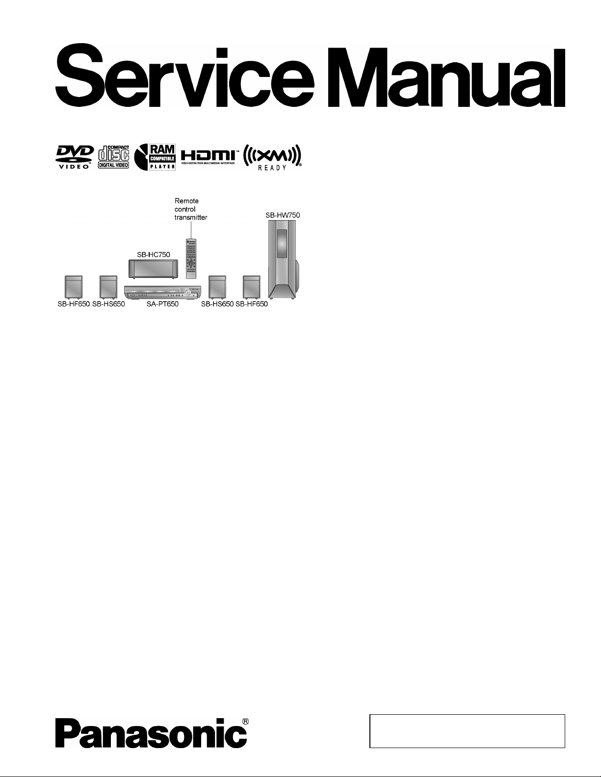
Page 1
A
ORDER NO. MD0702002CE
A6
DVD Home Theater Sound System
SA-PT650P
SA-PT650PC
Colour
(S).......................Silver Type
Specifications
lGENERAL
Power Supply:
Power Consumption: 135 W
Dimensions (W×H×D):
Mass:
Operating Temperature Range: +5°C to +35°C (+41°F to
Operating Humidity Range: 5% to 90% RH (no
lAMPLIFIER SECTION
RMS Output Power: Dolby Digital Mode
lTotal RMS Dolby Digital mode power:
At 1 kHz and total harmonic of 10%
lFront Ch: 125 W / Channel (3 Ω )
lCenter Ch: 250 W / Channel (6 Ω )
lSurround Ch: 125 W / Channel (3 Ω )
At 100 Hz and total harmonic of 10%
lSubwoofer Ch: 250 W / Channel (6 Ω )
FTC Output Power: Dolby Digital Mode
lTotal FTC Dolby Digital mode power:
At 120 Hz - 20 kHz and total harmonic of 1%
lFront Ch: 63 W / Channel (3 Ω )
lCenter Ch: 113 W / Channel (6Ω)
C 120 V, 60 Hz
430×70×424 mm
(16-15/16”×2-15/16”×16-11/16”)
Main unit 5 kg (11.02 Ibs)
+95°F)
condensation)
1000 W
428 W
lSurround Ch: 34 W / Channel (3Ω)
At 45 Hz - 120 Hz and total harmonic of 1%
lSubwoofer Ch: 121 W / Channel (6Ω)
lFM/AM TUNER, TERMINALS SECTION
Preset Memory:
Frequency Modulation (FM)
Frequency range: 87.9-107.9 MHz
Sensitivity: 2.5 µV (IHF)
S/N 26 dB: 2.2 µV
Antenna terminals:
Amplitude Modulation (AM/MW):
Frequency range: 520-1710 kHz (10-kHz step)
AM Sensitivity S/N 20 dB at
1000 kHz:
Phone Jack:
Terminal: Stereo, 3.5 mm (1/8”) jack
Music Port (Front):
Sensitivity: 100 mV, 1.2 kΩ
Terminal (Input): Stereo, 3.5 mm (1/8”) jack
lDISC SECTION
Discs played [8 cm (3”) or 12 cm (5”)]:
FM 30 stations
AM / MW 30 stations
(200-kHz step)
87.5-108.0 MHz
(100-kHz step)
75 Ω (unbalanced)
560 µV/m
© 2007 Matsushita Electric Industrial Co., Ltd. All
rights reserved. Unauthorized copying and
distribution is a violation of law.
Page 2
V
SA-PT650P / SA-PT650PC
(1) DVD (DVD-Video)
(2) DVD-RAM [DVD-VR, MP3 (*2, 5), JPEG (*4, 5)]
(3) DVD-R [DVD-Video, DVD-VR, MP3 (*2, 5), JPEG (*4, 5)]
(4) DVD-R DL (DVD-Video, DVD-VR)
(5) DVD-RW [DVD-Video, DVD-VR, MP3 (*2, 5), JPEG (*4, 5)]
(6) +R, +RW (Video)
(7) +R DL (Video)
(8) CD, CD-R/RW [CD-DA, Video CD, SVCD (*1), MP3 (*2, 5),
WMA (*3, 5), JPEG (*4, 5), HighMAT Level 2 (Audio and
Image)]
*1 Conforming to IEC62107
*2 MPEG-1 Layer 3, MPEG-2 Layer 3
*3 Windows Media Audio Ver.9.0 L3
lNot compatible with Multiple Bit Rate (MBR)
*4 Exif Ver 2.1 JPEG Baseline files
lPicture resolution: between 160 x 120 and 6144 x 4096
pixels (Sub sampling is 4:0:0, 4:2:0, 4:2:2 or 4:4:4).
Extremely long and narrow pictures may not be displayed.
*5 The total combined maximum number of recognizable audio
and picture contents and groups: 4000 audio and picture
contents and 400 groups
Pick Up:
Wavelength:
lCD: 785 nm
lDVD: 662 nm
Laser power:
lCD / DVD: (P) CLASS I / CLASS II
lCD / DVD: (PC) CLASS 1M / CLASS 1
Audio Output (Disc):
Number of channels: 5.1 ch (FL, FR, C, SL, SR,
lVIDEO SECTION
ideo System:
Composite Video Output:
lOutput level: 1 Vp-p (75 Ω )
lTerminal: Pin jack (1 system)
Component Video Output (480p/480i):
lY output level: 1 Vp-p (75 Ω )
lPBoutput level: 0.7 Vp-p (75 Ω )
lPRoutput level: 0.7 Vp-p (75 Ω )
lTerminal: Pin jack (Y: green, PB: blue,
HDMI AV Output:
lTerminal: Type A connector (19-pin),
Power Consumption in Standby Mode:
Note:
1. Specifications are subject to change without notice.
Mass and dimensions are approximate.
2. Total harmonic distortion is measured by the digital spectrum
analyzer.
Solder:
This model uses lead free solder (PbF).
SW)
NTSC
P
: red) (1 system)
R
approx. 0.5 W
Mechanism:
This model uses RC1U (Rotary tray) mechanism.
Refer to the respective original service manuals for *1, *2, *3,
*4.
CEC Ver.1.3a
2
Page 3
SA-PT650P / SA-PT650PC
CONTENTS
Page Page
1 Safety Precautions 5
1.1. GENERAL GUIDELINES
1.2. Before Repair and Adjustment
1.3. Protection Circuitry
1.4. Safety Parts Information
2 Prevention of Electro Static Discharge (ESD) to
Electrostatically Sensitive (ES) Devices
3 Precaution of Laser Diode
4 About Lead Free Solder (PbF)
4.1. Service caution based on legal restrictions
5 Handling Precaution s for Traverse Unit
5.1. Cautions to Be Taken in Handling the Optical Pickup Unit
5.2. Grounding for electrostatic breakdown prevention
6 Accessories
7 Operation Procedures
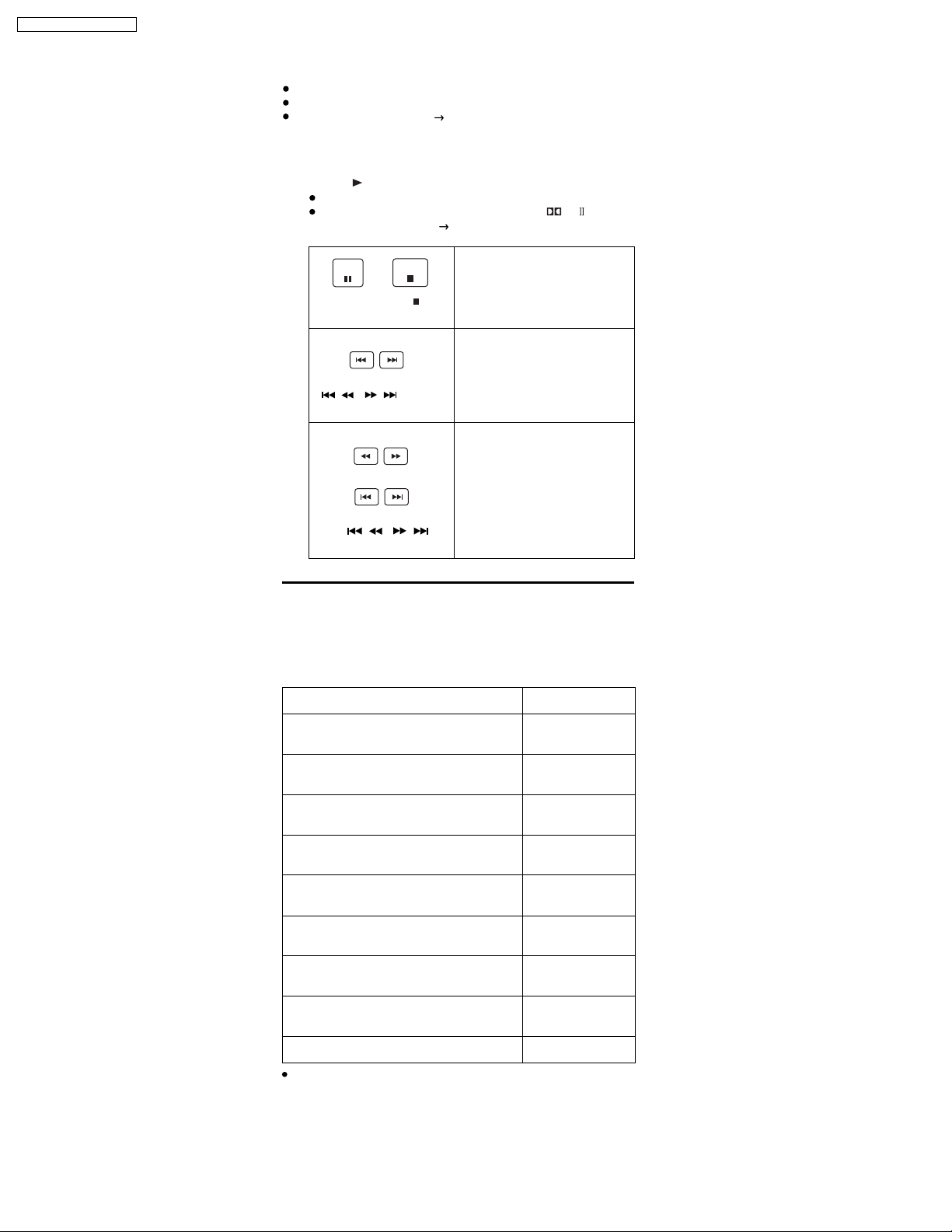
7.1. Remote Control Key Buttons Operations
7.2. Main Unit Key Buttons Operations
7.3. Using the EZ Sync HDAVI Control
7.4. Using the XMョ Satellite Radio
7.5. Using the Music Port
7.6. About iPod
7.7. Disc Information
8 New Features
8.1. About HDMI
8.2. Wireless Features
9 Self-Diagnosis and Special Mode Setting
9.1. Service Mode Summary Table
9.2. Service Mode Table (Main Unit)
9.3. Wireless Service Mode Summary Table
9.4. Service Mode Table (Wireless)
9.5. DVD Self Diagnostic Function-Error Code
9.6. Sales Demonstration Lock Function
9.7. Service Precautions
10 Assembling and Disassembling
10.1. Disassembly Flow Chart
10.2. Main Components and P.C.B. Locations
10.3. Disassembly of Top Cabinet
10.4. Disassembly of Tray Lid Assembly
10.5. Disassembly of Front Panel
10.6. Disassembly of Panel P.C.B. & Key P.C.B.
10.7. Dissassembly of Tray Base Assembly
10.8. Disassembly of Mechanism Base Assembly
10.9. Disassembly of Rear Panel
10.10. Disassembly of XM Module P.C.B.
10
10
11
11
11
13
14
14
15
16
17
18
19
21
23
23
25
32
32
32
42
43
45
49
50
51
53
54
55
55
55
56
56
57
57
58
10.11. Disassembly of Wireless Adapter P.C.B.
5
5
6
6
8
9
10.12. Disassembly of Tray P.C.B.
10.13. Disassembly of D-Amp P.C.B
10.14. Disassembly of Digital Amp IC (IC5000)
10.15. Disassembly of DVD Module P.C.B.
10.16. Disassembly of Main P.C.B.
10.17. Disassembly of Regulator IC (IC2903)
10.18. Disassembly of SMPS & AC-Inlet P.C.B.
10.19. Disassembly of D-Port P.C.B.
10.20. Disassembly of Switch Regulator IC (IC5701)
10.21. Disassembly of Regulator Diode (D5803)
10.22. Disassembly of Regulator Diodes (D5801 & D5802)
10.23. Disassembly of Regulator Diode (D5702)
10.24. Disassembly of Tray Guide (L) & Tray Guide (R)
10.25. Disassembly of Rotary Tray
10.26. Disassembly of Open Lock Gear
10.27. Disassembly of Close Lock Gear
10.28. Disassembly of Tray Motor P.C.B.
10.29. Disassembly of Sensor P.C.B.
10.30. Disassembly of Traverse Unit
10.31. Disassembly of Pulley Gear
10.32. Disassembly of Loading Motor P.C.B.
10.33. Disassembly of Drive Gear (A) & Drive Gear (B)
10.34. Disassembly of Magnet Holder, Washer, Magnet &
Clamper
10.35. Disassembly of Support Piece, Change Lever, Slide Plate
(L) & Slide Plate (R)
10.36. Disassembly of Cam Gear
10.37. Assembly of Tray Base Assembly
11 Service Fixture and Tools
12 Service Positions
12.1. Checking & Repair XM Module P.C.B.
12.2. Checking & Repair D-Port P.C.B.
12.3. Checking & Repair Panel P.C.B. & Key P.C.B.
12.4. Checking & Repair Main P.C.B.
12.5. Checking & Repair SMPS P.C.B.
12.6. Checking & Repair D-Amp P.C.B.
12.7. Checking & Repair DVD Module P.C.B.
13 Measurements and Adjustments
13.1. Service Tools and Equipment
13.2. Important points in adjustment
13.3. Storing and handling of test discs
13.4. Optical adjustment
14 Abbreviati ons
15 Voltage and Waveform Chart
58
59
59
60
60
61
62
62
63
63
64
64
65
65
65
66
66
67
67
67
68
68
69
69
70
71
71
72
72
72
72
72
73
74
74
74
76
76
76
76
77
78
80
3
Page 4

SA-PT650P / SA-PT650PC
15.1. DVD Module P.C.B. 80
15.2. Main P.C.B.
15.3. D-Amp P.C.B.
15.4. SMPS P.C.B.
15.5. XM Module P.C.B.
15.6. Panel P.C.B.
15.7. D-Port, Tray Motor, Loading Motor, Sensor & Tray P.C.B.
15.8. Waveform Chart
16 Illustration of IC's, Transistors and Diodes
17 Wiring Connection Diagram
18 Block Diagram
18.1. System Control
18.2. DVD (Servo)
18.3. DVD (Video/Audio)
18.4. DVD Interface
18.5. Audio
18.6. Audio Digital Amp
18.7. Power
19 Schematic Diagram Notes
20 Schematic Diagram
20.1. DVD Module (DV5/HDMI) Circuit
20.2. XM Module & Main Circuit
20.3. D-Port & Panel Circuit
20.4. D-Amp & SMPS Circuit
82
83
84
84
84
85
86
88
89
91
91
92
93
94
95
96
97
99
101
101
106
111
113
20.5. Tray, Key, Wireless Adapter, AC-Inlet & Loading Motor
Circuit
20.6. Tray Motor, Sensor & Optical Pickup Unit Circuit
21 Printed Circuit Board
21.1. DVD Module P.C.B.
21.2. XM Module, D-Port & AC-Inlet P.C.B.
21.3. Main P.C.B.
21.4. Panel, Key & Wireless Adapter P.C.B.
21.5. D-Amp P.C.B.
21.6. SMPS P.C.B.
21.7. Tray, Loading Motor, Tray Motor & Sensor P.C.B.
22 Basic Troubleshooting Guide
22.1. Basic Troubleshooting Guide for Traverse Unit (DVD
Module P.C.B)
22.2. Basic Troubleshooting Guide for HDMI AV output
23 Overall Block for PT650
23.1. SC-PT650 Main Circuit Block
23.2. SC-PT650 SMPS Circuit Block
24 Terminal Function of ICs
24.1. IC2001 (C2CBYY000442): System Control IC
25 Exploded Views
25.1. Cabinet Parts Location
25.2. Packaging
26 Replacement Parts List
26.1. Component Parts List
117
119
121
121
122
123
124
125
126
127
129
129
130
132
132
133
134
134
135
137
139
140
141
4
Page 5
SA-PT650P / SA-PT650PC
1 Safety Precautions
1.1. GENERAL GUIDELINES
1. When servicing, observe the original lead dress. If a short circuit is found, replace all parts which have been overheated or
damaged by the short circuit.
2. After servicing, see to it that all the protective devices such as insulation barriers, insulation papers shields are properly
installed.
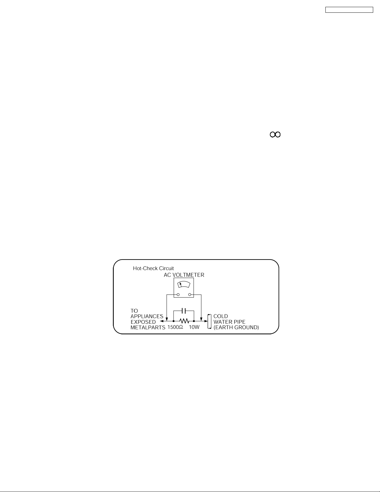
3. After servicing, carry out the following leakage current checks to prevent the customer from being exposed to shock hazards.
1.1.1. LEAKAGE CURRENT COLD CHECK
1. Unplug the AC cord and connect a jumper between the two prongs on the plug.
2. Measure the resistance value, with an ohmmeter, between the jumpered AC plug and each exposed metallic cabinet part on
the equipment such as screwheads, connectors, control shafts, etc. When the exposed metallic part has a return path to the
chassis, the reading should be between 1MΩ and 5.2MΩ.
When the exposed metal does not have a return path to the chassis, the reading must be
1.1.2. LEAKAGE CURRENT HOT CHECK
1. Plug the AC cord directly into the AC outlet. Do not use an isolation transformer for this check.
2. Connect a 1.5kΩ, 10 watts resistor, in parallel with a 0.15µF capacitors, between each exposed metallic part on the set and a
good earth ground such as a water pipe, as shown in Figure 1.
3. Use an AC voltmeter, with 1000 ohms/volt or more sensitivity, to measure the potential across the resistor.
4. Check each exposed metallic part, and measure the voltage at each point.
5. Reverse the AC plug in the AC outlet and repeat each of the above measurements.
6. The potential at any point should not exceed 0.75 volts RMS. A leakage current tester (Simpson Model 229 or equivalent) may
be used to make the hot checks, leakage current must not exceed 1/2 milliamp. In case a measurement is outside of the limits
specified, there is a possibility of a shock hazard, and the equipment should be repaired and rechecked before it is returned to
the customer.
Figure 1
1.2. Before Repair and Adjustment
Disconnect AC power to discharge unit AC Capacitors as such C5700, C5701, C5703, C5704, C5705 through a 10 Ω,10W
resistor to ground.
Caution:
DO NOT SHORT-CIRCUIT DIRECTLY (with a screwdriver blade, for instance), as this may destroy solid state devices.
After repairs are comple ted, restore power gradually using a variac, to avoid overcurrent.
Current consumption at AC 120 V, 60 Hz in NO SIGNAL mode volume minimal should be ~ 900 mA.
5
Page 6
SA-PT650P / SA-PT650PC
1.2.1. Caution for fuse replacement
1.3. Protection Circuitry
The protection circuitry may have operated if either of the following conditions are noticed:
· No sound is heard when the power is turned on.
· Sound stops during a performance.
The function of this circuitry is to prevent circuitry damage if, for example, the positive and negative speaker connec tion wires are
“shorted”, or if speaker systems with an impedance less than the indicated rated impedance of the amplifier are used.
If this occurs, follow the procedure outlines below:
1. Turn off the power.
2. Determine the cause of the problem and correct it.
3. Turn on the power once again after one minute.
Note:
When the protection circuitry functions, the unit will not operate unless the power is first turned off and then on again.
1.4. Safety Parts Information
Safety Parts List:
There are special components used in this equipment which are important for safety.
These parts are marked by
should be replaced with manufacturer’s specified parts to prevent shock, fire or other hazards. Do not modify the original design
without permission of manufacturer.
Reference No. Part No. Part Name & Description Remarks
PC5701 B3PBA0000402 PHOTO COUPLER [M]
PC5702 B3PBA0000402 PHOTO COUPLER [M]
PC5720 B3PBA0000402 PHOTO COUPLER [M]
PC5799 B3PBA0000402 PHOTO COUPLER [M]
D5701 B0FBAR000041 DIODE [M]
DZ5701 ERZV10V511CS ZENER [M]
TH5701 D4CAA5R10001 THERMISTOR [M]
TH5860 D4CC11040013 THERMISTOR [M]
L2101 J0JBC0000015 CHIP INDUCTOR [M]
L2201 J0JBC0000015 CHIP INDUCTOR [M]
L2802 J0JBC0000015 CHIP INDUCTOR [M]
L2803 J0JBC0000015 CHIP INDUCTOR [M]
L2804 J0JBC0000015 CHIP INDUCTOR [M]
L2805 J0JBC0000015 CHIP INDUCTOR [M]
L5001 G0B9R5K00003 CHOKE COIL [M]
L5002 G0B9R5K00003 CHOKE COIL [M]
L5201 G0B9R5K00003 CHOKE COIL [M]
L5301 G0B9R5K00003 CHOKE COIL [M]
L5401 G0B9R5K00003 CHOKE COIL [M]
L5402 G0B9R5K00003 CHOKE COIL [M]
L5500 J0JKB0000020 EMI BEAD CORE [M]
L5501 J0JKB0000020 EMI BEAD CORE [M]
L5702 ELF22V035B COIL [M]
L5721 J0JKB0000020 EMI BEAD CORE [M]
T2900 G4D1A0000117 TRANSFORMER [M]
T5701 ETS42BM15GAD TRANSFORMER [M]
in the Schematic Diagrams & Replacement Parts List. It is essential that these critical parts
Table 1
6
Page 7

Reference No. Part No. Part Name & Description Remarks
T5751 ETS19AB236AG TRANSFORMER [M]
F1 K5D802APA008 FUSE [M]
FP2902 K5H5012A0010 FUSE PROTECTOR [M]
P5701 K2AB2B000010 JACK [M]
A2 K2CB2CB00018 AC CORD [M]
C5700 F1BAF1020020 1000P [M]
C5701 ECQU2A334MLA 0.33 [M]
C5703 ECQU2A224MLC 0.22 [M]
C5704 F1BAF1020020 1000P [M]
C5705 F1BAF1020020 1000P [M]
SA-PT650P / SA-PT650PC
7
Page 8

SA-PT650P / SA-PT650PC
2 Prevention of Electro Static Discharge (ESD) to
Electrostatically Sensitive (ES) Devices
Some semiconductor (solid state) devices can be damaged easily by static electricity. Such components commonly are called
Electrostatically Sensitive (ES) Devices. Examples of typical ES devices are integrated circuits and some field-effect transistors and
semiconductor "chip" components. The following techniques should be used to help reduce the incidence of component damage
caused by electro static discharge (ESD).
1. Immediately before handling any semiconductor component or semiconductor-equipped assembly, drain off any ESD on your
body by touching a known earth ground. Alternatively, obtain and wear a commercially available discharging ESD wrist strap,
which should be removed for potential shock reasons prior to applyin g power to the unit under test.
2. After removing an electrical assembly equipped with ES devices, place the assembly on a conductive surface such as
aluminum foil, to prevent electrostatic charge buildup or exposure of the assembly.
3. Use only a grounded-tip soldering iron to solder or unsolder ES devices.
4. Use only an anti-static solder removal device. Some solder removal devices not classified as "anti-static (ESD protected)" can
generate electrical charge sufficient to damage ES devices.
5. Do not use freon-propelled chemicals. These can generate electrical charges sufficient to damage ES devices.
6. Do not remove a replacement ES device from its protective package until immediately before you are ready to install it. (Most
replacement ES devices are packaged with leads electrically shorted together by conductive foam, aluminum foil or comparable
conductive material).
7. Immediately before removing the protective material from the leads of a replacement ES device, touch the protective material
to the chassis or circuit assembly into which the device will be installed.
Caution:
Be sure no power is applied to the chassis or circuit, and observe all other safety precautions.
8. Minimize bodily motions when handling unpackaged replacement ES devices. (Otherwise harmless motion such as the
brushing together of your clothes fabric or the lifting of your foot from a carpeted floor can generate static electricity (ESD)
sufficient to damage an ES device).
8
Page 9
SA-PT650P / SA-PT650PC
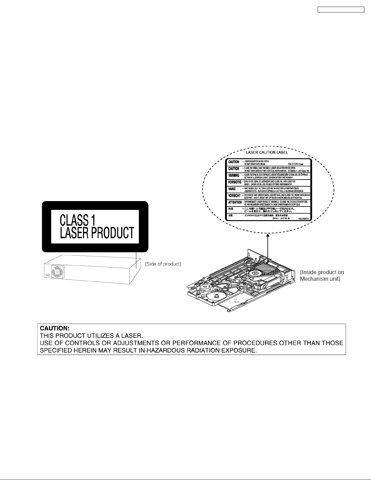
3 Precaution of Laser Diode
CAUTION:
This unit utilizes a Class I/Class II (P), Class 1M/Class 1 (PC) laser.
Invisible laser radiation is emitted from the optical pickup lens.
Wavelength: 662nm(DVD)/785nm(CD).
Maximum output radiation power from pickup: 100µW/VDE
When the unit is turned on:
1. Do not look directly into the pick up lens.
2. Do not use optical instruments to look at the pick up lens.
3. Do not adjust the preset variable resistor on the pickup lens.
4. Do not disassemble the optical pick up unit.
5. If the optical pick up is replaced, use the manufacturer’s specified replacement pick up only.
6. Use of control or adjustments or performance of procedures other than those specified herein may result in hazardous
radiation exposure.
9
Page 10
SA-PT650P / SA-PT650PC
4 About Lead Free Solder (PbF)
4.1. Service caution based on legal restrictions
4.1.1. General description about Lead Free Solder (PbF)
The lead free solder has been used in the mounting process of all electrical components on the printed circuit boards used for this
equipment in considering the globally environmental conservation.
The normal solder is the alloy of tin (Sn) and lead (Pb). On the other hand, the lead free solder is the alloy mainly consists of tin
(Sn), silver (Ag) and Copper (Cu), and the melting point of the lead free solder is higher approx.30 degrees C (86°F) more than that
of the normal solder.
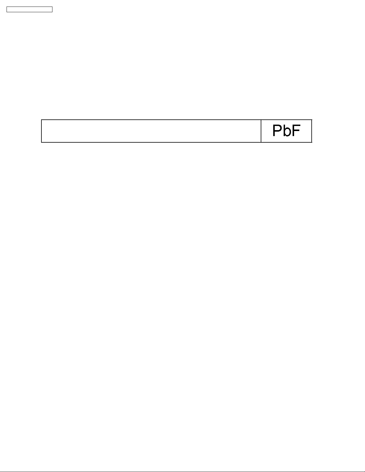
Definition of PCB Lead Free Solder being used
The letter of “PbF” is printed either foil side or components side on the PCB using the lead free solder.
(See right figure)
Service caution for repair work using Lead Free Solder (PbF)
· The lead free solder has to be used when repairing the equipment for which the lead free solder is used.
(Definition: The letter of “PbF” is printed on the PCB using the lead free solder.)
· To put lead free solder, it should be well molten and mixed with the original lead free solder.
· Remove the remaining lead free solder on the PCB cleanly for soldering of the new IC.
· Since the melting point of the lead free solder is higher than that of the normal lead solder, it takes the longer time to melt
the lead free solder.
· Use the soldering iron (more than 70W) equipped with the temperature control after setting the temperature at 350±30
degrees C (662±86°F).
Recommended Lead Free Solder (Service Parts Route.)
· The following 3 types of lead free solder are available through the service parts route.
RFKZ03D01K-----------(0.3mm 100g Reel)
RFKZ06D01K-----------(0.6mm 100g Reel)
RFKZ10D01K-----------(1.0mm 100g Reel)
Note
* Ingredient: tin (Sn), 96.5%, silver (Ag) 3.0%, Copper (Cu) 0.5%, Cobalt (Co) / Germanium (Ge) 0.1 to 0.3%
10
Page 11
SA-PT650P / SA-PT650PC
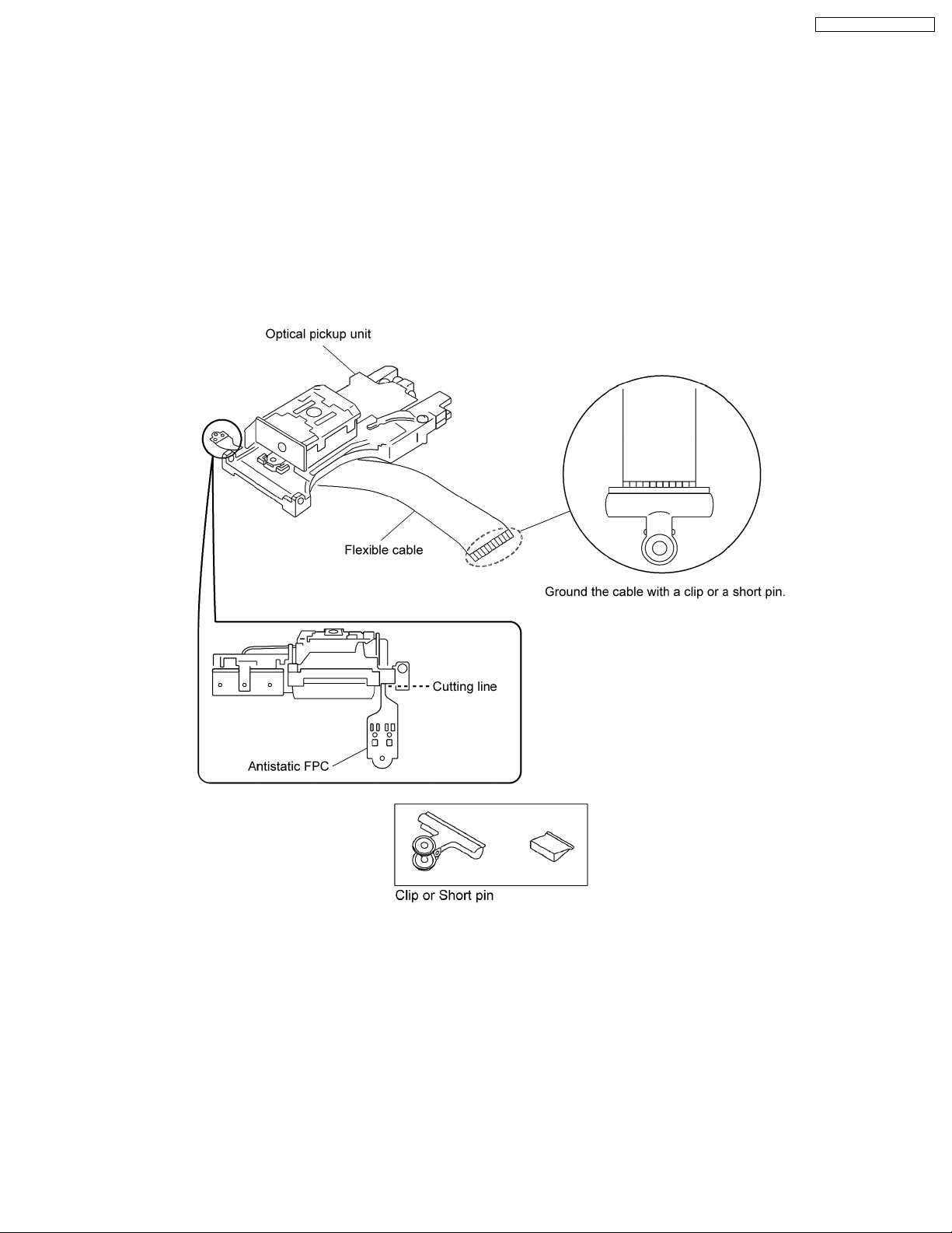
5 Handling Precautions for Traverse Unit
The laser diode in the optical pickup unit may break down due to static electricity of clothes or human body. Special care must be
taken avoid caution to electrostatic breakdown when servicing and handling the laser diode.
5.1. Cautions to Be Taken in Handling the Optical Pickup Unit
The laser diode in the optical pickup unit may be damaged due to electrostatic discharge generating from clothes or human body.
Special care must be taken avoid caution to electrostatic discharge damage when servicing the laser diode.
1. Do not give a considerable shock to the optical pickup unit as it has an extremely high-precise structure.
2. To prevent the laser diode from the electrostatic discharge damage, the flexible cable of the optical pickup unit removed should
be short-circuited with a short pin or a clip.
3. The flexible cable may be cut off if an excessive force is applied to it. Use caution when handling the flexible cable.
4. The antistatic FPC is connected to the new optical pickup unit. After replacing the optical pickup unit and connecting the flexible
cable, cut off the antistatic FPC.
5.2. Grounding for electrostatic breakdown prevention
Some devices such as the DVD player use the optical pickup (laser diode) and the optical pickup will be damaged by static
electricity in the working environment. Proceed servicing works under the working environment where grounding works is
completed.
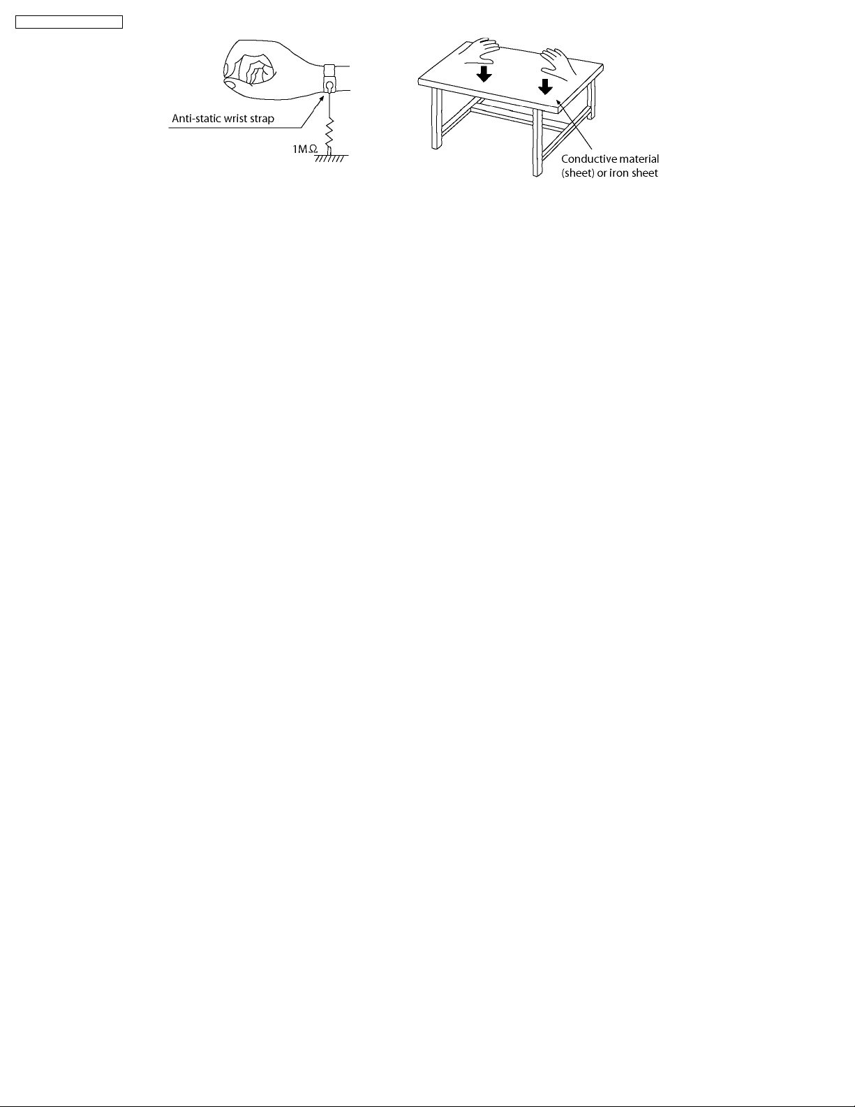
5.2.1. Worktable grounding
1. Put a conduc tive material (sheet) or iron sheet on the area where the optical pickup is placed, and ground the sheet.
5.2.2. Human body grounding
1. Use the anti-static wrist strap to discharge the static electricity form your body.
11
Page 12
SA-PT650P / SA-PT650PC
12
Page 13
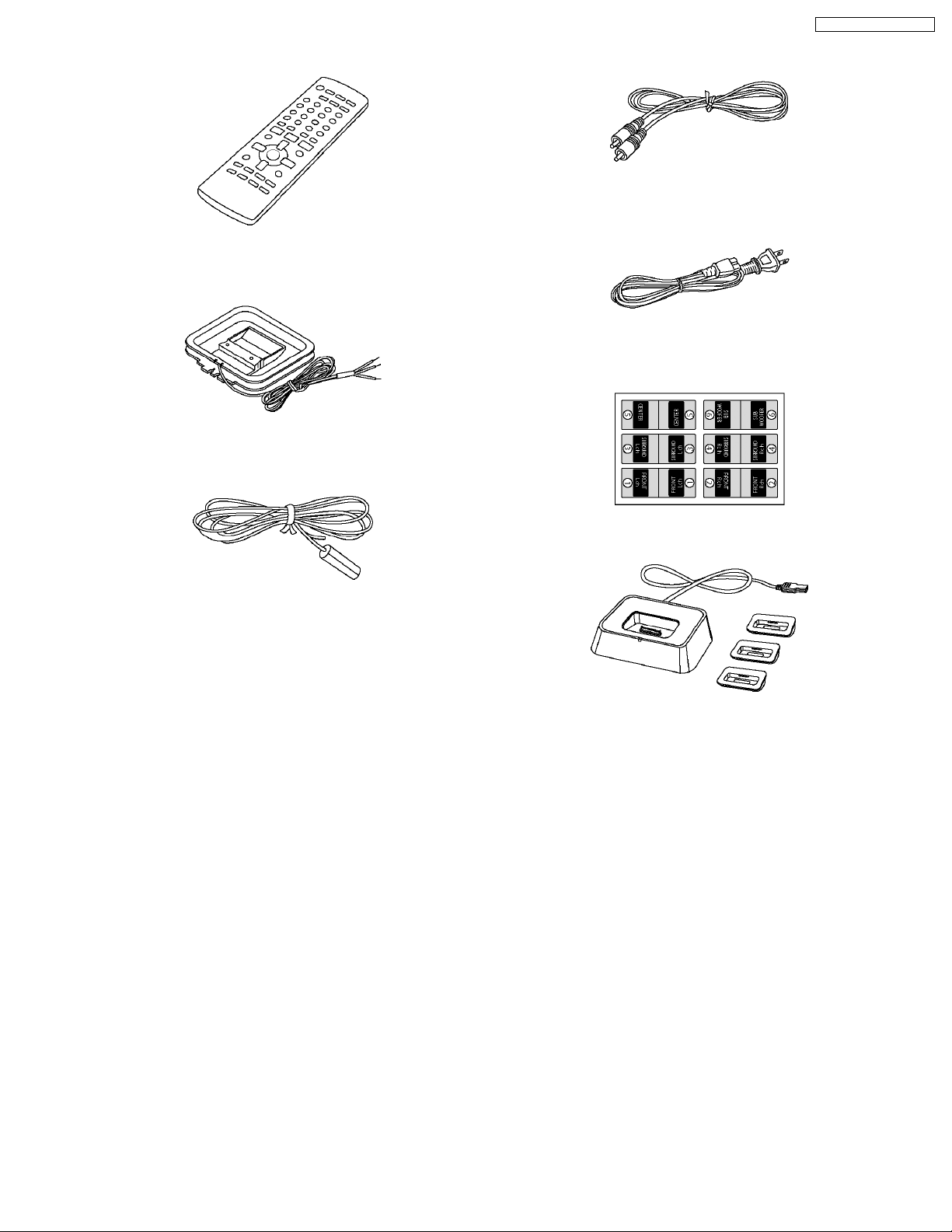
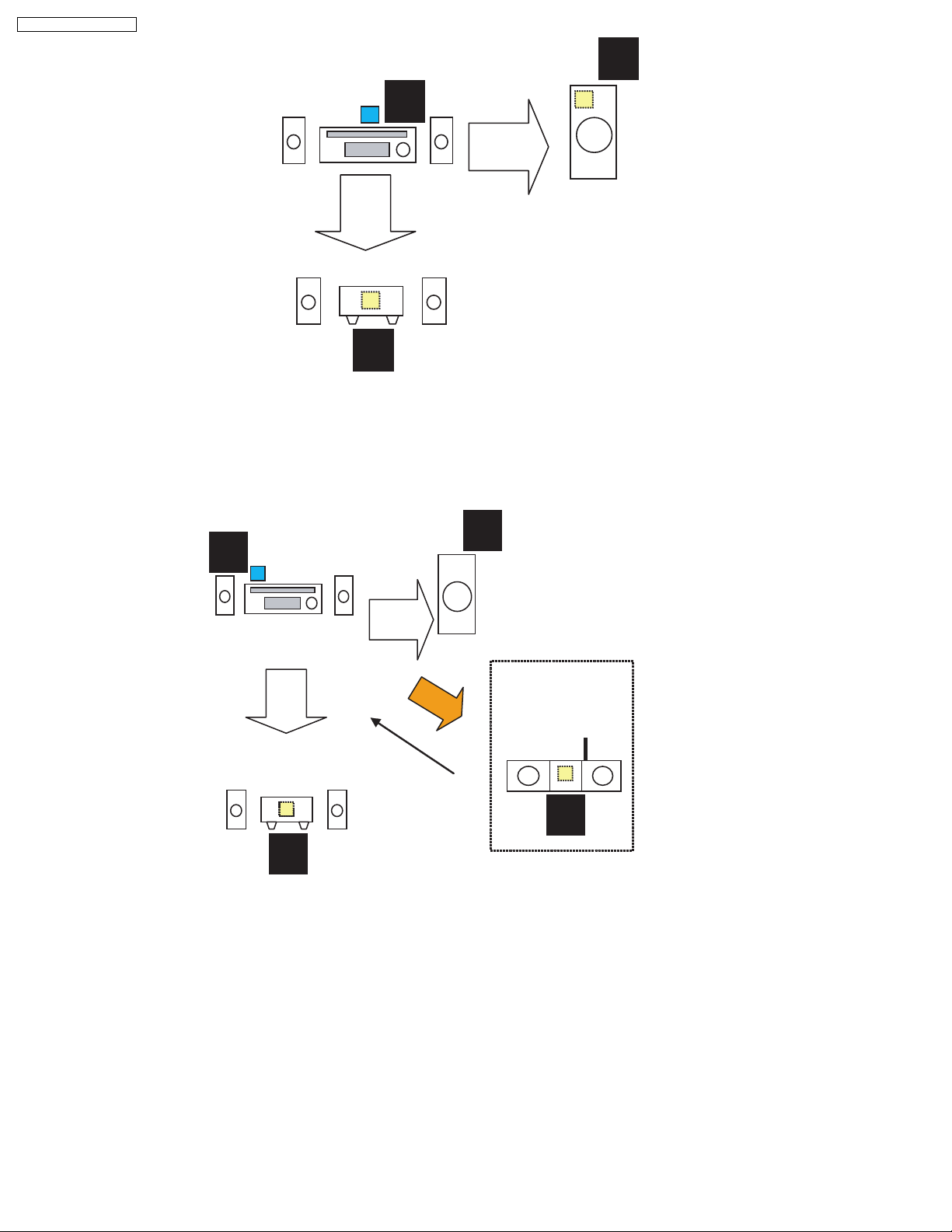
6 Accessories
Remote control
AM loop antenna
SA-PT650P / SA-PT650PC
Video Cable
AC cord
FM antenna
Speaker label
iPod cradle
13
Page 14
SA-PT650P / SA-PT650PC
7 Operation Procedures
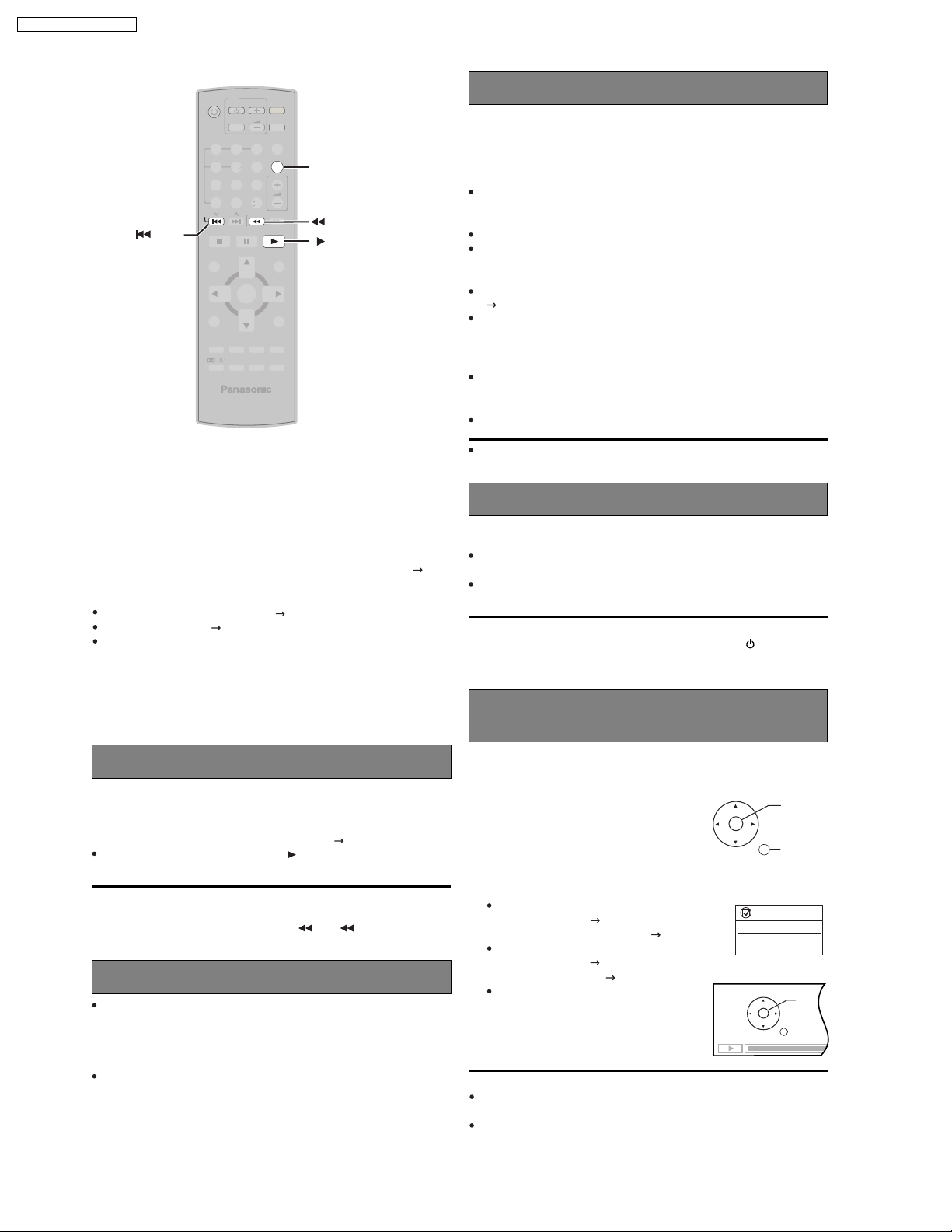
7.1. Remote Control Key Buttons Operations
Television operations
Turn the main unit on/off
Select the source
[DVD]: DVD/CD
[TUNER/BAND]:
[EXT-IN]: MUSIC P. , AUX , OPTION
FM/AM , XM
Select disc s title numbers etc./Enter numbers
Select the disc or show disc information
Select preset radio stations/channels
Basic operations for play
Show a disc top menu or program list
Frame-by-frame/ Select or register menu items on the
television screen / Browse XM radio categories
Show on-screen menu
-
EQ
-
TEST
SW.LEVEL
-
SLEEP
PLAY MODE
-
CH SELECT
-
PL
CD MODE
FL DISPLAY
CANCEL
S.SRD
-
Mute the sound
MUTING flashes in the main unit s display while the
function is on.
To cancel, press the button again or adjust the volume.
Muting is canceled when you switch the unit to standby.
Start up and play a disc automatically
Adjust the volume of the main unit
Select radio stations/channels manually
Show a disc menu or play list
Return to previous screen
or show the setup menu
This function is available only when using the optional
Panasonic wireless sound system SH-FX85.
:
[2ND SELECT]
MAIN SOURCE (follows the selected source for the
main room (FM AM)
Return to MAIN SOURCE
If the main room is in FM/AM mode, you can only
*
select the same mode for the FM/AM tuner of the
second room.
For details, refer to the operating instructions for the
optional Panasonic wireless sound system SH-FX85.
Turn the unit off automatically (Sleep timer)
1 Press and hold the button.
2 While the time is shown, press the button repeatedly to select
the time (in minutes).
The maximum setting is 120-min (in 30-min steps)
Press and hold the button again to confirm the remaining time
on the unit s display.
To cancel, select "OFF" in the main unit’s display.
Change the source for the second
room
*
XM OPTION
14
Page 15
7.2. Main Unit Key Buttons Operations
SA-PT650P / SA-PT650PC
Standby/on switch [POWER ]
Turn the main unit on/off.
Press to switch the unit from on to
standby mode or vice versa. In standby
mode, the unit is still consuming a small
amount of power.
5 DISC SELECTOR
Select a disc directly
SELECTOR
DVD /CD F M A M XM
AUX MUSIC P. OPTION
Return to DVD/CD
/ -TUNE MODE / FM MODE
Stop playing/
Select the tuning mode
Adjust the FM reception condition
Play discs/
Memorize the receivngi
radio stations/channels
Remote control signal sensor
Display
,
Skip or slow-search play/
Select the radio stations/channels
TUNING
/MEMORY
MUSIC PORT
Connect an external
device
VOLUME
Adjust the volume
of the main unit.
OPEN/CLOSE
Open/Close the disc drawer
DISC EXCHANGE
Open the disc drawer to
exchange the disc in the play
position
DISC SKIP
Skip to the next disc tray
Headphones
(not included)
Headphone plug type:
Reduce the volume before
connecting.
Audio is automatically switched to
2-channel stereo.
To prevent hearing damage, avoid
listening for prolonged periods of
time.
3.5 mm (
1
/8) stereo mini plug
"
15
Page 16
PLAY
RETURN
SKIP
PAUSE
SKIP
STOP
SA-PT650P / SA-PT650PC
7.3. Using the EZ Sync HDAVI Control
TV
DVD
VOLUME
TV/VIDEO
TUNER/BAND
EXT-IN
3
SKIP
12
4
7
DISC
SKIP
TOP MENU
DIRECT
NAVIGATOR
FUNCTIONS
CANCEL-CD MODE
PL
S.SRD
56
89
0
SLOW/SEARCH
ENTER
-
EQ
-
SW.LEVEL
-
SLEEP
FL DISPLAY
PLAY MODE
-
CH SELECT
-
TEST
10
ONE TOUCH PLAY
VOLUME
PLAYPAU S ESTOP
MENU
PLAY LIST
-
RETURN
-
SETUP
2ND
SELECT
MUTING
ONE TOUCH PLAY
SLOW/SEARCH
PLAY
What is EZ Sync HDAVI Control?
EZ Sync HDAVI Control is a convenient function that offers linked
operation of this unit and Panasonic TV (VIERA) with EZ Sync HDAVI
Control. You can use this function by connecting the equipment with the
HDMI cable. For operational details, see the operating instructions of the
connected equipment.
This unit supports "HDAVI Control 2"
function.
The TV with "HDAVI Control 2" function enables the following operation:
EZ Sync Control only with TV s remote control (for "HDAVI Control 2")( right)
Preparation
Confirm that the HDMI connection ( OI page 6) has been made.
Set "EZ Sync" to "On" ( OI page 24, "HDMI" menu).
To complete and activate the connection correctly, turn on all
HDAVI Control
compatible equipment and set the television to the
EZ Sync
corresponding HDMI input mode for the home theater system.
Speaker control
You can select whether audio is output from the home theater system or
the television speakers by using the television menu settings. For details,
refer to the operating instructions of your television.
Home theater
Theater speakers are active.
When the home theater system is in standby mode, changing the television
speakers to theater speakers in the televison menu will automatically turn
the home theater system on and select "AUX
" as the source.
The television speakers are automatically muted.
You can control the volume setting using the volume or mute button on
the TV s remote control. (The volume level is displayed on the main
unit s FL display.)
To cancel muting, you can also use the home theater remote control
( OI page 10).
If you turn off the home theater system, television speakers will be
automatically activated.
TV
Television speakers are active.
The volume of the home theater system is set to "0".
This function works only when "DVD/CD" or "AUX " is selected as the
source on the home theater system.
Audio output is 2-channel audio.
When switching between the theater and television speakers, the TV
screen may be blank for several seconds.
Power off link
When the television is turned off, the home theater system goes into
standby mode automatically.
This function works only when "DVD/CD" or "AUX" is selected as the
source on the home theater system.
When the television is turned on, the home theater system does not turn
on automatically. (Power on link is not available.)
[Note]
Only the home theater system turns off when you press [ ] for shutting it
down. Other connected equipment compatible with EZ Sync HDAVI
Control stay on.
Whenever the connection or settings are changed, reconfirm the points
above.
One touch play
You can turn on the home theater system and television, and start playing
the disc in the play position with a single press of a button.
Press [ONE TOUCH PLAY].
Theater speakers will be automatically activated ( right ).
This function also works if you press [ PLAY] on the home theater
remote control during home theater standby mode.
[Note]
Playback may not be immediately displayed on the television. If you miss
the beginning portion of playback, press [ ] or [ ] to go back to
where playback started.
Auto input switching
When you switch the television input to:
TV tuner mode, the home theater system will automatically switch to
"AUX".
HDMI input mode for the home theater system, the home theater
system will automatically switch to "DVD/CD" if it is in "AUX " mode.
When you start disc play, the television will automatically switch to the
HDMI input mode for the home theater system.
EZ Sync Contol only with TV’s remote
control (for "HDAVI Control 2")
You can control the disc menus of the home theater system with the TV s
remote control when using the t "DVD/CD" source. When operating the
TV s remote control, refer to the below illustration for operation buttons.
1 Select the theater operation menu by using
the television menu settings.
(For details, refer to the operating instructions
of your television.)
The home theater system will automatically
switch to "DVD/CD" if it is in "AUX" mode.
2 Select the desired item.
"TOP MENU": Shows a disc top menu
OI page
(
15, 18)
or
program list ( OI page 19).
"MENU": Shows a disc menu
OI page
"Control P anel":
(
list (
The basic operations for
15, 18)
OI page 19).
or play
discs are available.
[Note]
Depending on the menu, some button operations cannot be performed
from the TV s remote control.
"Control Panel" can be selected directly by using a button on the TV s
remote control (e.g. [SUB MENU]).
ENTER/
PLAY
RETURN
EZ Sync
TOP MENU
MENU
Control Panel
16
Page 17
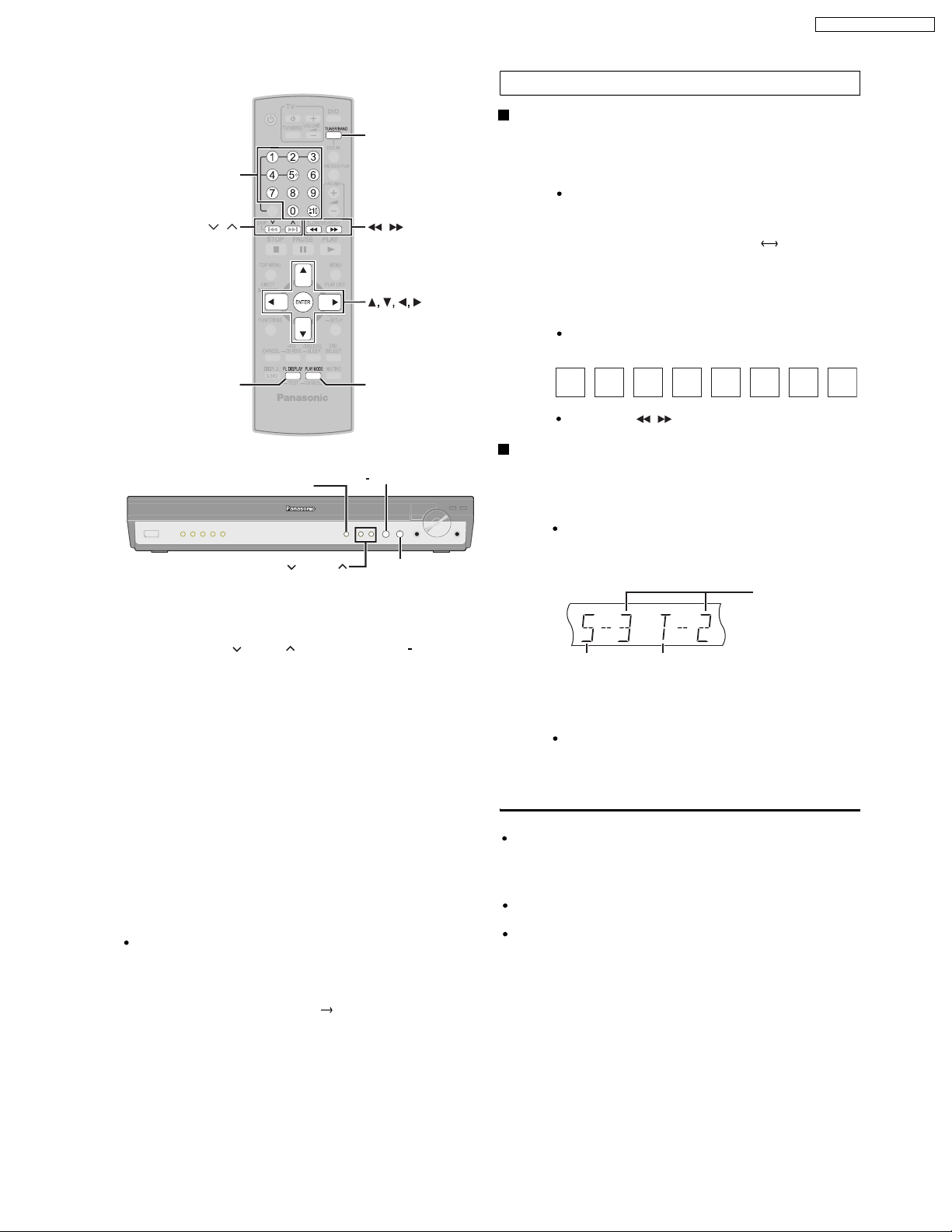
7.4. Using the XM® Satellite Radio
TUNER/BAND
Numbered
buttons
Preparation
The XM Satellite Radio ID
Please confirm your XM Satellite Radio ID necessary for activating
XM Satellite Radio as follows.
1
Press [TUNER/BAND] to select "XM".
1
Ensure the antenna is connected (OI page7).
*
SA-PT650P / SA-PT650PC
,
FL DISPLAY
SELECTOR
TUNING
Radio operations are described mainly with the remote control.
You can alternatively use the corresponding button on the main unit.
1
[SELECTOR] [ TUNING ] [MEMORY] [ TUNE MODE]
*
XM Satellite Radio
XM Satellite Radio is the provider of satellite radio. XM offers more than
170 digital radio channels with music, talk, news, sports, comedy, traffic
and weather reports. To enjoy XM Satellite Radio, subscription is
required.
For more information, visit XM on the Web at www.xmradio.com for U.S.
customers, or www.xmradio.ca for Canada customers.
How to Subscribe
XM monthly service subscription sold separately. XM Connect & Play
antenna, or XM Passport Mini-Tuner and Home Dock (includes home
antenna) required to receive XM service (sold separately). Channels with
frequent explicit language are indicated with an XL. Channel blocking is
available for XM radio receivers by calling 1-800-XMRADIO (U.S.
residents) or 1-877-GET-XMSR (Canada residents). Subscriptions
subject to Customer Agreement available at xmradio.com (U.S. residents)
and xmradio.ca (Canada residents). Only available in the 48 contiguous
United States and Canada. C 2006 XM Satellite Radio Inc. All rights
reserved. All other trademarks are the property of their respective owners.
To subscribe in the U.S., visit
XM s Listener Care at 1-800-XMRADIO (1-800-967-2346).
To subscribe in Canada, visit
XM s Listener Care at
2
*
XM on the Web at www.xmradio.com or call
XM on the Web at
1-877-GET-XMSR
3
*
(1-877-438-9677).
,
, ENTER
PLAY MODE
TUNE MODE
MEMORY
4
*
www.xmradio.ca
or call
4
Press [PLAY MODE] to select "MANUAL".
2
Each time you press the button: MANUAL PRESET
Press [0] to select "XM 0" (XM channel 0).
3
"RADIO ID" is indicated in the display briefly, followed by
an 8-digit alphanumeric ID.
Note your XM Satellite Radio ID.
4
To avoid ambiguity, the letters I, O, S and F are not used in
the ID.
To exit, press [ ]
*
2
to select another channel.
*
,
Optimizing the XM signal reception
The main unit has a signal strength indicator function that allows you
to optimize the XM signal reception.
1
Press [TUNER/BAND] to select "XM".
1
Ensure the antenna is connected (OI page 7).
Press and hold [FL DISPLAY] until the XM signal
2
status is displayed.
DISC
S.SRD
USB
DVD
CD
MODE
Satellite signal
Position the antenna for the best possible satellite
3
signal reception.
The display changes depending on the signal strength.
If the satellite signal is weak or not available, you can
optimize for the terrestrial signal (where available).
Press [FL DISPLAY] to return to the previous
4
display.
TG
Tips for optimizing reception
To prevent interference with wireless equipment, place the antenna away
from this unit, Panasonic wireless sound system SH-FX80/SH-FX85,
Panasonic wireless system SH-FX50/SH-FX60/SH-FX65, and other
equipment that emits radio waves (such as radio equipment and
microwave ovens).
Place the antenna near a south-facing window with an unobstructed
view of the sky for the best satellite signal reception.
Refer also to the operating instructions of your XM antenna.
*
MONO
KARA
D.M IX
Terrestrial signal
SLP
ST CT
PGM
EQ
Signal strength:
4 (strong)
PL
DDTS
3 (good)
SRDE.
PRG
RDS
RND
2 (marginal)
WS
W1 W2
1 (weak)
0 (no signal)
You should have your Radio ID ready ( right).
17
Page 18
SA-PT650P / SA-PT650PC
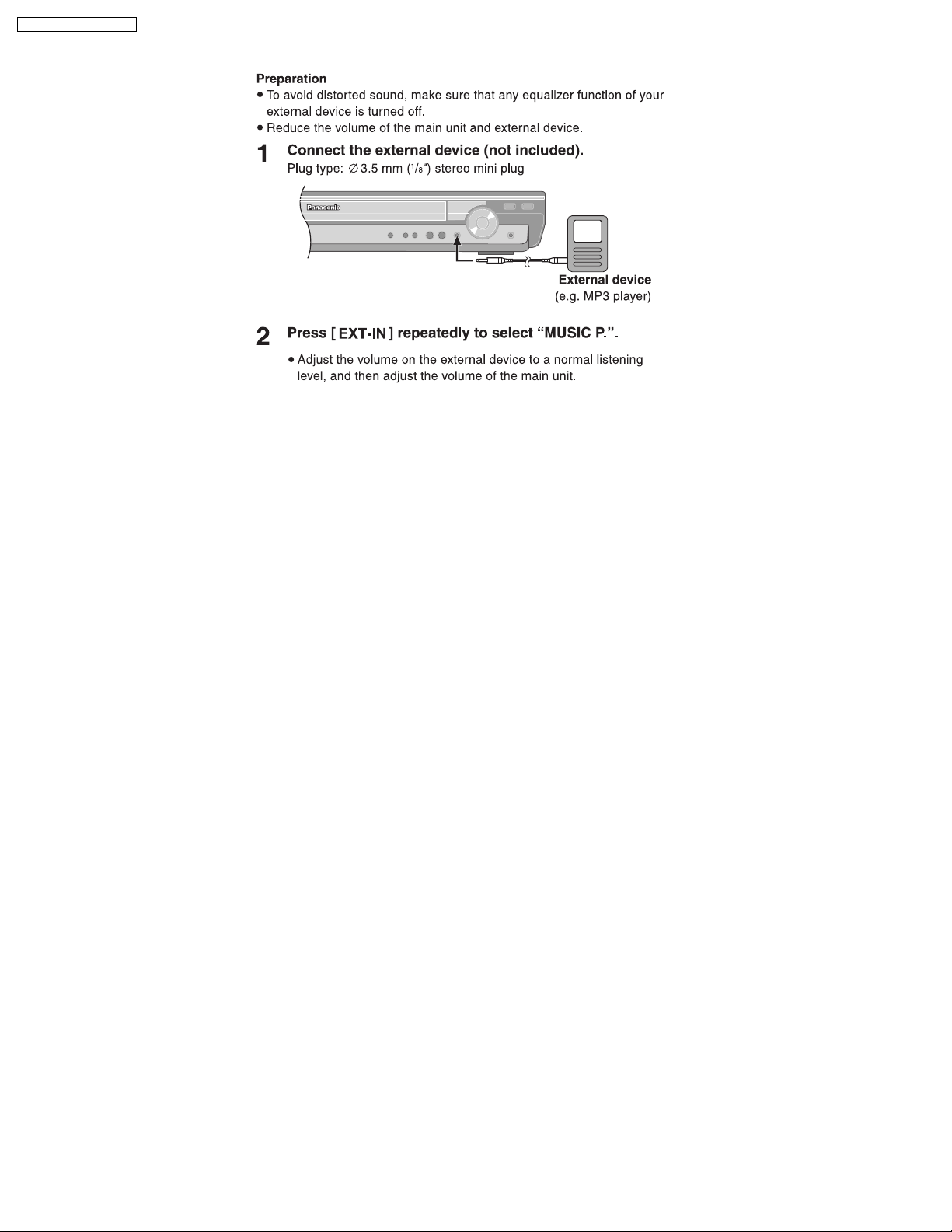
7.5. Using the Music Port
18
Page 19
7.6. About iPod
[11]
[10]
[9]
7.6.1. iPod Connection
SA-PT650P / SA-PT650PC
Dock adapter for
i
Pod nano 2nd generation
(aluminum)
(2GB, 4GB, 8GB)
11
The mark
[11]
For other types of iPod, please use the dock adapter sold separately.
[10]
Dock adapter for
iPod 5th generation
(video) (60GB, 80GB)
10
or
[9]
is shown on the back of each dock adapter.
Dock adapter for
iPod 5th generation
(video) (30GB)
9
Connect the dock to
the back of the main
unit.
OPTION V .1
Do not connect
or disconnect the
dock while the
main unit is on.
Universal Dock
for iPod
When removing,
insert your
fingernail or a
flat object and lift
upwards.
Charging the iPod
iPod (not included)
the iPod is inserted, and
charging starts.
Charging time
iPod nano 2nd generation (aluminum)
iPod 5th generation (video)
iPod nano 1st generation
iPod 4th generation (color display)
iPod 4th generation
iPod mini
[Note]
AC cord must be connected with the main unit.
"OPTION " will be shown on the main unit’s display during iPod
charging in main unit standby mode. It will go off when charging
is finished.
For the above models under "fixed 5-hour charging",
"OPTION " continues to be displayed throughout this duration,
even when your iPod is fully charged. You can turn off this display
by removing the iPod from the dock.
Compatibility depends on the software version of your iPod.
The indicator lights up when
Until iPod is fully charged
5 hours (fixed)
19
Page 20
SA-PT650P / SA-PT650PC
7.6.2. Using the iPod
Preparation
Adjust the volume on the iPod to a normal listening level.
Reduce the volume of the main unit.
Confirm the iPod connection ( OI page 8).
Press [ EXT-IN ] repeatedly to select "OPTION".
1
The iPod turns on.
Press [ PLAY] to play th e iPod.
2
Adjust the volume of the main unit.
You can enjoy surround sound when you press [ /S.SRD] to
turn on Super Surround (
OI page 30).
PL
PAUSE
Alternatively, press [ ] on
the main unit.
(During play/pause)
Alternatively, press
[, ] on
/
the main unit.
(During play/pause)
or press and hold
Alternatively, press and
hold [ , ]
on the main unit.
When you select another source, or turn the main unit off, the iPod turns
off.
STOP
To pause track
To skip a track
/
To search the current track
/
/
[Note]
Image/video display through the home theater is not available.
Compatible iPod
Name Memo ry siz e
iPod nano
2nd generation (aluminum)
iPod
5th generation (video)
iPod
5th generation (video)
iPod nano
1st generation
iPod
4th generation (color display)
iPod
4th generation (color display)
iPod
4th generation
iPod
4th generation
iPod mini 4GB, 6GB
Compatibility depends on the software version of your iPod.
2GB, 4GB, 8GB
60GB, 80GB
30GB
1GB, 2GB, 4GB
40GB, 60GB
20GB, 30GB
40GB
20GB
20
Page 21
7.7. Disc Information
7.7.1. Disc Playability (Media)
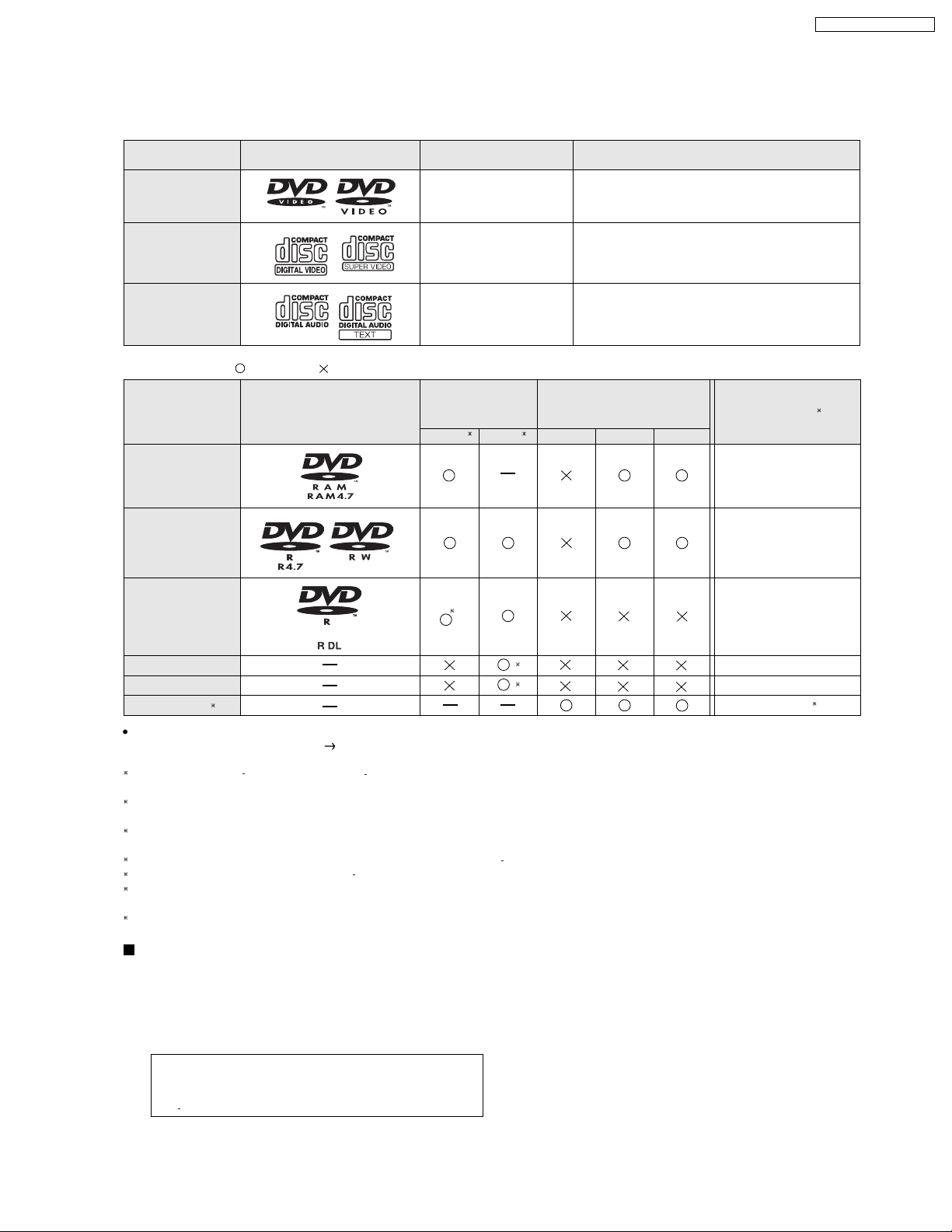
Commercial discs
Disc
Logo
Indicated in these
instructions by
SA-PT650P / SA-PT650PC
Remarks
DVD- Vi deo
Video CD
CD
Recorded discs ( )
Disc
: Playable, : Not playable
Logo
DVD-RAM
DVD-R/RW
DVD-R DL
[DVD-V]
[VCD]
[CD]
Recorded on a
DVD vi d eo
recorder, etc.
[DVD-VR]
2
[DVD-V]
3
High quality movie and music discs
Music discs with video
Including SVCD (Conforming to IEC62107)
Music discs
Recorded on a personal
computer, etc.
4
[WMA] [MP3] [JPEG]
Finalizing
Not Necessary
Necessary
Necessary
6
+
+
R/ RW
+R DL
CD-R/RW
It may not be possible to play all the above-mentioned discs in some cases due to the type of disc, the condition of the recording, the recording
method, or how the files were created
1
This unit can play CD-R/RW recorded with CD-DA or Video CD format.
[WMA] [MP3] [JPEG] This unit also plays HighMAT discs.
2
Discs recorded on DVD video recorders or DVD video cameras, etc. using Version 1.1 of the Video Recording Format (a unified video recording
standard).
3
Discs recorded on DVD video recorders or DVD video cameras using Version 1.2 of the Video Recording Format (a unified video recording
standard).
4
Discs recorded on DVD video recorders or DVD video cameras using DVD-Video Format.
5
Recorded using a format different from DVD-Video Format, therefore some functions cannot be used.
6
A process that allows play on compatible equipment. To play a disc that is indicated as "Necessary", the disc must first be finalized on the device it
was recorded on.
7
Closing the session will also work.
1
[ Refer to Section 7.7.2. File Extension Type Support (WMA/MP3/JPEG)]
()
()
5
5
Necessary
Necessary
Necessary
7
Discs that cannot be played
DVD-RW version 1.0, DVD-Audio, DVD-ROM, CD-ROM, CDV,
CD-G, SACD, DivX Video Disc and Photo CD, DVD-RAM that
cannot be removed from their cartridge, 2.6-GB and 5.2-GB
DVD-RAM, and "Chaoji" VCD available on the market including
CVD, DVCD, and SVCD that do not conform to IEC62107.
Note about using a DualDisc
The digital audio content side of a DualDisc does not meet the
technical specifications of the Compact Disc Digital Audio
(CD-DA) format so playback may not be possible.
21
Page 22
SA-PT650P / SA-PT650PC
7.7.2. File Extension Type Support (WMA/MP3/JPEG)
Format Disc Extension Reference
[WMA] CD-R/RW ".WMA"
".wma"
[MP3] DVD-RAM
DVD-R/RW
".MP3"
".mp3"
CD-R/RW
[JPEG] DVD-RAM
DVD-R/RW
CD-R/RW
".JPG"
".jpg"
".JPEG"
".jpeg"
When there are more than 8 groups, the eighth group onwards will be displayed on one vertical line in the menu screen.
There may be differences in the display order on the menu screen and computer screen.
This unit cannot play files recorded using packet write.
Compatible compression rate: between 48 kbps and 320 kbps
You cannot play WMA files that are copy-protected.
This unit does not support Multiple Bit Rate (MBR: an encoding process for audio content that
produces an audio file encoded at several different bit rates).
Compatible compression rate:
between 32 kbps and 320 kbps for sampling frequencies of 32 kHz and above
between 8 kbps and 160 kbps for sampling frequencies of 24 kHz and below
This unit does not support ID3 tags.
Compatible sampling frequencies:
DVD-RAM, DVD-R/RW:
11.02, 12, 22.05, 24, 44.1 and 48 kHz
CD-R/RW:
8, 11.02, 12, 16, 22.05, 24, 32, 44.1 and 48 kHz
JPEG files taken on a digital camera that conform to DCF Standard (Design rule for Camera
File system) Version 1.0 are displayed.
Files that have been altered, edited or saved with computer picture editing software may not
be displayed.
This unit cannot display moving pictures, MOTION JPEG and other such formats, still pictures
other than JPEG (e.g. TIFF), or play pictures with attached audio.
Naming folders and files
(Files are treated as contents and
folders are treated as groups on this
unit.)
At the time of recording, prefix folder and
file names. This should be with numbers
that have an equal number of digits, and
should be done in the order you want to
play them (this may not work at times).
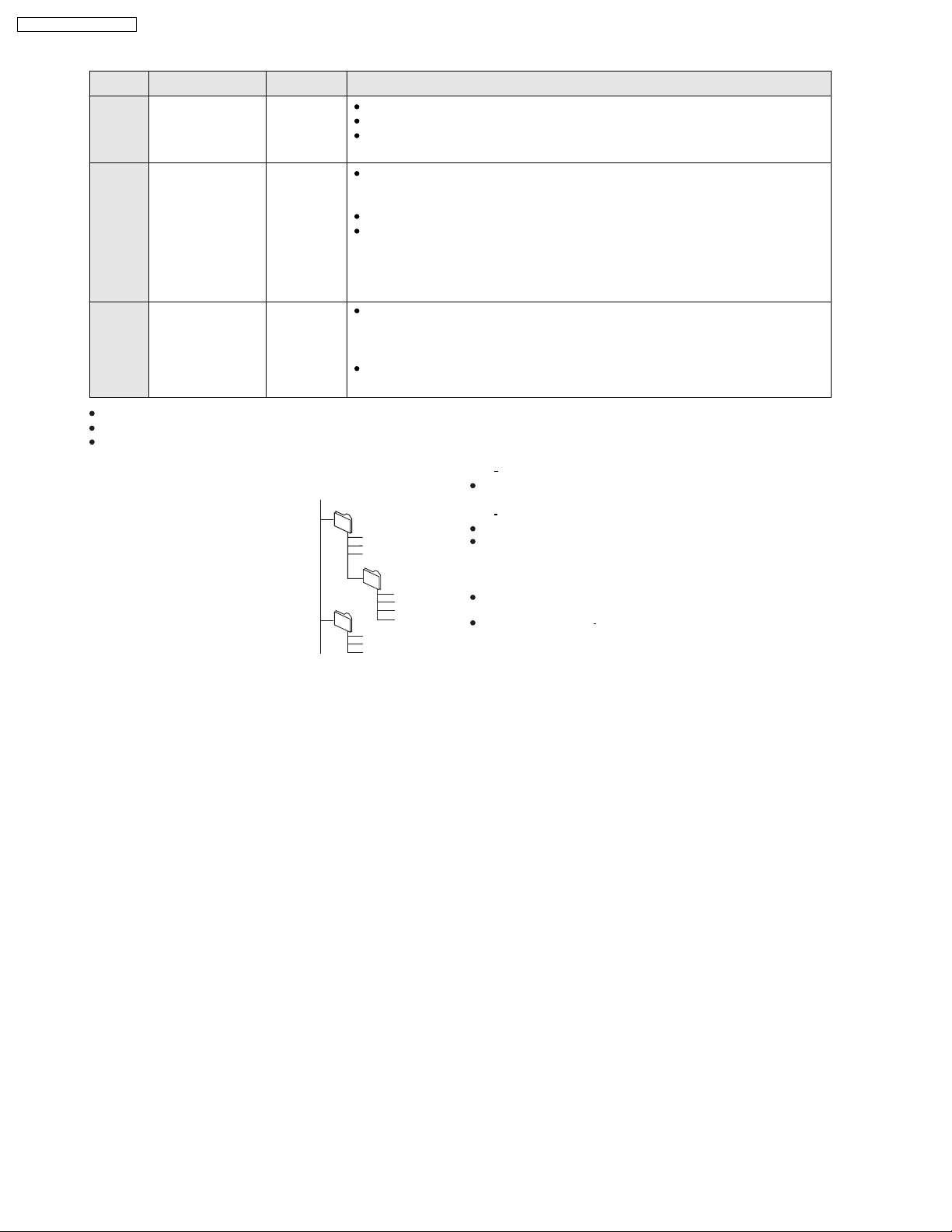
e.g.
root
[MP3]
001 group
001
003 group
001 track.mp3
002 track.mp3
003 track.mp3
002 group
001 track.mp3
002 track.mp3
003 track.mp3
004 track.mp3
001 track.mp3
002 track.mp3
003 track.mp3
DVD RAM
Discs must conform to UDF 2.0.
DVD R/RW
Discs must conform to UDF bridge (UDF 1.02/ISO9660).
This unit does not support multi-session. Only the default session is
played.
CD-R/RW
Discs must conform to ISO9660 level 1 or 2 (except for extended
formats).
This unit supports multi session but if there are many sessions it takes
more time for play to start. Keep the number of sessions to a minimum
to avoid this.
22
Page 23
8 New Features
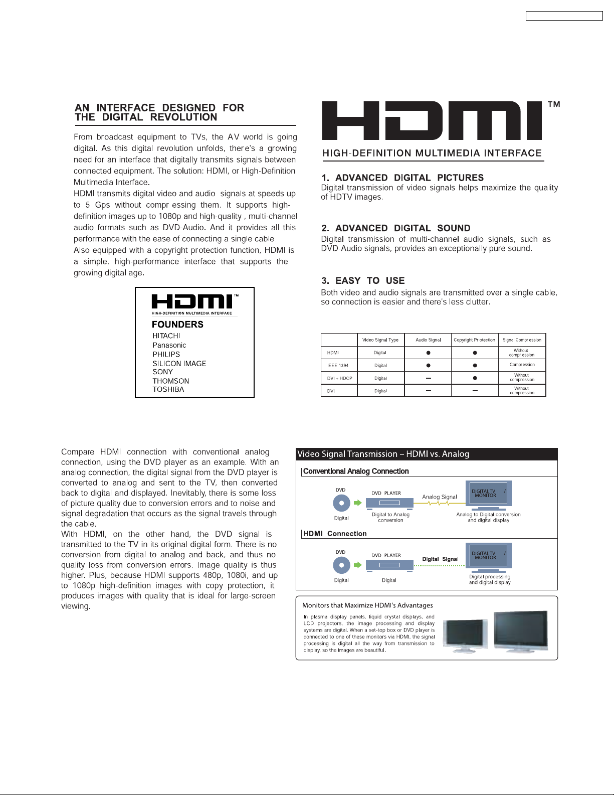
8.1. About HDMI
8.1.1. What is HDMI?
SA-PT650P / SA-PT650PC
8.1.2. Advanced Digital Pictures
23
Page 24

SA-PT650P / SA-PT650PC
8.1.3. Advanced Digital Sound
8.1.4. Easy to Use
8.1.5. HDMI Compatible Products
24
Page 25
SA-PT650P / SA-PT650PC
8.2. Wireless Features
8.2.1. Function Overview
Year 2007 PT models support wireless which includes FX65/FX66, wireless subwoofer and FX85 as described below:-
8.2.1.1. FX65/FX66
· The FX65/FX66 supports one-way wireless transmission only, that is, it will only transmit wireless audio signal to the rear
surround speakers. The FX65/FX66 receiver module includes a D-AMP and SMPS. The transmitter interfaces with the main unit
using serial communications to communicate information such as mute command request, link detection and ID setting request.
Maximum range attainable is 15 meters.
8.2.1.2. Wireless Subwoofer (For PT1050 only)
· The wireless subwoofer receiver module is similar in operation with FX65/FX66 in such a way that it only supports one-way
wireless transmission. It also includes a D-AMP and SMPS. The differe nce in the wireless subwoofer receiver module is the way
its hardware interprets the audio it receives from the transmitter since it is the same audio received by the FX65/FX66 receiver.
Maximum range attainable is 30 meters.
8.2.1.3. FX85
· The FX85 supports the multi-room function wherein it operates as a second room wireless receiver (up to a maximum of two).
Maximum range attainable is 30 meters. It can send commands to the main unit to control functions such as Play, Stop,
Forward Skip/Channel Up, Reverse Skip/Channel Down. It also has a built-in DAP pocket for stand-alone operation by inserting
a DAP device (e.g. iPod) in the DAP pocket to play the device only via the device’s own control buttons, FX85 cannot control
the device using its own buttons. The transmitter interfaces with the main unit using serial communications to communicate
information such as mute command request, link detection, ID setting request and button commands from the FX85 buttons
(Play, Stop, Forward Skip/Channel Up, Reverse Skip/Channel Down). The FX85 receiver module has the following
functions/terminals/buttons:
FX85 BUTTONS FX85 FUNCTIONS
FX 85 Power Button D-Amp
Selector Button SMPS
Play Button D-Port Connector
Stop Button ID Set Switch
Forward Skip/Channel Up MPort
Reverse Skip/Channel Down
Volume Control
25
Page 26
SA-PT650P / SA-PT650PC
8.2.2. Block Diagram
· There are two types of transmitter cards, Type A and Type B, and two types of receiver modules, Type 1 and Type 2 for the
wireless configuration. The block diagrams below describe the differences of each of the types.
8.2.2.1. TX-TYPE A / RX-TYPE 1
Note:
RF
RF
EEPROM
EEPROM
- One way only
- FX65/FX66 signal flow
- FX65/FX66 only
BB
MCU
ADC
CH2
IN
TX Type A
· Type A transmitter uses one ADC (Analog to Digital Converter) and transmits audio through Channel 2. Type 1 receiver (Rx)
uses one DAC and output audio through Channel 2. The firmware (that is downloaded to EEPROM) multiplexes which channel
to listen to (in this case Channel 2 since type A is transmitting from channel 2 In) by setting the baseband accordingly.
DAC
CH2
OUT
BB
RX Type 1
MCU
26
Page 27
8.2.2.2. TX-TYPE B / RX-TYPE 2
S
RF
EEPROM
BB
MCU
ADC
ADC
DAC
RF
BB
EEPROM
MCU
SA-PT650P / SA-PT650PC
Note:
- FX65/FX66 SIGNAL FLOW
- FX85 S
- ONE WAY AND
SIMULTANEOUS
- FX65/FX66 + FX85
- FX65/FX66 TRANSMITTER NOT
USED, NEED TO IDSET
FX65/FX66
- TX TYPE B BUT RX
CHANGED FROM TYPE 2
TO TYPE 1, CH1 SIGNAL
REDIRECTED TO DAC
IGNAL FFLOW
CH2
IN
CH1 IN
TX Type B
CH2
OUT
RX Type 2
· Type B transmitter uses two ADC (Analog to Digital Converter) to send audio streams from Channel 1 and Chann el 2 for the
FX65/FX66 surround sound and FX85 second room audio, respectively. Type 2 receiver outputs audio through Channel 2. The
software multiplexes which channel to listen to by setting the baseband accordingly. For example, if the receiver is configured
as an FX85 receiver (Type 2), the baseband is configured to accept Channel 1 audio transmission and redirect it to Channel
2 Out. If the receiver is set as an FX65/FX66 or wireless subwoofer, the baseband is configured to accept channel 2 audio
transmission and redirect it to the same Channel 2 Out.
8.2.3. Activation
· FX65/FX66 can be activated in the main unit by using either transmitter Type A or Type B and enabling surround sound by
selecting Surround Music, DPL or Super Surround (Music/Movie).
· FX85 Wireless feature is enabled by default when the user uses transmitter type B.
8.2.4. LED Indication
· For FX65/FX66, there will be two-color LED that will be used to indicate Power On and Link. If link, the two-color LED will be
green, else, it will be red.
For FX85, the front panel will have LED indicators for Standby,, Wireless Link, Charge, Option and Music Port. During Power
On, Standby LED will be OFF. Only during power OFF will this LED be ON (Red). Wireless Link indicator will be ON (Green)
when link is established between TX and RX and OFF when link is lost. Pressing the selector button will toggle from any of the
selector modes Wireless, Option and Music port. Only the currently selected mode will be ON (Green), the other two will be
OFF. Charge LED will be ON (Red) once iPod charging is initiated.
8.2.5. Key Operation (FX85)
· Selector Button
This button will be used to select Wireless, Option or M.Port and enabling the correspondin g LED indicators for each mode.
During Power On, by default, selector mode is set to Wireless when power is initially supplied to the system. But during Power
On/OFF button, it will remember the last selector mode setting.
· Play Button
This button will send command to the main unit to play CD/DVD as well as the iPod. This function is therefore meaningful only
27
Page 28

SA-PT650P / SA-PT650PC
if the second room selector is in Main Source (with the first room user in CD/DVD or iPod) and iPod.
· Stop Button
This button will send command to the main unit to stop CD/DVD as well as the iPod. This function is therefore meaningful only
if the second room selector is in Main Source (if the first room user is in CD/DVD mode or iPod) and iPod.
· Forward Skip/Channel Up
This button depends on the second room source currently selected. It will be interpreted as a Forward Skip by the main unit if
the second room source is in Main Source (with the first room user is in CD/DVD or iPod mode) and iPod. It will be interpreted
as a Channel Up (preset channels only) if the second room source is in FM, AM, or XM.
· Reverse Skip/Channel Down
This button depends on the second room source currently selected. It will be interpreted as a Reverse Skip by the main unit if
the second room source is in Main Source (if the first room user is in CD/DVD or mode) and iPod. It will be interpreted as a
Channel Down (preset channels only) if the second room source is in FM, AM, or XM.
· Volume Control
Volume control will be local to the FX85 module only. Default volume (TBD) will be set every time power is first supplied to the
system or during exit from stand by mode.
· ID-setting Operation
ID setting operation can be invoked by pressing fast-forward key in the main unit and three [3] key in the remocon. Once IDsetting is triggered, the receiver must press its ID-setting button within 60 seconds. During this period, the transmitter will be in
open connect mechanism whereby any receiver can pair with the transmitter. After this period elapsed, the transmitter will revert
back to using close connect code whereby only those receivers which have the same ID as the transmitter will be able to link.
The user also has the option to exit the ID setting operation by pressing the same keys.
· iPod Detection and Charging
iPod is detected once inserted on the FX85 and battery charging automatically starts.
−
− The iPod Charging in Standby Mode:
− −
lUpon iPod insertion detection and FX85 is in Power OFF (stand by), FX85 set will enter iPod charging Standby Mode.
lThe FX85’s CHARGE LED will light up whenever the iPod is charging.
lFX85 will charge the battery up to five hours. After this period, FX85 will not try to recharge the iPod.
lAfter battery full condition, even if the iPod is operated such as play, FX85 will not retry to recharge the iPod (timer will start
immediately once iPod is inserted).
lRe - charging of the battery in iPod Charging Standby Mode can be done only by removing and reinserting the iPod to the
dock.
−
− The iPod charging in Power On Mode:
− −
lThe iPod automatically charges its battery whenever it is connected during Power ON.
lThe FX85’s CHARGE LED will light up whenever the iPod is charging.
lFX85 will continue charging the iPod as long as it is inserted (no charging time limit of five hours).
28
Page 29
SA-PT650P / SA-PT650PC
8.2.6. FX Configurations
There are four types of configurations for the FX series. This is explained by the following illustrations below:
Case 1: FX65/FX66
· This is the basic configuration of FX65/FX66 whereby it is only receiving wireless surround audio signal from the main set. This
uses a Type A transmitter which is only able to send audio in one direction. Audio is sent using streams AB through Ch 2.
TX
A
RX
FX65/FX66
1
CH2/AB
Case 2 A: FX65/FX66 + FX85
· In this configuration, a second receiver, an FX85, in another room is listening to another audio source from the main set. The
FX85 also is able to send command to the main set such as Play, Stop, Skip, and Preset Tuner Channel Up/Down. This
configuration uses Type B transmitter which is an upgrade of the Type A and can be used on Type 1 (FX65/FX66). This
transmitter is able to send audio signal for second room via Ch 1 and first room via Ch 2.
In this configuration, streams AB is used to transmit the audio from main unit to the first room Type 1 receiver (FX65/FX66) via
Ch 2. While the second room audio is transmitted through stream CD via Ch 1.
TX
B
Multi-room + Multi source
RX
CH1/CD
CH2/AB
RX
1
FX65/FX66
Case 3 A: Wireless Subwoofer
· This configuration, Type A transmitter send signals to subwoofer and Type 1 receiver (FX65/FX66) via channel 2, which is the
same audio signals sent to FX65/FX66 as well. The subwoofer only decodes the low frequency signal.
1
FX85
29
Page 30
SA-PT650P / SA-PT650PC
1
RX
TX
A
CH2/AB
RX
1
Case 3 B: FX65/FX66 + FX85 + Wireless Subwoofer (for PTX7, PT1050)
· In this configuration, all audio source for the Type 1 subwoofer and Type 1 first room receiver (FX65/FX66) through streams AB
via Ch 2 and Type 2 second room receiver (FX85) comes from transmitter B through streams CD via Ch 1. For this
configuration, the user must perform ID setting for FX85 if it is sold as an accessory, but for bundled type, it already is paired
with the transmitter.
CH2/AB
B
CH2/AB
RX
RX
1
1
RX
CH2/AB
Multi-room + Multi source
CH1-CD
RX
1
30
Page 31

8.2.7. User Operation Flow
Y
START
Is Tx card
inserted?
N
Insert Tx card
SA-PT650P / SA-PT650PC
POWER ON MAINSET
Is there audio
source playing?
N
Play music
Is music heard on
wireless surround
speaker?
Y
DONE
TX-RX probably not
paired. Do ID setting
process
Y
N
Press FF Key in Mainset and 3 key
on remocon until "P" led displays
Is wireless link led
blinking?
Y
Press ID set button on receiver
Is wireless link led
blinking?
N
A
Y
CHECK FOR SPEAKER
WIRE CONNECTIONS
Is wireless
receiver on?
Power on receiver
A
Repeat ID set
process
8.2.8. Baseband Settings Update from EEPROM IC
· The software will read from an external EEPROM IC to get the selected baseband IC settings. Not all baseband register
settings (a total of 512 bytes) will be read from the EEPROM IC, though. Aside from getting the baseband settings from the
EEPROM IC, it is also used to enable FCC testing, select the application type and entering into doctor mode (this can be
enabled also by sendin g a command via the main unit).
8.2.9. Doctor Mode
· For normal operation but automatic frequency selection is disabled, it can enter into Doctor Mode. This feature is hidden from
normal user and will be used by the service center to fix to a particular RF Channel. With doctor mode, the user can disable
frequency automatic allocation and sniffer and be able to select a fix RF Channel (Channels 1, 2 or 3) by a combination or
remote control keys. Refer to Section 9.4 for Wireless Doctor Mode.
31
Page 32

SA-PT650P / SA-PT650PC
9 Self-Diagnosis and Special Mode Setting
9.1. Service Mode Summary Table
The service modes can be activated by pressing various button combination on the main unit and remote control unit.
Below is the summary for the various modes for checking:
Player buttons Remote control unit buttons Application Note
STOP 0 Error code check. (Refer to the section
5 Jitter checking.
PAUSE Initial setting of laser drive current.
FUNCTIONS DVD laser drive current check. (Refer to the section
1 ADSC internal RAM data check.
3 CD laser drive current check.
“9.2.1. Service Mode
Table 1” for more
information.)
“9.2.2. Service Mode
Table 2” for more
information.)
6 Region display and mode. (Refer to the section
7 Micro-processor firmware version check.
Initialization of the player (factory setting is restored).
Used after replacement of Micro-processor (DV5 LSI) IC, FLASH
ROM IC (IC8651), EEPROM IC (IC8611) and DVD Module
P.C.B.
8 DVD Module P.C.B. firmware version check. (Refer to the section
MENU Communication error display.
TOP MENU ECC error check.
EQ CPPM/CRM keys check.
ENTER DVD Module P.C.B. reset.
Timer 1 check. (Refer to the section
Timer 1 reset.
Timer 2 check.
Timer 2 reset.
STOP+ 1 Combination reliability test mode. (Refer to the section
2 OPEN/CLOSE reliability test mode.
3 Tray rotation reliability test mode.
“9.2.3. Service Mode
Table 3“ for more
information.)
“9.2.4. Service Mode
Table 4“ for more
information.)
“9.2.5. Service Mode
Table 5“ for more
information.)
“9.2.7.1. Test Mode List”
for more information.)
Note:
An error code will be canceled if a power supply is turned OFF.
*1: CPPM is the copy guard function beforehand written in the disk for protection of copyrights.
*2: CEC is the consumer electronic control used for high-level user control of HDMI-connected devices.
*3: HDCP is the specification developed to control digital audio & video contents transmission for DVI or HDMI connections.
9.2. Service Mode Table (Main Unit)
By pressing various button combinations on the main unit and remote control unit, you can activate the various service modes for
checking.
Special Note:
Due to the limitations of the no. characters that can be shown on the FL Display, the “FL Display” button on the remote control
unit can be used to show the two display pages. (Display 1 / Display 2).
· Refer to Section 7.1 for the section on “Remote Control Key Buttons Operations“.
32
Page 33

9.2.1. Service Mode Table 1
SA-PT650P / SA-PT650PC
Mode Name
Jitter check
Error code
check
Item
Description
Jitter check.
Jitter rate is measured and displayed.
Measurement is repeatedly done in
the cycle of one second. Read error
counter starts from zero upon mode
setting.
When target block data failed to be
read out, the counter advances by one
increment. When the failure is caused
by minor error, it may be corrected
when retried to enable successful
reading.
In this case, the counter advances by
one. When the error persists even
after retry, the counter may jump by
two or more.
FL Display sequence:
Display 1 2.
Error code check
The latest error code stored in the
EEPROM IC is displayed.
Note: Refer to "Section 9.5 DVD Self
Diagnostic Function-Error Code" for
more detailed information on the error
codes.
FL Display
(Display 1)
Jitter check
mode
Jitter rate is shown in decimal notation to
one place of decimal.
Focus drive value is shown in hexadecimal
notation.
(Display 2)
Lead
Error
Counter
Error code (play_err) is expressed in the
following convention.
Error code = 0 x DAXX is expressed: DVDnn U12
Error code = 0 x DBXX is expressed: DVDnn H12
Error code = 0 x DXXX is expressed: DVDnn F123
Error code = 0 x 0000 is expressed: DVDnn F--* "xx" denotes the error code
Jitter rate
Focus Drive
Value
U / H / F
Key Operation
Front Key
In STOP (no disc) mode,
press [STOP] button on the
main unit, and [5] button on
the remote control unit.
Press [POWER] button to
exit.
Press [FL Display] on
remote control unit for next
page (FL Display).
In STOP (no disc) mode,
press [STOP] button on the
main unit, and [0] button on
the remote control unit. * With
pointing of cursor up and
down on display.
Cancelled automatically
5 seconds later.
To exit, press [POWER]
button on main unit or
remote control.
Initial setting
of laser drive
current
Initial setting of laser drive current.
Initial current value for the DVD laser
and CD laser is separately saved in
the EEPROM IC.
FL Display sequence:
Display 1 2.
(Display 1)
Laser current
measurement
CD
Laser
mode
DVD Laser
The value denotes the current in decimal
notation.
(Display 2)
The above example shows the initial
current is XXXmA and YYYmA for CD
laser and DVD laser respectively when
the laser is switched on.
In STOP (no disc) mode,
press [STOP] button on the
main unit, and [PAUSE]
button on the remote
control unit.
Cancelled automatically
5 seconds later.
Press [FL Display] on
remote control unit for next
page (FL Display) on values
of laser drive current.
33
Page 34

SA-PT650P / SA-PT650PC
9.2.2. Service Mode Table 2
DVD laser
drive current
measurement
ADSC internal
RAM data
check
Item
DescriptionMode Name
DVD laser drive current measurement.
DVD laser drive current is measured
and the result is displayed together
with the initial value stored in the
EEPROM IC.
After the measurement, DVD laser
emission is kept on. It is turned off
when POWER key is switched off.
FL Display sequence:
Display 1 2.
ADSC internal RAM data check.
ADSC internal RAM data is read out
and displayed.
FL Display
(Display 1)
DVD laser current
measurement mode
The value denotes the current in decimal
notation.
(Display 2)
DVD
Laser
Initial Value
The above example shows the initial
current is XXXmA and the measured
value is YYYmA.
Address
The value is shown in hexadecimal
notation. The above example shows the
data in ADSC address FBOh is XXXXh.
DVD
Laser
Value
RAM data
for specified
address
Key Operation
Front Key
In STOP (no disc) mode,
press [STOP] button on the
main unit, and
[FUNCTIONS] button on
the remote control unit.
Cancelled automatically
5 seconds later.
Press [FL Display] on
remote control unit for next
page (FL Display) on values
of dvd drive current.
In STOP (no disc) mode,
press [STOP] button on
the main unit, and [1]
button on the remote
To exit, press [POWER]
button.
CD laser drive
current
measurement
CD laser drive current measurement.
CD laser drive current is measured
and the result is displayed together
with the initial value stored in the
EEPROM IC.
After the measurement, CD laser
emission is kept on. It is turned off
when POWER key is switched off.
FL Display sequence:
Display 1 2.
(Display 1)
CD laser current
measurement mode
The value denotes the current in decimal
notation.
(Display 2)
CD
laser initial
value
The above example shows the initial current
is 0XXmA and the measured value is 0YYmA.
CD laser
value
In STOP (no disc) mode,
press [STOP] button on
the main unit, and [3]
button on the remote
control unit.
Cancelled automatically
5 seconds later.
Press [FL Display] on
remote control unit for next
page. (FL Display)
34
Page 35

9.2.3. Service Mode Table 3
SA-PT650P / SA-PT650PC
Micro-processor
firmware version
display &
EEPROM
checksum
display.
Item
DescriptionMode Name
Micro-processor firmware version
display & EEPROM checksum display.
EEPROM checksum is only available
due to existence of EEPROM IC.
Note: Condition 1/2/3 shows the state
of EEPROM IC. It is indicated in
Display 2.
FL Display sequence:
Display 1 2 3.
FL Display
(Display 1)
(Display 2)
Opecon
Version
(Condition1)
If the version of the EEPROM does not match,
[NG] is displayed.
(Condition 2)
(a) If there is NO EEPROM header string
OR
(b) If there is no EEPROM (no data is received
by Micro-processor), [NO] is displayed.
(Condition 3)
EEPROM
Checksum
(If applicable,
refer below.)
Key Operation
Front Key
In STOP (no disc)
mode, press [STOP]
button on the main unit,
and [7] button on the
remote control unit.
Cancelled automatically
5 seconds later.
Initialization
Region display
Initialization.
User settings are cancelled and player
is initialized to factory setting.
It is necessary when after replacement
of Micro-processor (DV5 LSI) IC,
FLASH ROM IC (IC8651), EEPROM
IC (IC8611) & DVD Module P.C.B.
Region code display, TV broadcasting
system & the model no. information.
Note: Refer to Figure 2 for "Video
Design Information".
If the EEPROM version matches, checksum
[YYYY] is displayed.
(Display 3)
Model
No.
Information
N: NTSC / 6: PAL60
N: no PAL / P: PAL
Region No.: 0-8
Press [FL Display] button on
remote control unit for next
page. (FL Display)
In STOP (no disc)
mode, press [STOP]
button on the main unit,
and [ 10] button on the
remote control unit.
Cancelled automatically
5 seconds later.
In STOP (no disc)
mode, press [STOP]
button on the main unit,
and [6] button on the
remote control unit.
Cancelled automatically
5 seconds later.
35
Page 36

5P6
3PN
4P6
2P6
2P6
1PN
2P6
SA-PT650P / SA-PT650PC
Model Series Country Region
Region
Code
P, PC, PX USA, Canada, PX NTSC (*A)
TV Broadcasting
System
NTSC1
Signal System Region Display
(Default) (Default)
Product
OSD Menu Language
English, Spanish, Canadian
French
(S) Japan 2 NTSC NTSC (*A) 2PN Japanese, English
English, French, German,
E Europe 2 PAL PAL (*C)
Spanish, Polish, Russian,
Czech, Hungarian
English, French, German,
EB, EG
Europe
PAL (*C)PAL2
Italian, Spanish, Polish,
Swedish, Dutch
English, French, German,
GC, GS
Middle East
PAL (*C)PAL2
Spanish, Polish, Russian,
Czech, Hungarian
GCS, GD, South East Asia, PAL English, Traditional Chinese
GT, GCT Korea, Taiwan NTSC
New Zealand,
Australia
PL, GCP, LB
Central/South/
Latin America Brazilian Portuguese
3 NTSC (*B)
4GN
NTSC4
PAL (*C)PAL
NTSC (*D) 4PN
English, French, German,
Italian, Spanish, Polish,
Swedish, Dutch
English, Spanish, French,
English, French, German,
EE CIS
PAL (*C)SECAM5
Spanish, Polish, Russian,
Czech, Hungarian
GK China 6 PAL NTSC (*B) 6PN English, Simplified Chinese
Explanation of Display
NTSC (*A) NTSC (*B)
Source Output Source Output
Screen Saver NTSC Screen Saver NTSC
NTSC disc NTSC
PAL disc
PAL (*C) NTSC (*D)
Source Output Source Output
Screen Saver PAL Screen Saver NTSC
NTSC disc
PAL disc PAL
PAL (DVD-V) PAL60
NTSC (DVD-A/VCD) PAL disc PAL60
PAL60 (default) NTSC disc NTSC
NTSC PAL disc NTSC
Individual Model Code
N: If NTSC disc is played, NTSC output.
6: If NTSC disc is played, PAL60 output.
can play PAL disc
NTSC disc
NTSC (default)
Region code
Figure 2 Video Design Information
36
Page 37

9.2.4. Service Mode Table 4
SA-PT650P / SA-PT650PC
Mode Name
DVD Module
P.C.B. firmware
version display
Communication
error display
ECC Error
Check
Item
Description
DVD Module P.C.B. firmware version
is displayed on the FL Display.
The firmware version can be updated
using recovery disc.
Note: It is necessary to check for
firmware version before carrying out
the version up using the disc.
Displays frequency of communication
errors between system control IC and
mechanism control IC in the DVD
Module P.C.B.
ECC refers to Error Correction Code. It
describes the error correction code
that was carried out for the decoding
of audio & video.
FL Display sequence:
Display 1 2.
(Display 1)
(Display 2)
FL Display
System controller
generation
Region No.: 0-8
No. of
communication
error
System
controller
version
Destination
No. of
communication
ECC Lead
Error
Key Operation
Front Key
In STOP (no disc)
mode, press [STOP]
button on the main unit,
and [8] button on the
remote control unit.
Cancelled automatically
5 seconds later.
In STOP (no disc)
mode, press [STOP]
button on the main unit,
and [MENU] button on the
remote control unit.
Cancelled automatically
5 seconds later.
In STOP (no disc)
mode, press [STOP]
button on the main unit,
and [TOP MENU] button
on the remote control unit.
Press [POWER] button to
exit.
Press [FL Display] on
remote control unit for next
page (FL Display).
CPPM/CRM
Keys Check
DVD Module
P.C.B. Reset
CPPM/CRM refers to the Content
Protection for Recordable Media and
Pre-Recorded Media. It displays the
existence of the keys as "1" or "0".
OK: Existing of keys.
NG: Non existing of keys.
To reset DVD Module P.C.B.
This process is used when the DVD
Module P.C.B. or FLASH ROM
IC is replaced with a new one.
0: NG
1: OK
Video
Decode
Error
0: NG
1: OK
Audio Lead
Error
In STOP (no disc)
mode, press [STOP]
button on the main unit,
and [EQ] button on the
remote control unit.
Cancelled automatically
5 seconds later.
While in initialization
mode, press & hold
[STOP] button on the main
unit, follow by [ENTER]
button on the remote
control unit.
Cancelled automatically
5 seconds later.
37
Page 38

SA-PT650P / SA-PT650PC
9.2.5. Service Mode Table 5
Timer 1 check
Timer 1 reset
Item
DescriptionMode Name
Timer 1 check
Laser operation timer is measured
separately for DVD laser and CD laser.
FL Display sequence:
Display 1 2.
Timer 1 reset
Laser operation timer of both DVD
laser and CD laser is reset all at once.
FL Display
(Display 1)
DVD laser usage time
Shown to the above is DVD laser usage
time, and to the below is CD laser usage
time.
Time is shown in 5 digits of decimal notation
in a unit of 10 hours.
"00000" will follow "99999". (DVD laser)
(Display 2)
CD laser usage time
Time is shown in 6 digits of decimal notation
in a unit of 10 hours.
"000000" will follow "999999". (CD laser)
Time is shown in 5 digits of decimal notation
in a unit of 10 hours.
It will clear to "00000" upon reset.
Key Operation
Front Key
In STOP (no disc)
mode, press [STOP]
button on the main unit,
and [ ] button on the
remote control unit.
Cancelled automatically
5 seconds later.
Press [FL Display] button for
next page of FL Display.
While displaying Timer 1
data, press [STOP] button
on the main unit, and [ ]
button on the remote
control unit.
Cancelled automatically
5 seconds later
Timer 2 check
Timer 2 reset
Timer 2 check
Spindle motor operation timer
Timer 2 reset
Spindle motor operation timer
Time is shown in 5 digits of decimal notation in
a unit of 1 hour.
"00000" will follow "99999".
Time is shown in 5 digits of decimal notation in
a unit of 1 hour.
It will be cleared to "00000" upon activating
this.
In STOP (no disc)
mode, press [STOP]
button on the main unit,
and [ ] button on the
remote control unit.
Cancelled automatically
5 seconds later.
While displaying Timer 2
data, press [STOP] button
on the main unit, and [ ]
button on the remote
control unit.
Cancelled automatically
5 seconds later.
38
Page 39

Note: Press "FL DISPLAY" button on remote
control unit for next page display.
SA-PT650P / SA-PT650PC
9.2.6. Optical Pick-up Self-Diagnosis
The optical pickup self-diagnosis function and tilt adjustment check function have been included in this unit. When repairing, use
the following procedure for effective self-diagnosis and tilt adjustment. Be sure to use the self-diagnosis function before replacing
the optical pickup when "NO DISC" is displayed. As a guideline, you should replace the optical pickup when the value of the laser
drive current is more than the specified value.
Note:
Press the power button to turn on the power, and check the value within three minutes before the unit warms up. (Otherwise,
the result will be incorrect.)
"NO DISC" is displayed, unit
does not play smoothly, etc.
Use the optical pickup self-diagnosis function.
Method: With no disc in the main unit:
· Press the "DISPLAY" button on the remote
control unit while pressing the "STOP"
button on the main unit. (DVD)
·Press the "3" button on the remote
control unit while pressing the "STOP"
button on the main unit. (CD)
Check the laser drive current.
Value is 23 (DVD),
34 (CD) or less.
Replace the optical pickup.
(Refer to the section "OPTICAL
PICKUP REPLACEMENT
PROCEDURE" in this Guide.)
Check the laser drive current
after replacement.
Write the present value into the
unit if it is 23 (DVD), 34 (CD) or
less.
Do the optical pickup tilt
adjustment. (Refer to the section
"TILT ADJUSTMENT" in this
Guide.)
Value is more than
23 (DVD), 34 (CD).
Display content (display1/display2)
/
LDD (DVD)
Factory setting Present value
LDC (CD)
/
Factory setting Present value
Replace with a new optical pickup if the present
value is more than 23 (DVD), 34 (CD).
Cause: Damage due to static electricity
during replacement.
Method: With no disc in the main unit:
·Press the "DISPLAY" button on the remote
control unit while pressing the "STOP"
button on the main unit. (DVD)
·Press the "3" button on the remote
control unit while pressing the "STOP"
button on the main unit. (CD)
Use the tilt adjustment
check function.
Initialize the main unit.
Writing method:
·Press the "PAUSE" button on the remote
control unit while pressing the "STOP"
button on the main unit.
Note: Press "FL DISPLAY" button on remote
control unit for next page display.
39
Page 40

SA-PT650P / SA-PT650PC
9.2.7. Reliability Test Mode (RC1 Mechanism)
9.2.7.1. Test Mode List
Mode Name
Combination
reliability
OPEN/
CLOSE
reliability
Item
Description
The operation of the RC1 mechanism is
carried out for the tray open/close, tray
rotation, and the TOC.
Below is the flow sequence:-
It is a PLAY posit i on about DISC1. - >
Tray OPEN(DISC1,5) ->
Tray CLOSE ->
DISC1 TocRead ->
Tray OPEN ->
Tray CLOSE ->
DOWN ->
Tray Turn (The opposite direction 2 secti on)->
DISC4 TocRead ->
DOWN ->
Tray Turn (The right direction 1 section) ->
DISC5 TocRead ->
DOWN ->
Tray Turn (The right direction 2 section) ->
DISC2 TocRead ->
DOWN ->
Tray Turn (The right direction 1 section) ->
DISC3 TocRead ->
DOWN ->
Tray Turn (The opposite direction 2 secti on)->
DISC1 -> From the beginning
The operation of the RC1 mechanism is
carried out for the tray open/close.
Below is the flow sequence:-
It is a PLAY position about DISC1. - >
Tray OPEN(DISC3,4) ->
Tray CLOSE ->
DISC2 TOCRead ->
DOWN ->
Tray OPEN(DISC4,5) ->
Tray CLOSE ->
DISC3 TocRead ->
DOWN ->
Tray OPEN(DISC5,1) ->
Tray CLOSE ->
DISC4 TocRead ->
DOWN ->
Tray OPEN(DISC1,2) ->
Tray CLOSE ->
DISC5 TocRead ->
DOWN ->
Tray OPEN(DISC2,3) ->
Tray CLOSE ->
DISC1 TocRead ->
DOWN ->From the beginni ng
FL Display
Current
Disc
Position
C: CLOSE
O:OPEN
[blank]: TOC
The number of times of a tes t is displayed
on the FL Display of main unit with the
number of 10.
The maximum display: 999999
A counter will be reset if secondary power
-off is carried out.
Current
Disc
Position
C: CLOSE
O:OPEN
[blank]: TOC
The number of times of a tes t is displayed
on the FL Display of main unit with the
number of 10.
The maximum display: 999999
A counter will be reset if secondary power
-off is carried out.
Key Operation
Front Key
In STOP mode, press &
hold [STOP] button with
[ ] button on the main
unit, followed by [1] button
on the remote control unit.
To exit, press [POWER]
button on the main unit or
remote control unit.
In STOP mode, press &
hold [STOP] button with
[ ] button on the main
unit, followed by [2] button
on the remote control unit.
To exit, press [POWER]
button on the main unit or
remote control unit.
Tray rotation
reliability
The operation of the RC1 mechanism is
carried out for the tray rotation & the TOC.
Below is the flow sequence:-
DISC1, Play Posit i on ->
DISC1 TocRead ->
DOWN ->
DISC2, Play Posit i on ->
DISC2 TocRead ->
DOWN ->
DISC3, Play Posit i on ->
DISC3 TocRead ->
DOWN ->
DISC4, Play Posit i on ->
DISC4 TocRead ->
DOWN ->
DISC5, Play Posit i on ->
DISC5 TocRead ->
DOWN -> From the beginni ng
Current
Disc
Position
C: CLOSE
O:OPEN
[blank]: TOC
The number of times of a tes t is displayed
on the FL Display of main unit with the
number of 10.
The maximum display: 999999
A counter will be reset if secondary power
-off is carried out.
40
In STOP mode, press &
hold [STOP] button with
[ ] button on the main
unit, followed by [3] button
on the remote control unit.
To exit, press [POWER]
button on the main unit or
remote control unit.
Page 41

SA-PT650P / SA-PT650PC
9.2.7.2. Error Code Table Display
· The mechanism unit is equipped with fail-safe protection for the “OPEN/CLOSE”, “TURN” & “UP/DOWN” operations. When it
detects any abnormalities, the fail-safe protection will be performed with an error code being memorized & the power supply
“OFF” will be carried out.
· Below is the error code display:-
Mecha ooperation The kkind oof eerror FL DDisplay
OPEN/ CLOSE
UP/ DOWN
TURN
TOC READ
FOCUS
TURN
The OPEN error under clamp rise H01 0
The OPEN error under clamp down H01 1
The CLOSE error under clamp rise H01 2
The CLOSE error under clamp down
UP error H01 4
DOWN error
Right rotation error H01 6
Reverse rotation error
TOC READ error
Timeout error
The right rotation direction stop position error H01 10
The reverse rotation direction stop position error
H01 5
H01 7
H01 8
H01 9
H01 3
H01 11
41
Page 42

SA-PT650P / SA-PT650PC
9.3. Wireless Service Mode Summary Table
The service modes can be activated by pressing various button combination on the player and remote control unit.
Below is the summary of major checking:
Player buttons Remote control unit buttons Application Note
FAST FORWARD 3 ID setting (Refer to the section
SECOND SELECTOR
(press & hold)
STOP
(only in AUX)
4 RF channel 1 display (Refer to the section
5 RF channel 2 display
6 RF channel 3 display
7 Auto RF channel display
Note: Main room refers to the location of the main unit.
Active transmitter display
“9.4.1. Service Mode
Table 1” for more
information).
“9.4.2. Service Mode
Table 2” for more
information).
42
Page 43

SA-PT650P / SA-PT650PC
9.4. Service Mode Table (Wireless)
By pressing various button combin ations on the player and remote control unit, you can activate the various service modes for
checking.
9.4.1. Service Mode Table 1
ID Setting
Active
Transmitter
Type Display
Item
DescriptionMode Name
To set the ID in the Tx & Rx. The
system goes into "Pairing Mode".
[P] will be displayed for 60 seconds to
indicate it is in "Pairing Mode".
During this condition, the "ID set"
button on the receiver unit can be
pressed to pair the Tx & Rx.
After 60 seconds, the FL display will
return to its previous display.
FL Display sequence:
Display 1 2 3.
Note: Carry out pairing when Tx or Rx
has been changed.
To check the type of transmitter
inserted into the main unit. There are
two types of transmitter card. (Type A
& Type B).
Type A: FX65/FX66/Wireless Active
Woofer
Type B: FX85 (For multiroom features)
In normal condition,with transmitter
operating properly and slotted in the
main unit, it shows on FL Display in
Condition 1.
FL Display sequence:
Display 1 2 3.
FL Display
(Display 1)
(Display 2)
(Display 3)
(Condition 1 - Transmitter is Type A)
(Display 1)
(Display 2)
(Display 3)
Key Operation
Front Key
Main room is in CD/DVD
mode.
Press and hold [FAST
FORWARD] button on the
main unit, and [3] button
on the remote control unit.
After 10 seconds.
To cancel, press the same
buttons.
Main room is in CD/DVD
mode.
Press and hold [SECOND
SELECTOR] button on the
remote control unit.
After 2 seconds.
43
Page 44

*Note: This mode is for purpose of disabling/enabling the frequency of automatic
allocation and be able to select a fixed
channel (channels 1, 2 or 3).
SA-PT650P / SA-PT650PC
9.4.2. Service Mode Table 2
RF Channel
Selection
Display
Item
DescriptionMode Name
RF Channel 1 Display*
FL Display sequence:
Display 1 2 3
RF Channel 2 Display*
FL Display sequence:
Display 1 2 3
(Display 1)
(Display 2)
(Display 3)
(Display 1)
(Display 2)
(Display 3)
FL Display
Key Operation
Front Key
Main room is in AUX mode.
Press and hold [STOP]
button on the main unit,
and [4] button on the
remote control unit.
After 2 seconds.
Main room is in AUX mode.
Press and hold [STOP]
button on the main unit,
and [5] button on the
remote control unit.
After 2 seconds.
RF Channel 3 Display*
FL Display sequence:
Display 1 2 3
Auto RF Channel Display*
FL Display sequence:
Display 1 2 3
(Display 1)
(Display 2)
(Display 3)
(Display 1)
(Display 2)
(Display 3)
*Note: This mode is for purpose of disabling/enabling the frequency of automatic
RF channel (channels 1, 2 or 3). RF
Main room is in AUX mode.
Press and hold [STOP]
button on the main unit,
and [6] button on the
remote control unit.
After 2 seconds.
Main room is in AUX mode.
Press and hold [STOP]
button on the main unit,
and [7] button on the
remote control unit.
After 2 seconds.
allocation and be able to select a fixed
44
Page 45

9.5. DVD Self Diagnostic Function-Error Code
Error
Code
H01 Tray loading error The tray opening and closing is Press [ STOP] on
abnormal. CLOSE and OPEN of the main unit for next error.
tray cannot be carried out properly. (OPEN time: OPEN
Loading motor error, DV5 LSI IC CLOSE OPEN
(IC8001) error. H01 at CLOSE: CLOSE
OPEN CLOSE
H01)
H02 Spindle servo error The spindle servo/motor is abnormal. Press [ STOP] on
The FG pulse is abnormal. CLV servo main unit for next error.
error.
H03 Traverse servo error The traverse is abnormal. (Traverse Press [ STOP] on
servo, DV5 LSI IC (IC8001), TRV main unit for next error.
motor error.)
H04 Tracking servo error Tracking coil NG (OPU unit Press [ STOP] on
abnormal), DV5 LSI IC (IC8001) main unit for next error.
error.
H05 Seek time out error It is not possible to access the disc. Press [ STOP] on
TOC cannot read. Abnormal disc etc. main unit for next error.
Pickup abnormal or disk is dirty.
(TRV motor error, DV5 LSI IC
(IC8001) error.)
H07 Driver IC thermal The spindle motor is abnormal. (short Press [ STOP] on
shut down between brushes) main unit for next error.
H15 Disc tray open The disc tray cannot be opened & it Press [ STOP] on
detection switch closes spontaneously. main unit for next error.
failure
H16 Disc tray close The disc tray cannot be closed & it Press [ STOP] on
detection switch opens spontaneously. main unit for next error.
failure
U11 Focus servo error Focus coil, FE signal error. Press [ STOP] on
main unit for next error.
(Unfinalized DVD-R
U15 Unfinalized DVD-R is likely to beocme U11.)
F500 DSC error DV5 LSI IC (IC8001) stops in the Press [ STOP] on
occurance of servo error (startup, main unit for next error.
focus error, etc)
F506 Invalid media Disc is flipped over, TOC unreadable, Press [ STOP] on
incompatible disc. main unit for next error.
F620 OPU unit Laser protection at high temperature. Press [ STOP] on
abnormality main unit for next error.
temperature
F621 OPU unit Laser protection at circuit failure. Press [ STOP] on
circuitry main unit for next error.
temperature
9.5.1. Mechanism Error Code Table
Diagnosis Contents Description of error Automatic FL Display Remarks
SA-PT650P / SA-PT650PC
45
Page 46

[
(
g
g
Automatic FL Display
SA-PT650P / SA-PT650PC
9.5.2. DVD Module Error Code Table
Error
Code
U702
Diagnosis Contents Description of error
HDMI/DVI I2C The communication error of I2C Press
Remarks
STOP] on
communication error when connecting it with HDMI/ main unit for next error.
DVI. For instance, when EDID
information to which information on the
TV set side has been described
cannot be read, it is generated.
U703
HDMI/DVI attestation When attestation
HDCP) with the TV Press [ STOP] on
error side fails when connecting it with main unit for next error.
HDMI/DVI, it is generated.
U704
HDMI/DVI SRM It is
enerated at the equipment to Press [ STOP] on
Riborcerar which the TV set is Riborced when main unit for next error.
connecting it with HDMI/DVI.
U705
HDMI/DVI SRM disk It is
enerated at the time of it is time Press [ STOP] on
falsification check when illegal the SRM data of the main unit for next error.
error reproducing disk (verify error), when
connecting it with HDMI/DVI.
F740 HDMI device key I2C error when writing HDMI Key Press [ STOP] on
device into transmitter. main unit for next error.
F893 FLASH ROM IC data Firmware error, DV5 LSI IC (IC8651) Press [ STOP] on
falsification error error. main unit for next error.
F894 EEPROM IC When failing in the access to Press [ STOP] on
abnormality error EEPROM IC located in the DVD main unit for next error.
(HDMI) Module P.C.B. (IC8611)
F895 Language area Firmware version agreement check for Press [ STOP] on
abnormal factory preset setting failure main unit for next error.
prevention.
F896 No existence model Firmware version agreement check for Press [ STOP] on
factory preset setting failure main unit for next error.
prevention.
F897 Initialization Incomplete initialization after writing of Press [ STOP] on
error new firmware (Factory preset setting main unit for next error.
failure prevention)
F898 Disagreement of Unsuitable combination of AV Decoder, Press [ STOP] on
hardware and SDRAM & FLASH ROM IC (firmware). main unit for next error.
software
F899 The communication Unsuitable combination of number of Press [ STOP] on
specification system com and panel com used. main unit for next error.
disagreement (Frimware)
between
micro-processor
46
Page 47

9.5.3. Power Supply Error Code Table
Error
Code
F61 The abnormalities In normal operation, when DCDET2 Press [ STOP] on
in an output or power goes to "L" (Low) (Not during POWER main unit for next error.
supply circuit of OFF condition), F61 appears on FL
POWER AMP Display and PCONT goes to "L" (Low).
This is due to speaker output has DC
voltage or fan is not working.
F76 Abnormality in the In normal operation when DCDET1 is Press [ STOP] on
output voltage of detected "L" (Low) for two consecutive main unit for next error.
stabilized power times, F76 is displayed on FL for 2
supply seconds and after that PCONT will be
turned to "L" (Low). This is due to any of
the DC voltages (+9V, +7V, -7V, +5V,
+5.3V etc.) not available.
Diagnosis Contents
Automatic FL Display
Remarks
Diagnosis Contents
Description of error
SA-PT650P / SA-PT650PC
9.5.4. ECC Error Code Table
Error
Code
F600 Administrative It becomes impossible NaviPack etc. Press [ STOP] on
information cannot were done, and not to be able to main unit for next error.
be acquired by the acquire necessary information in the
recovery error. navigation’s changing due to wound
etc. of DISC, and to have done the
reproduction transition.
F601 Irregular sector ID It tried to access the position that did Press [ STOP] on
was demanded. not exist on DISC by the recording main unit for next error.
error etc. of authoring.
F603 KEYDET cannot be The data for decoding copyright Press [ STOP] on
acquired by the protection (CSS) cannot be acquired main unit for next error.
recovery error. due to wound etc. of DISC, and it is not
possible to reproduce.
Description of error Automatic FL Display Remarks
47
Page 48

SA-PT650P / SA-PT650PC
9.5.5. XM Satellite Radio Code Table
Error Code
Diagnosis Contents Description of Contents Automatic FL Display Remarks
XM XM Radio Selection It takes a short time for the XM radio to
RADIO power up after selecting the sourceon
the main unit. During this time, the
FL display shows the message.Wait (Flashing)
for a few seconds for the process to
completeIf not, check on the XM
antenna if it is connected or damaged.
ANTENNA
XM connectivity The XM antenna is not properly For more information,
connected or the antenna cable is
damaged. instruction manual
UPDATING
XM Encryption Code 1) The XM antenna is being updated
with the latest encryption code.
(Wait for few seconds for the updating
to be completed.) (Flashing)
2) The selected XM channel has been
blocked, or isno longer available with
the subscription package.
NO SIGNL
XM Signal receptivity The XM Signal is too weak. For more information,
Re-oriented the XM antenna for better refer to operating
reception. instruction manual
refer to operating
(Flashing) for connection of
antenna.
(Flashing) for optimizing the
signal reception.
OFF AIR
XM Channel The selected XM channel is not For more information,
Broadcasting currently broadcasting information.
(Flashing) for selection of the
XM ---
XM Channel The selected XM channel is not For more information,
Broadcasting available. Selection of a different
channel. instruction manual
(Flashing) for selection of the
XM ERROR XM Module The XM radio module is performing
Abnormality abnormally. Turn the main unit off and
power on. The XM antenna may be
defective. (Flashing)
Special Note: XM Satellite Radio ID is necessary for the activation of the XM Satellite Radio.
refer to operating
instruction manual
channels.
refer to operating
channels.
48
Page 49

9.5.6. USB Error Code Table
Error
Code
F650 USB device: Devices Devices other than the mass storage Press [ STOP] on
other than mass class are connected. main unit for next error.
storage
F651 USB device: Non- The device that the transfer rate did not Press [ STOP] on
Full Speed Device correspond to Full Speed was main unit for next error.
connected.
F652 USB device: The device in the interface (subclass) Press [ STOP] on
Interface NG outside correspondence was main unit for next error.
connected. (correspondence interface)
001b: Reduced Block Commands
(RBC)
010b: SFF-8020i. MMC-2 (ATAPI)
110b: SCSI transparent command set.
F655 USB device: The overcurrent of 500mA or more was Press [ STOP] on
Overcurrent detected in VDD USB, and the USB main unit for next error.
detection device driver function was intercepted.
(To intercept the current.)
Diagnosis Contents Description of error Automatic FL Display Remarks
SA-PT650P / SA-PT650PC
9.6. Sales Demonstration Lock Function
This function prevents discs from being lost when the unit is used for sales demonstrations by disabling the disc eject function.
"LOCKED" is displayed on the unit, and ordinary operation is disabled.
9.6.1. Setting
· Prohibiting removal of disc
1. Select the DVD/CD function.
2. At POWER ON condition, press and hold down the
(The message, “___LOCKED_” appears when the function is activated.)
Note:
OPEN/CLOSE
function mode is entered.
and DISC EXCHANGE buttons are invalid and the player displays “___LOCKED_” while the lock
· Prohibiting operation of selector and disc
1. Select the DVD/CD function.
2. At POWER ON condition, press and hold down the
(The message, “___LOCKED_” appears when the function is activated.)
Note:
The following buttons are invalid and the player displays “___LOCKED_” while the lock function mode is entered.
Remote
controller unit
Player , , , SELECTOR, /, , / , DISC EXCHANGE, DISC SKIP, DISC1-DISC5
NUMERIC KEYS 0~9, , , , , , , , FUNCTIONS, SLEEP, TOP MENU,
FL DISPLAY, RETURN/ SETUP, CH SELECT, DISC, MUTING, MENU & 2ND SELECT
9.6.2. Cancellation
The lock can be cancelled by the same procedure as used in setting. ("UNLOCKED" is displayed on cancellation. Disconnecting
the power cable from power outlet does not cancel the lock.)
button and the power button on the player for at least three seconds.
button and the power button on the player for at least three seconds.
49
Page 50

SA-PT650P / SA-PT650PC
9.7. Service Precautions
9.7.1. Recovery after the DVD player is repaired
· W hen the FLASH ROM IC or DVD Module P.C.B. is replaced, carry out the recovery processing to optimize the drive.
Playback the recovery disk to process the recovery automatically.
· Recovery disc (Product number: RFKZD03R005) [SPG]
· Performing recovery process
1. Load the recovery disc RFKZD03R005 on to the player and run it.
2. Recovery is performed automatically. When it is finished, a message appears on the screen.
3. Remove the recovery disc.
4. Turn off the power.
5. Initialize the player.
9.7.2. Firmware version-up of the DVD player
· The firmware of the DVD player may be renewed to improve the quality including operability and playab ility to the substandard
discs.processing to optimize the drive.
The recovery disc has also firmware version-up.
· After version-up, recovery processing is executed automatically.
· Part number of the recovery disc for version-up will be noticed when it is supplied.
· Updating firmware
1. Load the recovery disc on to the player and run it.
2. Firmware version of the player is automatically checked. Appropriate message appears whenever necessary.
3. Using remote controller´s cursor key, select whether version updating is to be done or not. (Selection of Yes/No)
4. a. If Yes is selected, version updating is performed.
b. If No is selected, only recovery is performed.
5. a. When updating is finished, remove the disc according to the message appearing on the screen.
b. Remove the disc according to the message appearing on the screen.
6. Turn off the power.
Note:
If the AC power supply is shut out during version-up due to a power failure, the version-up is improperly carried out.
In such a case, replace the FLASH ROM IC and carry out the version-up again.
9.7.3. DVD Module P.C.B. Reset
· W hen after replacing FLASH ROM IC or DVD Module P.C.B., FL displays error code “ DVD F897”. This means the unit is not
initialized properly and the following process needs to be carry out.
· Procedures:
1. Press
2. FL display show “INIT”
3. While still pressing “STOP” button on main unit, press “ENTER” on remote control. (To reset the unit)
4. FL will display “RESET” before FL display will change to TOC reading again.
5. Power off unit. Unplug the AC cord.
6. Power on the unit. It should be no problem. If problem persist check on the DVD Module P.C.B. or FLASH ROM IC.
on remote control while pressing “STOP” button on main unit. (To enter into initialization)
50
Page 51

SA-PT650P / SA-PT650PC
10 Assembling and Disassembling
“ATTENTION SERVICER”
Be careful when disassembling and servicing.
Some chassis components may have sharp edges.
Special Note:
1. This section describes the disassembly procedures for all the major printed circuit boards and main components.
2. Before the disassembly process was carried out, do take special note that all safety precautions are to be carried out.
(Ensure that no AC power supply is connected during disassembling.)
3. For assembly after operation checks or replacement, reverse the respective procedures.
Special reassembly procedures are described only when required.
4. The Switch Regulator IC may have high temperature after prolonged use.
5. Use caution when removing the top cabinet and avoid touching heat sinks located in the unit.
6. Select items from the following index when checks or replacement are required.
· Disassembly of Top Cabinet
· Disassembly of Tray Lid Assembly
· Disassembly of Front Panel
· Disassembly of Panel & Key P.C.B.
· Disassembly of Tray Base Assembly
· Disassembly of Mechanism Base Assembly
· Disassembly of Rear Panel
· Disassembly of XM Module P.C.B.
· Disassembly of Wireless Adaptor P.C.B.
· Disassembly of Tray P.C.B.
· Disassembly of D-Amp P.C.B.
· Disassembly of Digital Amp IC ( IC5000)
· Disassembly of DVD Module P.C.B.
· Disassembly of Main P.C.B.
· Disassembly of Regulator IC (IC2903)
· Disassembly of SMPS & AC-Inlet P.C.B.
· Disassembly of D-Port P.C.B.
· Disassembly of Switch Regulator IC (IC5701)
· Disassembly of Regulator Diode (D5803)
· Disassembly of Regulator Diodes (D5801 & D5802)
· Disassembly of Regulator Diode (D5702)
· Disassembly of Tray Guide (L) & Tray Guide (R)
· Disassembly of Rotary Tray
· Disassembly of Open Lock Gear
· Disassembly of Close Lock Gear
· Disassembly of Tray Motor P.C.B.
· Disassembly of Sensor P.C.B.
· Disassembly of Traverse Unit
· Disassembly of Pulley Gear
· Disassembly of Loading Motor P.C.B.
51
Page 52

SA-PT650P / SA-PT650PC
· Disassembly of Drive Gear (A) & Drive Gear (B)
· Disassembly of Magnet Holder, Washer, Magnet & Clamper
· Disassembly of Support Piece, Change Lever, Slide Plate (L) & Slide Plate (R)
· Disassembly of Cam Gear
· Assembly of Tray Base Assembly
52
Page 53

10.1. Disassembly Flow Chart
SA-PT650P / SA-PT650PC
10.3. Top Cabinet
10.9. Rear Panel
10.6. Panel & Key P.C.B.
10.8. Mechanism Base
Assembly
10.11. Wireless
Adapter P.C.B.
10.13. D-Amp P.C.B.
10.16. Main P.C.B.
10.19. D-Port P.C.B.
10.30. Traverse Unit
10.4. Tray Lid Assembly
10.5. Front Panel
10.12. Tray P.C.B.
10.34. Magnet Holder,
Washer, Magnet &
Clamper
10.10. XM Module P.C.B.
10.7. Tray Base Assembly
10.18. SMPS & AC-Inlet
P.C.B.
10.20. Switch Regulator IC
(IC5701)
10.21. Regulator Diode
(D5803)
10.22. Regulator Diodes
(D5801 & D5802)
10.23. Regulator Diode
(D5702)
10.31. Pulley Gear
10.32. Loading Motor
P.C.B.
10.33. Drive Gear (A)
& Drive Gear (B)
10.35. Support Piece,
Change Lever, Slide
Plate (L) & Slide
Plate (R)
10.36. Cam Gear
10.17. Regulator IC (IC2903)
10.14. Digital Amp IC (IC5000)
10.15. DVD Module P.C.B.
10.24. Tray Guide (L) &
Tray Guide (R)
10.25. Rotary Tray
10.26. Open Lock Gear
10.27. Close Lock Gear
10.28. Tray Motor P.C.B.
10.29. Sensor P.C.B.
53
Page 54

SA-PT650P / SA-PT650PC
10.2. Main Components and P.C.B. Locations
54
Page 55

10.3. Disassembly of Top Cabinet
Step 1 Remove 4 screws from the top cabine t.
SA-PT650P / SA-PT650PC
Step 2 Remove 3 screws from the rear panel.
Step 3 Lift up and remove the top cabinet.
10.4. Disassembly of Tray Lid
Assembly
· Follow (Step 1) to (Step 3) of Item 10.3.
Step 1 Keep the close lock gear pressed in clockwise direction,
then move the tray base assembly halfway out in the direction
of the arrow.
Note: You can push back the tray base assembly by keeping
the open lock gear pressed in anti clockwise direction.
10.5. Disassembly of Front Panel
· Follow (Step 1) to (Step 3) of Item 10.3.
· Follow (Step 1) to (Step 3) of Item 10.4.
Step 1 Detach FFC cable from the connector (CN7002) on
Tray P.C.B.
Step 2 Release the claws at the bottom of the tray lid
assembly.
Step 3 Remove the tray lid assembly in the direction of arrow.
Step 2 Release the tabs at the bottom of the front panel.
55
Page 56

SA-PT650P / SA-PT650PC
Step 3 Release the tabs at each side of the front panel.
Step 4 Remove the front panel in the direction of arrow.
· Disassembly of Panel P.C.B. & Key P. C. B.
Step 4 Remove 7 screws.
Step 5 Remove Panel P.C.B. and Key P.C.B.
10.7. Dissassembly of Tray Base
Assembly
· Follow (Step 1) to (Step 3) of Item 10.3.
· Follow (Step 1) to (Step 3) of Item 10.4.
· Follow (Step 1) to (Step 4) of Item 10.5.
10.6. Disassembly of Panel P.C.B. &
Key P.C.B.
· Follow (Step 1) to (Step 3) of Item 10.3.
· Follow (Step 1) to (Step 3) of Item 10.4.
· Follow (Step 1) to (Step 4) of Item 10.5.
· Disassembly of Panel Bracket
Step 1 Remove 3 screws.
Step 2 Release the claws on the front panel.
Step 3 Remove the panel bracket.
Step 1 Keep the close lock gear pressed in clockwise direction
and move the tray base assembly in the direction of the arrow
until the end of it.
Note: Make sure the open lock gear is kept at the position as
shown in the diagram below.
Step 2 Press and hold the open lock gear in anti clockwise
direction, then push and release the claw at each side of the
tray base assembly in the direction of arrow.
56
Page 57

Step 3 Detach FFC cable from the connector (CN7003) on
Tray P.C.B.
Step 4 Remove the tray base assembly in the direction of the
arrow.
SA-PT650P / SA-PT650PC
Step 3 Lift up the right side of the mechanism unit to detach
FFC cables from the connectors (FP8251 & FP8531) on DVD
Module P.C.B.
Step 4 Remove the mechanism base assembly.
Caution: Avoid using excessive strong force when
removing the tray base assembly.
10.8. Disassembly of Mechanism
Base Assembly
· Follow (Step 1) to (Step 3) of Item 10.3.
· Follow (Step 1) to (Step 3) of Item 10.4.
· Follow (Step 1) to (Step 4) of Item 10.5.
· Follow (Step 1) to (Step 4) of Item 10.7.
Step 1 Remove 2 screws from each side of the mechanism
base assembly.
Caution: Take note of the screw type used. During
assembling, use the correct screw type and at the correct
location.
Step 2 Detach FFC cable from the connector (CN2005) on
Main P.C.B.
Caution: Do not use strong or excessive force to avoid
damage to FFC cables.
10.9. Disassembly of Rear Panel
· Follow (Step 1) to (Step 3) of Item 10.3.
Step 1 Remove 8 screws from the rear panel.
Step 2 Remove the wire clamp to detach FFC cable from the
connector (CN5501, fan unit) on D-Amp P.C.B.
Step 3 Detach FFC cable from connector (CN2012) on Main
57
Page 58

SA-PT650P / SA-PT650PC
P.C.B.
Step 4 Release the tabs of the rear panel in the direction of the
arrow.
Step 5 Remove the rear panel in the direction of arrow.
10.10. Disassembly of XM Module
P.C.B.
· Follow (Step 1) to (Step 3) of Item 10.3
Step 1 Remove 1 screw from the rear panel.
10.11. Disassembly of Wireless
Adapter P.C.B.
· Follow (Step 1) to (Step 3) of Item 10.3.
· Follow (Step 1) to (Step 3) of Item 10.4.
· Follow (Step 1) to (Step 4) of Item 10.5.
· Follow (Step 1) to (Step 4) of Item 10.7.
· Follow (Step 1) to (Step 4) of Item 10.8.
Step 1 Remove 1 screw from Wireless Adapter P.C.B.
Step 2 Detach FFC cable from the connector (CN2003) on
Main P.C.B.
Step 2 Detach FFC cable from the connector (CN2012) on
Main P.C.B.
Step 3 Lift up and remove the XM Module P.C.B. from the rear
panel.
Step 3 Remove 4 screws on rear panel.
Step 4 Release the tab in direction of the arrow.
Step 5 Remove the Wireless Adapter P.C.B.
58
Page 59

SA-PT650P / SA-PT650PC
10.12. Disassembly of Tray P.C.B.
· Follow (Step 1) to (Step 3) of Item 10.3.
· Follow (Step 1) to (Step 3) of Item 10.4.
· Follow (Step 1) to (Step 4) of Item 10.5.
· Follow (Step 1) to (Step 4) of Item 10.7.
· Disassembly of Tray Guide (R)
Step 1 Remove 1 screw.
Step 2 Remove the tray guide (R) in the direction of the arrow.
10.13. Disassembly of D-Amp P.C.B
· Follow (Step 1) to (Step 3) of Item 10.3.
· Follow (Step 1) to (Step 3) of Item 10.4.
· Follow (Step 1) to (Step 4) of Item 10.5.
· Follow (Step 1) to (Step 4) of Item 10.7.
· Follow (Step 1) to (Step 4) of Item 10.8.
· Disassembly of P.C.B. Bracket.
Step 1 Remove 1 screw from AC-Inlet P.C.B.
Step 2 Remove P.C.B. Bracket.
· Disassembly of Tray P.C.B.
Step 3 Remove 2 screws
Step 4 Detach FFC cable from the connectors (CN7001 &
CN7004) on Tray P.C.B.
Step 5 Remove Tray P.C.B.
Step 3 Remove 3 screws from D-Amp P.C.B.
Step 4 Detach FFC cable from the connectors (CN2009) on
Main P.C.B., and (CN5801) on SMPS P.C.B.
Step 5 Remove wire clamp to detach FFC cable from the
connector (CN5501) on D-Amp P.C.B.
59
Page 60

SA-PT650P / SA-PT650PC
Step 6 Remove 5 screws on the rear panel.
Step 7 Release the tab in the direction of the arrow.
Step 8 Remove D-Amp P.C.B.
Caution: Be careful of the heatsink unit A, which has high
temperature after prolonged use, when removing D-Amp
P.C.B.
Step 2 Remove 1 screw from the top of the heatsink unit A.
Step 3 Remove the TR spring in the direction of arrow.
Step 4 Remove the digital amp IC (IC5000) from the heatsink
unit A.
Caution: Handle the heatsink unit A with caution due to its
high temperature after prolonged use. Touching it may
lead to injuries.
10.14. Disassembly of Digital Amp IC
(IC5000)
· Follow (Step 1) to (Step 3) of Item 10.3.
· Follow (Step 1) to (Step 3) of Item 10.4.
· Follow (Step 1) to (Step 4) of Item 10.5.
· Follow (Step 1) to (Step 4) of Item 10.7.
· Follow (Step 1) to (Step 4) of Item 10.8.
· Follow (Step 1) to (Step 8) of Item 10.13.
Step 1 Desolder pins of the digital amp IC (IC5000) on the back
side of D-Amp P.C.B.
Note : For disassembly of the digital amp ICs (IC5200, IC5300
& IC5400), repeat the (Step 1) to (Step 4). Refer to the
diagrams of D-Amp P.C.B. (Item 10.13.) for location of the
parts.
10.15. Disassembly of DVD Module
P.C.B.
· Follow (Step 1) to (Step 3) of Item 10.3.
· Follow (Step 1) to (Step 3) of Item 10.4.
· Follow (Step 1) to (Step 4) of Item 10.5.
· Follow (Step 1) to (Step 4) of Item 10.7.
· Follow (Step 1) to (Step 4) of Item 10.8.
· Follow (Step 1) to (Step 8) of Item 10.13.
60
Page 61

Step 1 Remove 2 screws on DVD Module P.C.B.
Step 2 Remove the top FFC cover from Main P.C.B.
Step 3 Remove the mecha bracket.
Step 4 Detach FFC cable from the connectors (CN2001 &
CN2010) on Main P.C.B.
Step 5 Remove DVD Module P.C.B.
SA-PT650P / SA-PT650PC
Step 4 Detach FFC cable from the connectors (CN5802) on
SMPS P.C.B. and on Main P.C.B. (CN2001, CN2003, CN2007,
CN2008, CN2009, CN2010, CN2011, CN2012)
Caution: Do not use strong or excessive force to avoid
damage to FFC cables.
10.16. Disassembly of Main P.C.B.
· Follow (Step 1) to (Step 3) of Item 10.3.
· Follow (Step 1) to (Step 3) of Item 10.4.
· Follow (Step 1) to (Step 4) of Item 10.5.
· Follow (Step 1) to (Step 4) of Item 10.7.
· Follow (Step 1) to (Step 4) of Item 10.8.
Step 1 Remove the holder A & B from Main P.C.B.
Step 2 Remove the top FFC cover from Main P.C.B.
Step 3 Remove 3 screws from Main P.C.B.
Step 5 Remove 3 screws from the rear panel.
Step 6 Release the tab in the direction of arrow.
Step 7 Remove the Main P.C.B.
61
Page 62

SA-PT650P / SA-PT650PC
10.17. Disassembly of Regulator IC
(IC2903)
· Follow (Step 1) to (Step 3) of Item 10.3.
· Follow (Step 1) to (Step 3) of Item 10.4.
· Follow (Step 1) to (Step 4) of Item 10.5.
· Follow (Step 1) to (Step 4) of Item 10.7.
· Follow (Step 1) to (Step 4) of Item 10.8.
· Follow (Step 1) to (Step 7) of Item 10.16.
Step 1 Desolder pins of the regulator IC (IC2903) on the back
side of Main P.C.B.
Note : Refer to the diagrams of Main P.C.B. (Item 10.16.) for
location of the part.
10.18. Disassembly of SMPS & ACInlet P.C.B.
· Follow (Step 1) to (Step 3) of Item 10.3.
· Follow (Step 1) to (Step 3) of Item 10.4.
· Follow (Step 1) to (Step 4) of Item 10.5.
· Follow (Step 1) to (Step 4) of Item 10.7.
Step 1 Detach FFC cable from the connectors (CN5801 &
CN5802) on SMPS P.C.B.
Step 2 Release the lead clamper.
Step 3 Remove 2 screws from AC-Inlet P.C.B. & 4 screws from
SMPS P.C.B.
Step 4 Remove the P.C.B. bracket.
Step 2 Remove 1 screw.
Step 3 Remove the regulator IC (IC2903) from the IC heatsink
extrussion.
Step 5 Remove 1 screw from the rear panel.
Step 6 Release the tab in the direction of arrow.
62
Page 63

Step 7 Remove SMPS & AC-Inlet P.C.B.
SA-PT650P / SA-PT650PC
Main P.C.B.
Step 3 Remove D-Port P.C.B.
10.20. Disassembly of Switch
Regulator IC (IC5701)
Caution: Be careful of power heatsinks located on D-Amp
P.C.B., which has high temperature after prolonged use,
when removing it.
10.19. Disassembly of D-Port P.C.B.
· Follow (Step 1) to (Step 3) of Item 10.3.
· Follow (Step 1) to (Step 3) of Item 10.4.
· Follow (Step 1) to (Step 4) of Item 10.5.
· Follow (Step 1) to (Step 4) of Item 10.7.
· Follow (Step 1) to (Step 4) of Item 10.8.
Step 1 Remove 1 screw from the rear panel.
· Follow (Step 1) to (Step 3) of Item 10.3.
· Follow (Step 1) to (Step 3) of Item 10.4.
· Follow (Step 1) to (Step 4) of Item 10.5.
· Follow (Step 1) to (Step 4) of Item 10.7.
· Follow (Step 1) to (Step 7) of Item 10.18.
Step 1 Desolder pins of the switch regulator IC (IC5701) on the
back side of SMPS P.C.B.
Step 2 Detach FFC cable from the connector (CN2008) on
Step 2 Remove 1 screw.
Step 3 Remove the switch regulator IC (IC5701) from the
heatsink unit B.
63
Page 64

SA-PT650P / SA-PT650PC
Caution: Handle the heatsink unit B with caution due to its
high temperature after prolonged use. Touching it may
lead to injuries.
Caution: Handle the heatsink unit C with caution due to its
high temperature after prolonged use. Touching it may
lead to injuries.
Note : Refer to the diagrams of SMPS P.C.B. (Item 10.18.) for
location of the parts.
10.21. Disassembly of Regulator
Diode (D5803)
· Follow (Step 1) to (Step 3) of Item 10.3.
· Follow (Step 1) to (Step 3) of Item 10.4.
· Follow (Step 1) to (Step 4) of Item 10.5.
· Follow (Step 1) to (Step 4) of Item 10.7.
· Follow (Step 1) to (Step 7) of Item 10.18.
Step 1 Desolder pins of the regulator (D5803) on the back side
of SMPS P.C.B.
Note : Refer to the diagrams of SMPS P.C.B. (Item 10.18.) for
location of the parts.
10.22. Disassembly of Regulator
Diodes (D5801 & D5802)
· Follow (Step 1) to (Step 3) of Item 10.3.
· Follow (Step 1) to (Step 3) of Item 10.4.
· Follow (Step 1) to (Step 4) of Item 10.5.
· Follow (Step 1) to (Step 4) of Item 10.7.
· Follow (Step 1) to (Step 7) of Item 10.18.
Step 1 Desolder pins of the regulator diodes (D5801 & D5802)
on the back side of SMPS P.C.B.
Step 2 Remove 1 screw.
Step 3 Remove the diode (D5803) from the heatsink unit C.
Step 2 Remove 2 screws.
Step 3 Remove the regulator diodes (D5801 & D5802) from the
heatsink unit D.
64
Page 65

Caution: Handle the heatsink unit D with caution due to its
high temperature after prolonged use. Touching it may
lead to injuries.
Note : Refer to the diagrams of SMPS P.C.B. (Item 10.18.) for
location of the parts.
10.23. Disassembly of Regulator
Diode (D5702)
· Follow (Step 1) to (Step 3) of Item 10.3.
· Follow (Step 1) to (Step 3) of Item 10.4.
· Follow (Step 1) to (Step 4) of Item 10.5.
· Follow (Step 1) to (Step 4) of Item 10.7.
· Follow (Step 1) to (Step 7) of Item 10.18.
Step 1 Desolder pins of the regulator diode (D5702) on the
back side of SMPS P.C.B.
SA-PT650P / SA-PT650PC
Caution: Handle the small heat sink with caution due to its
high temperature after prolonged use. Touching it may
lead to injuries.
Note : Refer to the diagrams of SMPS P.C.B. (Item 10.18.) for
location of the parts.
10.24. Disassembly of Tray Guide (L)
& Tray Guide (R)
· Follow (Step 1) to (Step 3) of Item 10.3.
· Follow (Step 1) to (Step 3) of Item 10.4.
· Follow (Step 1) to (Step 4) of Item 10.5.
· Follow (Step 1) to (Step 4) of Item 10.7.
Step 1 Remove 2 screws from the tray guide (L) and the tray
guide (R) .
Step 2 Remove the tray guide (L) and the tray guide (R) in the
direction of arrow.
Step 2 Remove 1 screw.
Step 3 Remove the regulator diode (D5702) from the small
heat sink.
10.25. Disassembly of Rotary Tray
· Follow (Step 1) to (Step 3) of Item 10.3.
· Follow (Step 1) to (Step 3) of Item 10.4.
· Follow (Step 1) to (Step 4) of Item 10.5.
· Follow (Step 1) to (Step 4) of Item 10.7.
Step 1 Remove the screw and the tray spring.
Step 2 Remove the rotary tray in the direction of arrow.
65
Page 66

SA-PT650P / SA-PT650PC
10.26. Disassembly of Open Lock
Gear
· Follow (Step 1) to (Step 3) of Item 10.3.
· Follow (Step 1) to (Step 3) of Item 10.4.
· Follow (Step 1) to (Step 4) of Item 10.5.
· Follow (Step 1) to (Step 4) of Item 10.7.
Step 1 Rotate the open lock gear in the direction of arrow.
(Anti-clockwise)
10.27. Disassembly of Close Lock
Gear
· Follow (Step 1) to (Step 3) of Item 10.3.
· Follow (Step 1) to (Step 3) of Item 10.4.
· Follow (Step 1) to (Step 4) of Item 10.5.
· Follow (Step 1) to (Step 4) of Item 10.7.
Step 1 Remove 1 screw from the close lock gear.
Step 2 Release the claw of the open lock gear.
Step 3 Remove the open lock gear in the direction of arrow.
Step 2 Hook the close lock gear spring to claw (a).
Step 3 Rotate the close lock gear in the direction of arrow (1).
Step 4 Release claw (b) and pull out the close lock gear in the
direction of arrow (2).
66
Page 67

10.28. Disassembly of Tray Motor
P.C.B.
· Follow (Step 1) to (Step 3) of Item 10.3.
· Follow (Step 1) to (Step 3) of Item 10.4.
· Follow (Step 1) to (Step 4) of Item 10.5.
· Follow (Step 1) to (Step 4) of Item 10.7.
SA-PT650P / SA-PT650PC
Step 3 Remove Sensor P.C.B. from the tray base assembly.
10.30. Disassembly of Traverse Unit
· Follow (Step 1) to (Step 3) of Item 10.3.
· Follow (Step 1) to (Step 3) of Item 10.4.
· Follow (Step 1) to (Step 4) of Item 10.5.
· Follow (Step 1) to (Step 4) of Item 10.7.
· Follow (Step 1) to (Step 4) of Item 10.8.
Step 1 Remove 2 screws from Tray Motor P.C.B.
Step 2 Release 2 claws at Tray Motor P.C.B.
Step 3 Remove Tray Motor P.C.B. from the tray base
assembly.
10.29. Disassembly of Sensor P.C.B.
· Follow (Step 1) to (Step 3) of Item 10.3.
· Follow (Step 1) to (Step 3) of Item 10.4.
· Follow (Step 1) to (Step 4) of Item 10.5.
· Follow (Step 1) to (Step 4) of Item 10.7.
Step 1 Rotate the cam gear anti-clockwise. (Align at position
(A) as marking on the gear with arrow)
Step 2 Flip the mechanism base assembly and place it in
vertical position.
Step 3 Press upward (a), push backward (b) and press (c) to
left to release the traverse unit.
Step 1 Remove 1 screw from Sensor P.C.B.
Step 2 Release 2 claws at Sensor P.C.B.
67
Page 68

SA-PT650P / SA-PT650PC
10.31. Disassembly of Pulley Gear
· Follow (Step 1) to (Step 3) of Item 10.3.
· Follow (Step 1) to (Step 3) of Item 10.4.
· Follow (Step 1) to (Step 4) of Item 10.5.
· Follow (Step 1) to (Step 4) of Item 10.7.
· Follow (Step 1) to (Step 4) of Item 10.8.
Step 4 Remove the pulley gear.
Step 1 Remove the tray belt from the mechanism base
assembly.
Step 2 Flip the mechanism base assembly to its reverse side.
Step 3 Release the 2 claws in the direction of arrow (1), and
then press the pulley pin in the direction of arrow (2).
10.32. Disassembly of Loading Motor
P.C.B.
· Follow (Step 1) to (Step 3) of Item 10.3.
· Follow (Step 1) to (Step 3) of Item 10.4.
· Follow (Step 1) to (Step 4) of Item 10.5.
· Follow (Step 1) to (Step 4) of Item 10.7.
· Follow (Step 1) to (Step 4) of Item 10.8.
Step 1 Remove 2 screws from Loading Motor P.C.B.
Step 2 Remove Loading Motor P.C.B. from the mechanism
base assembly.
68
Page 69

SA-PT650P / SA-PT650PC
10.33. Disassembly of Drive Gear (A)
& Drive Gear (B)
· Follow (Step 1) to (Step 3) of Item 10.3.
· Follow (Step 1) to (Step 3) of Item 10.4.
· Follow (Step 1) to (Step 4) of Item 10.5.
· Follow (Step 1) to (Step 4) of Item 10.7.
· Follow (Step 1) to (Step 4) of Item 10.8.
Step 1 Release the claws in the direction of arrow (1), and then
pull up the drive shaft.
10.34. Disassembly of Magnet
Holder, Washer, Magnet &
Clamper
· Follow (Step 1) to (Step 3) of Item 10.3.
· Follow (Step 1) to (Step 3) of Item 10.4.
· Follow (Step 1) to (Step 4) of Item 10.5.
· Follow (Step 1) to (Step 4) of Item 10.7.
· Follow (Step 1) to (Step 4) of Item 10.8.
· Follow (Step 1) to (Step 3) of Item 10.30.
Step 1 Flip the mecha base to show the reverse side of the
clamp plate.
Step 2 Remove the drive gear (A) and drive gear (B) from the
mechanism base assembly .
Step 2 Release 3 claws at the clamp plate in the direction of
arrow.
Step 3 Remove the magnet holder, washer, magnet & clamper.
69
Page 70

SA-PT650P / SA-PT650PC
10.35. Disassembly of Support Piece,
Change Lever, Slide Plate (L)
& Slide Plate (R)
· Follow (Step 1) to (Step 3) of Item 10.3.
· Follow (Step 1) to (Step 3) of Item 10.4.
· Follow (Step 1) to (Step 4) of Item 10.5.
· Follow (Step 1) to (Step 4) of Item 10.7.
· Follow (Step 1) to (Step 4) of Item 10.8.
· Follow (Step 1) to (Step 3) of Item 10.30.
· Disassembly of Change Lever, Slide Plate (L) & Slide Plate
(R).
Step 4 Press the claw and pull up the slide plate (L).
· Disassembly of Support Piece.
Step 1 Rotate the cam gear anti-clockwise. (Align at position
(A) as marking on the gear with arrow.)
Step 2 Remove the support piece screw from the top of support
piece.
Step 3 Remove support piece.
Step 5 Remove the change lever, slide plate (L) & slide plate
(R) in the direction of arrow.
70
Page 71

10.36. Disassembly of Cam Gear
· Follow (Step 1) to (Step 3) of Item 10.3.
· Follow (Step 1) to (Step 3) of Item 10.4.
· Follow (Step 1) to (Step 4) of Item 10.5.
· Follow (Step 1) to (Step 4) of Item 10.7.
· Follow (Step 1) to (Step 4) of Item 10.8.
· Follow (Step 1) to (Step 3) of Item 10.30.
· Follow (Step 1) to (Step 2) of Item 10.33.
· Follow (Step 1) to (Step 5) of Item 10.35.
SA-PT650P / SA-PT650PC
(B) as marking on gear with arrow.)
Step 2 Make sure drive gear (A) is in vertical position.
Step 3 Keep the open lock gear pressed in the position shown.
Step 4 Connect FFC cable at the connector (CN7003) on Tray
P.C.B.
Step 5 Align the tray base assembly to the tray guide (L) & tray
guide (R).
Step 6 Push the tray base assembly in the direction of arrow
shown.
Step 1 Remove the cam gear from the mecha base in the
arrow of direction.
10.37. Assembly of Tray Base
Assembly
· Reverse (Step 1) to (Step 4) of Item 10.8.
Step 1 Rotate the cam gear anti-clockwise. (Align at position
71
Page 72

SA-PT650P / SA-PT650PC
11 Service Fixture and Tools
Prepare service tools before proccess service position.
Loading Motor P.C.B. - Main
P.C.B.
Service Tools
REEX0633 (11 pin)
12 Service Positions
12.1. Checking & Repair XM Module
P.C.B.
Step 1 Disassemble the top cabinet.
Step 2 Disassemble XM Module P.C.B.
Note: Refer to items in Chapter 10 for disassembly procedures
of respective Part & P.C.B.
Step 3 Desolder the the claws of the XM shield plate and then
remove it from XM Module P.C.B. in the direction of arrow.
12.2. Checking & Repair D-Port
P.C.B.
Step 1 Disassemble the top cabinet.
Step 2 Disassemble the rear panel.
Note: Refer to items in Chapter 10 for disassembly procedures
of respective Part & P.C.B.
Step 3 Remove the D-Port cover by releasing the claws from
D-Port P.C.B.
Step 4 Connect FFC cable at the connector (CN2012).
Step 5 Turn over XM Module P.C.B. and place it according to
the diagram shown below.
Step 4 Connect FFC cable at the connector (CN5501).
Step 5 Turn over D-Port P.C.B. and place it according to the
diagram shown below.
12.3. Checking & Repair Panel
P.C.B. & Key P.C.B.
Step 1 Disassemble the top cabinet.
72
Page 73

Step 2 Disassemble the tray lid assembly.
Step 3 Disassemble the front panel.
Step 4 Disassemble Panel & Key P.C.B.
Note: Refer to items in Chapter 10 for disassembly procedures
of respective Part & P.C.B.
Step 5 Connect FFC cable at the connector (CN7002) on Tray
P.C.B.
Step 6 Turn over Panel P.C.B. & Key P.C.B. horizontally and
place them according to the diagram shown below.
SA-PT650P / SA-PT650PC
Note: Avoid the contact between the mechanism base
assembly and the DVD Module P.C.B. by placing an object
beneath the mechanism base assembly.
Step 17 Change cable (REEX0524) to extended cable
(REEX0633).
Step 18 Connect FFC cable at all the connectors. (CN2001,
CN2003, CN2005 CN2007, CN2008, CN2009, CN2010,
CN2011, CN2012, CN5501, CN5801, CN580 2, CN7001,
CN7002, CN7003, CN7004, FP8251 & FP8531)
12.4. Checking & Repair Main P.C.B.
· Disassembly of P.C.B. & Part
Step 1 Disassemble the top cabinet.
Step 2 Disassemble the tray lid assembly.
Step 3 Disassemble the front panel.
Step 4 Disassemble Panel & Key P.C.B.
Step 5 Disassemble the tray base assembly.
Step 6 Disassemble the mechanism base assembly.
Step 7 Disassemble the rear panel.
Step 8 Disassemble XM Module P.C.B.
Step 9 Disassemble Wireless Adapter P.C.B.
Step 10 Disassemble Tray P.C.B.
Step 11 Disassemble D-Amp P.C.B.
Step 12 Disassemble DVD Module P.C.B.
Step 13 Disassemble Main P.C.B.
Step 14 Disassemble SMPS & AC-Inlet P.C.B.
Step 15 Disassemble D-Port P.C.B.
Note: Refer to items in Chapter 10 for disassembly procedures
of respective Part & P.C.B.
Step 21 Conne ct the AC cord and switch on the power.
Step 22 Place a CD/DVD onto the tray base assembly and play
it by selecting one of the DISC SELECTOR button on Power
Button P.C.B.
Step 23 While the CD/DVD is being played, remove the tray
base assembly in the direction of arrow by repeating the
(Step1) to (Step 4) of Item 10.7.
· Servicing Position of Main P.C.B.
Step 16 Position the mechanism base assembly, tray base
assembly, Panel & Key P.C.B., XM Module P.C.B., Wireless
Adapter P.C.B., Tray P.C.B., D-Amp P.C.B., DVD Module
P.C.B., Main P.C.B., D-Port P.C.B., SMPS & AC-Inlet P.C.B.
according to the diagram shown below.
73
Page 74

SA-PT650P / SA-PT650PC
Step 24 Turn over Main P.C.B. vertically and place it according
to the diagram shown below.
Note: AC-Inlet P.C.B can be placed on an object (eg. box) to
avoid its contact with mechanism base assembly.
Caution: Be careful of power heatsinks located on SMPS
P.C.B., which has high temperature after prolonged use,
when servcing the P.C.B.
12.5. Checking & Repair SMPS
P.C.B.
· Follow (Step 1) to (Step 23) of Item 12.4.
Step 1 Turn over SMPS P.C.B. vertically and place it according
to the diagram shown below.
12.6. Checking & Repair D-Amp
P.C.B.
· Follow (Step 1) to (Step 23) of Item 12.4.
Step 1 Turn over D-Amp P.C.B. vertically and place it
according to the diagram shown below.
Caution: Be careful of power heatsink located on D-Amp
P.C.B., which has high temperature after prolonged use,
when servcing the P.C.B.
12.7. Checking & Repair DVD
Module P.C.B.
· Follow (Step 1) to (Step 23) of Item 12.4.
Step 1 Turn over DVD Module P.C.B. vertically and place it
according to the diagram shown below.
74
Page 75

SA-PT650P / SA-PT650PC
75
Page 76

SA-PT650P / SA-PT650PC
13 Measurements and Adjustments
13.1. Service Tools and Equipment
Application Name Number
Tilt adjustment DVD test disc DVDT-S20 [SPG]
TORX screw driver (T6) Available on sales route. (T6) or
Others Grease RFKXPG641 [SPG]
Confirmation CD test disc PVCD-K06 or any other commercially
VCD test disc PVCD-K06 or any other commercially
Recovery disc RFKZD03R005 [SPG]
RFKZ0185 [SPG]
available disc
available disc
13.2. Important points in adjustment
13.2.1. Important points in optical adjustment
· Before starting optical adjustment, be sure to take anti-static measures.
· Optical pickup tilt adjustment is needed after replacement of the following components.
1. Optical pickup unit
2. Spindle motor unit
3. Optical pickup peripheral parts
Notes
Adjustment is generally unnecessary after replacing other parts of the traverse unit. However, make adjustment if there is a
noticeable degradation in picture quality. Optical adjustments cannot be made inside the optical pickup. Adjustment is generally
unnecessary after replacing the traverse unit.
13.2.2. Important points in electrical adjustment
· Follow the adjustment procedures described in this manual.
13.3. Storing and handling of test discs
· Surface precision is vital for DVD test discs. Be sure to store and handle them carefully.
1. Do not place discs directly onto the workbench, etc., after use.
2. Handle discs carefully in order to maintain their flatness. Place them into their case after use and store them vertically. Store
discs in a cool place where they are not exposed to direct sunlight or air from air conditioners.
3. Accurate adjustment will not be possible if the disc is warped when placed on a surface made of glass, etc. If this happens, use
a new test disc to make optical adjustments.
4. If adjustment is done using a warped disc, the adjustment will be incorrect and some discs will not be playab le.
76
Page 77

13.4. Optical adjustment
13.4.1. Optical pickup tilt adjustment
Measurement point Adjustment point Mode Disc
Tangential adjustment screw
Tilt adjustment screw
Measuring equipment Adjustment value
None (Main unit display for servicing is used.) Adjust to the minimum jitter value.
13.4.1.1. Adjustment procedure
1. While pressing STOP button on the main unit, press "5" on
the remote control unit.
2. Confirm that "J_xxx/yyy_z z" (display1/display2) is shown on
the front display.
For your information:
"yyy" and "zz" shown to the right have nothing to do with
the jitter value. "yyy" is the error counter, while "zz" is
the focus drive value.
Note:
Jitter value appea rs on the front display .
3. Play test disc T30 (center periphery).
4. Adjust tangential adjustment screw so that the jitter value is
minimized.
5. Play test disc T30 (center periphery).
6. Adjust tilt adjustment screw 1 so that the jitter value is
minimized.
7. Play test disc T30 (center periphery).
8. Adjust tilt adjustment screw 2 so that the jitter value is
minimized.
9. Repeat adjusting tilt adjustment screws 1 and 2 alternately
until the jitter value is minimized.
13.4.1.2. Important points
1. Make tangential adjustment first, and then make tilt
adjustment.
2. Repeat adjusting two or three times to find the optimum
point.
3. Finish the procedure with tilt adjustment.
T01 (inner periphery) play
T30 (center periphery)
T43 (outer periphery) play
13.4.1.3. Check after adjustment
Play test disc or any other disc to make sure there is no picture
degradation in the inner, middle and outer peripheries, and no
audio skipping. After adjustment is finished, lock each
adjustment screw in position using screw lock.
13.4.1.4. Procedure for screw lock
1. After adjustment, remove top cover, tray, clamper base and
traverse unit in this sequence.
2. Lay the traverse unit upside down, and fix adjustment screw
with screw lock.
3. After fixing, reassemble traverse unit, clamper base, tray
and top cover.
SA-PT650P / SA-PT650PC
DVDT-S20 [SPG]
Jitter value depends on the model:
1. If the jitter value changes like B, the optimum point is easy to
find.
2. If the jitter value changes like A, set the optimum point near the
middle.
77
Page 78

SA-PT650P / SA-PT650PC
14 Abbreviations
INITIAL/LOGO ABBREVIATIONS
A A0~UP
ACLK
AD0~UP
ADATA
ALE
AMUTE
AREQ
ARF
ASI
ASO
ASYNC
B BCK
BCKIN
BDO
BLKCK
BOTTOM
BYP
BYTCK
C CAV
CBDO
CD
CDSCK
CDSRDATA
CDRF
CDV
CHNDATA
CKSL
CLV
COFTR
CPA
CPCS
CPDT
CPUADR
CPUADT
CPUIRQ
CPRD
CPWR
CS
CSYNCIN
CSYNCOUT
D DACCK
DEEMP
DEMPH
DIG0~UP
DIN
DMSRCK
DMUTE
DO
DOUT0~UP
DRF
DRPOUT
DREQ
DRESP
DSC
DSLF
DVD
ADDRESS
AUDIO CLOCK
ADDRESS BUS
AUDIO PES PACKET DATA
ADDRESS LATCH ENABLE
AUDIO MUTE
AUDIO PES PACKET REQUEST
AUDIO RF
SERVO AMP INVERTED INPUT
SERVO AMP OUTPUT
AUDIO WORD DISTINCTI ON SYNC
BIT CLOCK (PCM)
BIT CLOCK INPUT
BLACK DROP OUT
SUB CODE BLOCK CLOCK
CAP. FOR BOTTOM HOLD
BYPATH
BYTE CLOCK
CONSTANT ANGULAR VELOCITY
CAP. BLACK DROP OUT
COMPACT DISC
CD SERIAL DATA CLOCK
CD SERIAL DATA
CD RF (EFM) SIGNAL
COMPACT DISC-VIDEO
CHANNEL DATA
SYSTEM CLOCK SELECT
CONSTANT LINEAR VELOCITY
CAP. OFF TRACK
CPU ADDRESS
CPU CHIP SELECT
CPU DATA
CPU ADDRESS LATCH
CPU ADDRESS DATA BUS
CPU INTERRUPT REQUEST
CPU READ ENABLE
CPU WRITE ENABLE
CHIP SELECT
COMPOSITE SYNC IN
COMPOSITE SYNC OUT
D/A CONVERTER CLOCK
DEEMPHASIS BIT ON/OFF
DEEMPHASIS SWITCHING
FL DIGIT OUTPUT
DATA INPUT
DM SERIAL DATA READ CLOCK
DIGITAL MUTE CONTROL
DROP OUT
DATA OUTPUT
DATA SLICE RF (BIAS)
DROP OUT SIGNAL
DATA REQUEST
DATA RESPONSE
DIGITAL SERVO CONTROLLER
DATA SLICE LOOP FILTER
DIGITAL VIDEO DISC
INITIAL/LOGO ABBREVIATIONS
E EC
ECR
ENCSEL
ETMCLK
ETSCLK
F FBAL
FCLK
FE
FFI
FEO
FG
FSC
FSCK
G GND COMMON GROUNDING (EARTH)
H HA0~UP
HD0~UP
HINT
HRXW
I IECOUT
IPFRAG
IREF
ISEL
L LDON
LPC
LRCK
M MA0~UP
MCK
MCKI
MCLK
MDATA
MDQ0~UP
MDQM
MLD
MPEG
O ODC
OFTR
OSCI
OSCO
OSD
P P1~UP
PCD
PCK
PDVD
PEAK
PLLCLK
PLLOK
PWMCTL
PWMDA
PWMOA, B
ERROR TORQUE CONTROL
ERROR TORQUE CONTROL
REFERENCE
ENCODER SELECT
EXTERNAL M CLOCK (81MHz/40.5MHz)
EXTERNAL S CLOCK (54MHz)
FOCUS BALANCE
FRAME CLOCK
FOCUS ERROR
FOCUS ERROR AMP INVERTED INPUT
FOCUS ERROR AMP OUTPUT
FREQUENCY GENERATOR
FREQUENCY SUB CARRIER
FS (384 OVER SAMPLING) CLOCK
HOST ADDRESS
HOST DATA
HOST INTERRUP T
HOST READ/WRITE
IEC958 FORMAT DATA OUTPUT
INTERPOLATION FLAG
I (CURRENT) REFERENCE
INTERFACE MODE SELECT
LASER DIODE CONTROL
LASER POWER CONTROL
L CH/R CH DISTINCTION CLOCK
MEMORY ADDRESS
MEMORY CLOCK
MEMORY CLOCK INPUT
MEMORY SERIAL COMMAND CLOCK
MEMORY SERIAL COMMAND DATA
MEMORY DATA INPUT/OUTPUT
MEMORY DATA I/O MASK
MEMORY SERIAL COMMAND LOAD
MOVING PICTURE EXPERTS GROUP
OPTICAL DISC CONTROLLER
OFF TRACKING
OSCILLATOR INPUT
OSCILLATOR OUTPUT
ON SCREEN DISPLAY
PORT
CD TRACKING PHASE DIFFERENCE
PLL CLOCK
DVD TRACKING PHASE DIFFERENCE
CAP. FOR PEAK HOLD
CHANNEL PLL CLOCK
PLL LOCK
PWM OUTPUT CONTROL
PULSE WAVE MOTOR DRIVE A
PULSE WAVE MOTOR OUT A, B
78
Page 79

INITIAL/LOGO ABBREVIATIONS
R RE
RFENV
RFO
RS
RSEL
RST
RSV
S SBI0, 1
SBO0
SBT0, 1
SCK
SCKR
SCL
SCLK
SDA
SEG0~UP
SELCLK
SEN
SIN1, 2
SOUT1, 2
SPDI
SPDO
SPEN
SPRCLK
SPWCLK
SQCK
SQCX
SRDATA
SRMADR
SRMDT0~7
SS
STAT
STCLK
STD0~UP
STENABLE
STSEL
STVALID
SUBC
SBCK
SUBQ
SYSCLK
T TE
TIBAL
TID
TIN
TIP
TIS
TPSN
TPSO
TPSP
TRCRS
TRON
TRSON
READ ENABLE
RF ENVELOPE
RF PHASE DIFFERENCE OUTPUT
(CD-ROM) REGISTER SELECT
RF POLARITY SELECT
RESET
RESERVE
SERIAL DATA INPUT
SERIAL DATA OUTPUT
SERIAL CLOCK
SERIAL DATA CLOCK
AUDIO SERIAL CLOCK RECEIVER
SERIAL CLOCK
SERIAL CLOCK
SERIAL DATA
FL SEGMENT OUTPUT
SELECT CLOCK
SERIAL PORT ENABLE
SERIAL DATA IN
SERIAL DATA OUT
SERIAL PORT DATA INPUT
SERIAL PORT DATA OUTPUT
SERIAL PORT R/W ENABLE
SERIAL PORT READ CLOCK
SERIAL PORT WRITE CLOCK
SUB CODE Q CLOCK
SUB CODE Q DATA READ CLOCK
SERIAL DATA
SRAM ADDRESS BUS
SRAM DATA BUS 0~7
START/STOP
STATUS
STREAM DATA CLOCK
STREAM DATA
STREAM DATA INPUT ENABLE
STREAM DATA POLARITY SELECT
STREAM DATA VALIDITY
SUB CODE SERIAL
SUB CODE CLOCK
SUB CODE Q DATA
SYSTEM CLOCK
TRACKING ERROR
BALANCE CONTROL
BALANCE OUTPUT 1
BALANCE INPUT
BALANCE INPUT
BALANCE OUTPUT 2
OP AMP INPUT
OP AMP OUTPUT
OP AMP INVERTED INPUT
TRACK CROSS SIGNAL
TRACKING ON
TRAVERSE SERVO ON
INITIAL/LOGO ABBREVIATIONS
V VBLANK
VCC
V BLANKING
COLLECTOR POWER SUPPLY
VOLTAGE
VCDCONT
VIDEO CD CONTROL (TRACKING
BALANCE)
VDD
VFB
VREF
VSS
W WAIT
WDCK
WEH
WSR
X X
XALE
XAREQ
XCDROM
XCS
XCSYNC
XDS
XHSYNCO
XHINT
XI
XINT
XMW
XO
XRE
XSRMCE
XSRMOE
XSRMWE
XVCS
XVDS
XVSYNCO
DRAIN POWER SUPPLY VOLTAGE
VIDEO FEED BACK
VOLTAGE REFERENCE
SOURCE POWER SUPPLY VOLTAGE
BUS CYCLE WAIT
WORD CLOCK
WRITE ENABLE HIGH
WORD SELECT RECEIVER
X´ TAL
X ADDRESS LATCH ENABLE
X AUDIO DATA REQUEST
X CD ROM CHIP SELECT
X CHIP SELECT
X COMPOSIT E SYNC
X DATA STROBE
X HORIZONTAL SYNC OUTPUT
XH INTERRUPT REQUEST
X´ TAL OSCILLATOR INPUT
X INTERRUPT
X MEMORY WRITE ENABLE
X´ TAL OSCILLATOR OUTPUT
X READ ENABLE
X SRAM CHIP ENABLE
X SRAM OUTPUT ENABLE
X SRAM WRITE ENABLE
X V-DEC CHIP SELECT
X V-DEC CONTROL BUS STROBE
X VERTICAL SYNC OUTPUT
SA-PT650P / SA-PT650PC
79
Page 80

SA-PT650P / SA-PT650PC
15 Voltage and Waveform Chart
15.1. DVD Module P.C.B.
Ref No.
MODE 1234567891011121314151617181920
CD PLAY----1.31.402.93.4000.23.40003.4000
Ref No.
MODE 21 22 23 24 25 26 27 28 29 30 31 32 33 34 35 36 37 38 39 40
CD PLAY 3.4 0 0 0 3.4 1.3 0 3.4 - - - - 1.6 3.4 0.9 0.1 0.1 0.9 0 3.4
Ref No.
MODE 41 42 43 44 45 46 47 48 49 50 51 52 53 54 55 56 57 58 59 60
CD PLAY1.71.31.701.701.300003.4001.300000
Ref No.
MODE 61 62 63 64 65 66 67 68 69 70 71 72 73 74 75 76 77 78 79 80
CD PLAY000- - 00003.400001.300000
Ref No.
MODE 81 82 83 84 85 86 87 88 89 90 91 92 93 94 95 96 97 98 99 100
CD PLAY 0 0 0 3.4 1.3 0 1.0 0.7 0.8 2.3 0 1.3 1.3 1.8 1.2 - - - 0 3.4
Ref No.
MODE 101 102 103 104 105 106 107 108 109 110 111 112 113 114 115 116 117 118 119 120
CD PLAY 0 1.3 0 0 0 3.4 3.4 3.4 1.3 0 1.8 0 3.3 3.2 3.4 1.3 1.6 0 0 3.4
Ref No.
MODE 121 122 123 124 125 126 127 128
CD PLAY3.401.33.401.6 - -
Ref No.
MODE 12345
CD PLAY 8.5 0 1.3 5.1 8.9
Ref No.
MODE 1234567891011121314151617181920
CD PLAY 0.1 0 0.1 0.1 0 3.3 0.1 0.1 1 0.6 0.8 2.3 1.3 1.3 0 3.3 1.8 1.2 0 1.2
Ref No.
MODE 21 22 23 24 25 26 27 28 29 30 31 32 33 34 35 36 37 38 39 40
CD PLAY 0.7 1.1 0.8 16.5 1.1 1.6 2.3 1.3 1.7 1.2 3.3 0 3.3 1.6 0.6 1.6 1.5 1.6 1.7 1.7
Ref No.
MODE 41 42 43 44 45 46 47 48 49 50 51 52 53 54 55 56 57 58 59 60
CD PLAY 2 2 0 1.2 0.1 3.2 3.3 3.3 3.3 1.6 0 3.3 2.7 2.7 3 3.3 3.3 2.9 0 1.7
Ref No.
MODE 61 62 63 64 65 66 67 68 69 70 71 72 73 74 75 76 77 78 79 80
CD PLAY 1.6 0.1 0.1 0.9 0.1 1.9 1.6 0 3.3 3.3 0.1 3.3 3.3 0.1 3.3 0.1 0.1 0.1 3.3 0.1
Ref No.
MODE 81 82 83 84 85 86 87 88 89 90 91 92 93 94 95 96 97 98 99 100
CD PLAY 0.1 0 1.2 3.3 0.9 2.4 0.1 1.9 0.1 0.3 1.8 3.3 1.5 1.5 1.8 1.8 1.7 1.7 1.7 1.7
Ref No.
MODE 101 102 103 104 105 106 107 108 109 110 111 112 113 114 115 116 117 118 119 120
CD PLAY 0 0 0.4 0.1 0.2 1.9 3.3 0.1 2.2 1.7 2.6 2.6 2.6 2.6 2.7 2.7 2.4 2.5 2.5 2.5
Ref No.
MODE 121 122 123 124 125 126 127 128 129 130 131 132 133 134 135 136 137 138 139 140
CD PLAY 1.9 1.9 1.7 1.7 0.1 1.7 1.8 3.4 0.9 0.9 0.4 3.3 2.4 1 1 2.4 0 0.4 0.9 0
Ref No.
MODE 141 142 143 144 145 146 147 148 149 150 151 152 153 154 155 156 157 158 159 160
CD PLAY 3.4 3.4 0 0.8 0 0.8 3.4 1.6 1.7 1.7 0.9 1.7 0 3.4 - 1.6 0 - - -
Ref No.
MODE 161 162 163 164 165 166 167 168 169 170 171 172 173 174 175 176 177 178 179 180
CD PLAY 2.8 3.1 2.7 2.9 0 3.2 3 2.9 3.0 3.1 2.9 2.9 0 3.3 3.2 3.0 2.9 2.9 2.6 2.6
Ref No.
MODE 181 182 183 184 185 186 187 188 189 190 191 192 193 194 195 196 197 198 199 200
CD PLAY 3.3 0 1.6 3.3 1.6 0 1.3 3.3 3.3 3.3 3.3 0.1 1.5 0.1 0 3.2 1.5 0 0 1.5
Ref No.
MODE 201 202 203 204 205 206 207 208 209 210 211 212 213 214 215 216
CD PLAY 0.1 1.5 0.1 0 3.1 1.5 0.1 1.5 1.3 0 1.2 2.6 2.6 2.8 3.2 3.2
Ref No.
MODE 1234567891011121314151617181920
CD PLAY 3.32.93.33.13.00.13.13.33.3 3 3 0 2.93.32.63.33.23.23.11.8
Ref No.
MODE 21 22 23 24 25 26 27 28 29 30 31 32 33 34 35 36 37 38 39 40
CD PLAY 1.6 0.1 0.1 0.2 0.2 1.4 3.3 0 1.6 1.6 1.7 1.6 0.1 0.1 0.1 - 3.3 1.6 2.6 -
Ref No.
MODE 41 42 43 44 45 46 47 48 49 50 51 52 53 54
CD PLAY 0 2.9 3.3 3.1 3 0 2.9 3.2 3.3 2.8 2.8 0 3.0 0
Ref No.
MODE 12345678
CD PLAY 3.2 - 0 - 4.6 - - 5
Ref No.
MODE 12345
CD PLAY 2.5 2.5 0 1.3 0.8
Ref No.
MODE 1234567891011121314151617181920
CD PLAY 1.7 1.7 1.7 2.2 2.2 1.8 0 5.1 3.3 0 2.4 2.8 2.6 2.6 4.1 4.3 4.8 3.7 0 3.3
Ref No.
MODE 21 22 23 24 25 26 27 28 29 30
CD PLAY 8.98.81.71.71.71.73.35.1 0 0
Ref No.
MODE 1234567891011121314151617181920
CD PLAY 0 3.3 2.9 3.3 1.6 0.9 1.7 1.7 5.2 0 0.9 0.1 0.1 0 2.5 2.5 5.2 0 2.5 2.5
Ref No.
MODE 21 22 23 24 25 26 27 28
CD PLAY 2.5 2.5 5.2 0 2.6 2.5 2.6 5.1
IC3952
IC3901
IC3901
IC3901
IC3901
IC3901
IC3901
IC3901
IC8001
IC8001
IC8001
IC8001
IC8001
IC8001
IC8001
IC8001
IC8001
IC8001
IC8001
IC8051
IC8051
IC8051
IC8111
IC8151
IC8251
IC8251
IC8421
IC8421
80
Page 81

Y
QR8571
Q8561
Q8331
Q3941
SA-PT650P / SA-PT650PC
Ref No.
MODE 1234
CD PLAY 1.2 3.3 0 0
Ref No.
MODE 12345
CD PLAY 3.3 3.3 0 0 -
Ref No.
MODE 12345678
CD PLAY00003.23.303.3
Ref No.
MODE 1234567891011121314151617181920
CD PLAY 1.1 1.0 1.8 1.0 1.7 2.3 1.3 1.8 1.2 0.1 3.3 3.3 3.3 3.3 1.6 1.6 0.6 1.2 1.5 1.7
Ref No.
MODE 21 22 23 24 25 26 27 28 29 30 31 32 33 34 35 36 37 38 39 40
1.8 1.8 2 1.9 0 2 0 2.5 1.7 1.1 0.8 1.6 1.0 1.6 2.3 1.4 3.3 1.7 1.1 1.4
CD PLA
Ref No.
MODE 41 42 43 44 45 46 47 48
CD PLAY1.61.71.721.903.30.8
Ref No. IC8691 IC8695 IC8701
MODE 12345 12345 12345
CD PLAY 3 3 0 4.6 5.1 2.7 2.7 0 4.2 5.1 - 1.5 0 1.7 3.3
Ref No.
MODE 12345
CD PLAY 3.3 3.3 0 3.4 3.4
Ref No.
MODE 1234567891011121314151617181920
CD PLAY 0.1 2.7 1.8 2 1.7 1.7 1.6 1.5 1.1 0 2 1.1 1.5 1.7 1.8 1.8 2 1.9 2.3 3.3
Ref No.
MODE 1234567891011121314151617181920
CD PLAY 0.1 1.7 1.3 2.2 1.7 1.0 1.6 0.8 1.1 0 2 1 0.9 1.8 1 1.7 2.3 1.3 1.8 3.3
Ref No.
MODEECBECBECBECBECB
CD PLAY 0.1 4.2 -0.5 3.4 5.1 3.4 3.4 5.1 3.4 3.6 3.5 3.6 0 3.5 0
Ref No.
MODEECBECBECBECBECB
CD PLAY 4 5.6 4.3 1.1 0 0.4 1.5 0 0.9 1.1 0 0.4 1.6 0 0.9
Ref No.
MODEECBECBECBECBECB
CD PLAY 1.5 0 0.9 0.1 5.1 0.1 5.1 0 5.1 1.3 3.9 1.9 4.5 2.3 3.9
Ref No.
MODE 123456 ECB ECB
CD PLAY 0 0 1.3 0.1 0.1 4.8 0 4.3 0.1 3.4 3.3 0.1
IC8901
Q3901 Q3902 Q3903
Q3943 Q8321 Q8325
Q8341 Q8551 Q8552
QR8111
QR8420
IC8601
IC8606
IC8611
IC8651
IC8651
IC8651
IC9001
IC9002
Q3942
Q8335
Q8562
SA-PT650P/PC DVD MODULE P.C.B.
81
Page 82

SA-PT650P / SA-PT650PC
15.2. Main P.C.B.
Ref No.
MODE 1234567891011121314151617181920
CD PLAY4.94.94.84.94.901.600504.92.502.44.94.94.93.25
STANDBY0 04.854.901.90 04.904.92.502.45 54.93.25
Ref No.
MODE 21 22 23 24 25 26 27 28 29 30 31 32 33 34 35 36 37 38 39 40
CD PLAY500000000024.904.91.715550
STANDBY54.900054.94.64.304.954.95555555
Ref No.
MODE 41 42 43 44 45 46 47 48 49 50 51 52 53 54 55 56 57 58 59 60
CD PLAY000054.90004.91.101.14.84.850001.4
STANDBY05.24.8050500.100005554.94.901.9
Ref No.
MODE 61 62 63 64 65 66 67 68 69 70 71 72 73 74 75 76 77 78 79 80
CD PLAY04.90.600000000004.85.500001
STANDBY05505004.94.904.94.904.85.5554.84.95
Ref No.
MODE 81 82 83 84 85 86 87 88 89 90 91 92 93 94 95 96 97 98 99 100
CD PLAY1.65000001.50.425050.4002.954.90
STANDBY2.2500004.92.10.425050.4003550
Ref No.
MODE 123456789
CD PLAY00008.78.94.804.8
STANDBY00008.78.94.904.9
Ref No.
MODE 12345678
CD PLAY-500000 -
STANDBY- 500000 -
Ref No.
MODE 1234567891011121314151617181920
CD PLAY000000000000.100000000
STANDBY000000000000.100000000
Ref No.
MODE 21 22 23 24 25 26 27 28 30 31 32 33 34 35 36 37 38 39 40
CD PLAY0.10.1000000-0.100000000000
STANDBY0.10000000000000000000
Ref No.
MODE 41 42 43 44 45 46 47 48 49 50 51 52 53 54 55 56 57 58 59 60
CD PLAY0 -000000.10.14.9000000000-0.1
STANDBY0 - 000000.10.14.9000000000-0.1
Ref No.
MODE 61 62 63 64 65 66 67 68 69 70 71 72 73 74 75 76 77 78 79 80
CD PLAY04.905.20000000000000000
STANDBY0505.20000000000000000
Ref No.
MODE 81 82 83 84 85 86 87 88 89 90 91 92 93 94 95 96 97 98 99 100
CD PLAY00-7.17.00000000000000000
STANDBY00-7.17.00000000000000000
Ref No.
MODE 12345678
CD PLAY000-70007
STANDBY000-7.10007
Ref No.
MODE 12345678
CD PLAY000-7.10007.0
STANDBY0000.40000.1
Ref No.
MODE 12345678910111213141516
CD PLAY000000-7.104.94.9000007
STANDBY0000000.4000000000.1
Ref No.
MODE 12345678
CD PLAY000-7.10007
STANDBY000-7.10007.1
Ref No.
MODE 12345678
CD PLAY -5.6 1.1 0 -7.1 0 2.5 -5.6 5.1
STANDBY -5.6 1.1 0 -7.1 0 2.5 -5.6 5.1
Ref No.
MODE 1234567891011121314151617181920
CD PLAY 5.1 0 0 2.2 4.9 1.6 0 1.6 2.2 0 1.6 0 2.2 4.9 2.2 5.1 2.3 2.3 0 2.3
STANDBY 4.8 0 0 2.2 4.9 1.7 0 1.7 2.2 0 1.7 0 2.1 4.7 2.0 4.9 2.1 2.1 0 2.2
Ref No.
MODE 21 22 23 24 25 26 27 28 29 30 31 32
CD PLAY2.301.41.701.41.401.51.702.3
STANDBY2.201.31.601.31.301.41.602.2
Ref No.
MODE 12345 123 1234
CD PLAY 16.6 8.9 0 1.0 16 8.9 0 5.1 5.2 0 3.3 -
STANDBY 16.9 8.9 0 1.0 16.1 8.9 0 5.1 5.2 0 3.3 -
Ref No.
MODE 12345
CD PLAY 16.6 5.3 0 1 16.1
STANDBY 16.9 5.3 0 0 16.3
IC2900 IC2901 IC2902
IC2903
IC2001
IC2001
IC2001
IC2001
IC2001
IC2002
IC2003
IC2101
IC2101
IC2101
IC2101
IC2101
IC2102
IC2104
IC2105
IC2107
IC2751
IC2801
IC2801
5
6
0
5.2
0
5.2
82
Page 83

Ref No.
MODE E C B E C B E C B
E
CB E CB
CD PLAY 4.8 4.7 4.8 0 4.9 0 0 0 4.3
0
0 1.8 3.3 4.9 4.0
STANDBY -7.1 -9.8 -7.7 0 4.9 0 0 5.2 0
0
01.8 3.354.0
Ref No.
MODE E C B E C B E C B
E
CB
CD PLAY0 01.8 3.354.1 05.50.1
0
0.1 0.6
STANDBY0 01.8 3.354.1 05.50.1
0
00.6
Ref No.
MODE 123456 ECB E
CB E CB
CD PLAY 0-4.70 0-4.70 0-4.70 0
4.9 0 0 16.7 -0.6
STANDBY00.70 00.70 1.91.90 0
4.9 0 0 16.8 -0.6
Ref No.
MODEECBECBECBECBECB
CD PLAY -7.1 -9.9 -7.7 0 -7.7 -0.6 7.1 8.9 7.7 2.5 4.6 3.2 0 4.8 -0.6
STANDBY -7 -10 -7.7 0 -7.7 -0.6 7.1 8.9 7.7 2.6 4.6 3.2 0 4.8 -0.6
Ref No.
MODEECBECBECBECBECB
CD PLAY 0 0 4.9 0 4.8 0.2
5.2 0 5.1 0 4.8 0 0 0 2.1
STANDBY 0 0 4.9 0 4.8 0.3
5.2 0 5.1 0 4.8 0 0 0 2.1
Ref No.
MODE E C B
CD PLAY 0 4.8 0
STANDBY 0 4.8 0
Q2922
Q2924
Q2001
Q2097
Q2012
Q2003
Q2904
Q2801
Q2010
Q2901
Q2915
Q5602
SA-PT650P/PC D-AMP P.C.B.
Q5642
Q2006
SA-PT650P / SA-PT650PC
Q2011
Q2013
Q2101
Q2902
Q2919
Q2201
Q2096
Q2903
Q2921
Q2900
Q2909
Q2923
SA-PT650P/PC MAIN P.C.B.
15.3. D-Amp P.C.B.
Ref No.
MODE 1234567891011121314151617181920
CD PLAY 2.5 0 0 29.1 0 -29.2 -21.2 29.4 10.8 -0.1 -29.4 -17.3 -29.4 -0.1 10.8 29.4 -29.2 -29.2 0 29.1
STANDBY 2.5 0 0 29.1 0 -29.2 -21.2 29.4 11 -0.1 -29.4 -17.2 -29.4 -0.1 11 29.4 -29.2 -29.2 0 29.1
Ref No.
MODE 21 22 23
CD PLAY 0 0 2.6
STANDBY 0 0 2.5
Ref No.
MODE 1234567891011121314151617181920
CD PLAY 2.5 0 0 27.9 0 -29.2 -28.3 29.4 0 0 -29.4 -29.4 -29.4 0 0 29.4 -29.2 -29.2 0 27.9
STANDBY 2.5 0 0 29.1 0 -29.2 -21.3 29.4 11.1 0 -29.4 -17.1 -29.4 0.1 11 -29.4 -29.2 -29.2 29.1 0
Ref No.
MODE 21 22 23
CD PLAY 0 0 2.6
STANDBY 0 0 2.6
Ref No.
MODE 1234567891011121314151617181920
CD PLAY 2.54 0 0 29.1 0 -29.2 -21 29.4 10.8 -0.1 -29.4 -17.3 -29.4 -0.1 10.8 29.4 -29.2 -29.2 0 29.1
STANDBY 2.5 0 0 29.1 0 -29.1 -21.2 29.4 11 -0.1 -29.4 -17.2 -29.4 0 11 29.4 -29.2 -29.2 0 29.1
Ref No.
MODE 21 22 23
CD PLAY 0 0 2.6
STANDBY 0 0 2.5
Ref No.
MODE 1234567891011121314151617181920
CD PLAY 2.5 0 0 29.1 0 -29.2 -21.2 29.4 11.3 -0.1 -29.4 -16.8 -29.4 -0.1 11.3 29.4 -29.2 -29.2 0 29.1
STANDBY 2.5 0 0 29.1 0 -29.2 -21.3 29.4 11.1 -0.1 -29.4 -17 -29.4 -0.1 11.1 29.4 -29.2 -29.2 0 29.1
Ref No.
MODE 21 22 23
CD PLAY 0 0 2.6
STANDBY 0 0 2.5
Ref No.
MODE 1234567891011121314
CD PLAY 0 5.3 4.8 0 2.5 2.5 0 2.6 2.6 2.6 2.5 0 5.3 5.3
STANDBY 0 5 4.6 0 2.4 2.4 0 2.5 2.5 2.5 2.4 0 5.1 5.2
Ref No.
MODE 1234567891011121314
CD PLAY2.52.62.602.600000005.35.3
STANDBY2.52.72.602.700000005.25.2
Ref No.
MODEECBECBECBECBECB
CD PLAY050 050 0.700 0.700 5.35.24.6
STANDBY050 050 0.700 0.700 5.35.24.6
Ref No.
MODEECBECBECBECBECB
CD PLAY000.7 716.97.6 050 000.7 03.90.4
STANDBY 0 0 0.7 7 16.9 7.6 0 5 0 0 0.1 0.7 0 3.8 0.2
Q5101 Q5102 Q5601
Q5604 Q5640 Q5641
IC5000
IC5000
IC5200
IC5200
IC5300
IC5300
IC5400
IC5400
IC5500
IC5501
Q5603
Q5644
83
Page 84

Q5802
Q5898
SA-PT650P / SA-PT650PC
15.4. SMPS P.C.B.
Ref No.
MODE 12345 1
CD PLAY 1.6 0 160 17.4 0 5.9
STANDBY 1.6 0 160 17.4 0 5.9
Ref No.
MODE ECB ECB ECB ECB ECB
CD PLAY 7.5 10.2 7 18.1 18 17.4 0.2 17.9 0 -21.8 -2 -21.9 0 29.4 0
STANDBY 7.6 10.3 7.1 18.1 18.1 17.4 0.1 17.7 0 -21.8 -2 -21.9 0 29.4 0
Ref No.
MODE ECB ECB ECB ECB ECB
CD PLAY 0.7 0 1.3 0 0.1 0.7 0 5.2 0.1 0.4 3.2 0 3.5 4.3 4.1
STANDBY 0.7 0 1.3 0 0.1 0.7 0 5 0.1 0.4 3.2 0 3.5 4.3 4.1
Ref No.
MODE E C B E C B
CD PLAY 0 5.2 2.7 0 0.1 4.9
STANDBY 0 5 -2.5 0 0.1 4.7
IC5701 IC5799 IC5801
Q5720 Q5721 Q5722
QR5801 QR5810
2
345678 123
1.7
1.7 19.3 160 - 0 0 -26.8 -2.0 -29.4
1.7
1.7 19.3 159 - 0 0 -26.8 -2.0 -29.4
Q5803
Q5899Q5860 Q5861 Q5862
SA-PT650P/PC SMPS P.C.B.
15.5. XM Module P.C.B.
Ref No.
MODE 1 2 3 4 5 6 7 8 9 10 11 12 13 14 15 16 17 18 19 20
CD PLAY 3.3 0 3.3 3.3 3.1 0 0.3 3.3 0 0 3.3 0 3.3 0 3.3 0 3.3 1.3 1.3 3.3
STANDBY 3.3 0 3.3 3.3 3.2 0 0.2 3.3 0 0 3.3 0 3.3 0 3.3 0 3.3 1.3 1.3 3.3
Ref No.
MODE 21 22 23 24 25 26 27 28 29 30 31 32 33 34 35 36 37 38 39 40
CD PLAY 0 1.3 1.3 0 0 1.3 3.3 1.2 0.3 0 0 0 3.3 0 3.2 3.3 0 0 1.7 3.3
STANDBY 1.3 1.3 1.3 0 0 1.3 3.3 1.2 0.2 0 0 0 3.3 0 3.2 3.3 0 0 1.7 3.3
Ref No.
MODE 41 42 43 44 45 46 47 48
CD PLAY 1.7 0 1.7 3.3 0.3 3.3 0.3 0
STANDBY 1.7 0 1.7 3.3 0.2 3.3 0.2 0
Ref No.
MODE 12345678
CD PLAY 0 5.2 5.2 0 1.8 5.2 5.2 5.2
STANDBY 0 5.2 5.2 0 1.7 5.2 5.2 5.2
Ref No.
MODE 1 2 3 4 5 6 7 8 9 10 11 12 13 14 15 16
CD PLAY 1.7 1.7 0 1.7 5 3.2 0 5.2 5.2 2.6 2.6 2.6 0 5.2 0.2 5.2
STANDBY 1.7 1.7 0 1.7 5 3.2 0 5.2 5.2 2.6 2.6 2.6 0 5.2 0.1 5.2
IC1
IC1
IC1
IC2
IC3
SA-PT650P/PC XM MODULE P.C.B.
15.6. Panel P.C.B.
Ref No.
MODE 1 2 3 4 5 6 7 8 9 10 11 12 13 14 15 16 17 18 19 20
CD PLAY 0 0 0 5 3.1 2 2 4.1 2.8 2 2 0 5.2 -24.5 -24.5 -22.1 -22.1 15.5 22.1 -14.9
STANDBY 5 0 0 0 3.1 2.2 4.9 0 0 2.2 2.2 0 5.2 -24.5 -24.5 -24.5 -22.1 -12.4 -10 -172
Ref No.
MODE 21 22 23 24 25 26 27 28 29 30 31 32 33 34 35 36 37 38 39 40
CD PLAY -24.6 -24.6 -24.6 -19.7 -17.3 -24.6 -24.6 -24.6 19.8 -25 -17.5 -17.5 -22.4 -22.4 -22.3 -22.4 -22.4 -22.4 -22.4 -22.4
STANDBY -24.5 -24.5 -22.1 -12.4 -10.1 -22.1 -24.5 -22.1 -10.1 -24.9 -15 -12.6 -22.3 -22.3 -22.3 -22.3 -22.3 -22.3 -22.3 -22.3
Ref No.
MODE 41 42 43 44
CD PLAY -22.4 -22.4 5.2 0
STANDBY -22.3 -22.3 5.2 0
Ref No.
MODE E C B E C B
CD PLAY 0 4.9 0 4.9 -0.6 4.9
STANDBY 0 5.2 0 5.2 -0.8 5.2
Q6901 Q6903
IC6901
IC6901
IC6901
SA-PT650P/PC PANEL P.C.B.
84
Page 85

15.7. D-Port, Tray Motor, Loading Motor, Sensor & Tray P.C.B.
SA-PT650P / SA-PT650PC
Ref No.
MODE 12345 12345678
CD PLAY 0 5.2 0 0 - 3.5 3.5 3.5 0 3.5 3.5 3.5 7.0
STANDBY0500
IC8002
-
3.4 3.3 3.5 0 3.3 3.5 3.5 7.1
IC8003
SA-PT650P/PC D-PORT P.C.B.
Ref No.
MODE 1234 1234
CD PLAY 1.2 0 4.7 0 2.5 1.2 0.1 0
STANDBY 0.1 0 4.8 0 0.4 -0.2 4.8 0
Q9101 Q9102
SA-PT650P/PC TRAY MOTOR P.C.B.
Ref No.
MODE 1234
CD PLAY 1.2 4.5 0 0
STANDBY 0.2 4.8 0 0
Q9001
SA-PT650P/PC LOADING MOTOR P.C.B.
Ref No.
MODE 1234
CD PLAY 3.7 2.5 0 0.2
STANDBY 0.2 0.4 0 4.7
Q9103
SA-PT650P/PC SENSOR P.C.B.
Ref No.
MODE 1234567
CD PLAY00008.48.95
STANDBY00008.58.94.904.9
Ref No.
MODE 123456
CD PLAY 0 4.9 0 0 4.9 0
STANDBY04.90 04.90
IC7750
8
0
Q7750Q7101
E
0
0
9
5
CB
04.5
04.5
SA-PT650P/PC TRAY P.C.B.
85
Page 86

SA-PT650P / SA-PT650PC
15.8. Waveform Chart
15.8.1. Waveform 1
WF No. IC2001-13 (PLAY)
5.2Vp-p(100nsec/div)
W
F No. IC2101-80 (PLAY)
W
F No. IC2102-1 (PLAY)
WF No. IC2001-15 (PLAY)
2.8Vp-p(100sec/div)
WF No. IC2101-81,82 (PLAY)
3.2Vp-p(200usec/div)1.5Vp-p(200usec/div) 1.4Vp-p(200usec/div)
WF No. IC2102- 7(PLAY)
WF No. IC2101-14,19 (PLAY)
2.4Vp-p(200usec/div)
WF No. IC2101-91 (PLAY) WF No. IC2101-95, 96 (PLAY)
WF No. IC2104-1, 7 (PLAY)
WF No. IC2101-15,16,17,
18 (PLAY)
8Vp-p(200usec/div)
3.2Vp-p(200usec/div)
WF No. IC2105-2 (PLAY)
6.8Vp-p(200usec/div)
WF No. IC2801-4 (PLAY)
0.7Vp-p(20usec/div)
WF No. IC2801-18,21 (PLAY)
0.25Vp-p(20usec/div)
WF No. IC5000-10,14 (PLAY)
1.5Vp-p(200usec/div)
WF No. IC2801-6 (PLAY)
1.2Vp-p(20usec/div)
WF No. IC2801-24 (PLAY)
3.4Vp-p(20usec/div)
WF No. IC5000- 2,22 (PLAY)
4Vp-p(200usec/div)
WF No. IC2801-8,11 (PLAY)
1.3Vp-p(100nsec/div)
WF No. IC2801-30 (PLAY)
3.4Vp-p(20usec/div)
WF No. IC5200- 1 (PLAY)
0.2Vp-p(20usec/div)
WF No. IC2801-13,15 (PLAY)
3.4Vp-p(2usec/div)
WF No. IC5000- 1 (PLAY)
5.8Vp-p(1usec/div)
WF No. IC5200-10,14 (PLAY)
76Vp-p(1usec/div)
0.6Vp-p(200usec/div)
86
5.8Vp-p(1usec/div)
76Vp-p(1usec/div)
Page 87

15.8.2. Waveform 2
SA-PT650P / SA-PT650PC
0.6Vp-p(200usec/div)
WF No. IC5400- 1 (PLAY)
5.8Vp-p(1usec/div)
WF No. IC5500-8 (PLAY)
WF No. IC5300- 1 (PLAY)
5.8Vp-p(1usec/div)
WF No. IC5400-10,14 (PLAY)
76Vp-p(1usec/div)
WF No. IC5701-1 (PLAY) WF No. IC5701-2,3,4 (PLAY) WF No. IC5799-2 (PLAY)
WF No. IC5200-2,22 (PLAY)
WF No. IC5300-10,14 (PLAY)
76Vp-p(1usec/div)
WF No. IC5400-2,22 (PLAY)
0.6Vp-p(200usec/div)
WF No. IC5300-2,22 (PLAY)
0.6Vp-p(200usec/div)
WF No. IC5500-1,3,5 (PLAY)
7.2Vp-p(500nsec/div)
5.6Vp-p(500nsec/div)
WF No. IC5799-3 (PLAY)
10.8Vp-p(2usec/div)
5Vp-p(2usec/div) 300Vp-p(1usec/div) 100Vp-p(2usec/div)
WF No. IC5799-5 (PLAY) WF No. IC5801-1,2,3 (PLAY) WF No. IC6901-5 (PLAY)
280Vp-p(5usec/div) 0.5Vp-p(2usec/div)
2.8Vp-p(100nsec/div)
87
Page 88

SA-PT650P / SA-PT650PC
16 Illustration of IC's, Transistors and Diodes
No.1
C0AABB000125
5
8
MIP4110MSSCF
8
1
4
B1BACG000023
B1BCCG000002
E
C
B
C0ABBB000230 (8p)
C0ABBB000350 (8p)
C0DBZYE00002 (8p)
C0DBZYY00018 (8p)
C0EBA0000029 (4p)
C0FBBK000050 (28p)
C0FBBY000027 (16p)
1
4
1
5
28
22
30
21
7
29
8
14
C0CBCBC00208
C0CBCDC00063
C0EBE0000456
C0JBAA000501
C0JBAA000502
C0JBAB000907
1
5
4
2
3
B1GFGCAA0001
4
5
3
2
1
C0JBAB000902 (14p)
C0JBAF000716 (14p)
C0JBAR000002 (16p)
C0JBAZ001251 (20p)
C3ABPG000145 (54p)
C9ZB00000461 (32p)
XP0621400L (6p)
C0GAG0000007C0GBG0000048
1
15
C0DAAMH00004
2
4
5
1
3
6
B
E
RFKWMHB0G320
48
25
1
24
C0DABFC00002C0DBEHG00006
No.1
C1BA00000487
C0HBB0000057 (44p)
C1AB00002670 (48p)
C1AB00002735 (100p)
MN2DS0018VP (216p)
C2CBYY000442 (100p)
MN864702 (128P)
C0CBCDG00003
1
1
9
23
C0DAGHG00002
1
2
3
B1ABCF000011
B1ABCF000176
C
B1ADCE000012
B1ADCF000001
B1ADGB000008
B1CFHA000002
B1GBCFLL0037
B1GBCFJN0033
2
4
5
C0DAAMH00012
C0DAAYY00042
1
2
3
4
5
B1GDCFGA0018
B1GBCFJJ0051
B1GDCFJJ0047
UNR511V00L
UNR521100L
2SD1819A0L
2SB1218ARL
2SD0601AHL
3
1
2
3
B1BABK000001
3
2
1
B1BACD000018
B
C
E
2SC3940ARA
E
C
B
B3NAA0000098
1
2
MA2J11100L
MAZ82400HL
Anode
A
B0HFRJ000012
Cathode
Ca
Anode
A
4
3
Cathode
Ca
B3NAA0000102
A
C
A
Ca
A
Anode
E
B0EAKM000117
B0EAMM000057
B0JAME000029
B0EAKB000004
Anode
Ca
A
E
Ca
Cathode
Cathode
B3NAB0000027
Ca
Collector
C
Emitter
Cathode
Anode
MA2J72800L
Ca
Cathode
A
Anode
B0BC01200019
B0BC010A0007
B0BC02900004
Ca
B0BC2R4A0006
B0BC3R700004
B0BC5R000009
A
C
B0FBAR000041
Anode
Anode
B0ADCJ000020
Anode
Cathode
Anode
Cathode
E
A
Cathode
Anode
B0ACCE000003
B0ACCK000005
Cathode
Anode
A
B0ZAZ0000052
Ca
A
Ca
Emitter
Collector
Ca
B3NAA0000082
A
C
B0BC01600013
B0BC01700015
B0BC035A0007
B0BC3R400001
B0BC7R500001
B0ECKM000016
B0JCAE000001
B0JCPD000025
B0HBSM000043
A
Ca
A
E
88
Page 89

17 Wiring Connection Diagram
SA-PT650P / SA-PT650PC
TO FAN UNIT
XM
JK6801
1
3
654
7
2
HEADPHONE
XM MODULE P.C.B.
B
(SIDE:A)
JK1
5
1
2
3
4
67
PbF
KEY P.C.B.
F
(SOLDER SIDE)
JK6802
5
4
3
2
1
28
2
1
FP1
16
6
7
MUSIC PORT
17
2
1
CN6902
127
2
28
27
TO OPTICAL
PICKUP
TO SPINDLE
MOTOR ASS’Y
1
25
5
1
6
226
FP8531
FP8251
2
P5701
BLK
RED
AC-INLET P.C.B.
J
(SOLDER SIDE)
PbF
AC IN
120V 60HZ
SMPS P.C.B.
I
(SOLDER SIDE)
RED
BLK
8
H5500
D-AMP P.C.B.
H
(SOLDER SIDE)
PbF
H6901
1
8
SENSOR
Z6900
8
123
PANEL P.C.B.
E
(SOLDER SIDE)
PbF
1
17
TO
DOCK
D-PORT P.C.B.
D
(SIDE:A)
CN8001
2
24
1
23
112
CN8002
(OPTION
V.1)
11
CN7001
127
2
CN7003
1
2
10
1
11
28
TRAY P.C.B.
K
(SOLDER SIDE)
CN7004
PbF
HDMI AV
OUT
P3901
21
22
20
23
19151051
PbF
CN7002
1
H6801
1
9
10
2
CN2007
28
27
2
1
CN2011
10
9
2
1
CN2005
11
10
2
1
1
2
27
28
CN5802
11 1
CN2004
CN5801
8
1
111
7
1
CN2006
8
2
PbF
C
(SOLDER SIDE)
1
3
2
4
CN2010
MAIN P.C.B.
CN2001
49
47
50
48
1
2
1
CN5050
2
16
1
17
117
7
6
1
2
1
21716
16
CN2009
CN2012
17
12
11
CN2008
1
2
1
CN2002
PbF
CN5501
PbF
10
1
2
3
JK5001
1
3
5
7
9
11
1
2
2
4
6
8
10
12
13
CN2003
SUBWOOFER
CENTER SPEAKER
FRONT SPEAKER R
FRONT SPEAKER L
SURROUND SPEAKER R
SURROUND SPEAKER L
14
JK2001
8
9
7
5
64
2
31
PbF
AUX
COMPONENT
VIDEO OUT
VIDEO OUT
DVD MODULE P.C.B.
A
(SIDE:B)
FP3902
FP8101
1
50
17
7
1
89
14 2
13 1
CN6300
13
1
2
14
WIRELESS
G
ADAPTER P.C.B.
CN6301
21
22
TO TUNER PACK UNIT
1
CN90
03
11
10
2
1
11
+
TRAY
MOTOR
M
TRAY
M
1
2
PbF
MOTOR
P.C.B.
(SOLDER SIDE)
1
FC9101
PbF
6
1
SENSOR
N
P.C.B.
(SOLDER SIDE)
PbF
6
FC9101
CN9102
1
2
10
1
LOADING
MOTOR
+
M
LOADING
L
MOTOR P.C.B.
(SOLDER SIDE)
-
PbF
SA-PT650P/PC WIRING CONNECTION
Page 90

SA-PT650P / SA-PT650PC
90
Page 91

18 Block Diagram
18.1. System Control
C +9V
Q9103
DISC SENSOR
Q9102
PULSE SENSOR
C +9V
Q9101
POSITION SENSOR
C +9V
Q9001
CAM SENSOR
TUNER PACK
CN2002
2
CN2002
3
CN2002
4
CN2002
6
DIGITAL
TRANSMITTER
CN6301
17 3
CN6301
16 2
CN6301
18 1
CN6301
15 4
TUN CLK
TUN DI
TUN SD
TUN DO
CN6300 CN2003
12
CN6300 CN2003
13
CN6300 CN2003
14
CN6300 CN2003
11
C +9V
IC7750
C0GAG0000007
TRAY MOTOR DRIVE
TRAY
MOTOR
2
4
6
VCC
IC2002
C0GAG0000007
LOADING
LOADING
MOTOR
2
4
6
VCC
TO/FROM
DVD (VIDEO/ AUDIO)
TO/FROM
AUDIO
TO
DVD INTERFACE
MAIN SET RX (SDO)
MAIN SET RX (SDI)
SCL
WM DET
CONTROL
DRIVE
MOTOR DRIVE
CONTROL
DRIVE
FP81012CN2001
FP8101
CN2001
3
FP8101
CN2001
1
FP8101
CN2001
23
FP117CN2012
1
FP112CN2012
6
FP110CN2012
8
FP1
CN2012
9
FP1
CN2012
11
7
FP1
CN2012
1
17
FP1
CN2012
216
FP1
CN2012
315
FP1
CN2012
11
7
VMUTE
CN9102
CN7003
CN9102
S9001
LOAD
7 57
9
MOTOR
1
DRIVE
Q7750
7
9
MOTOR
1
DRIVE
Q2915
CPU CMD
CPU CLOCK
CPU STATUS
ZFLAG
PWR CTRL
DTIC RST
SC TXD
SC RXD
9
ANT REV
MUTE
I2S RATE
LINK ACTIVE
DAC RST
D2010
Q2010
Q2013
LEVEL SHIFTER
LEVEL SHIFTER
16846
CN2011
CN7004
2
CN2011
CN7004
3
CN2005
CN9003
6
CN2005
CN9003
210
CN2011
CN7004
6
CN2011
CN7004
7
CN2011
CN7004
8
6
D2009
Q2011
D2011
Q2012
CN2011
CN7004
CN7003
IC2003
EEPROM
(Not Supplied)
5
DI
6
DO
SK
4
CS
3
SYS6V
VREF
X2001
10MHz
Q2006
LEVEL SHIFTER
LEVEL SHIFTER
Q2003
RESET
IC2001
C2CBYY000442
SYSTEM CONTROL
93
DISC SENSE
20
PULSE
56
POS SW
3
LOAD
OPEN SW
4
TURN FWD
58
TURN REW
12
RESET
22
PWM
2
LOAD FWD
1
LOAD REV
15
X IN
X OUT
13
30
DVD CMD
28
DVD CLK
29
DVD STAT
42
DVD MUTE
39
TUN CLK
38
TUN DI
49
TUN SD
37
TUN DO
6
XM PCONT
27
XM RESET
35
XM SC TXD
36
XM SC RXD
51
XM ANT REV
44
XM MUTE
80
XM I2SRATE
53
XM LINK ACT
65
XM DAC RST
48
V MUTE
5
FX DO
7
FX DI
33
FX CLK
34
FX DET1
23
EDA
24
ECK
25
ECS
AGC EN
RDS EN
OPT EN
IPOD EN
FLD OUT
FL CLK
FL STB
RMT
HP MUTE
MUTE C S
MUTE F SW
MODE DA
HOP DA
AMBP
PCONT
SYNC
DC DET2
DC DET1
ASP CLK
ASP DAT
CEC IN
CEC OUT
UART TX
UART RX
IPOD DETECT
BATT PCONT
JOG A
(VOL UP)
JOG B
(VOL DOWN)
KEY1
SA-PT650P / SA-PT650PC
T2900
Q2900
PSAVE
CONTROL
DISC5
S6906
SWITCHING
TRANSFORMER
9
8
3
FP2902
1
5
FROM AUDIO
MPORT
+18V
FL6901
FL1
FL DISPLAY
G1
G10
45
11
61
21
87
85
86
98
18
78
68
69
71
67
70
72
19
63
43
47
48
75
73
31
32
82
79
76
77
97
VREF
CN7001CN2007
209
CN7001CN2007
1910
CN7001CN2007
1811
VREFVREF
CN7001CN2007
245
VREF
CN7001CN2007
272
IC6901
C0HBB0000057
DISPLAY DRIVER
CN6902CN7002
CN6902CN7002
CN6902CN7002
CN6902CN7002
209
1910
1811
Z6900
(REMOTE SENSOR)
245
7
8
9
Q2096,Q2097
Q2001
LEVEL SHIFTER
VOLUME +
CN6902CN7002CN7001CN2007
101919 10
VOLUME -
CN6902CN7002CN7001CN2007
92020 9
H6801CN6902CN7002
D IN
CLK
STB
BUFFER
H6901
1272
G10
S6809
S6810
VREF
G1
CN20086CN8001
POWER
S6900
OSC
5
DISC1
S6902
P17
P1
P1
P17
HP MUTE
MUTE C S
MUTE FSW
MOD DA
HOP DA
DC DET2
AMBP
PCONT
SYNC
DC DET2
CEC IN
CEC OUT
DOCK5VSW DOCK5V
DOCK+5.3V
CN5050
CN2009
12 6
CN5050
CN2009
13 5
CN5050
CN2009
17 1
CN5050
CN2009
14 4
CN5050CN2009
16 2
CN5802
CN2004
11
CN5802
CN2004
10
CN5802CN2004
1
CN5802CN2004
4
DC DET1
ASP CLK
ASP DAT
CN2010
FP3902
7
CN2010
FP3902
5
IC8002
C0CBCDG00003
+5V REGULATOR
CTL
VCC
2
DISC2
S6903
FL2
30
IPOD DETECT
VOUT
CN6902
CN6902
-VP
TO AUDIO
TO/FROM
DIGITAL AUDIO
AMP
TO/FROM
POWER
TO AUDIO
TO/FROM DVD
INTERFACE
UART TX
UART RX
41
DISC3
S6904
CN7001
CN7002 CN2007
66
23
22
23
CN7001
CN7002 CN2007
77
22
CN7002CN6902
1217
CN2008
CN8001 CN8002
11 20
CN2008
CN8001 CN8002
12 12
CN2008
CN8001 CN8002
CN2008
CN8001 CN8002
122
CN8002
DISC4
S6905
CN2007CN7001
1217
IPOD
CONNECTOR
23
FROM/TO
AUDIO
MULTI 1
MULTI 2
SENSE1
54
MULTI 1
55
MULTI 2
46
SENSE1
KEY2
VREF
91
S6801 S6802 S6803 S6804 S6907
CN6902CN7002CN7001CN2007
82121 8
BACKWARD FORWARDPLAY STOP
SELECTOR OPEN/CLOSE DISC EXC DISC SKIP
S6808 S6805 S6806
FROM AUDIO
HP DETECT
SA-PT650P/PC SYSTEM CONTROL BLOCK DIAGRAM
91
Page 92

SA-PT650P / SA-PT650PC
18.2. DVD (Servo)
: CD HEAD SIGNAL LINE
: DVD HEAD SIGNAL LINE
OPTICAL PICK UP UNIT
PHOTO DETECTOR
B2B1
A2A1
A3A4
B3B4
LASER
DIODE
(DVD)
LASER
DIODE
(CD)
ACTUATOR
TRACKING
COIL
HEAD
AMP
: DVD RF SIGNAL LINE
: MOTOR DRIVE SIGNAL LINE
TA(DVD)
FP8531
21
FP8531
TB(DVD)
20
TC(DVD)
FP8531
18
TD(DVD)
FP8531
19
FP8531
SUB1
4
SUB2
FP8531
5
FE1(DVD/CD)
FP8531
16
FE2(DVD/CD)
FP8531
17
RFN
FP8531
13
RFP
FP8531
14
FP8531
LD+(DVD)
9
FP8531
PIN(DVD)
12
LD+(CD)
FP8531
11
PIN(CD)
FP8531
3
FP8531
T+
26
FP8531
T-
23
Q8551,Q8552
LD DRIVE
Q8561,Q8562
LD DRIVE
: TRACKING ERROR SIGNAL LINE
: FOCUS ERROR SIGNAL LINE
IC8001
MN2DS0018VP
DV5.0 LSI
120
VIN1
119
VIN2
117
VIN3
118
VIN4
113
VIN5
114
VIN6
115
VIN7
116
VIN8
112
VIN9
111
VIN10
95
RFINN
96
RFINP
104
LPCO1
103
LPC1
106
LPCO2
105
LPC2
HFMON
TRCDATA1
78
DRV0
VHALF
PWM0
PWM1
DRV1
IC8251
C0GBG0000048
MOTOR DRIVE
49
P4
P3
48
67
110
127
126
66
122
AD1
9
27
20
LDIN
24
BIAS2
25
TRIN
26
BIAS1
1
VIN2
3
VIN1
2
VIN3
23
OPOUT
6
VO1+
14
VO1-
13
CH1,2
MUTE
CH3
MUTE
CH4
MUTE
CH1
CH1
-
+
LEVEL
SHIFT
-
+
-
+
-
+
LEVEL
SHIFT
-
+
CH4
+
-
CH4
+
-
VCC2-Vf
2
CH3
+
-
CH3
+
-
VCC2-Vf
2
-
VO4+
15
VO4-
16
VO3+
17
VO3-
18
OPIN-
-
5
FP8251
FP8251
FP8251
FP8251
6
TRAVERS
M
MOTOR
-
5
-
4
SPINDLE
M
MOTOR
-
3
+
OPIN+
4
+
-
LEVEL
SHIFT
+
-
FOCUS
COIL
FP8531
25
FP8531
24
FP8531
22
CH2
VCC1
+
-
LEVEL
SHIFT
CH2
+
-
2
F+
F-
HFM
QR8571
SUPPLY CONTROL
SWITCH
D+3.3V
VO2+
12
VO2-
11
SA-PT650P/PC DVD (SERVO) BLOCK DIAGRAM
92
Page 93

18.3. DVD (Video/Audio)
SA-PT650P / SA-PT650PC
: DVD RF SIGNAL LINE
IC8651
RFKWMHB0G320
32M FLASH MEMORY
DQ0
DQ1
DQ2
DQ3
DQ4
DQ5
DQ6
DQ7
DATA
DQ8
DQ9
DQ10
DQ11
DQ12
DQ13
DQ14
DQ15
ADDRESS
ADDRESS
XWE
XCE
XOE
XRST
A10
A11
A12
A13
A14
A15
A16
A17
A18
A19
A20
OPTICAL PIC-UP UNIT
29
31
33
35
38
40
42
44
30
32
34
36
39
41
43
45
A0 25
24A1
A2 23
22A3
A4 21
20A5
A6 19
18A7
A8
8
7
A9
6
5
4
3
2
1
48
17
16
9
10
11
26
28
12
: DVD
AUDIO SIGNAL LINE
IC9001
LATCH
Q1
EXADT0
19
Q2
EXADT1
18
Q3
EXADT2
17
Q4
EXADT3
16
Q5
EXADT4
15
Q6
EXADT5
14
Q7
EXADT6
13
Q8
EXADT7
12
11
LE
IC9002
LATCH
Q1
EXADT0
19
Q2
EXADT1
18
Q3
EXADT2
17
Q4
EXADT3
16
Q5
EXADT4
15
Q6
EXADT5
14
Q7
EXADT6
13
Q8
EXADT7
12
11
LE
FP8531
13
FP8531
14
FP8531
21
FP8531
20
FP8531
18
FP8531
19
C0JBAZ001251
D1
EXADT0
2
D2
EXADT1
3
D3
4
EXADT2
D4
5
EXADT3
D5
6
EXADT4
D6
7
EXADT5
D7
8
EXADT6
D8
9
EXADT7
C0JBAZ001251
D1
EXADT8
2
D2
EXADT9
3
D3
4
EXADT10
D4
5
EXADT11
D5
6
EXADT12
D6
7
EXADT13
D7
8
EXADT14
D8
9
EXADT15
: DVD VIDEO SIGNAL LINE : MAIN SIGNAL LINE
IC8001
MN2DS0018VP
DV5.0 LSI
RFN
RFP
TA(DVD)
TB(DVD)
TC(DVD)
TD(DVD)
100
212
213
214
95
96
97
98
99
42
41
40
39
38
37
36
29
28
27
26
25
24
23
22
21
35
34
30
45
31
70
RFINN
RFINP
VN1RF
VN2RF
VN3RF
VN4RF
EXADT0
EXADT1
EXADT2
EXADT3
EXADT4
EXADT5
EXADT6
EXADT7
EXADT8
EXADT9
EXADT10
EXADT11
EXADT12
EXADT13
EXADT14
EXADT15
EXADR16
EXADR17
EXADR18
EXADR19
EXADR20
NEXWE
NEXCE
NEXOE
NRST
ADDRESS / DATA
ADDRESS
SRCK
LRCK
DRV3
DRV4
DRV5
ADOUT
STB DAC
DACCK
TRC CLK
IC8421
C0FBBK000050
AUDIO DAC
A MUTE
BCK
7
LRCK
8
DATA2
11
DATA3
12
DATA4
13
DATA1
6
MS
2
MC
3
MD
4
SCK
5
SERIAL
INPUT
I/F
FUNCTION
CONTROL
I/F
SYSTEM
CLOCK
MANAGER
SYSTEM
CLOCK
4X/8X
OVERSAMPLING
DIGITAL FILTER
WITH
FUNCTION
CONTROLLER
ZERO DETECT
MEMORY
DATA
ENHANCED
MULTI-LEVEL
DELTA-SIGMA
MODULATOR
MDQ0
MDQ1
MDQ2
MDQ3
MDQ4
MDQ5
MDQ6
MDQ7
MDQ8
MDQ9
MDQ10
MDQ11
MDQ12
MDQ13
MDQ14
MDQ15
160
162
164
168
170
172
176
178
177
175
171
169
167
163
161
151
149
150
64
63
62
151
215
58
P11
57
P10
148
76
DAC
DAC
DAC
DAC
DAC
DAC
DAC
DAC
OUTPUT AMP AND
LOW-PASS FILTER
OUTPUT AMP AND
LOW-PASS FILTER
OUTPUT AMP AND
LOW-PASS FILTER
OUTPUT AMP AND
LOW-PASS FILTER
OUTPUT AMP AND
LOW-PASS FILTER
OUTPUT AMP AND
LOW-PASS FILTER
OUTPUT AMP AND
LOW-PASS FILTER
OUTPUT AMP AND
LOW-PASS FILTER
V OUT1
V OUT2
V OUT3
V OUT4
V OUT5
V OUT6
V OUT7
V OUT8
ZERO2
IC8051
C3ABPG000145
64M SDRAM
2
DQ0
4
DQ1
5
DQ2
7
DQ3
8
DQ4
DQ5
10
DQ6
11
DQ7
13
MEMORY
DATA
DQ8
42
DQ9
44
45
DQ10
47
DQ11
48
DQ12
50
DQ13
51
DQ14
53
DQ15
27
26
22
21
20
19
16
15
28
QR8420
MUTING
DVD MIX L
DVD MIX R
DVD FL
DVD FR
DVD SL
DVD SR
DVD CNT
SUBW
ZFLAG
FP8101
FP8101
FP8101
FP8101
FP8101
FP8101
FP8101
FP8101
FP8101
FP8101
39
37
35
33
31
29
27
25
23
CN2001
CN2001
CN2001
CN2001
CN2001
CN2001
CN2001
CN2001
CN2001
CN2001
TO AUDIO
TO
SYSTEM CONTROL
TO/FROM DVD
INTERFACE
CN2001
CN2001
CN2001
3
1
2
FP8101
FP8101
FP8101
CPU CLOCK
CPU STATUS
CPU CMD
IC8691
C0JBAA000502
AND GATE
IC8695
C0JBAA000502
AND GATE
201
MA0
203
MA1
207
MA2
209
MA3
208
MA4
206
MA5
MEMORY
ADDRESS
1
4
2
1
4
2
55
P8
P7
54
53
P6
MA6
MA7
MA8
MA9
MA10
MA11
(DQM3)
NCSM
NRAS
NCAS
NWE
MCK
202
200
198
194
199
192
190
189
188
181
185
23
A0
24
A1
25
A2
26
A3
29
A4
30
A5
MEMORY
ADDRESS
31
A6
32
A7
33
A8
34
A9
22
A10
35
A11
19
NCS
NRAS
18
NCAS
17
NWE
16
CLK
38
SA-PT650P/PC
DVD (VIDEO/AUDIO) BLOCK DIAGRAM
93
Page 94

SA-PT650P / SA-PT650PC
18.4. DVD Interface
: DVD
AUDIO SIGNAL LINE
: DVD VIDEO SIGNAL LINE : MAIN SIGNAL LINE
IC8001
MN2DS0018VP
DV5.0 LSI
DAC1 OUT
DAC2 OUT
DAC3 OUT
DAC4 OUT
DAC5 OUT
EXDT15
EXDT7
EXDT14
EXDT6
EXDT13
EXDT15
EXDT12
EXDT4
SCLOCK
DRV3
DRV4
DRV5
ADOUT
SRCK
LRCK
DACCK
IEC OUT
OSCI
OSCO
NRST
TRCDATA2
IC2801
C9ZB00000461
VIDEO BUFFER
H
CY IN
11
SEL
10
CB IN
13
CR IN
15
SEL
7
Y IN
8
CV IN
6
MUTE 1
5
MUTE 2
14
C IN
4
UP
CONVERTER
&
SQUEEZE
BIAS
CLAMP
BIAS
BIAS
CLAMP
CLAMP
BIAS
CONVERTER
CONFIGURATION
REGISTER
6dB
6dB
6dB
COLOR
SPACE
12 MHz
6dB
L
6dB
6dB
LPF
12 MHz
LPF
12 MHz
LPF
6 MHz
LPF
H
6 MHz
L
LPF
6 MHz
LPF
AV
CONTROLLER
+
CY OUT
75
CY SAG
CB OUT
75
CB SAG
CR OUT
75
CR SAG
Y OUT
75
Y SAG
V OUT
75
V SAG
C OUT
75
HDCP
CIPHER /
ENCRYPTOR
CONFIGURATION
REGISTER
TO/FROM
SYSTEM CONTROL
24
23
21
20
18
17
27
26
30
29
32
CN2010
CN2010
FP3902
7
FP3902
5
TDMS
ENCODER
CEC IN
CEC OUT
TDMS
TRANSMITTER
DDC I/F
EXT SWING
8
24
TX2P
22
TX2M
20
TX1P
18
TX1M
16
TX0P
14
TX0M
12
TXCP
10
TXCM
SDA
120
SCL
121
HPD
119
Q3941,Q3942,Q3943
CEC CIRCUIT
D+3.3V
Q3902
LEVEL
SHIFTER
Q3903
LEVEL
SHIFTER
Q3901
BUFFER
IC3952
C0CBCDC00063
TERMINAL VOLTAGE
REGULATOR
M + 9V
54
IN OUT
JK2001
Y(RED)
JK2001
PB(GREEN)
JK2001
PR(BLUE)
JK2001
VIDEO OUT
C
HDMI
CONNECTOR
P3901
Y
1
2
3
4
5
6
7
8
9
10
11
12
16
15
19
13
18
JK2001
S-VIDEO OUT
D2+
D2 GND
D2-
D1+
D1 GND
D1-
D0+
D0 GND
D0-
CLK+
CLK GND
CLK-
HDMISDA
HDMISCL
HOTPLG
CEC
+ 5V
VCLK
Q8331
BUFFER
Q8335
BUFFER
Q8341
BUFFER
Q8321
BUFFER
Q8325
BUFFER
Y/PY/G
131
CB/PB/B
130
CR/PR/R
129
Y
138
C
139
18
DVOUT0
DVOUT1
17
14
DVOUT2
13
DVOUT3
12
DVOUT4
11
DVOUT5
10
DVOUT6
DVOUT7
9
61
64
63
62
151
149
150
148
152
155
X8621
156
SDA
P1
46
SCL
P2
47
OUT
IC8606
C0EBE0000456
RESET
1
OUT
1
1
IC8601
C0EBA0000029
RESET
70
79
HOTPLG
FG
71
2
IC8901
C0JBAA000501
AND GATE
1
2
CN2001
FP8101
49
CN2001
FP8101
47
CN2001
FP8101
45
CN2001
FP8101
43
FROM
SYSTEM CONTROL
CN2001
FP8101
41
IC8701
C0JBAB000907
INVERTER GATE
4
IC8611
16M EEPROM
( Not Supplied)
5
SDA
6
SCL
TXRST
4
VMUTE
D+3.3V
95
94
93
92
90
89
88
87
117
38
37
36
35
45
41
33
43
111
114
113
107
108
IC3901
D0
D1
D2
D3
D4
D5
D6
D7
PCLK IN
AMSDI0
AMSDI1
AMSDI2
AMSDI3
AMDACL
AMDAWS
AMDAM
AMRX
HCLK
MN864702
HSDA
HSCL
NIRQ
NRESET
Q2801
MUTING
HDMI TRANSMITTER
VIDEO I/F
AUDIO I/F
I2C I/F
94
SA-PT650P/PC DVD INTERFACE BLOCK DIAGRAM
Page 95

18.5. Audio
SA-PT650P / SA-PT650PC
:MAIN SIGNAL LINE
IPOD
CONNECTOR
DOCK L OUT
CN8002
8
DOCK R OUT
CN8002
13
TUNER PACK
CN2002
5
CN2002
7
JK2001
AUX L
JK2001
AUX R
IC8003
C0ABBB000230
IPOD AMP
3
+
2
-
+
5
-
6
:FM,XM SIGNAL LINE
1
DOCK L OUT
DOCK R OUT
7
CN2008
CN8001
4
CN2008
CN8001
2
CN2012
FP1
612
CN2012
FP1
414
CN2007
CN7001
1613
CN2007
CN7001
1415
FROM
AUDIO
FROM
SYSTEM
CONTROL
FP8101
FP8101
FP8101
FP8101
FP8101
FP8101
FP8101
FP8101
:AUX, MUSIC PORT, IPOD SIGNAL LINE
RECOUTL
RECOUTR
DOCK L
DOCK R
XM AOUT L
XM AOUT R
TUN L-CH
TUN R-CH
FMPORT L
FMPORT R
AUX L-CH
AUX R-CH
39
37
35
33
31
29
27
25
ASP CLK
ASP DAT
CN2001
CN2001
CN2001
CN2001
CN2001
CN2001
CN2001
CN2001
MIX L
MIX R
DVD FL
DVD FR
DVD SL
DVD SR
DVD CNT
DVD SUBW
CLOCK
DATA
RECOUTL
RECOUTR
XM AOUT L
XM AOUT R
TUN L-CH
TUN R-CH
DOCK L
DOCK R
IC2101
C1AB00002735
AUDIO SIGNAL PROCESSOR
RECOUTL
100
99
86
85
90
89
92
91
88
87
94
93
96
95
82
81
79
78
80
7777
62
63
97
RECOUTR
RMPORT L
RMPORT R
INL4
INR4
INL3
INR3
INL5
INR5
INL2
INR2
INL1
INR1
FL IN
FR IN
SL IN
SR IN
C IN
SUB IN
MIC IN
MCU
I/F
AMP
AMP
AMP
AMP
AMP
ASS
AMP
IC2105
C0JBAR000002
WIRELESS CH1 SIGNAL SELECTOR
L0
1
R0
12
L1
5
R1
14
L2
2
R2
15
L3
4
R3
11
L CH
R CH
A (LSB)
B (MSB)
3
13
10
9
TONE
FLSEL OUT
12
FRSEL OUT
21
AMP
SLSEL OUT
35
SRSEL OUT
36
CSEL OUT
22
SUBSEL OUT
H BASS
60
MULTI 1
MULTI 2
13
20
34
37
23
52
SLVOL IN
SRVOL IN
CVOL IN
FLVOL IN
FRVOL IN
SUBVOL IN
FROM
SYSTEM CONTROL
AGC
AMP
AMP
AMP
AMP
IC2104
C0ABBB000230
WIRELESS CH1 AMP
3
+
1
-
2
5
+
6
IC2751
C0ABBB000350
OPERATIONAL AMP
LEVEL
PROTECTION
CIRCUIT
FLVOL OUT
14
FRVOL OUT
19
Q2101
MUTING
SLVOL OUT
32
SRVOL OUT
39
CVOL OUT
25
SUBOUT
OP IN 1
OP OUT 1
48
47
46
46
SLF IN
31
SRF IN
40
CF IN
26
OP IN 2 OP OUT 2
45
AMP
7
-
IC2102
C0AABB000125
HEADPHONES AMP
5
+
-
6
3
+
2
-
FLF IN
15
FRF IN
FRF IN
18
FL OUT
16
FR OUT
17
SL OUT
30
SR OUT
41
C OUT
27
44
Q2201
MUTING
CONTROL
7
1
HP MUTE
CN7001
CN2007
13 16
TO
SYSTEM CONTROL
SENSE 1
Q7101
CN7001
CN2007
26 3
CN7001
CN2007
28 1
IC2107
C0ABBB000230
WIRELESS CH2 AMP
6
+
5
2
+
3
CH1 LOUT
CH1 ROUT
FROM
SYSTEM CONTROL
HPOUT MUTE
MUTING
CN7002
26
CN7002
28
TO SYSTEM CONTROL
SURROUND L
SURROUND R
WL SUBW LCH
7
WL SUBW RCH
1
SUBWOOFER
CN6902
3
CN6902
1
FRONT L
FRONT R
CENTER
(CH2 LOUT)
(CH2 ROUT)
CN2003
4
CN2003
4
HP L-CH
HP R-CH
CN2009
117
CN2009
315
CN2009
711
CN2009
99
CN2009
11 7
CN2003
6
CN2003
8
CN2009
513
CN6300
CN6301
13 6
CN6301
CN6300
11 8
HP DETECT
CN5050
CN5050
CN5050
CN5050
CN5050
CN6300
CN6301
910
CN6301
CN6300
712
CN5050
DITIGAL
TRANSMITTER
JK6801
HEADPHONES
7
6
1
2
3
4
5
TO
AUDIO
DIGITAL AMP
DITIGAL
TRANSMITTER
TO AUDIO
DIGITAL AMP
CN6902
CN7002
1316
CN6902
CN7002
1614
TO
SYSTEM CONTROL
MPORT
MPORT L-CH
MPORT R-CH
H6801
H6901
22
MPORT
IC3
C0FBBK000047
2CH D-A CONVERTER
11
AOUT L
10
AOUT R
7
6
1
2
3
4
5
JK6802
MUSIC PORT
TO/FROM
SYSTEM CONTROL
CN2012
711
CN2012
117
CN2012
216
CN2012
315
CN2012
11 7
CN2012
99
CN2012
10 8
CN2012
12 6
CN2012
17 1
XM DAC RST
FP1
XM MUTE
FP1
I2S RATE
FP1
LINK ACT
FP1
ANT REV
FP1
SC RXD
FP1
SC TXD
FP1
RESET XM
FP1
PWR CTRL
FP1
PDN
5
SDTI
BICK
MCLK
LRCK
SMUTE
3
2
1
4
6
IC1
C0FBBY000027
XM SAT RADIO DRIVER
I2S DA
37
I2S CLK
39
I2S OCLK
43
I2S LRCLK
41
MUTE
44
D1
SLAVE SEL
13
LINK ACTIVE
14
ANT REV
9
SC RX OUT
5
SC TX OUT
3
RST
11
OUT
RX P
RX M
TX P
TX M
X1
26
IN
28
18
19
23
22
IC2
C0DBZYE00002
POWER
SUPPLY
OUT
5
OUT
6
OUT
+ 5.3V
2
3
7
IN
OUT
8
IN
EN
4
JK1
XM
3
2
1
4
D+
D -
VCC
GND
SA-PT650P/PC AUDIO BLOCK DIAGRAM
95
Page 96

SA-PT650P / SA-PT650PC
18.6. Audio Digital Amp
:MAIN SIGNAL LINE
FROM DVD (VIDEO/AUDIO)
CN5050
CN2009
315
CN5050
CN2009
117
FROM SYSTEM CONTROL
MUTE C S
CN5050
CN2009
12 6
CN2009
13 5
CN2009
17 1
FROM DVD (VIDEO/AUDIO)
CN2009
99
CN2009
711
CN2009
11 7
CN2009
513
CN2009
14 4
TO SYSTEM CONTROL
CN2009
16 2
CN5050
CN5050
CN5050
CN5050
CN5050
CN5050
CN5050
CN5050
MUTE F SW
MOD DA
FHOP
DC DET
FRONT R
FRONT L
Q5601,Q5602
Q5603,Q5604
SURROUND R
SURROUND L
CENTER
SUBWOOFER
MUTING
CIRCUIT
MODE 1
MODE 2
IC5000
C1BA00000487
AUDIO DIGITAL POWER AMP
IN1M
3
INPUT
IN1P
STAGE
2
MUTE
SGND1
5
OSC
1
MODE
INPUT
STAGE
INPUT
STAGE
MODE
INPUT
STAGE
OSCILLATOR
MUTE
MUTE
OSCILLATOR
MUTE
MODE
23
SGND2
19
IN2P
22
IN2M
21
IC5400
C1BA00000487
AUDIO DIGITAL POWER AMP
IN1M
3
IN1P
2
SGND1
5
OSC
1
MODE
23
SGND2
19
IN2P
22
IN2M
21
- 30V SENSE
PWM
MODULATOR
STABI
MANAGER
PWM
MODULATOR
- 30V SENSE
PWM
MODULATOR
MANAGER
PWM
MODULATOR
12 7
STABI
12 7
STABI
STABI
+ 30V SENSE
PROT
RELEASE1
SWITCH1
ENABLE1
TEMPERATURE SENSOR
CURRENT PROTECTION
VOLTAGE PROTECTION
CONTROL
AND
HANDSHAKE
ENABLE2
SWITCH2
RELEASE2
PROT
CONTROL
AND
HANDSHAKE
RELEASE1
SWITCH1
ENABLE1
TEMPERATURE SENSOR
CURRENT PROTECTION
VOLTAGE PROTECTION
CONTROL
AND
HANDSHAKE
ENABLE2
2
6
CONTROL
AND
HANDSHAKE
3
SWITCH2
RELEASE2
IC5500
C0JBAB000902
INVERTER GATE (CLOCK GENERATOR)
1
5
4
X5500
11
DRIVER
HIGH
DRIVER
LOW
DRIVER
HIGH
DRIVER
LOW
- 30V SENSE
+ 30V SENSE
DRIVER
HIGH
DRIVER
LOW
DRIVER
HIGH
DRIVER
LOW
- 30V SENSE
10
X5501
VDDP2
VSSP1
816
VDDP1
BOOT1
9
OUT1
10
BOOT2
15
OUT2
14
VSSP2
13
11
FR +
CENTER
MODE 1
FL +
IC5200
C1BA00000487
AUDIO DIGITAL POWER AMP
IN1M
3
INPUT
IN1P
STAGE
2
MUTE
SGND1
5
OSC
1
MODE
MUTE
INPUT
STAGE
OSCILLATOR
MODE
23
SGND2
19
IN2P
22
IN2M
21
- 30V SENSE
PWM
MODULATOR
STABI
MANAGER
PWM
MODULATOR
12 7
PROT
STABI
RELEASE1
SWITCH1
ENABLE1
TEMPERATURE SENSOR
CURRENT PROTECTION
VOLTAGE PROTECTION
ENABLE2
SWITCH2
RELEASE2
CONTROL
AND
HANDSHAKE
CONTROL
AND
HANDSHAKE
+ 30V SENSE
DRIVER
HIGH
DRIVER
LOW
DRIVER
HIGH
DRIVER
LOW
- 30V SENSE
VDDP2
VSSP1
11
816
VDDP1
VSSP2
13
BOOT1
OUT1
BOOT2
OUT2
FL +
9
FR +
10
SL +
15
14
SR +
C +
C -
SPEAKERS
FRONT L
JK5001
7
JK5001
8
FRONT R
JK5001
5
JK5001
6
SURROUND L
JK5001
11
JK5001
12
SURROUND R
JK5001
9
JK5001
10
CENTER
JK5001
3
JK5001
4
+
-
+
-
+
-
+
-
+
-
SUBWOOFER
10
15
14
9
FAN DC
Q5101,
Q5102
SW +
SW -
DC DETECT
Q5640,
Q5642,
Q5644
FAN MOTOR
DRIVE
Q5641
FAN LOCK
DETECT
816
VDDP2
VDDP1
BOOT1
9
OUT1
10
BOOT2
15
OUT2
14
VSSP2
VSSP1
13
11
IC5501
C0JBA000716
D-TYPE FLIP-FLOP
8
9
3
CP1 Q1
5
D1
CD1
46
SR +
SUBWOOFER
MODE 2
SL +
1
2
Q1
SD1
IC5300
C1BA00000487
AUDIO DIGITAL POWER AMP
IN1M
3
INPUT
IN1P
STAGE
2
MUTE
SGND1
5
OSC
1
MODE
MUTE
INPUT
STAGE
OSCILLATOR
MODE
23
SGND2
19
IN2P
22
IN2M
21
- 30V SENSE
PWM
MODULATOR
STABI
MANAGER
PWM
MODULATOR
12 7
PROT
STABI
RELEASE1
SWITCH1
ENABLE1
TEMPERATURE SENSOR
CURRENT PROTECTION
VOLTAGE PROTECTION
ENABLE2
SWITCH2
RELEASE2
CONTROL
AND
HANDSHAKE
CONTROL
AND
HANDSHAKE
+ 30V SENSE
DRIVER
HIGH
DRIVER
LOW
DRIVER
HIGH
DRIVER
LOW
- 30V SENSE
VDDP2
VSSP1
11
816
VDDP1
VSSP2
13
BOOT1
OUT1
BOOT2
OUT2
JK5001
JK5001
FAN LOCK
FAN DC OUT
FAN GND
+
1
-
2
FAN
CN5501
3
CN5501
1
CN5501
M
2
96
SA-PT650P/PC AUDIO DIGITAL AMP BLOCK DIAGRAM
Page 97

18.7. Power
T5751
BACKUP
TRANSFORMER
IC5799
MIP4110MSSCF
SWITCHING
REGULATOR
SA-PT650P / SA-PT650PC
D+3.3V
NSW1.2V
IC8111
C0DBZYY00018
+3.3V DC-DC
CONVERTER
VO
VIN
CONT
5
QR8111
POWER CONTROL
IC8151
C0DBEHG00006
+1.2V REGULATOR
OUT
VCC
T+9V
CN2002
9
C+9V
M+9V
T+9V
Q2919
SYS6V
TO/FROM
SYSTEM CONTROL
3
SYS6V
CN5802CN2004
2
PCONT
CN5802CN2004
10
SYNC
CN5802CN2004
1
Q5899
CURRENT
LIMITING
SWITCH
D5896
6
7
2
6
PC5799
FEED BACK
5
D
3
CL
4
VCC
2
FB
DC DETECT
Q2923, Q2924
DC DETECT
QR5810
PC5701
FEED BACK
Q2909
DC DET1
+7V
RF+5V
5V
81
A+5V
ADAC5V
24
+3.3V
+5.3V
DOCK+5.3V
9
17, 19, 20, 22
15
38, 40
9, 11
10
2, 3
7, 8
CN2003CN6300
D+5V
CN2001FP8101
A+5V
CN2001FP8101
ADAC5V
CN2001FP8101
+2.7V
CN2001FP8101
XM+3.3V
CN2012FP1
8
XM+5.3V
CN2012FP1
15, 16
DOCK+5.3V
CN2008CN8001
DC DETECT
D2943
Q2904, D2912
+ 2.7V
REGULATOR
IC2902
C0CBCBC00208
+3.3V REGULATOR
OUT
IN
Q2921, Q2922
DC DETECT
45
Q2903
+ 7V
REGULATOR
IC2901
C0DAGHG00002
+5V REGULATOR
VOUT
IC2900
C0DAAYY00042
SWITCHING
REGULATOR
OUT
13
VIN
IC2903
C0DAAMH00012
SWITCHING
REGULATOR
OUT
+ 18V
12
VCC
Q5860,Q5861,Q5862
TRANSFORMER
TEMP. DETECT
12
VCC
FAN 18V
FAN DC
TO SYSTEM
CONTROL
Q2901, Q2902
-7V
- 7V
REGULATOR
+ 30V SENSE
- 30V SENSE
FROM
SYSTEM CONTROL
CN5801H5500
2
DCDET
CN5802CN2004
4
DC18V
CN5802CN2004
8, 9
- 13V
CN5802CN2004
5
+ 30V SENSE
CN5801H5500
7, 8
- 30V SENSE
CN5801H5500
3, 4
AMBP
CN5802CN2004
11
Q5803
QR5801
SWITCHING
DC DETECT
IC5801
C0DABFC00002
SHUNT
REGULATOR
Q5802, D5806
FEED BACK CIRCUIT
Q5898
TH5860
D5805
D5803
D5804
D5802
D5801
PC5702
SYNC
SWITCH
T5701
MAIN
TRANSFORMER
15
7
8
16
18
2
14
11
5
PC5720
FEED BACK
D5701
Q5720,
Q5722
CURRENT
LIMITING
SWITCH
TH5701
Q5721
SWITCHING
IC5701
C0DAAMH00004
SWITCHING
REGULATOR
VCC
4
3
D
2
S
1
FB
L5702
DZ5701
P5701
AC INLET
F1
97
SA-PT650P/PC POWER BLOCK DIAGRAM
Page 98

SA-PT650P / SA-PT650PC
98
Page 99

19 Schematic Diagram Notes
· This schematic diagram may be modified at any time
with the development of new technology.
Notes:
S6801: Play switch (
S6802: Backward switch (
TUNING
S6803: Forward switch (
TUNING
S6804: Stop switch (
FM MODE).
S6805: DISC EXC switch (—EXCHA NGE).
S6806: DISC SKIP switch (—SKIP).
S6808: Open / close switch (
CLOSE).
S6809: (Volume) Up switch.
S6810: (Volume) Down switch.
S6900: Power switch (POWER
S6902-S6906: DISC 1- DISC 5 switch (5 DISC
SELECTOR).
S6907: SELECTOR switch.
S9001: LOAD switch.
· Important safety notice:
Components identified by
characteristics important for safety.
Furthermore, special parts which have purposes of fireretardant (resistors), high-quality sound (capacitors), lownoise (resistors), etc. are used.
When replacing any of components, be sure to use only
manufacturer´s specifi ed parts shown in the parts list.
/ MEMORY).
/ /
).
/ /
).
/ -TUNE MODE/—
OPEN /
).
mark have special
SA-PT650P / SA-PT650PC
: DVD Audio signal line
: DVD Video signal line
: CD Head signal line
: DVD Head signal line
: Main signal line
: Tracking Error signal line
: Focus Error signal line
: FM, XM signal line
: AUX, Music Port, Ipod signal line
· In case of AC rated voltage Capacitor, the part no. and
values will be indicated in the Schematic Diagram.
AC rated voltage capaci tor:
C5700, C5701,C5703, C5704, C5705
· Resistor
Unit of resistance is OHM [Ω] (K=1,000, M=1,000,000 ).
· Capacitor
Unit of capacitance is µF, unless otherwise noted. F=Farad,
pF=Pico-Farad
· Coil
Unit of inductance is H, unless otherwise noted.
· Voltage and signal line
: +B signal line
: -B signal line
: DVD RF signal line
: Motor Drive signal line
99
Page 100

SA-PT650P / SA-PT650PC
100
 Loading...