

Page 1
PMX1206001CE
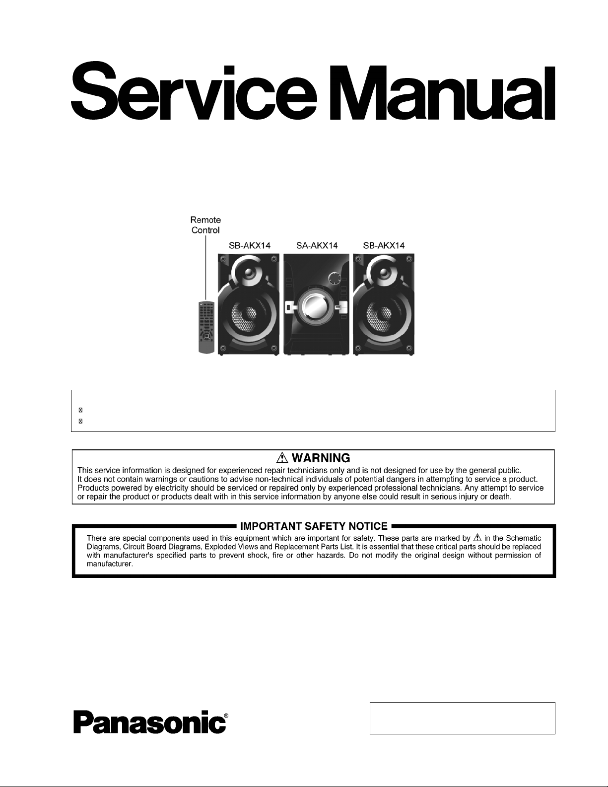
CD Stereo System
Model No. SA-AKX14LM-K
Product Color: (K)...Black Type
Please refer to the original service manual for:
CD Mechanism Unit (BRS1C), Order No. PSG1102001CE
Speaker system SB-AKX14LM-K, Order No. PMX1206002CE
© Panasonic Corporation 2012. All rights reserved.
Unauthorized copying and distribution is a violation
of law.
Page 2

Please refer to the original service manual for:
CD Mechanism Unit (BRS1C), Order No. PSG1102001CE
Speaker system SB-AKX14LM-K, Order No. PMX
1206002CE
Nota: El idioma original de este Manual de Servicio es en idioma inglés, sin embargo algunas notas aquí
mencionadas serán escritas en español para mejor descripción para Centros de Servicio de México.
3 Service Navigation
1 Safety Precautions
1.1. General Guidelines
1.3. Before Repair and Adjustment
1.4. Protection Circuitry
1.5. Caution For Fuse Replacement
1.6. Safety Parts Information
2 Warning
2.1. Prevention of Electrostatic Discharge (ESD)
to Electrostatic Sensitive (ES) Devices
2.2. Precaution of Laser Diode
2.3. Service caution based on Legal restrictions
2.4. Handling Precautions for Traverse Unit
3.1. Service Information
4 Specifications
5 General/Introduction
5.1. Media Information
6 Location of Controls and Components
6.1. Remote Control Key Button Operation
6.2. Main Unit Key Button Operation
7 Installation Instructions
7.1. Speaker and A/C Connection
8 Service Mode
8.1. Cold-Start
8.2. Doctor Mode Table
© Panasonic Corporation 2012. All rights reserved.
Unauthorized copying and distribution is a violation
of law.
2
Page 3

8.3. Reliability Test Mode (CD Mechanism Unit
(BRS1C))
8.4. Self-Diagnostic Mode
8.5. Self-Diagnostic Error Code Table
8.6. Sales Demonstration Lock Function
9 Troubleshooting Guide
9.1. Part Location
9.2. Troubleshooting Guide for F61 and/or F76
9.3. D-Amp IC Operation & Control
10 Service Fixture & Tools
11 Disassembly and Assembly Instructions
11.1. Disassembly Flow Chart
11.2. Main Components and P.C.B. Locations
11.3. Disassembly of Top Cabinet
11.4. Disassembly of Tuner P.C.B.
11.5. Disassembly of Front Panel Unit
11.6. Disassembly of Panel P.C.B.
11.7. Disassembly of Remote Sensor P.C.B.
11.8. Disassembly of USB P.C.B.
11.9. Disassembly of LCD P.C.B.
11.10. Disassembly of CD Lid
11.11. Disassembly of Main P.C.B.
11.12. Replacement of Voltage Regulator Transistor
(Q2022)
11.13. Replacement of Audio Digital Amp IC
(IC5902)
11.14. Disassembly of SMPS P.C.B.
11.15. Replacement of Switching Regulator IC
hh(IC5701)
11.16. Replacement of Rectifier Diode (D5702)
11.17. Replacement of Rectifier Diode (D5801)
11.18. Replacement of Rectifier Diode (D5802)
11.19. Replacement of Regulator Diode (D5803)
11.20. Disassembly of CD Mechanism Unit (BRS1C)
11.21. Disassembly of Rear Panel
18 Printed Circuit Board
18.1. CD Servo P.C.B.
18.2. Main & Tuner P.C.B.
18.3. Panel, LCD, Remote Sensor & USB P.C.B.
18.5. SMPS P.C.B.
19 Appendix Information of Schematic Diagram
19.1. Voltage & Waveform Chart
19.2. Illustration of ICs, Transistor and Diode
19.3. Terminal Function of ICs
20 Exploded View and Replacement Parts List
20.1. Exploded View and Mechanical replacement
Part List
20.2. Electrical Replacement Part List
12 Replacement of Traverse Unit
12.1. Disassembly of Traverse Unit
12.2. Assembly of Traverse Unit
12.3. Disassembly of CD Servo P.C.B.
13 Service Position
13.1. Checking and Repairing of Main P.C.B.
13.2. Checking and Repairing of Panel P.C.B.
13.3. Checking and Repairing of LCD P.C.B.-
13.4. Checking and Repairing of SMPS P.C.B.
13.5. Checking and Repairing of CD Servo P.C.B.-
14 Simplified Block Diagram
14.1. Overall Simplified Block Diagram
14.2. Power Block Diagram
15 Block Diagram
15.1. Servo & System Control
15.2. Audio
15.3. Power Supply
16 Wiring Connection Diagram
17 Schematic Diagram
17.1. Schematic Diagram Notes
17.2. CD Servo Circuit
17.3. Main Circuit
17.4. Panel, LCD, Remote Sensor & USB Circuit
17.5. Tuner
17.6. SMPS Circuit
3
Page 4
1 Safety Precautions
1.1. General Guidelines
1. When servicing, observe the original lead dress. If a short circuit is found, replace all parts which have been overheated or
damaged by the short circuit.
2. After servicing, see to it that all the protective devices such as insulation barriers, insulation papers shields are properly
installed.
3. After servicing, carry out the following leakage current checks to prevent the customer from being exposed to shock hazards.
1.1.1. Leakage Current Cold Check
1. Unplug the AC cord and connect a jumper between the two prongs on the plug.
2. Measure the resistance value, with an ohmmeter, between the jumpered AC plug and each exposed metallic cabinet part on
the equipment such as screwheads, connectors, control shafts, etc. When the exposed metallic part has a return path to the
chassis, the reading should be between 1M and 5.2M .
When the exposed metal does not have a return path to the chassis, the reading must be
1.1.2. Leakage Current Hot Check
1. Plug the AC cord directly into the AC outlet. Do not use an isolation transformer for this check.
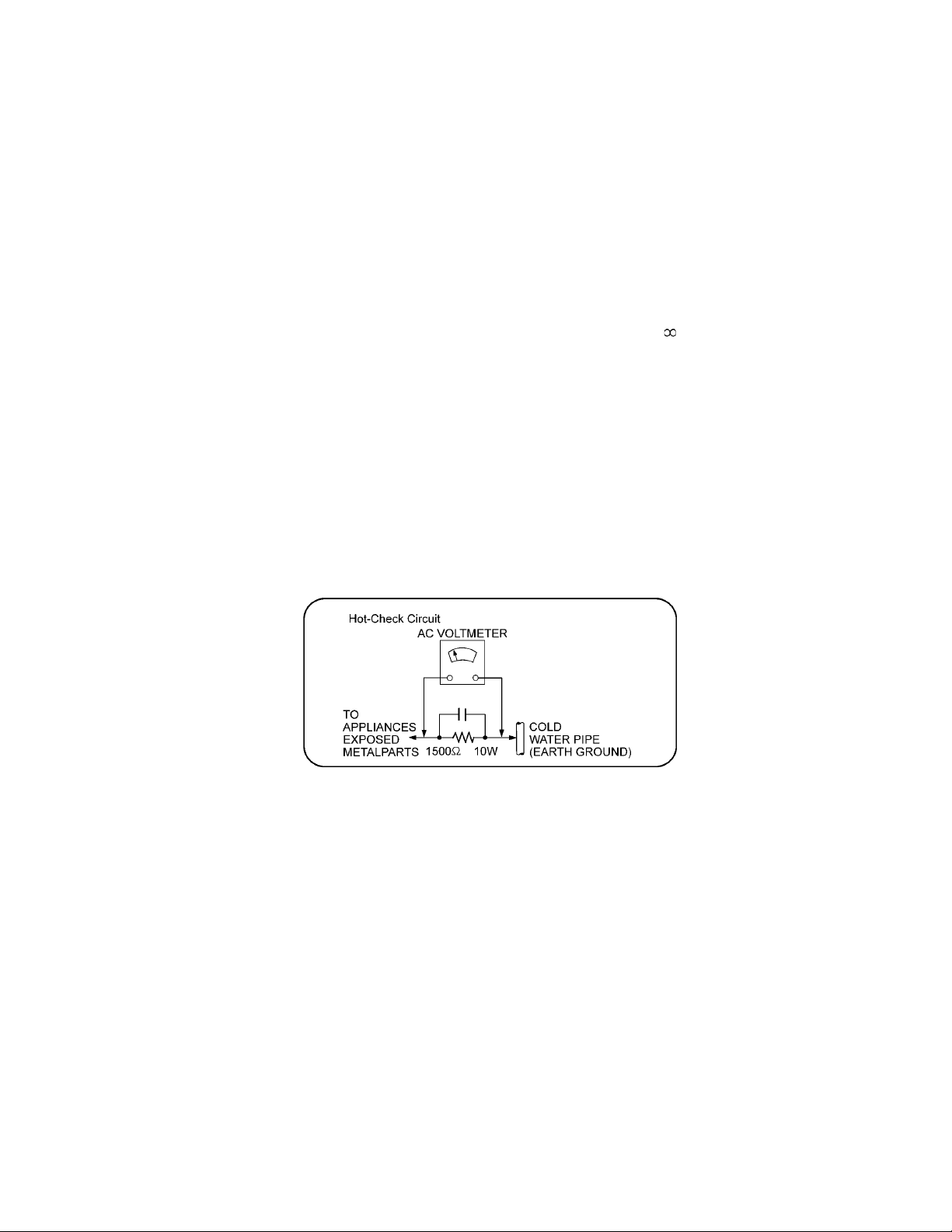
2. Connect a 1.5k , 10 watts resistor, in parallel with a 0.15F capacitors, between each exposed metallic part on the set and a
good earth ground such as a water pipe, as shown in Figure 1.
3. Use an AC voltmeter, with 1000 ohms/volt or more sensitivity, to measure the potential across the resistor.
4. Check each exposed metallic part, and measure the voltage at each point.
5. Reverse the AC plug in the AC outlet and repeat each of the above measurements.
6. The potential at any point should not exceed 0.75 volts RMS. A leakage current tester (Simpson Model 229 or equivalent)
may be used to make the hot checks, leakage current must not exceed 1/2 milliamp. In case a measurement is outside of the
limits specified, there is a possibility of a shock hazard, and the equipment should be repaired and rechecked before it is
returned to the customer.
Figure 1
1.3. Before Repair and Adjustment
Disconnect AC power to discharge unit AC Capacitors as such (C5700, C5701, C5703, C5708)
through a 10 , 10 W resistor to ground.
Caution:
DO NOT SHORT-CIRCUIT DIRECTLY (with a screwdriver blade, for instance), as this may destroy solid state devices.
After repairs are completed, restore power gradually using a variac, to avoid overcurrent.
Current consumption at ~127 V ac /60 Hz in Power ON, FM Tuner, No Signal, volume minimal mode should be
~ 500 mA (PH).
Current consumption at 127 V ac, 60 Hz in Power ON, FM Tuner, No Signal, volume minimal mode should be ~ 500 mA.
4
Page 5
1.4. Protection Circuitry
The protection circuitry may have operated if either of the following conditions are noticed:
s No sound is heard when the power is turned on.
s Sound stops during a performance.
The function of this circuitry is to prevent circuitry damage if, for example, the positive and negative speaker connection wires are
“shorted”, or if speaker systems with an impedance less than the indicated rated impedance of the amplifier are used.
If this occurs, follow the procedure outlines below:
1. Turn off the power.
2. Determine the cause of the problem and correct it.
3. Turn on the power once again after one minute.
Note:
When the protection circuitry functions, the unit will not operate unless the power is first turned off and then on again.
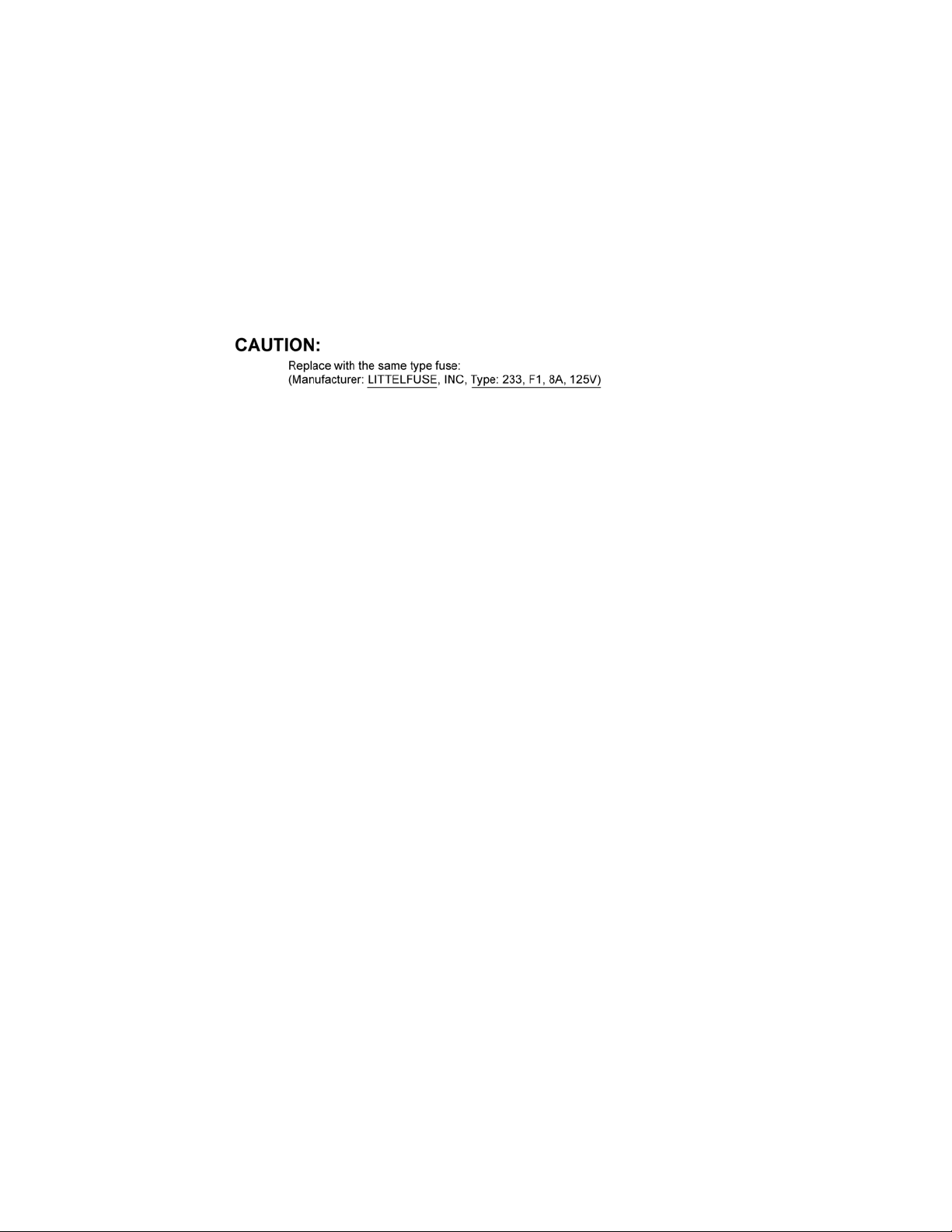
1.5. Caution For Fuse Replacement
5
Page 6
1.6. Safety Parts Information
K
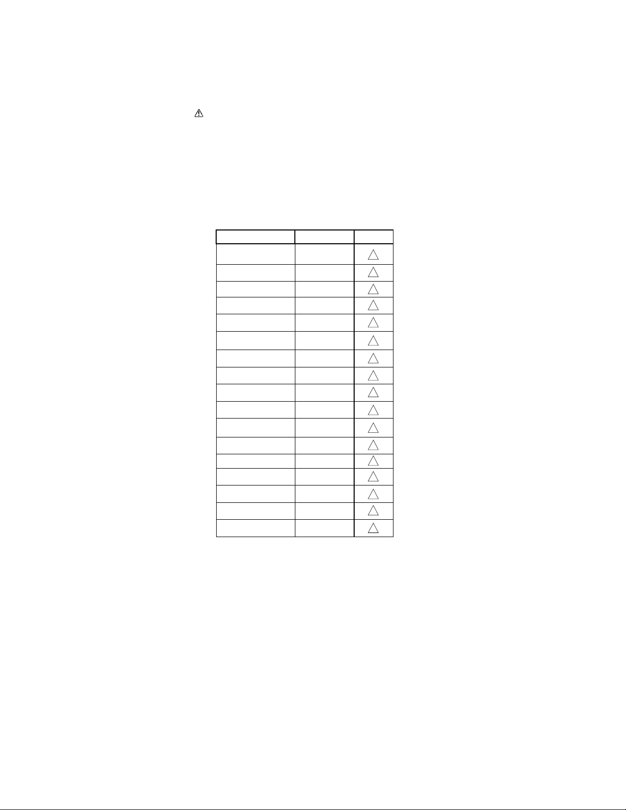
Safety Parts List:
There are special components used in this equipment which are important for safety.
These parts are marked by in the Schematic Diagrams, Exploded View & Replacement Parts List. It is essential that these
critical parts should be replaced with manufacturer’s specified parts to prevent shock, fire or other hazards. Do not modify the
original design without permission of manufacturer.
Modelo:
Nombre del componente
CABLE TOMACORRIENTE.
CONECTOR TOMACORRIENTE
TRANSFORMADOR DE PODER
SC-AKX14LM-
TRANSFORMADOR DE
RESPALDO
FUSIBLE PRIMARIO
ZNR
CAPACITOR DE AC
CAPACITOR DE AC
CAPACITOR DE AC
CAPACITOR DE AC
OPTOACOPLADOR
PCB SMPS
BOBINA PRIMARIO
GAB. MET. SIN DOBLAR
BRS1C CD UNIT
REAR PANEL
INSTRUCTIVO
Numero de Parte Seguridad
K2CB2YY00059
K2AB2B000007
G4DYZ0000057
ETS19AB2E6AG
K5D802APA008
ERZV05Z471CS
F1BAF1020020
F0CAF224A105
F0CAF104A105
F1BAF471A013
B3PBA0000579
RJB3568A-1
G0B612H00004
RKMX1011Z-KL
RD-DDL081-PX
RXTM0002E-A
RQTM0187
!
!
!
!
!
!
!
!
!
!
!
!
!
!
!
!
!
6
Page 7

2 Warning
2.1. Prevention of Electrostatic Discharge (ESD) to Electrostatic Sensitive
(ES) Devices
Some semiconductor (solid state) devices can be damaged easily by static electricity. Such components commonly are called Electrostatically Sensitive (ES) Devices. Examples of typical ES devices are integrated circuits and some field-effect transistors and
semiconductor "chip" components. The following techniques should be used to help reduce the incidence of component damage
caused by electrostatic discharge (ESD).
1. Immediately before handling any semiconductor component or semiconductor-equipped assembly, drain off any ESD on your
body by touching a known earth ground. Alternatively, obtain and wear a commercially available discharging ESD wrist strap,
which should be removed for potential shock reasons prior to applying power to the unit under test.
2. After removing an electrical assembly equipped with ES devices, place the assembly on a conductive surface such as aluminum foil, to prevent electrostatic charge buildup or exposure of the assembly.
3. Use only a grounded-tip soldering iron to solder or unsolder ES devices.
4. Use only an anti-static solder removal device. Some solder removal devices not classified as “anti-static (ESD protected)” can
generate electrical charge sufficient to damage ES devices.
5. Do not use freon-propelled chemicals. These can generate electrical charges sufficient to damage ES devices.
6. Do not remove a replacement ES device from its protective package until immediately before you are ready to install it. (Most
replacement ES devices are packaged with leads electrically shorted together by conductive foam, aluminum foil or comparable conductive material).
7. Immediately before removing the protective material from the leads of a replacement ES device, touch the protective material
to the chassis or circuit assembly into which the device will be installed.
Caution:
Be sure no power is applied to the chassis or circuit, and observe all other safety precautions.
8. Minimize bodily motions when handling unpackaged replacement ES devices. (Otherwise harmless motion such as the
brushing together of your clothes fabric or the lifting of your foot from a carpeted floor can generate static electricity (ESD) suf-
ficient to damage an ES device).
7
Page 8
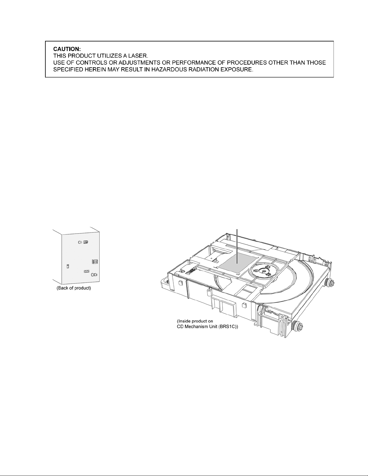
2.2. Precaution of Laser Diode
Caution:
This product utilizes a laser diode with the unit turned “on”, invisible laser radiation is emitted from the pickup lens.
Wavelength: 790 nm (CD)
Maximum output radiation power from pickup: 100 PW/VDE
Laser radiation from the pickup unit is safety level, but be sure the followings:
1. Do not disassemble the pickup unit, since radiation from exposed laser diode is dangerous.
2. Do not adjust the variable resistor on the pickup unit. It was already adjusted.
3. Do not look at the focus lens using optical instruments.
4. Recommend not to look at pickup lens for a long time.
8
Page 9
2.3. Service caution based on Legal restrictions
2.3.1. General description about Lead Free Solder (PbF)
The lead free solder has been used in the mounting process of all electrical components on the printed circuit boards used for this
equipment in considering the globally environmental conservation.
The normal solder is the alloy of tin (Sn) and lead (Pb). On the other hand, the lead free solder is the alloy mainly consists of tin
(Sn), silver (Ag) and Copper (Cu), and the melting point of the lead free solder is higher approx.30 degrees C (86qF) more than that
of the normal solder.
Definition of PCB Lead Free Solder being used
The letter of “PbF” is printed either foil side or components side on the PCB using the lead free solder.
(See right figure)
Service caution for repair work using Lead Free Solder (PbF)
• The lead free solder has to be used when repairing the equipment for which the lead free solder is used.
(Definition: The letter of “PbF” is printed on the PCB using the lead free solder.)
• To put lead free solder, it should be well molten and mixed with the original lead free solder.
• Remove the remaining lead free solder on the PCB cleanly for soldering of the new IC.
• Since the melting point of the lead free solder is higher than that of the normal lead solder, it takes the longer time to melt the
lead free solder.
• Use the soldering iron (more than 70W) equipped with the temperature control after setting the temperature at 350±30 degrees
C (662±86qF).
Recommended Lead Free Solder (Service Parts Route.)
• The following 3 types of lead free solder are available through the service parts route.
RFKZ03D01K-----------(0.3mm 100g Reel)
RFKZ06D01K-----------(0.6mm 100g Reel)
RFKZ10D01K-----------(1.0mm 100g Reel)
Note
* Ingredient: tin (Sn), 96.5%, silver (Ag) 3.0%, Copper (Cu) 0.5%, Cobalt (Co) / Germanium (Ge) 0.1 to 0.3%
9
Page 10
2.4. Handling Precautions for Traverse Unit
The laser diode in the optical pickup unit may break down due to static electricity of clothes or human body. Special care must be
taken avoid caution to electrostatic breakdown when servicing and handling the laser diode in the traverse unit.
2.4.1. Cautions to Be Taken in Handling the Optical Pickup Unit
The laser diode in the optical pickup unit may be damaged due to electrostatic discharge generating from clothes or human body.
Special care must be taken avoid caution to electrostatic discharge damage when servicing the laser diode.
1. Do not give a considerable shock to the optical pickup unit as it has an extremely high-precise structure.
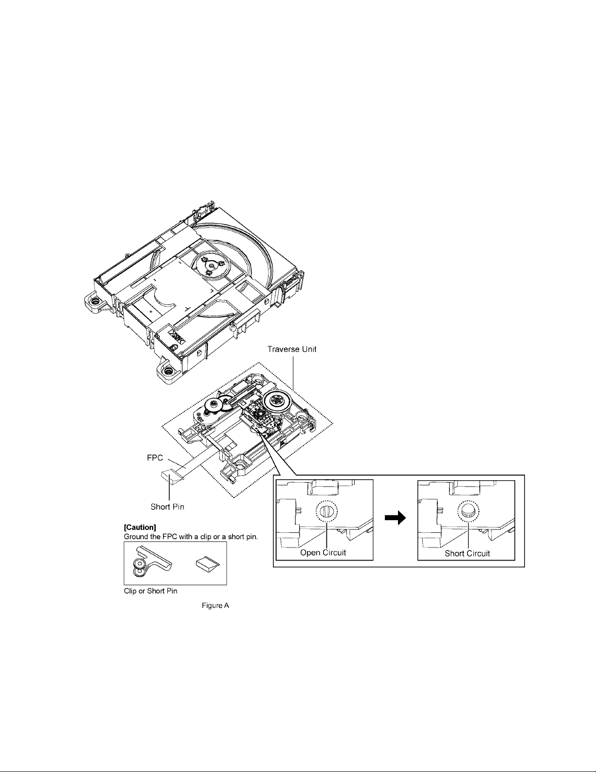
2. To prevent the laser diode from the electrostatic discharge damage, the flexible cable of the optical pickup unit removed
should be short-circuited with a short pin or a clip.
3. The flexible cable may be cut off if an excessive force is applied to it. Use caution when handling the flexible cable.
4. The antistatic FPC is connected to the new optical pickup unit. After replacing the optical pickup unit and connecting the flexible cable, cut off the antistatic FPC.
10
Page 11
2.4.2. Grounding for electrostatic breakdown prevention
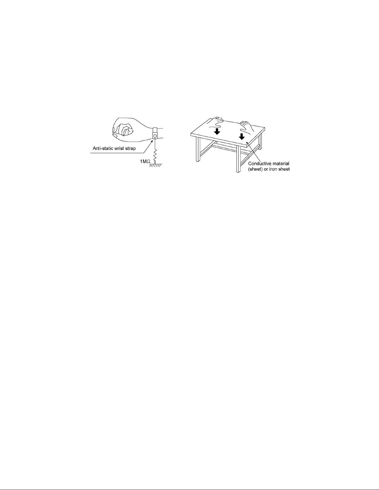
Some devices such as the DVD player use the optical pickup (laser diode) and the optical pickup will be damaged by static electricity in the working environment. Proceed servicing works under the working environment where grounding works is completed.
2.4.2.1. Worktable grounding
1. Put a conductive material (sheet) or iron sheet on the area where the optical pickup is placed, and ground the sheet.
2.4.2.2. Human body grounding
1. Use the anti-static wrist strap to discharge the static electricity form your body.
11
Page 12

3 Service Navigation
3.1. Service Information
This service manual contains technical information which will allow service personnel’s to understand and service this model.
Please place orders using the parts list and not the drawing reference numbers.
If the circuit is changed or modified, this information will be followed by supplement service manual to be filed with original service
manual.
• CD Mechanism Unit (BRS1C):
1) This model uses CD Mechanism Unit (BRS1C).
• Micro-processor:
1) The following components are supplied as an assembled part.
- Micro-processor IC, IC2003 (*MN101EF16KXW) * Este material se encuentra sin programar, necesita ser programado.
• Speaker System:
1) This model uses Speaker System, SB-AKX14LM-K.
12
Page 13

4 Specifications
rodacifilpmalednóicceS
oerétseodomneSMRadilasedaicnetoP
)sodalortnocselanacsobma(latnorflanaC
4(lanacropW521
oerétseodomledSMRlatotaicnetoP
OPMPadilasedaicnetoP
sadarugifnocerpsarosimE
adaludomaicneucerF
)MF(
saicneucerfedamaG
9,78
desbalanceado)(
mreT
adaludomdutilpmA)MA(
saicneucerfedamaG
XUAadartnE
57anetnaaledselani
DHT%01,zHk1,)
Peso
)DHT%01(W052
).xám(W023
W0063
selanimret,rodazinotnislednóicceS
Consumo de energía en modo normal
MFedsarosime03
MAedsarosime51
58Wh/día (considerando 1 hora de uso al día).
Consumo de energía en modo de espera
4,6Wh/día (considerando 23 horas en modo de espera
al día).
)zHk001edsosapne(zHM0,801azHM5,78
)zHk002edsosapne(zHM9,701azHM
)zHk01edsosapne(zHk0171azHk025
ACRkcajajivalC
:atoN
.osiva
El peso y las dimensiones son aproximados.
daL
sedadilareneG
aígreneedomusnoC
nóicatnemilaedetneuF
)frPxlAxnA(senoisnemiD
%53
.latigidortcepse
~
otneimanoicnufedsarutarepmetedamaG
otneimanoicnufedsedademuhedamaG
W85
zH06,V721
mm542xmm433xmm022
k8,2
g
C°04+aC°0
)nóicasnednocnis(avitalerdademuh%08a
oiverpnissoibmacasatejusnátsesenoicacificepsesaL
edrodazilanalenocedimeslatotacinómranóisrotsi
sotcapmocsocsidednóicceS
)mc21omc8(sodicudorpersocsiD
rotceL
)ocsiD(oiduaedadilaS
selanacedoremúN
odreiuqzilatnorflanaC=LF
Ú
3reyaL1-GEPM
ohceredlatnorflanaC=RF
Ú
3PM,AD-DC(WR/R-DC,DC
)
)DC(mn097adnoeddutignoL
1SSALCresáledaicnetoP
)RF,LF(selanac2
Peso
BSUednóicceS
BSUotreuP
latotdadicolev0,2BSUradnátseBSU
soidemedsovihcraedotamrofnocdadilibitapmoC
*
)3pm.
(3PM
BSUovitisopsidedovihcraedametsiS
23TAF,61TAF,21TAF
).xám(Am005BSUotreupaígrenE
3aspbk61stibeddadicoleV
)nóiccudorper(spbk02
baflesednóicceS
opiT
)s(anicoB
aicnadepmI
itsúcanóiserP
adilasedac
saicneucerfedamaG
)frPxlAxnA(senoisnemiD
asív2edasnicob2edametsiS
)sevargsodinosedojelfer(
mc61edocinócopiTsevargarapanicoB
mc6edocinócopiTsodugaarapanicoB
4
)m1(W/Bd58
)Bd61–(zHk22azH84
)Bd01–(zHk02azH25
mm391xmm433xmm002
k5,2
g
13
Page 14
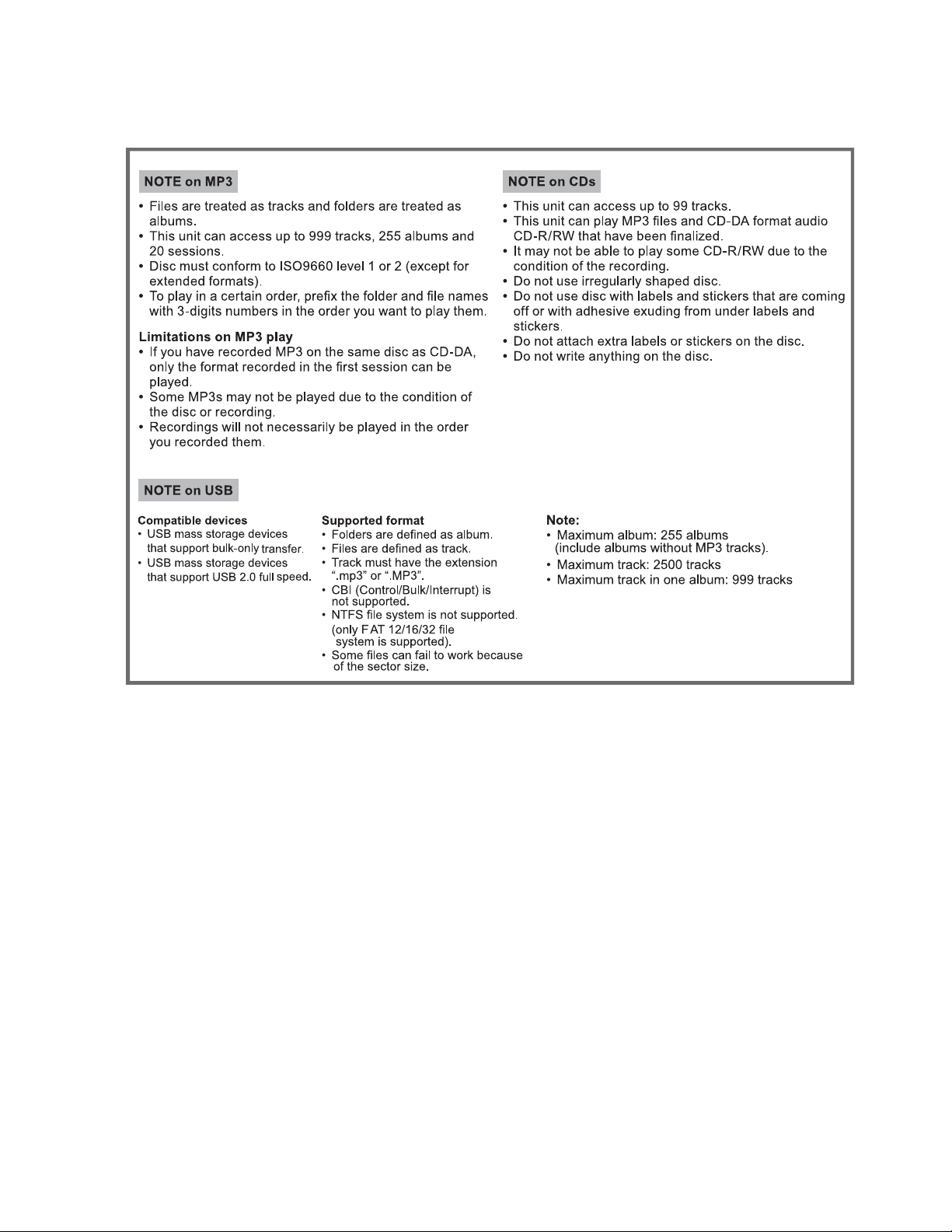
5 General/Introduction
5.1. Media Information
14
Page 15
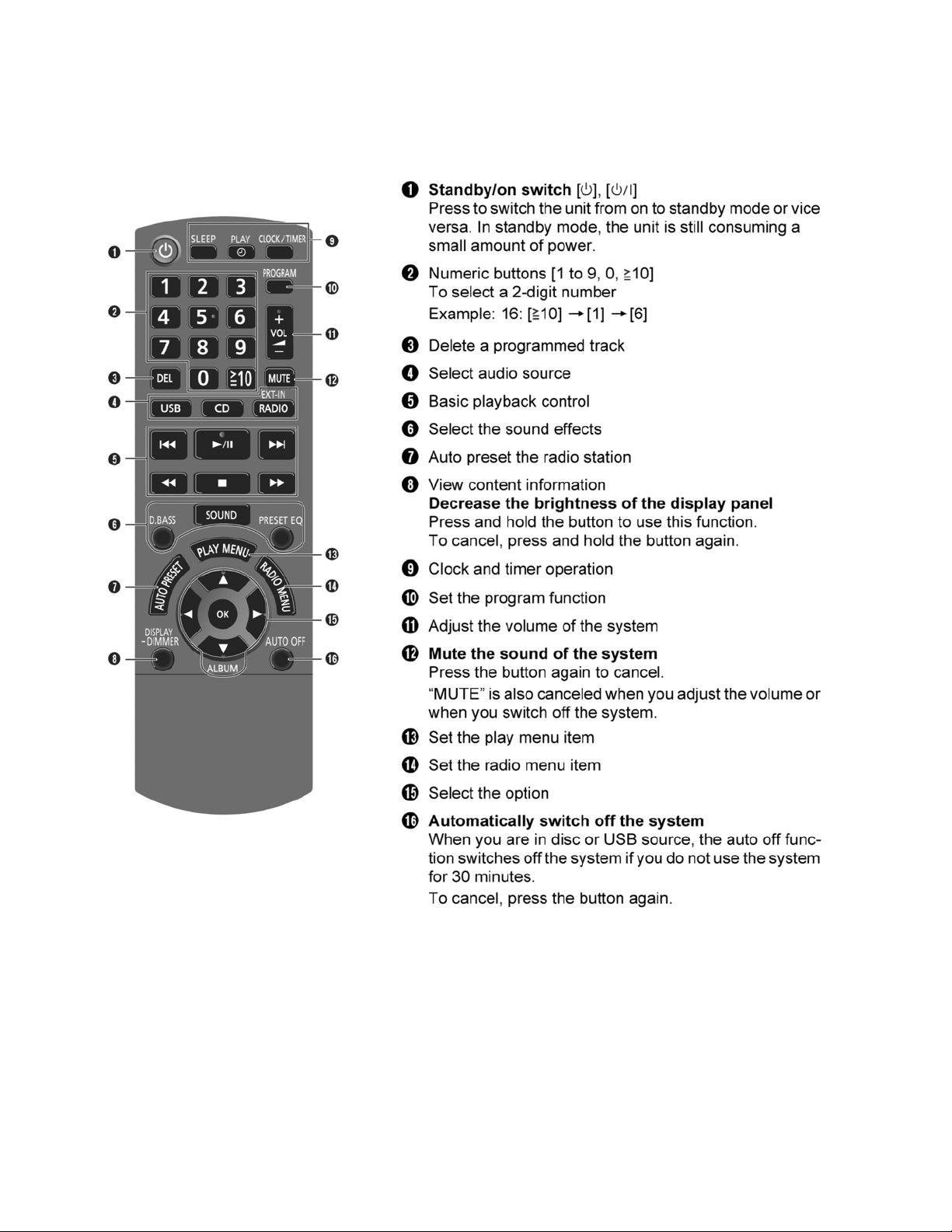
6 Location of Controls and Components
6.1. Remote Control Key Button Operation
15
Page 16
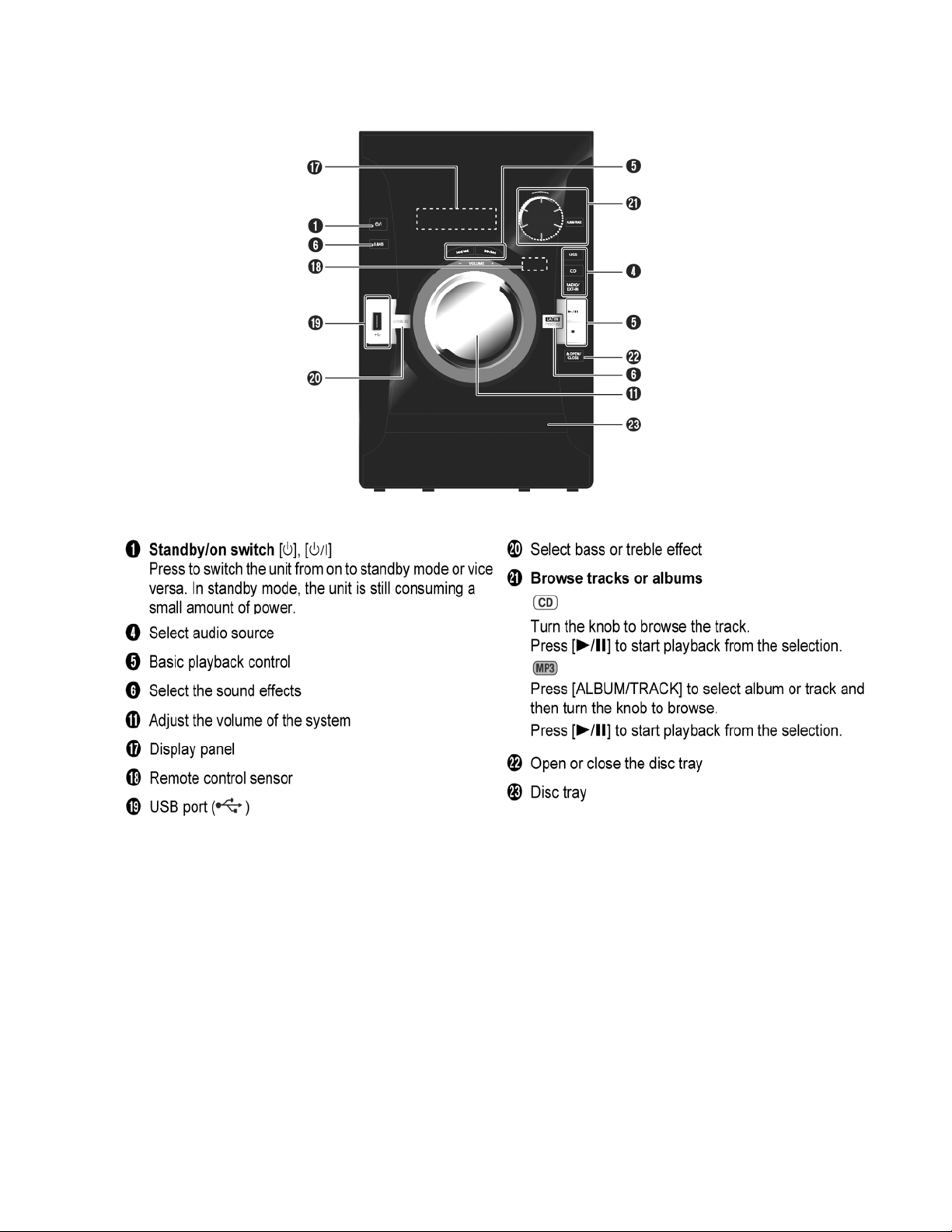
6.2. Main Unit Key Button Operation
16
Page 17
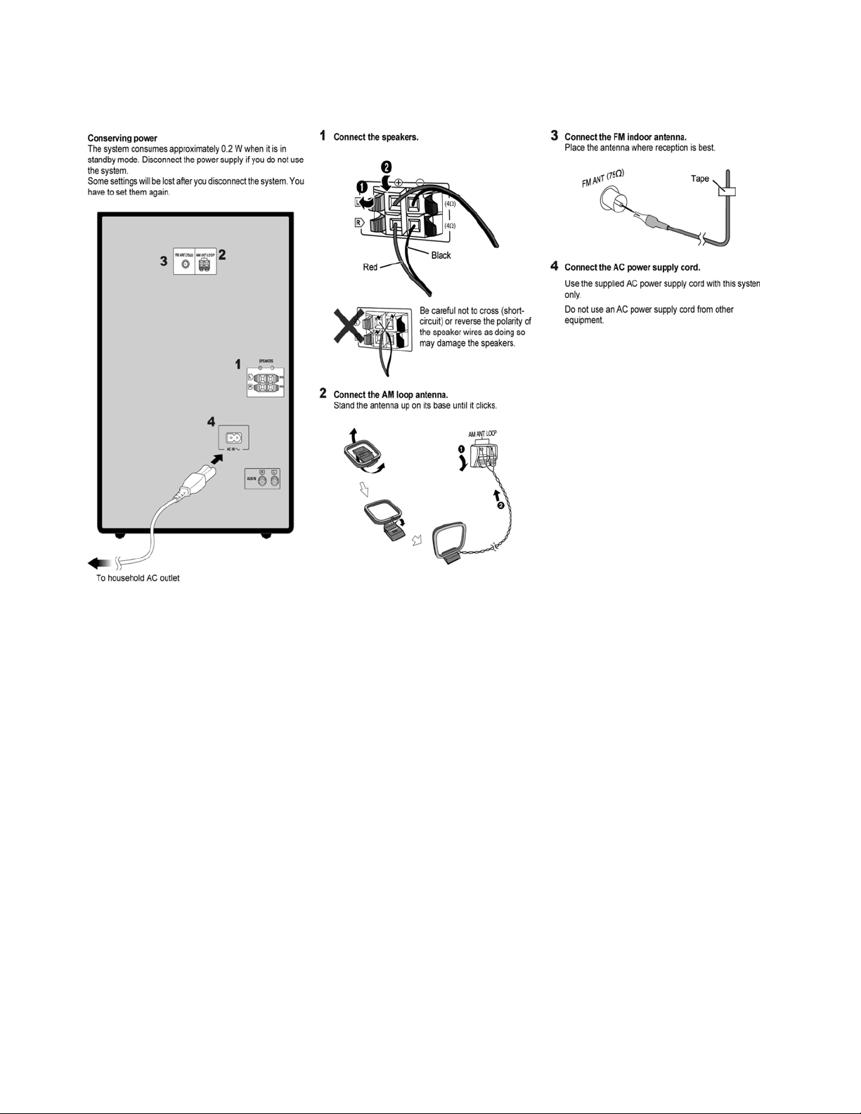
7 Installation Instructions
7.1. Speaker and A/C Connection
17
Page 18

8 Service Mode
8.1. Cold-Start
Here is the procedure to carry out cold-start or initialize to shipping mode.
1. Unplug AC power cord
2. Press & hold [POWER] button
3. Plug AC power cord while [POWER] button being pressed
FL Display will show “_ _ _ _ _ _ _ _”
4. Release [POWER] button
18
Page 19
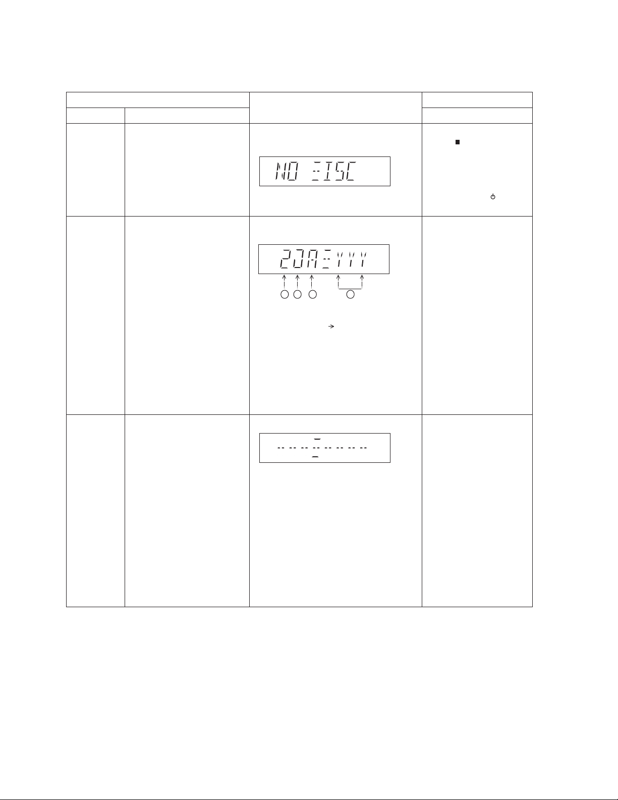
8.2. Doctor Mode Table
8.2.1. Doctor Mode Table 1
Doctor Mode
EEPROM
checksum
check
Item
DescriptionMode Name
To enter into Doctor Mode In CD Mode:
Displaying of
1. Year Develop.
2. Model Type.
3. ROM Type.
4. Firmware Version.
Version No. (001 ~ 999) specific for each firmware
23 41
FL Display
(Decimal)
Key Operation
1. Press [ ] button on
main unit follow by [4]
and [7] on remote
control.
2. To exit, press [DELETE]
button on remote control
or, press [POWER, /I] button
on Main Unit
In CD mode:
1. Enter Doctor Mode
Front Key
Cold Start To active cold start upon next AC
power up when reset start is
execute the next time .
In Doctor Mode :
1. Press [SLEEP] button
on remote control.
19
Page 20
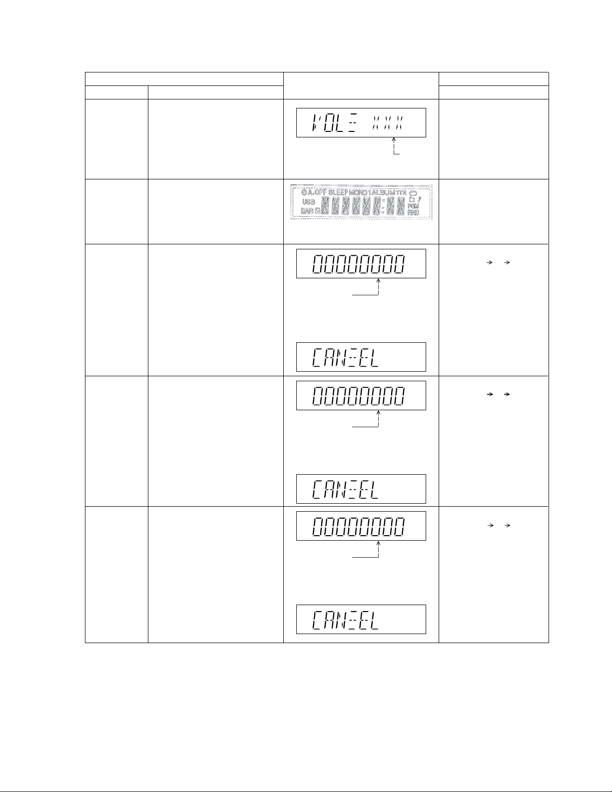
8.2.2. Doctor Mode Table 2
Volume Setting
Check
FL Display
Check
BRS1C Reliability
Test (Traverse)
Item
DescriptionMode Name
To check the volume setting of a main
unit.
To check the FL segment display
All segment will light up while all LED
blink at 0.5s,intervals.(if any)
To determine CD Mechanism BRS1C
Access Inner & Outer disc operation.
In this mode,ensure the CD is in the
main unit.
Note: Refer to Section 6.3 Fig 2. for
process flow.
FL Display
Press [7]: VOL50
Press [8]: VOL35
Press [9]: VOL0
The counter will
increment by one.
When reach 9999
will change to 0000
Cancellation Display
Key Operation
Front Key
In Doctor Mode:
1. Press [7], [8], [9] button
on remote control.
Volume
In Doctor mode:
1. Press [1] button on
remote control.
2. To cancel, press [0]
on remote control.
In Doctor Mode:
1. Press [10] [1] [2] button
on remote control.
2. To cancel, press [0]
on remote control.
BRS1C Reliability
Test
(Combination)
BRS1C Reliability
Test (Loading)
To determine CD Mechanism Unit
(BRS1C) Open/Close & Access Inner &
Outer Disc Operation.
In this mode,ensure the CD is in the
main unit.
Note: Refer to Section 6.3 Fig 3. for
process flow.
To determine CD Mechanism Unit
(BRS1C) Open/Close operation.
In this mode, the tray will open &
close.
Note: Refer to Section 6.3 Fig 1 for
process flow.
In Doctor Mode:
1. Press [10] [1] [5] button
on remote control.
The counter will
increment by one.
When reach 9999
will change to 0000
Cancellation Display
2. To cancel, press [0]
on remote control.
In Doctor Mode:
1. Press [10] [2] [1] button
on remote control.
The counter will
increment by one.
When reach 9999
will change to 0000
Cancellation Display
2. To cancel, press [0]
on remote control.
20
Page 21
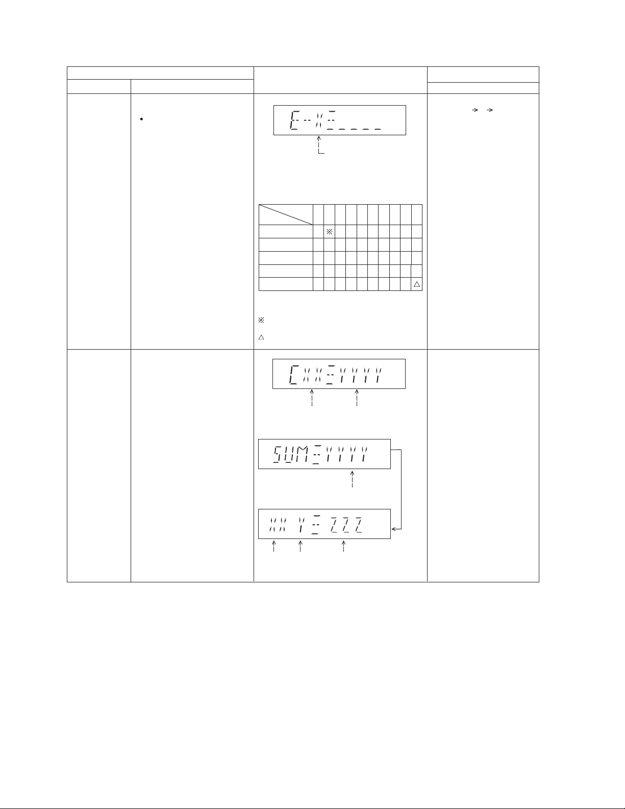
8.2.3. Doctor Mode Table 3
CD
Self- Adjustment
(AJST)
Result Display
CD LSI
Version Check
Item
DescriptionMode Name
i. Function: To display result of
self-adjustment for CD .
This is used for servicing
and analysis.
For checking CD LSI Version and
checksum information.
FL Display
Display of auto
adjustment result
Reference table:
ERROR Code
Status
Condition
012468 ACEF
AOC1/AOC2 O O OOOOOO -
ABC2/ABC1 O - XOXOXO X -
nd
AOC1 O - O X X O O X X -
2
FAGC/T AGC O - O O O XXXX -
AGC2 O - OOOOOO O
O: OK ;
X: NG (In case that time out happens.)
: Either one of FO AOC, TR AOC and
FO coarse AGC is NG .
: If the AGC is NG (ignore others).
Key Operation
Front Key
In Doctor Mode:
1. Press [10] [1] [4] button
on remote control .
2.To cancel, press [0]
on remote control .
In Doctor Mode :
1. Press [4] button
on remote control .
Version (Decimal) Checksum (Hex)
(Display 1)
ROM Version
(Display 2)
Year
Year
Develop
Develop
ROM
Type
Version (Decimal)
2.To cancel, press [0]
on remote control .
after
2 sec
21
Page 22
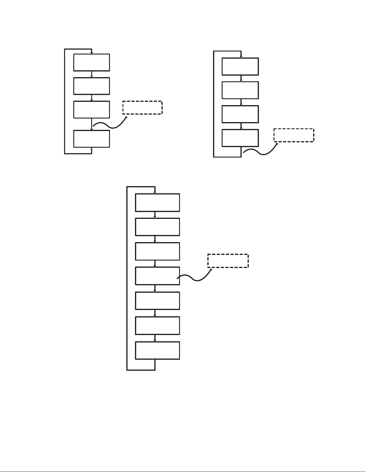
8.3. Reliability Test Mode (CD Mechanism Unit (BRS1C))
Below is the process flow chart of the aging test for the CD Mechanism Unit (BRS1C).
OPEN
Operation
OPEN wait
for 1 s
CLOSE
Operation
CLOSE wait
for 4 s
Fig. 1. Reliability Test (Loading)
Count up
First Track
Access
First Track
Play 10 s
First Track
Access
First Track
Play 5 s
Last Track
Access
Last Track
Play 5 s
Fig. 2. Reliability Test (Traverse)
Count up
Last Track
Access
Last Track
Play 10 s
Open
Operation
Open wait
for 1 s
CLOSE
Operation
Fig. 3. Reliability Test (Combination)
Count up
22
Page 23
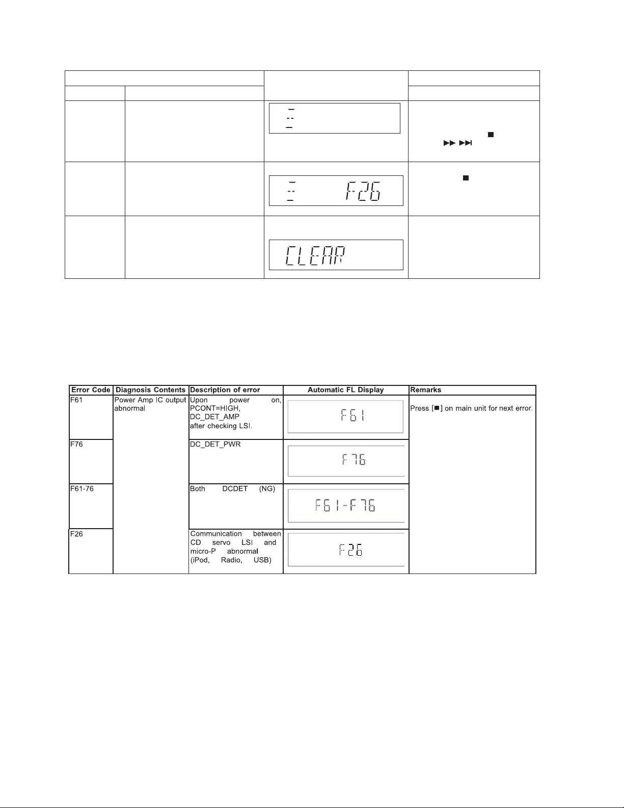
8.4. Self-Diagnostic Mode
Mode Name
Self Diagnostic
Mode
Error code
information
Delete error
code
Item
Description
To enter into self diagnostic checking
System will perform a check on any
unusual/error code from the memory
To clear the stored in memory
(EEPROM IC)
Example:
FL Display
Step 1: Select CD mode
(Ensure no disc is inserted).
Step 2: Press & hold [ ] follow by
[
seconds.
Step 1: In self diagnostic mode,
Press [ ] on main unit.
To exit, press [^/I] on main
unit or remote control.
Step 1: In self diagnostic mode,
Press [0] on remote control.
To exit, press [^/I] on main
unit or remote control.
Key Operation
Front Key
/
] on main unit for 2
8.5. Self-Diagnostic Error Code Table
Self-Diagnostic Function (Refer Section 6.4. Self-Diagnostic Mode) provides information on any problems occurring for the unit and
its respective components by displaying the error codes. These error code such as U**, H** and F** are stored in memory and held
unless it is cleared.
The error code is automatically display after entering into self-diagnostic mode.
8.5.1. Power Supply Error Code Table
23
Page 24
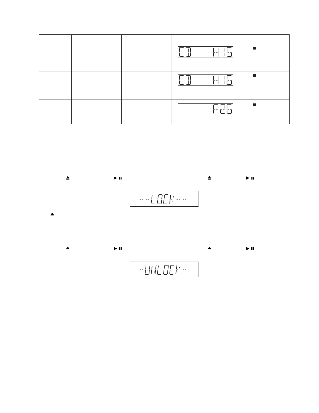
8.5.2. CD Mechanism Error Code Table (CD Mechanism Unit (BRS1C))
Error Code Diagnostic Contents Description of error Automatic FL Display Remarks
CD H15 CD Open Abnormal During operation
POS_SW_R On fail to be
detected with 4 sec. Error
No. shall be clear by force
or during cold start.
CD H16 CD Closing Abnormal During operation
POS_SW_CEN On fail to
be detected with 4 sec.
Error No. shall be clear by
force or during cold start.
Press [
next error.
Press [
next error.
] on main unit for
] on main unit for
F26 Communication between
CD servo LSI and micro-p
abnormal.
During switch to CD function, if SENSE = “L” within
failsafe time of 20ms.
8.6. Sales Demonstration Lock Function
8.6.1. Entering into sales Demo Mode
Here is the procedures to enter into Sales Demonstration Lock.
Step 1: Turn on the unit.
Step 2: Select to any mode function.
Step 3: Press [
Step 4: The display will show upon entering into this mode for 2 sec..
Note: [
8.6.2. Cancellation
Step 1: Turn on the unit.
Step 2: Select to any mode function.
Step 3: Press [
Step 4: The display will show upon entering into this mode for 2 sec..
OPEN/CLOSE] key then [ / ] key at the same time,press and hold both [ OPEN/CLOSE] and [ / ] keys for 5 sec.
OPEN/CLOSE] button is invalid and the main unit displays “LOCKED” while the lock function mode is entered.
OPEN/CLOSE] key then [ / ] key at the same time,press and hold both [ OPEN/CLOSE] and [ / ] keys for 5 sec.
Press [
next error.
] on main unit for
24
Page 25
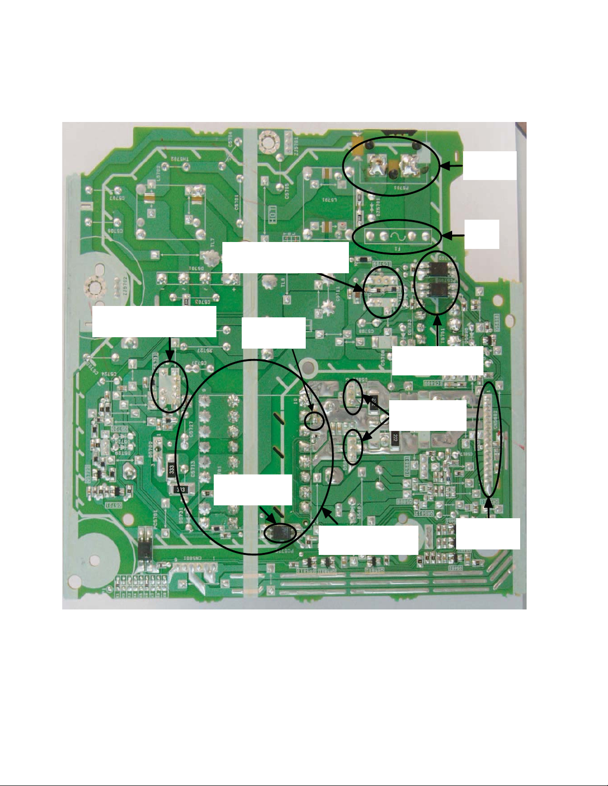
9 Troubleshooting Guide
9.1. Part Location
9.1.1. SMPS P.C.B.
SMPS Control IC:
IC5799
Switching Regulator IC:
IC5701
Thermistor:
TH5860
AC Inlet:
P5701
Fuse:
F1
Photocoupler:
PC5702, PC5799
Photocoupler:
PC5720
Fig. 1 SMPS P.C.B.
Rectifier Diode
D5801, D5802
Main Transformer:
T5701
Connector:
CN5802
25
Page 26
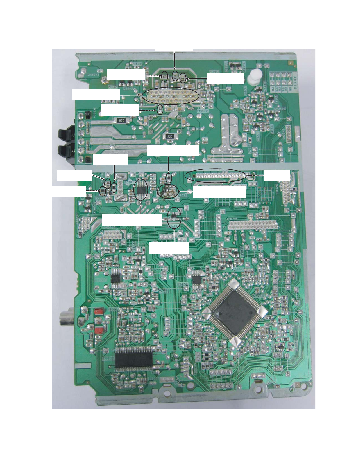
9.1.2. Main P.C.B.
Resistor Defective
R5905
Audio Digital
IC5902
Regulator Circuit
D2017
Regulator Circuit
Q2000
Resistor Defective
R5936
Amp IC
Resistor Defective
R5926
Regulator Circuit
Q2022
Switching Voltage Regulator
IC2011
Resistor Defective
R5928
Voltage Regulator Circuit
D2004
Cable Wire
CN2000
Voltage Regulator Circuit
IC2021
Voltage Regulator
IC2009
Fig. 2 Main P.C.B.
26
Page 27
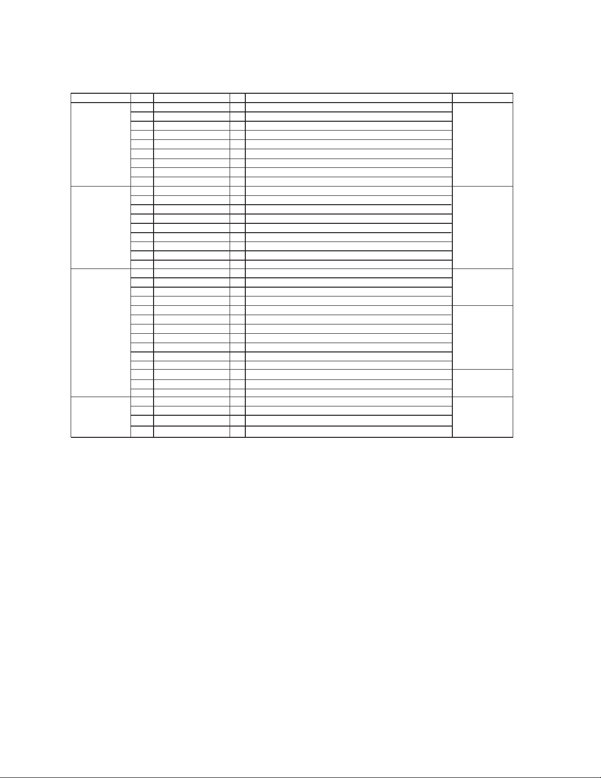
9.2. Troubleshooting Guide for F61 and/or F76
This section illustrates the checking procedures when upon detecting the error of “F61” and/or “F76” after power up of the unit. It is
for purpose of troubleshooting and checking in SMPS & Main P.C.B.
Symptom Remarks
Set cannot ON 1 AC Cord 1 AC Cord Faulty, Loose connection.
Set can ON
then F6 1
Set can ON
then F7 6
Set can ON
working normally
for some time
then F7 6
2
AC Inlet, P5701 P5701 solder crack, dry joint.
3 F use, F1 3 Fuse, F1 Open.
4 P hotocoupler 4 PC5702/PC5799 solder crack.
PC5702, PC5799 Dry joint, short circuit, open circuit.
5 S witching Regulator 5 IC5701 Faulty.
IC, IC5701
6 V oltage Regulator
Transistor (Q2022)
1 S peaker Output 1 Faulty speaker unit, Loose connection, Short.
2 D -AMP circuit D-AMP IC, IC5902 defective.
1 Main Transformer T5701 Short circuit between Pin 14 and Pin 15.
2 DC-DC Circuit 2a
3 P hotocoupler
PC5720
1 R ecti•er Diode D580 Improper contact between D5801 to Heatsink.
Recti•er Diode D5802 Improper contact between D5802 to Heatsink.
2 T hermistor TH5860 1b Set trigger temperature protection.
2
6 Q2022 Faulty.
2a
(Check DC voltage at speaker terminals, 3V and above defective)
2b
DC Voltage ok but no sound, check DC Voltage at Pin 1.
5V ok condition, 2.5V or 0V defective.
2c
2a, 2b ok but no sound, check PWM waveform at Pin 10 and Pin 14 .
If no PWM, 4 resistors defective (R5905, R5926, R5936, R5928).
1a
1b Short circuit between Pin 15 and Pin 16.
1c Short circuit between Pin 16 and Pin 17.
Check cable wire connection between cable wire CN2000.
(At Main P.C.B) & connector CN5802 (At SMPS P.C.B)
(i) +5V Switching Voltage Regulator (IC2011).
2b
(ii) +3.3V Voltage Regulator (IC2009).
(iii) +9V Voltage Regulator Circuit (Q2021, D2004).
(iv) CD +7.5V Regulator Circuit (Q2000, Q2022, D2017).
3
PC5720 solder crack,
Dry joint, short circuit, open circuit.
1a
Possible Fault(s)Checking Items
Refer to
Section 9.1.1
Fig. 1. SMPS
P.C.B.
Refer to
Section 9.1.2
Fig. 2. Main P.C.B.
Refer to
Section 9.1.1
Fig. 1. SMPS
P.C.B.
Refer to
Section 9.1.2
Fig. 2. Main P.C.B.
Refer to
Section 9.1.1
Fig. 1. SMPS P.C.B.
Refer to Section
9.2.1 Fig. 1. SMPS
P.C.B.
27
Page 28
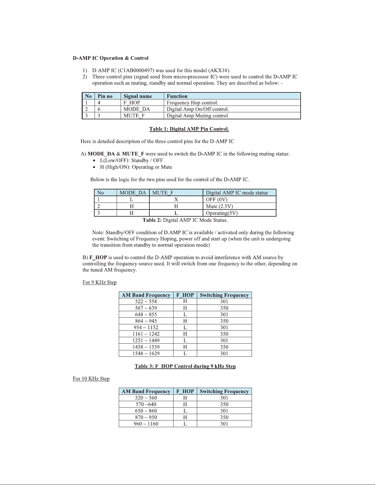
.3. D-Amp IC Operation & Control
28
Page 29

1170 ~ 1250 H 350
1260 ~ 1450 L 301
1460 ~ 1540 H 350
1550 ~ 1710 L 301
Table 4: F_HOP Control during 10 kHz Step
Note: During activating, the 3 control pins namely MUTE_F, MUTE_A and MODE_DA must
be used to cover the “Pop” sound cause by F-HOP switching.
29
Page 30

10 Service Fixture & Tools
Prepare service tools before process service position.
Ref. No Service Tools Remarks
SFT1 Main P.C.B. (CN2000) - SMPS P.C.B. (CN5802) REX1534(15P Cable Wire)
30
Page 31
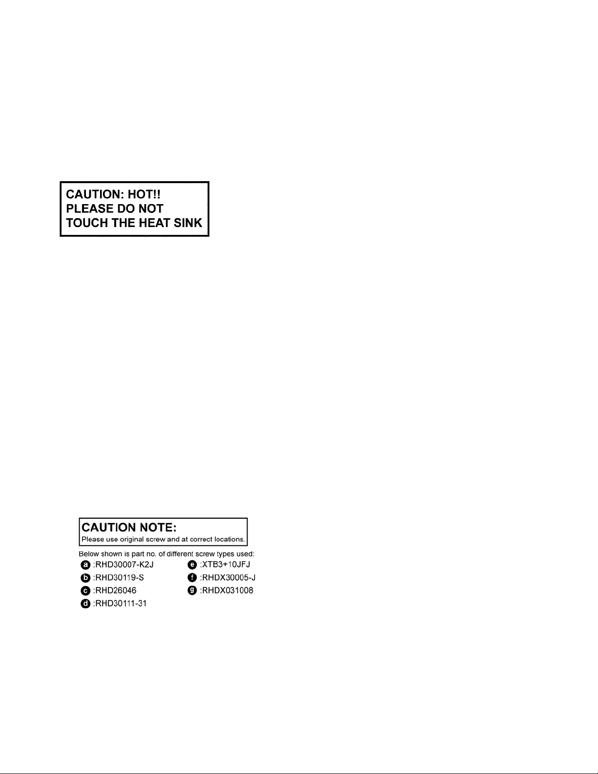
11 Disassembly and Assembly Instructions
• Illustration is based on SA-AKX14PH-K.
Caution Note:
•This section describes the disassembly and/or assembly procedures for all major printed circuit boards & main compo-
nents for the unit. (You may refer to the section of “Main components and P.C.B Locations” as described in the service
manual)
• Before carrying out the disassembly process, please ensure all the safety precautions & procedures are followed.
•During the disassembly and/or assembly process, please handle with care as there may be chassis components with
sharp edges.
•Avoid touching heatsinks due to its high temperature after prolong use. (See caution as described below)
•During disassembly and assembly, please ensure proper service tools, equipments or ji
•During replacement of component parts, please refer to the section of “Replacement Parts List” as described in the ser-
vice manual.
• Select items from the following indexes when disassembly or replacement are required.
• Disassembly of Top Cabinet
• Disassembly of Tuner P.C.B.
• Disassembly of Front Panel Unit
• Disassembly of Panel P.C.B.
• Disassembly of Remote Sensor P.C.B.
• Disassembly of USB P.C.B.
• Disassembly of LCD P.C.B.
• Disassembly of CD Lid
• Disassembly of Main P.C.B.
• Replacement of Voltage Regulator Transistor (Q2022)
• Replacement of Audio Digital Amp IC (IC5902)
• Disassembly of SMPS P.C.B.
• Replacement of Switching Regulator IC (IC5701)
• Replacement of Rectifier Diode (D5702)
• Replacement of Rectifier Diode (D5801)
• Replacement of Rectifier Diode (D5802)
• Replacement of Rectifier Diode (D5803)
• Disassembly of CD Mechanism Unit (BRS1C)
• Disassembly of Rear Panel
• Disassembly of Voltage Selector P.C.B.
gs is being used.
31
Page 32
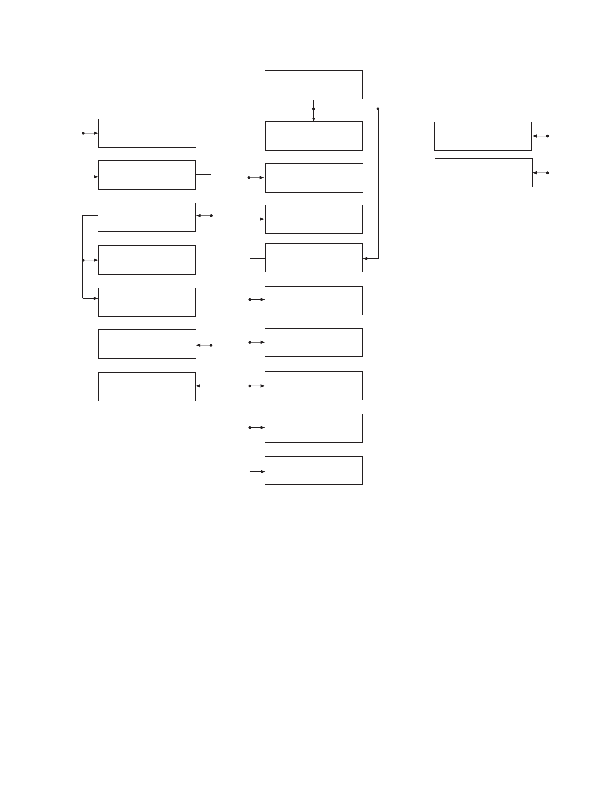
11.1. Disassembly Flow Chart
11.4.
Tuner P.C.B.
11.11.
11.3.
Top Cabinet
Main P.C.B.
11.20.
CD Mechanism Unit
(BRS1C)
11.5.
Front panel Unit
11.6.
Panel P.C.B.
11.7.
Remote Sensor
P.C.B.
11.8.
USB P.C.B.
11.9.
LCD P.C.B.
11.10.
CD Lid
11.12.
Voltage Regulator
Transistor (Q2022)
11.13.
Audio Digital Amp
IC (IC5902)
11.14.
SMPS P.C.B.
11.15.
Switching Regulator
IC (IC5701)
11.16.
Rectifier Diode
(D5702)
11.17.
Rectifier Diode
(D5801)
11.18.
Rectifier Diode
(D5802)
11.21.
Rear Panel
11.22.
Voltage Selector
P.C.B.
11.19.
Rectifier Diode
(D5803)
32
Page 33
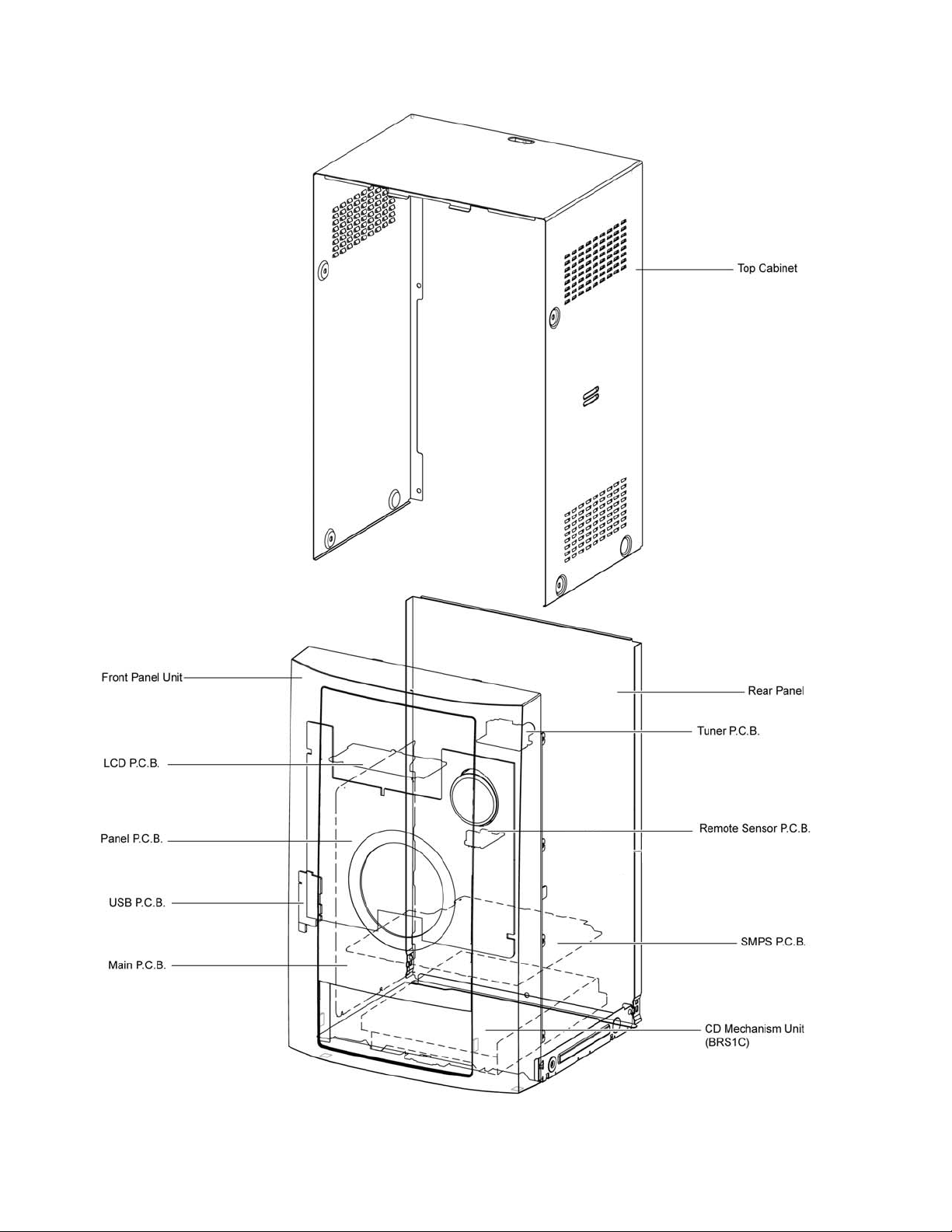
11.2. Main Components and P.C.B. Locations
33
Page 34
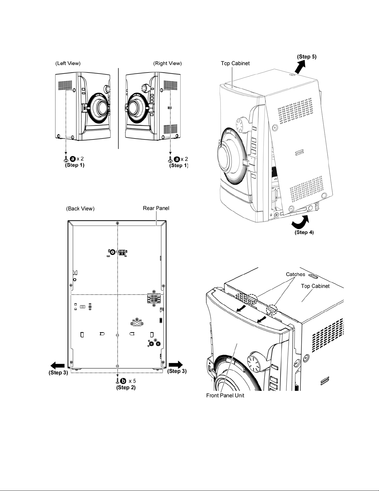
11.3. Disassembly of Top Cabinet
Step 1 Remove 2 screws on each side.
Step 2 Remove 5 screws.
Step 3 Slightly pull both side of Top Cabinet outwards as arrow
shown.
Step 4 Slightly lift up both side of Top Cabinet in an outward
direction as shown.
Step 5 Remove the Top Cabinet.
Caution: During assembling, ensure that the Top Cabinet
catches are properly located into Front Panel Unit as
shown.
34
Page 35
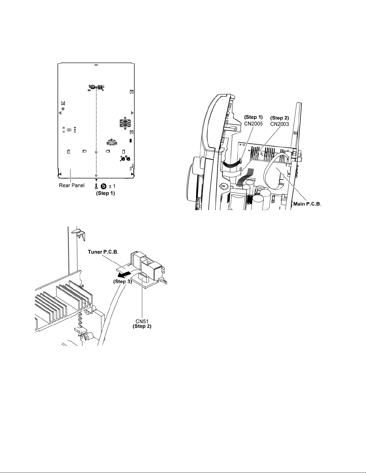
11.4. Disassembly of Tuner P.C.B.
• Refer to “Disassembly of Top Cabinet”.
Step 1 Remove 1 screw.
11.5. Disassembly of Front Panel
Unit
• Refer to “Disassembly of Top Cabinet”.
Step 1 Detach 5P Cable Wire at the connector (CN2005) on
Main P.C.B.
Step 2 Detach 17P FFC at the connector (CN2003) on Main
P. C .B .
Step 2 Detach 9P FFC at the connector (CN51) on Tuner
P.C.B..
Step 3 Remove the Tuner P.C.B..
35
Page 36
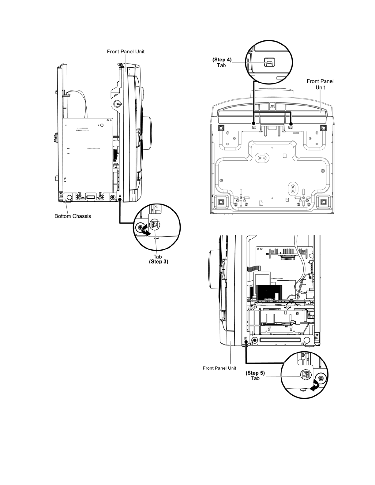
Step 3 Push inwards slightly at the Bottom Chassis as arrow
shown and release tab at left side of Front Panel Unit.
Step 4 Release tabs at bottom.
Step 5 Push inwards slightly at the Bottom Chassis and release
tab at right side of Front Panel Unit.
36
Page 37
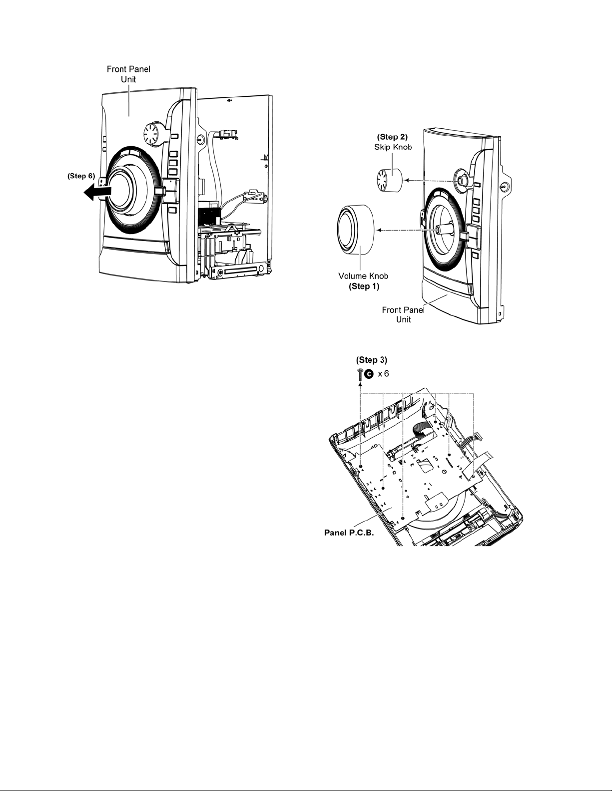
Step 6 Remove the Front Panel Unit
11.6. Disassembly of Panel P.C.B.
• Refer to “Disassembly of Top Cabinet”.
• Refer to “Disassembly of Front Panel Unit”.
Step 1 Remove the Volume Knob.
Step 2 Remove the Skip Knob.
Step 3 Remove 6 screws.
37
Page 38
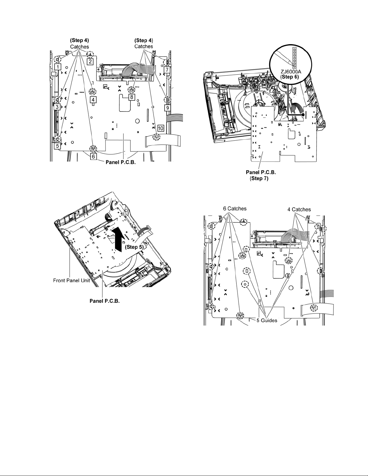
Step 4 Release catches by following the sequences (1-10).
Step 5 Lift up to remove the Panel P.C.B. from Front Panel
Unit.
Step 6 Desolder 7 pins at (ZJ600A) on Panel P.C.B..
Step 7 Remove the Panel P.C.B..
Caution: During assembling, ensure that Panel P.C.B. is
seated properly through the guides & fully catched.
38
Page 39
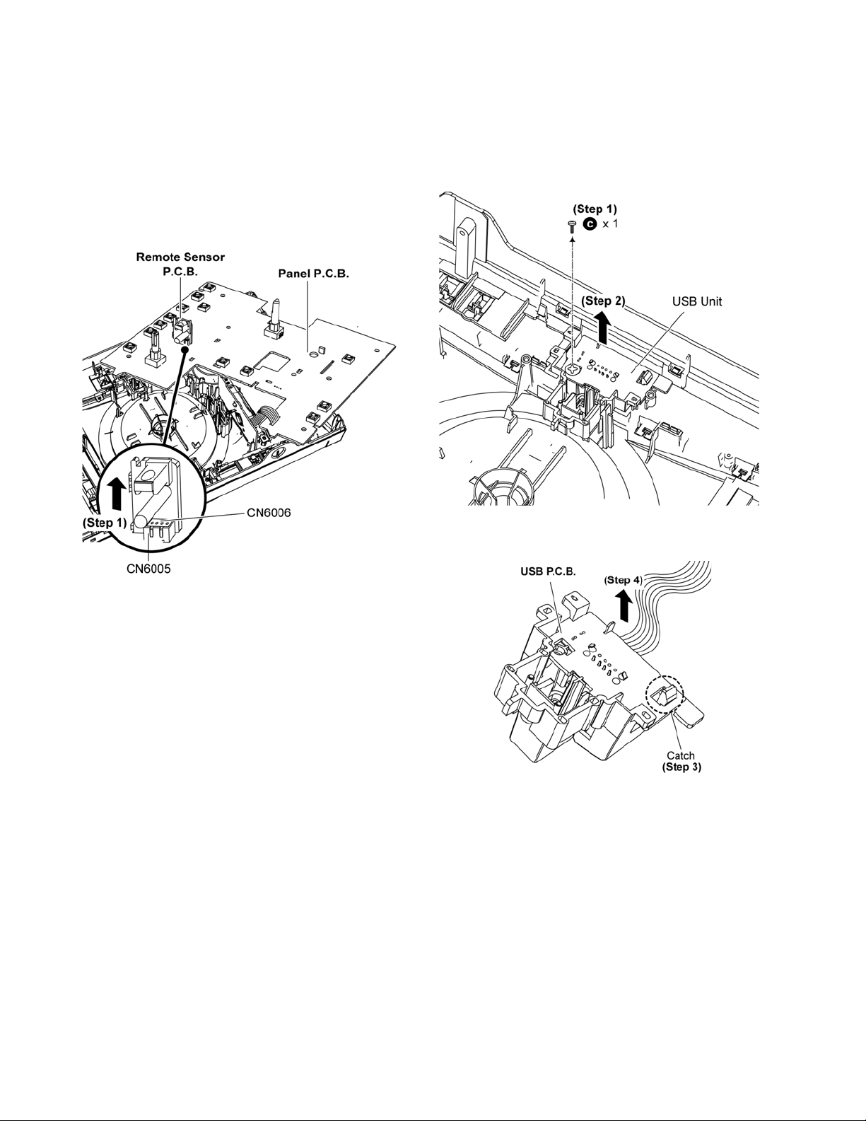
11.7. Disassembly of Remote Sensor
P.C.B.
• Refer to “Disassembly of Top Cabinet”.
• Refer to “Disassembly of Front Panel Unit”.
• Refer to (Step 1) to (Step 5) of item 11.6.
Step 1 Remove the Remote Sensor P.C.B..
Caution: During assembling, ensure that Remote Sensor
P.C.B. is properly inserted & fully connected to Panel
P.C.B..
11.8. Disassembly of USB P.C.B.
• Refer to “Disassembly of Top Cabinet”.
• Refer to “Disassembly of Front Panel Unit”.
• Refer to (Step1) to (Step5) of item 11.6.
Step 1 Remove 1 screw.
Step 2 Remove the USB Unit.
Step 3 Release 1 catch.
Step 4 Remove the USB P.C.B..
39
Page 40
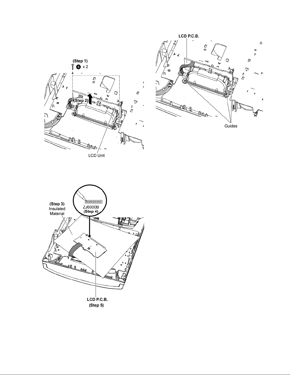
11.9. Disassembly of LCD P.C.B.
• Refer to “Disassembly of Top Cabinet”.
• Refer to “Disassembly of Front Panel Unit”.
Step 1 Remove 2 screws.
Step 2 Lift up the LCD Unit.
Caution: During assembling, ensure that LCD Unit is properly located & seated onto the guides.
Step 3 Place the LCD P.C.B. on an insulated material.
Step 4 Desolder 7 pins (ZJ6000B) on LCD P.C.B..
Step 5 Remove the LCD P.C.B..
40
Page 41
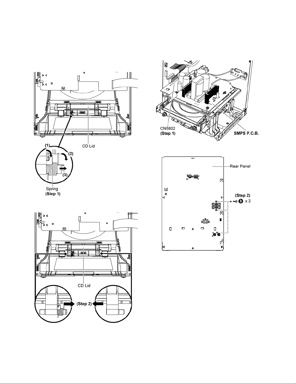
11.10. Disassembly of CD Lid
• Refer to “Disassembly of Top Cabinet”.
• Refer to “Disassembly of Front Panel Unit”.
11.11. Disassembly of Main P.C.B.
• Refer to “Disassembly of Top Cabinet”.
• Refer to “Disassembly of Front Panel Unit”.
Step 1 Remove the spring as arrow shown in order of
sequence (1) to (3).
Caution: During assembling, ensure that the spring is
assembly at correct position.
Step 1 Detach 15P Cable Wire at the connector (CN5802) on
SMPS P.C.B..
Step 2 Remove 3 screws.
Step 2 Remove CD Lid as arrow shown.
41
Page 42
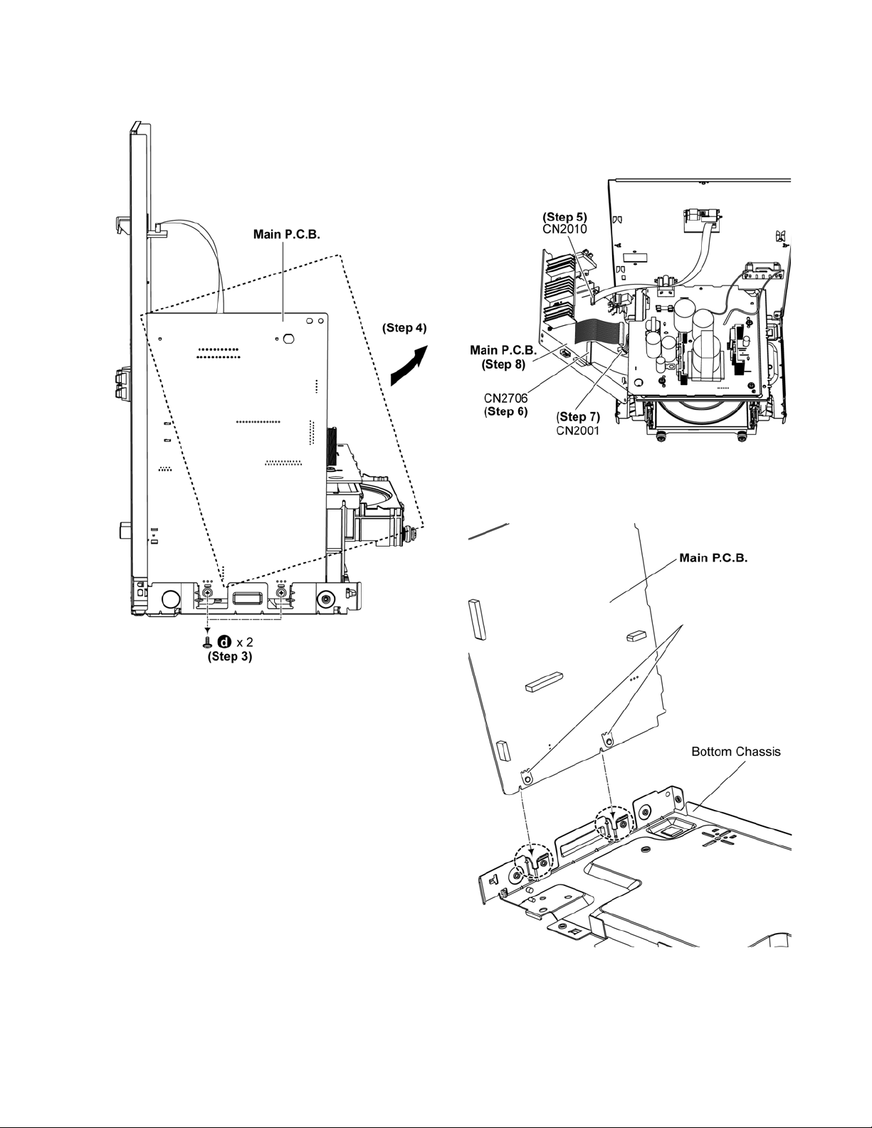
Step 3 Remove 2 screws.
Step 4 Detach Main P.C.B. from Rear Panel according to arrow
shown.
Step 5 Detach 9P FFC at the connector (CN2010) on Main
P. C . B . .
Step 6 Detach 27P FFC at the connector (CN2706) on Main
P. C . B . .
Step 7 Detach 5P Wire (CN2001) in Main P.C.B..
Step 8 Remove Main P.C.B..
Caution: During assembling, ensure that earth plate is
bended flat against the Main P.C.B. properly when inserted
to locators.
42
Page 43
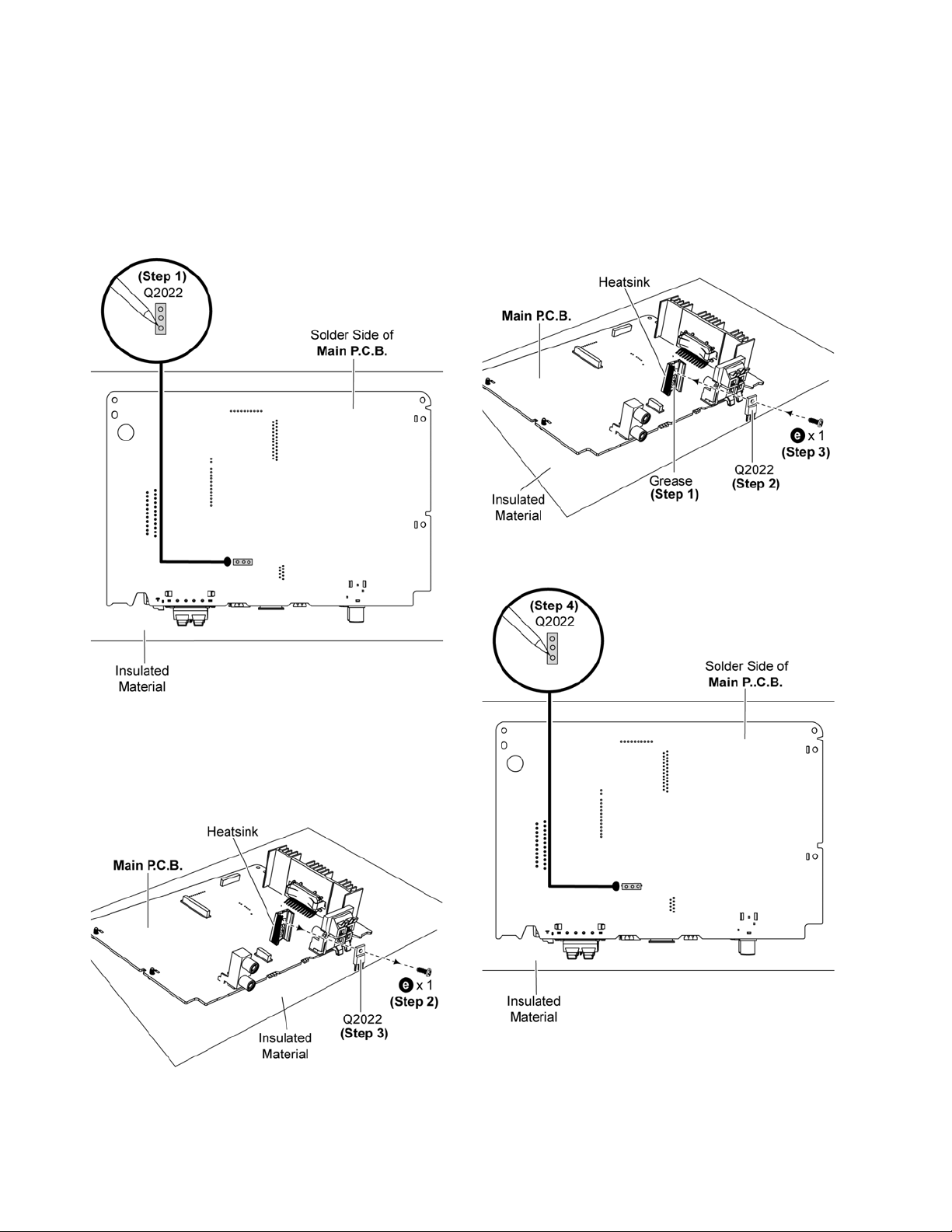
11.12. Replacement of Voltage Regulator Transistor (Q2022)
• Refer to “Disassembly of Main P.C.B.”.
11.12.1. Disassembly of Voltage Regulator
Transistor (Q2022)
Step 1 Desolder pins of the Voltage Regulator Transistor
(Q2022) on the solder side of Main P.C.B..
11.12.2. Assembly of Voltage Regulator
Transistor (Q2022)
Step 1 Apply grease to the Heatsink.
Step 2 Fix the Voltage Regulator Transistor (Q2022) on Main
P.C.B..
Caution: Ensure pins of the Voltage Regulator Transistor
(Q2022) are properly seated on Main P.C.B..
Step 3 Screw the Voltage Regulator Transistor (Q2022) to the
Heatsink.
Caution: Ensure the Voltage Regulator Transistor (Q2022)
is tightly screwed to the Heatsink.
Step 2 Remove 1 screw.
Step 3 Remove the Voltage Regulator Transistor (Q2022) from
the Main P.C.B..
Caution: Avoid touching the Heatsink due to its high temperature after prolong use. Touching it may lead to injuries.
Step 4 Solder pins of the Voltage Regulator Transistor (Q2022)
on the solder side of Main P.C.B..
43
Page 44
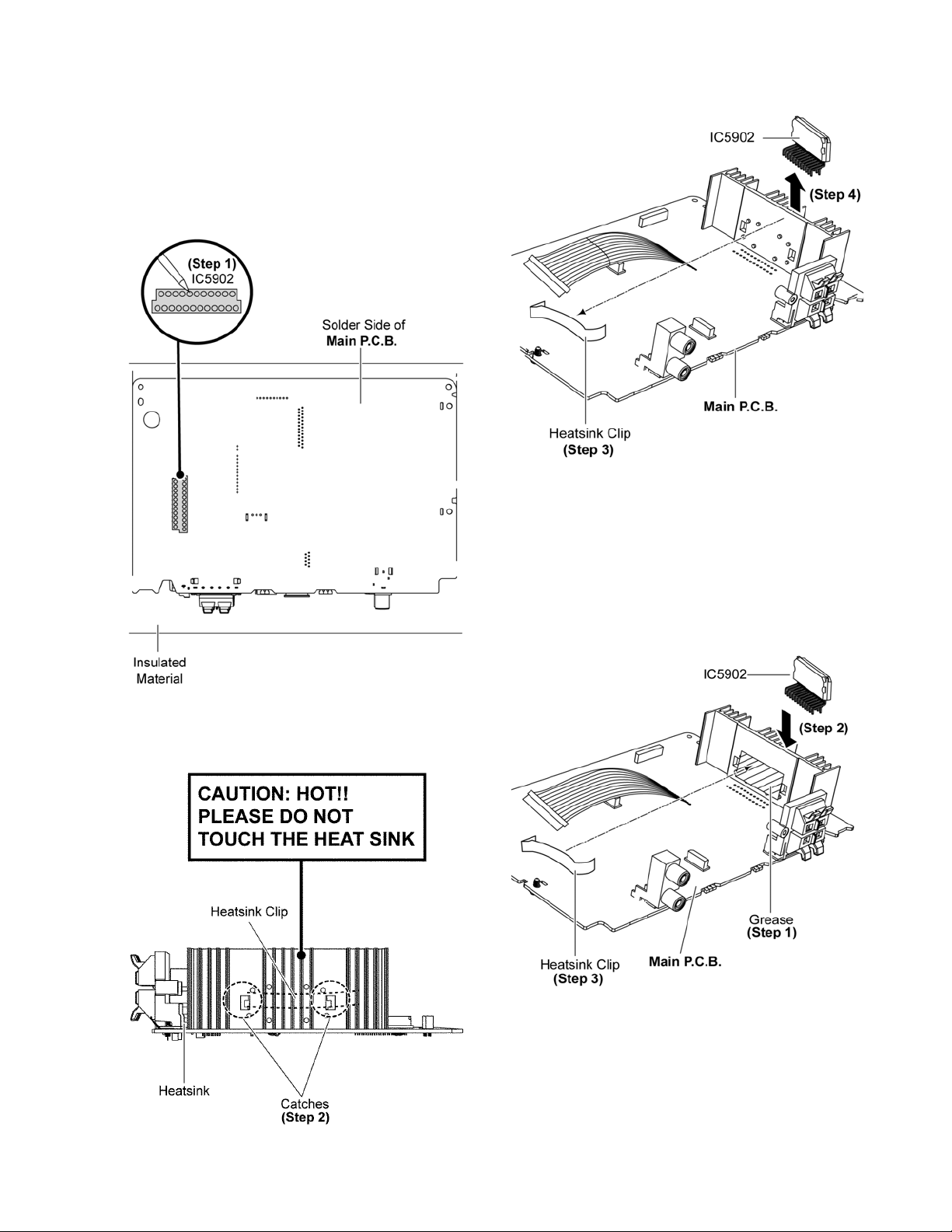
11.13. Replacement of Audio Digital
Amp IC (IC5902)
• Refer to “Disassembly of Main P.C.B.”.
11.13.1. Disassembly of Audio Digital Amp
IC (IC5902)
Step 1 Desolder pins of the Audio Digital Amp IC (IC5902) on
the solder side of Main P.C.B..
Step 3 Remove Heatsink Clip.
Step 4 Remove Audio Digital Amp IC (IC5902).
11.13.2. Assembly of Audio Digital Amp IC
(IC5902)
Step 1 Apply grease to the Heatsink.
Step 2 Fix the Audio Digital Amp IC (IC5902) on Main P.C.B.
Caution: Ensure pins of the Audio Digital Amp IC (IC5902)
are properly seated on Main P.C.B.
Step 3 Fix Heatsink Clip to the Heatsink.
Caution: During assembling, ensure that Heatsink Clip is
catched onto Heatsink properly.
Step 2 Release 2 catches of Heatsink Clip.
Caution: During releasing of 2 catches, avoid touching the
Heatsink, due to high temperature.
44
Page 45
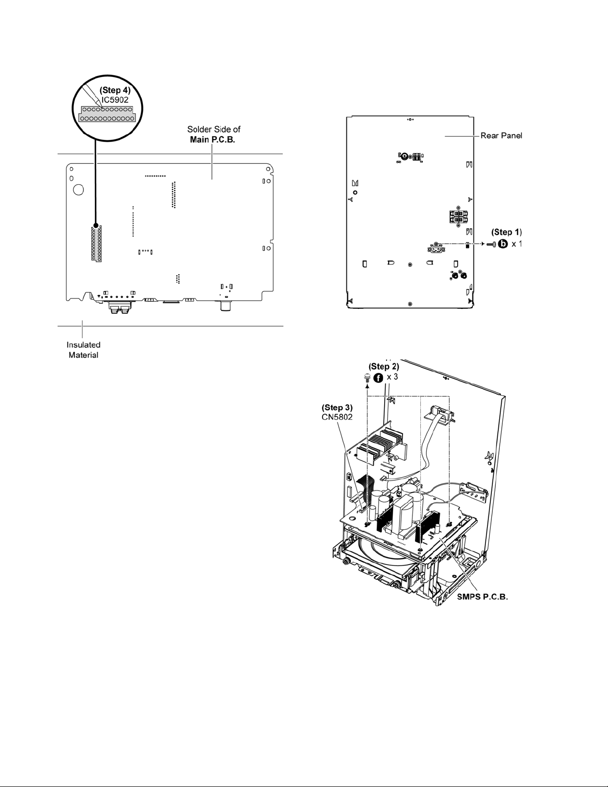
Step 4 Solder pins of the Audio Digital Amp IC (IC5902) on the
solder side of Main P.C.B..
11.14. Disassembly of SMPS P.C.B.
• Refer to “Disassembly of Top Cabinet.”.
• Refer to “Disassembly of Front Panel Unit”.
Step 1 Remove 1 screw.
Step 2 Remove 3 screws.
Step 3 Detach 15P Cable Wire at the connector (CN5802) on
SMPS P.C.B..
45
Page 46
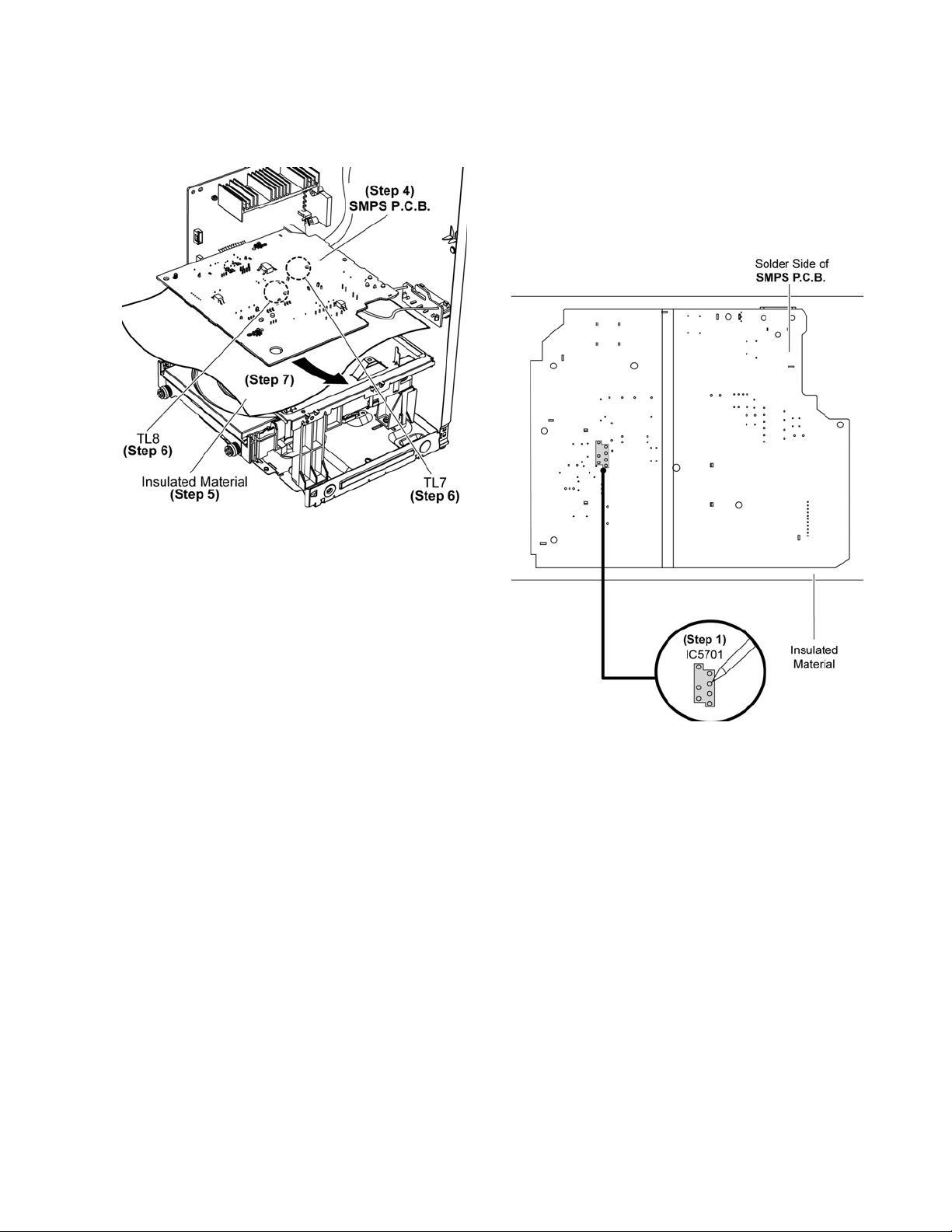
Step 4 Flip the SMPS P.C.B. and position it according to diagram shown.
Step 5 Place SMPS P.C.B. on an insulated material.
Step 6 Desolder 2 Wire pins, TL7 (Black), TL8 (Red).
Step 7 Remove SMPS P.C.B..
11.15. Replacement of Switching Reg-
ulator IC (IC5701)
• Refer to “Disassembly of SMPS P.C.B.”.
11.15.1. Disassembly of Switching Regulator IC (IC5701)
Step 1 Desolder pins of the Switching Regulator IC (IC5701) on
the solder side of SMPS P.C.B..
46
Page 47
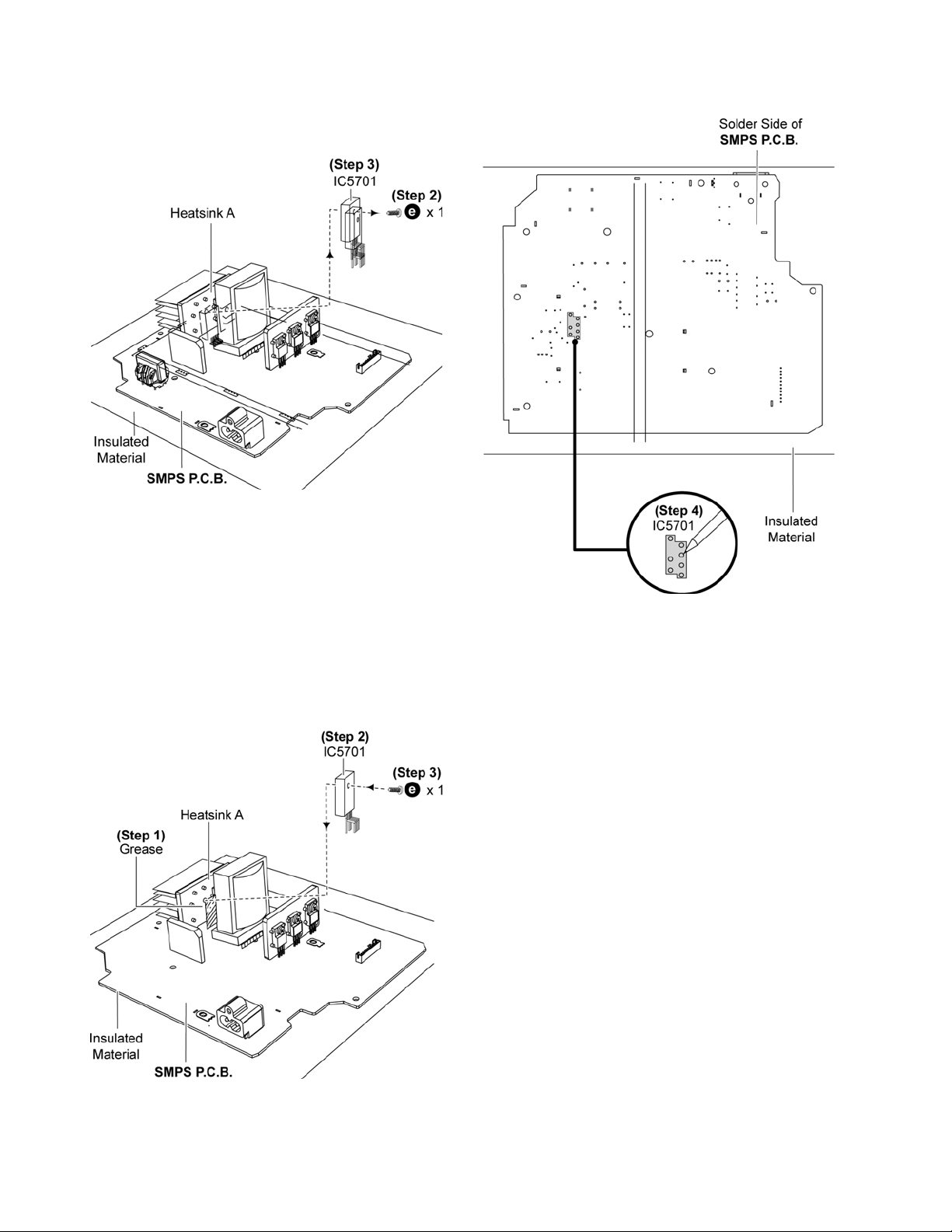
Step 2 Remove 1 screw.
Step 3 Remove the Switching Regulator IC (IC5701).
Caution: Avoid touching the Heatsink A due to its high
temperature after prolonged use. Touching it may lead to
injuries.
11.15.2. Assembly of Switching Regulator
IC (IC5701)
Step 1 Apply grease to the Heatsink A.
Step 2 Fix the Switching Regulator IC (IC5701) to the SMPS
P.C.B..
Caution: Ensure pins of the Switching Regulator IC
(IC5701) are properly inserted and soldered on SMPS
P.C.B..
Step 3 Screw the Switching Regulator IC (IC5701) to the Heat-
sink A.
Caution: Ensure the Switching Regulator IC (IC5701) is
tightly screwed to the Heatsink A.
Step 4 Solder pins of the Switching Regulator IC (IC5701) on
the solder side of SMPS P.C.B..
47
Page 48
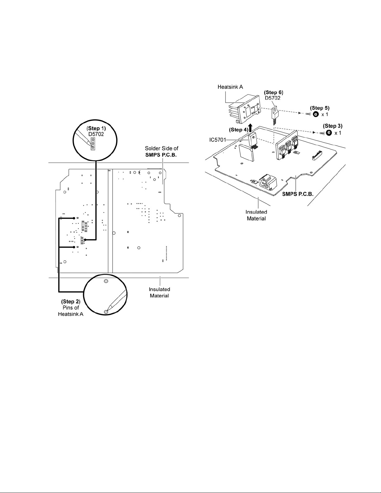
11.16. Replacement of Rectifier Diode
(D5702)
• Refer to “Disassembly of SMPS P.C.B.”.
11.16.1. Disassembly of Rectifier Diode
(D5702)
Step 1 Desolder pins of the Rectifier Diode (D5702) on the sol-
der side of SMPS P.C.B.
Step 2 Desolder pins of the Heatsink A.
Step 3 Remove 1 screw at Switching Regulator IC (IC5701).
Step 4 Remove the Heatsink A with Rectifier Diode (D5702).
Step 5 Remove 1 screw.
Step 6 Remove the Rectifier Diode (D5702) from the Heatsink
A.
Caution: Avoid touching the Heatsink A due to its high
temperature after prolong use. Touching it may lead to
injuries.
48
Page 49
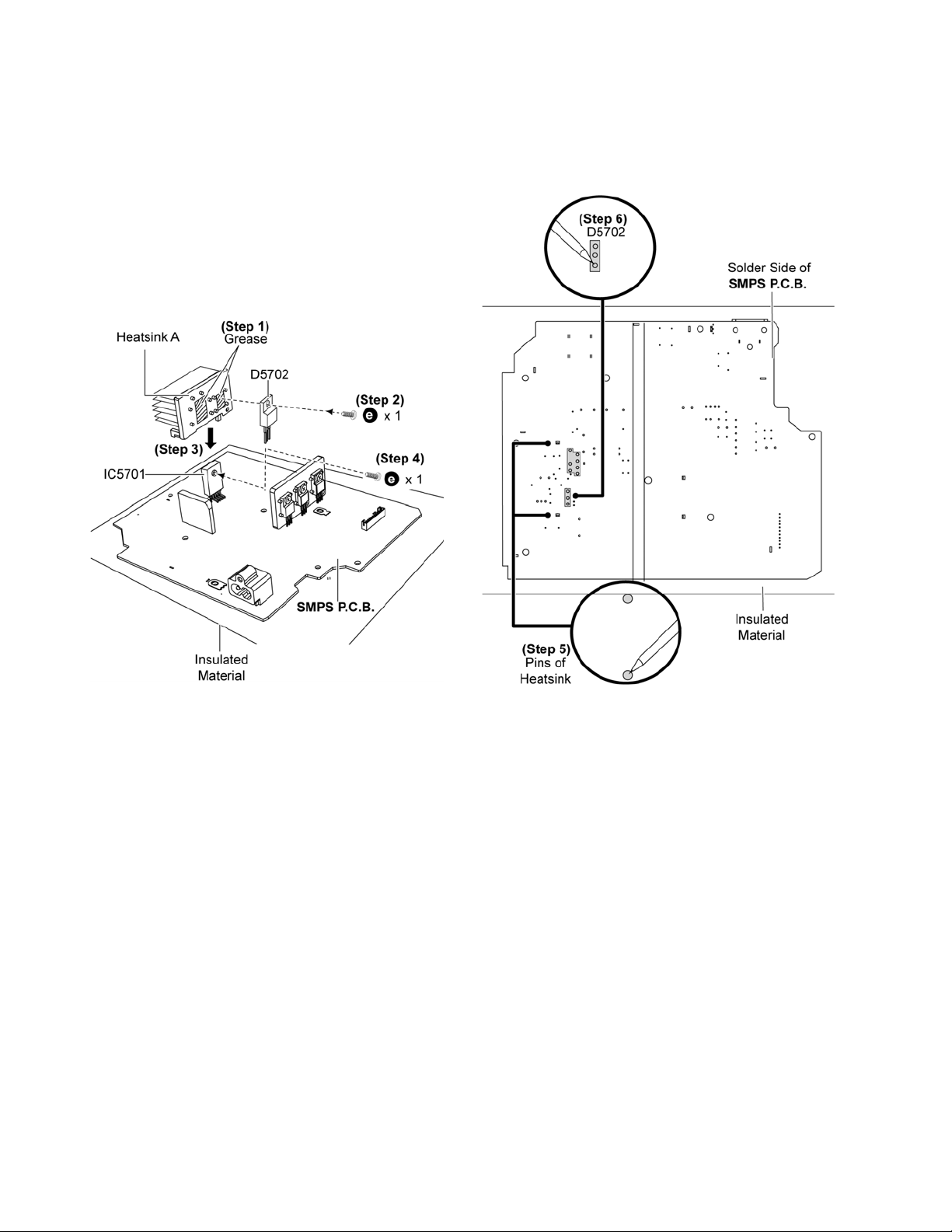
11.16.2. Assembly of Rectifier Diode
(D5702)
Step 1 Apply grease to the Heatsink A.
Step 2 Screw the Rectifier Diode (D5702) to the Heatsink A.
Caution: Ensure the Rectifier Diode (D5702) is tightly
screwed to the Heatsink A.
Step 3 Fix the Heatsink A with Rectifier Diode (D5702) on
SMPS P.C.B. in the direction of arrow.
Caution: Ensure the Heatsink A with Rectifier Diode
(D5702) are properly seated on SMPS P. C.B.
Step 4 Screw the Switching Regulator IC (IC5701) to the Heat-
sink A.
Caution: Ensure that Switching Regulator IC (IC5701) is
tightly screwed to the Heatsink A.
Step 5 Solder pins of the Rectifier Diode (D5702) on the solder
side of SMPS P.C.B..
Step 6 Solder pins of the Heatsink A on the solder side of
SMPS P.C.B..
Caution: Ensure pins of the Rectifier Diode (D5702) are
properly seated and soldered on SMPS P.C.B..
49
Page 50
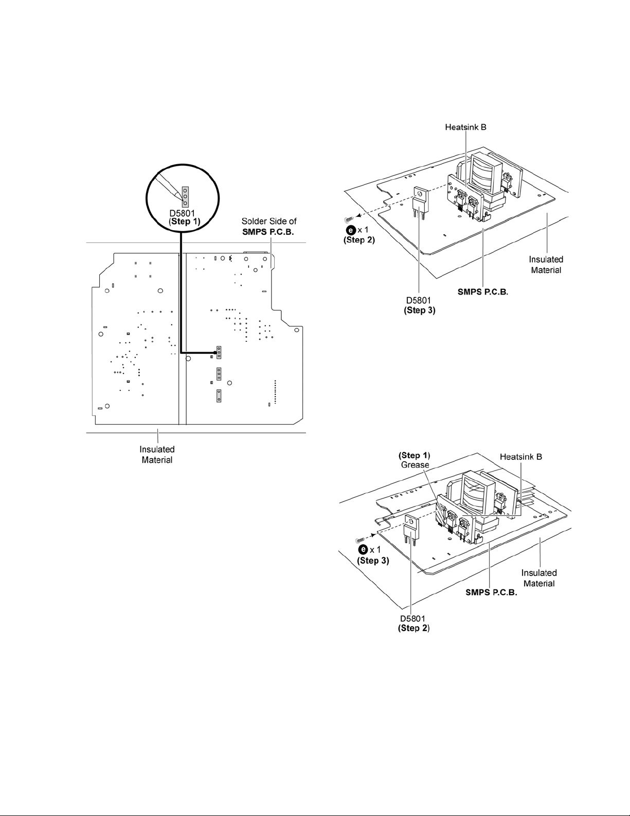
11.17. Replacement of Rectifier Diode
(D5801)
• Refer to “Disassembly of SMPS P.C.B.”.
11.17.1. Disassembly of Rectifier Diode
(D5801)
Step 1 Desolder pins of the Rectifier Diode (D5801) on the sol-
der side of SMPS P.C.B.
Step 2 Remove 1 screw at Rectifier Diode (D5801).
Step 3 Remove the Rectifier Diode (D5801) from the SMPS
P. C . B . .
Caution: Avoid touching the Heatsink B due to its high
temperature after prolonged use. Touching it may lead to
injuries.
11.17.2. Assembly of Rectifier Diode
(D5801)
Step 1 Apply grease to the Heatsink B.
Step 2 Fix the Rectifier Diode (D5801) on SMPS P.C.B.
Caution: Ensure pins of the Rectifier Diode (D5801) is
properly inserted on SMPS P.C.B.
Step 3 Screw the Rectifier Diode (D5801) to the Heatsink B.
Caution: Ensure the Rectifier Diode (D5801) is tightly
screwed to the Heatsink B.
50
Page 51
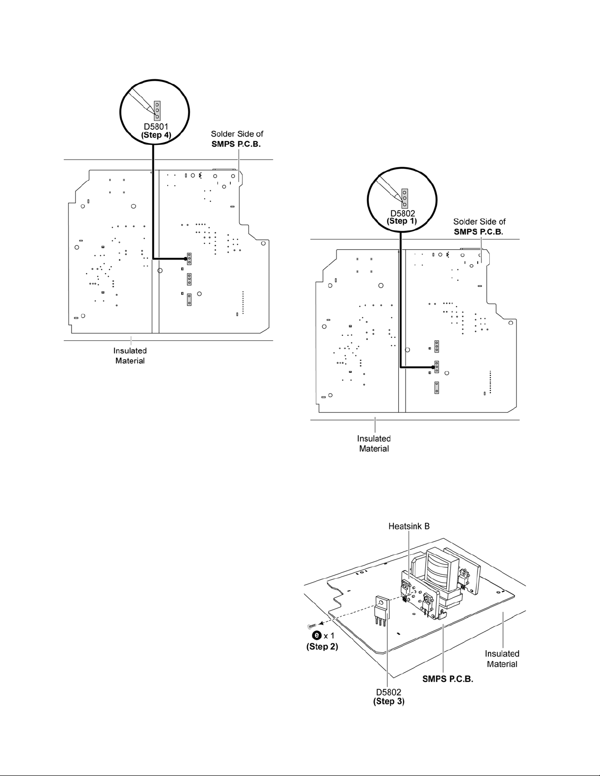
Step 4 Solder pins of the Rectifier Diode (D5801) on the solder
side of SMPS P.C.B..
11.18. Replacement of Rectifier Diode
(D5802)
• Refer to “Disassembly of SMPS P.C.B.”.
11.18.1. Disassembly of Rectifier Diode
(D5802)
Step 1 Desolder pins of the Rectifier Diode (D5802) on the sol-
der side of SMPS P.C.B.
Step 2 Remove 1 screw at Rectifier Diode (D5802).
Step 3 Remove the Rectifier Diode (D5802) from SMPS P.C.B..
Caution: Avoid touching the Heatsink B due to its high
temperature after prolong use. Touching it may lead to
injuries.
51
Page 52
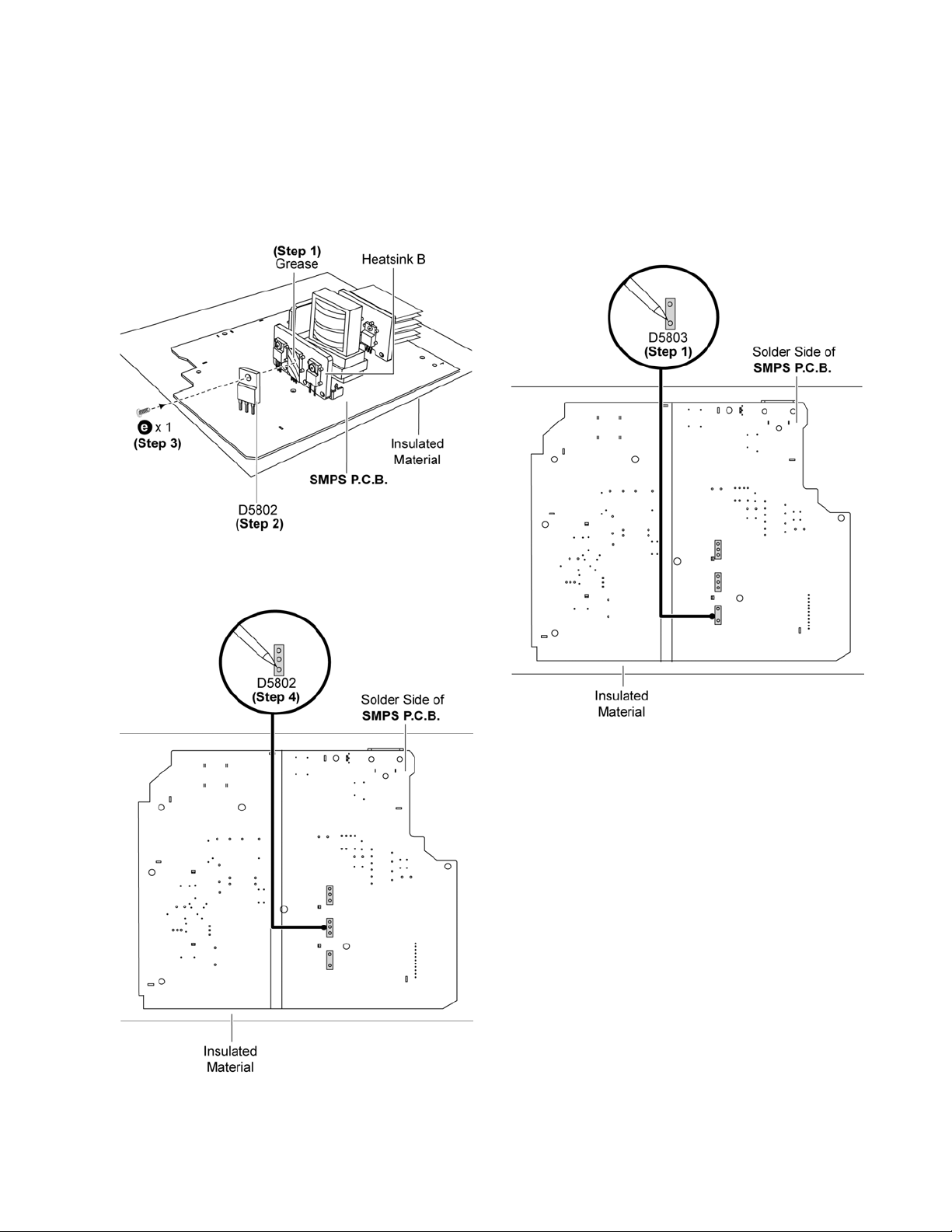
11.18.2. Assembly of Rectifier Diode
(D5802)
Step 1 Apply grease to the Heatsink B.
Step 2 Fix the Rectifier Diode (D5802) on SMPS P.C.B..
Caution: Ensure pins of the Rectifier Diode (D5802) is
properly inserted on SMPS P.C.B.
Step 3 Screw the Rectifier Diode (D5802) to the Heatsink B.
Caution: Ensure the Rectifier Diode (D5802) is tightly
screwed to the Heatsink B.
11.19. Replacement of Regulator
Diode (D5803)
• Refer to “Disassembly of SMPS P.C.B.”.
11.19.1. Disassembly of Rectifier Diode
(D5803)
Step 1 Desolder pins of the Rectifier Diode (D5803) on the sol-
der side of SMPS P.C.B.
Step 4 Solder pins of the Rectifier Diode (D5802) on the solder
side of SMPS P.C.B..
52
Page 53
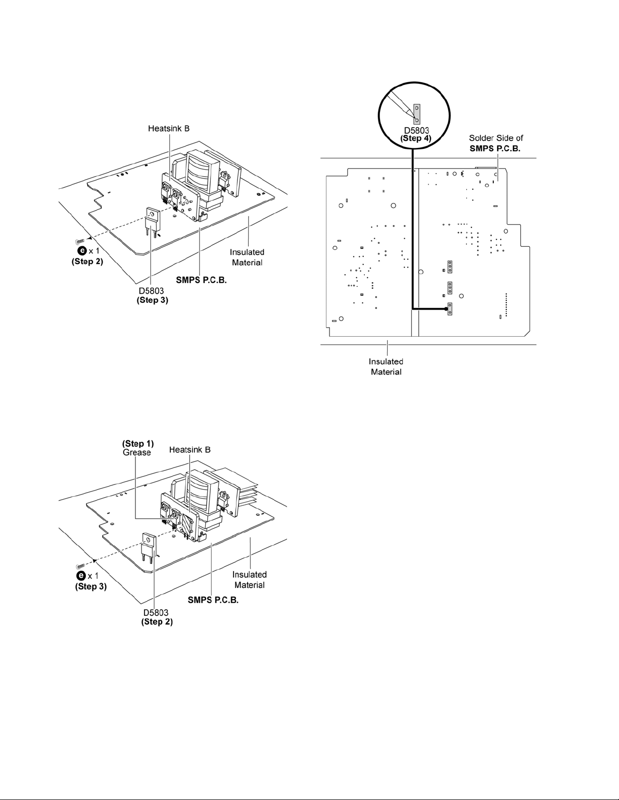
Step 2 Remove 1 screw at Rectifier Diode (D5803).
Step 3 Remove the Rectifier Diode (D5803) from the SMPS
P.C.B..
Caution: Avoid touching the Heatsink B due to its high
temperature after prolonged use. Touching it may lead to
injuries.
11.19.2. Assembly of Rectifier Diode
(D5803)
Step 1 Apply grease to the Heatsink B.
Step 2 Fix Rectifier Diode (D5803) on SMPS P.C.B.
Caution: Ensure pins of the Rectifier Diode (D5803) are
properly inserted on SMPS P.C.B.
Step 3 Screw the Rectifier diode (D5803) to the Heatsink B.
Caution: Ensure the Rectifier Diode (D5803) is tightly
screwed to the Heatsink B.
Step 4 Solder pins of the Rectifier Diode (D5803) on the solder
side of SMPS P.C.B.
53
Page 54
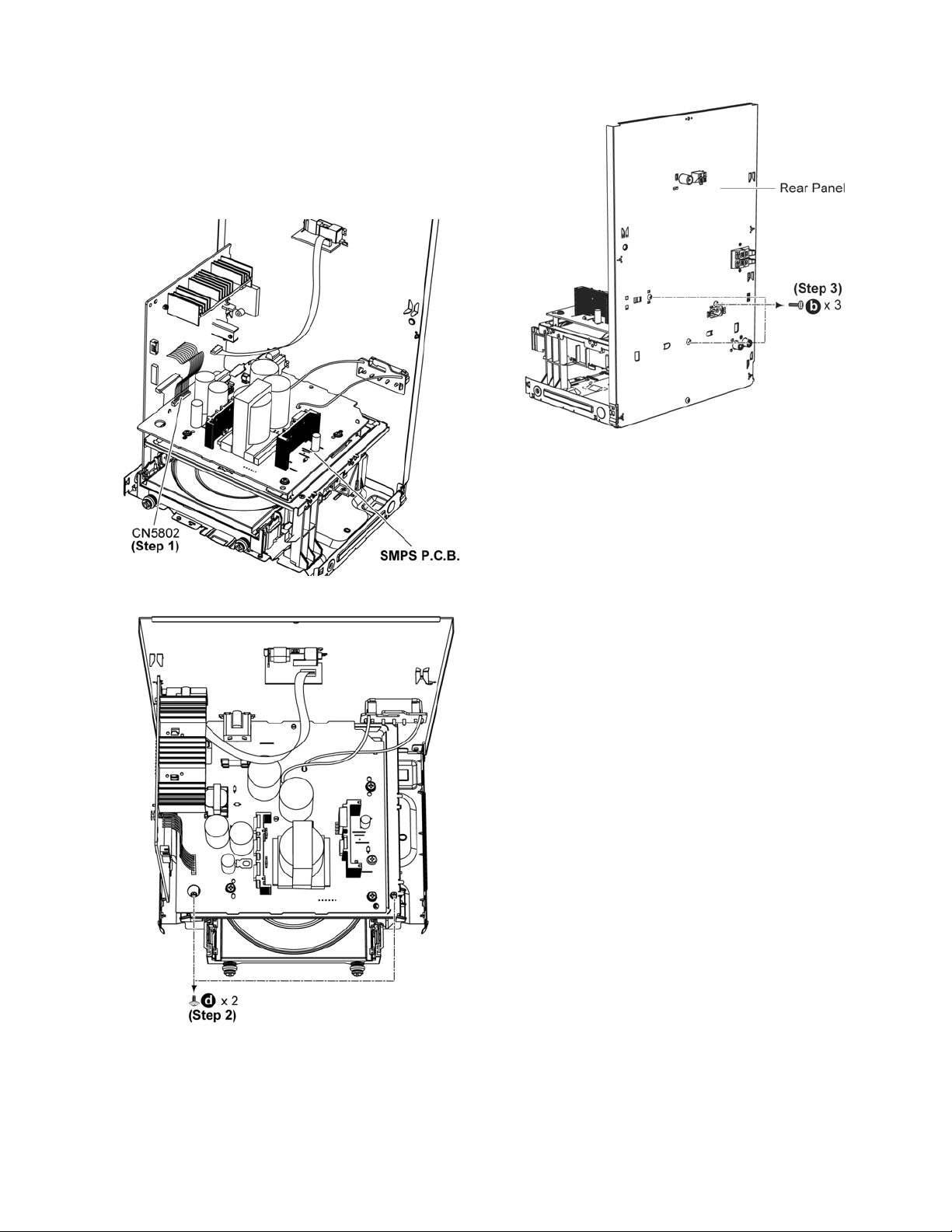
11.20. Disassembly of CD Mechanism Unit (BRS1C)
• Refer to “Disassembly of Top Cabinet”.
• Refer to “Disassembly of Front Panel Unit”.
Step 1 Detach 15P Cable Wire at the connector (CN5802) on
SMPS P.C.B..
Step 3 Remove 3 screws.
Step 4 Detach Voltage Selector P.C.B. from Rear Panel as
arrow shown.
Step 2 Remove 2 screws.
54
Page 55
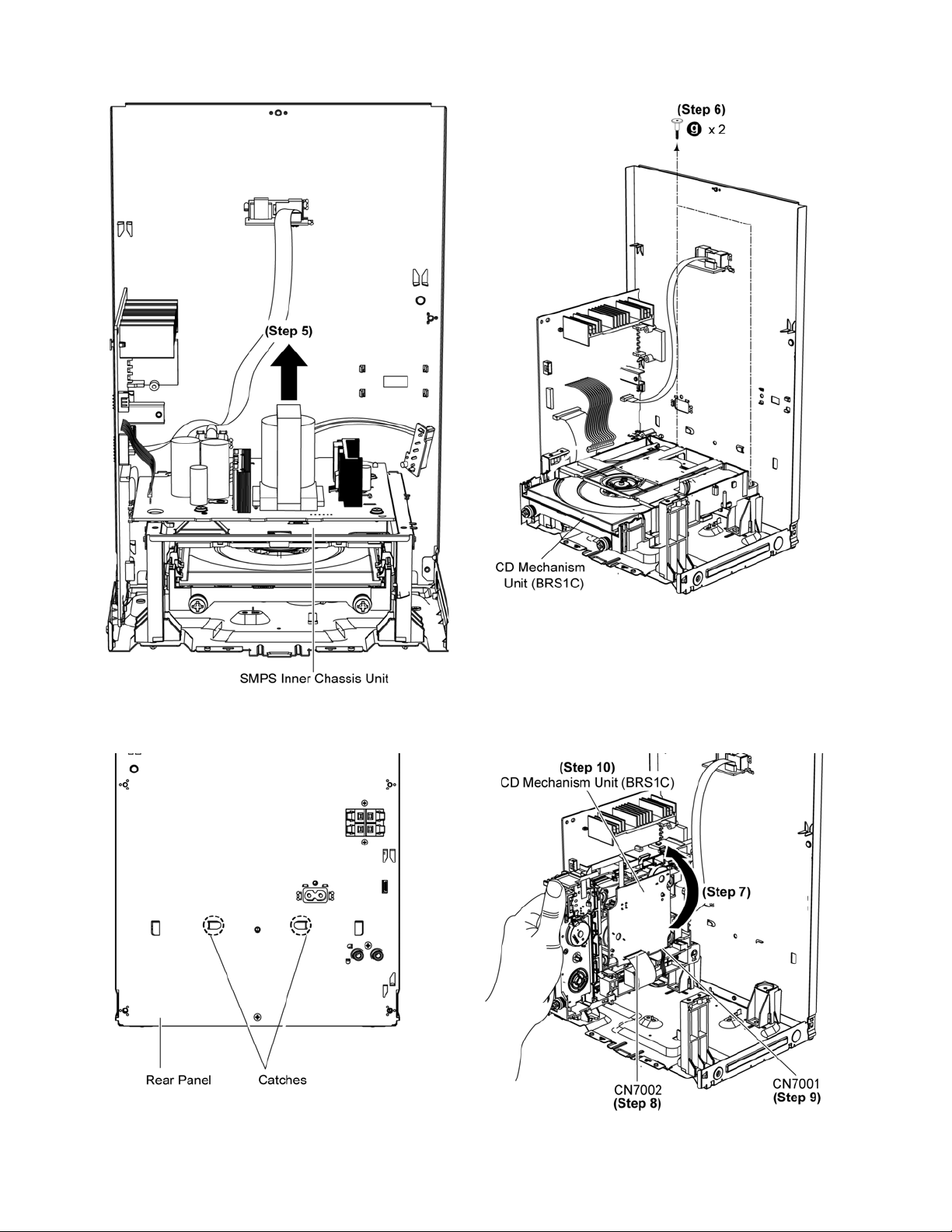
Step 5 Lift up and remove SMPS Inner Chassis Unit.
Step 6 Remove 2 screws.
Caution: During assembling, ensure that SMPS Inner
Chassis is catched onto Rear Panel properly.
Step 7 Lift up & upset the CD Mechanism Unit (BRS1C) as
shown.
Step 8 Detach 27P FFC at the connector (CN7002) on CD
Servo P.C.B..
Step 9 Detach 5P Wire at the connector (CN7001) on CD
Servo P.C.B..
Step 10 Remove CD Mechanism Unit (BRS1C).
55
Page 56
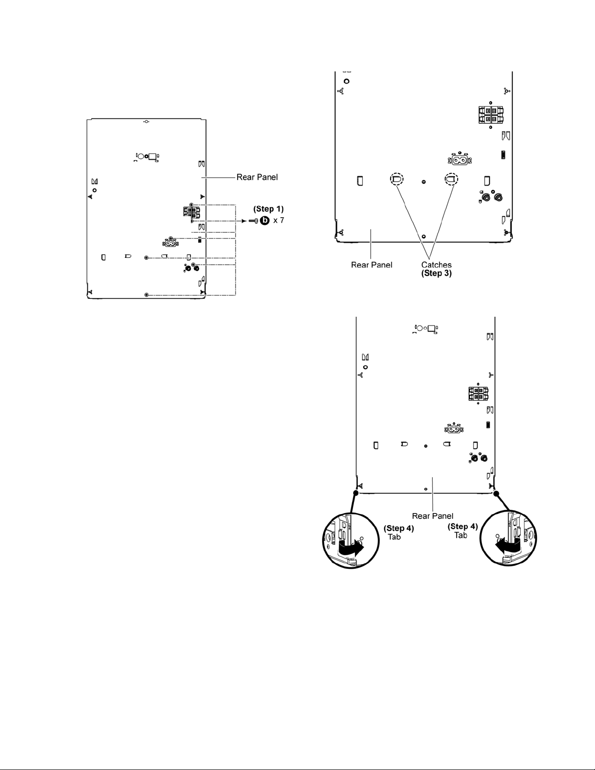
11.21. Disassembly of Rear Panel
• Refer to “Disassembly of Top Cabinet”.
• Refer to “Disassembly of Tuner P.C.B.”.
Step 1 Remove 6 screws.
.
Step 4 Release 2 tabs.
Step 5 Remove Rear Panel.
56
Page 57
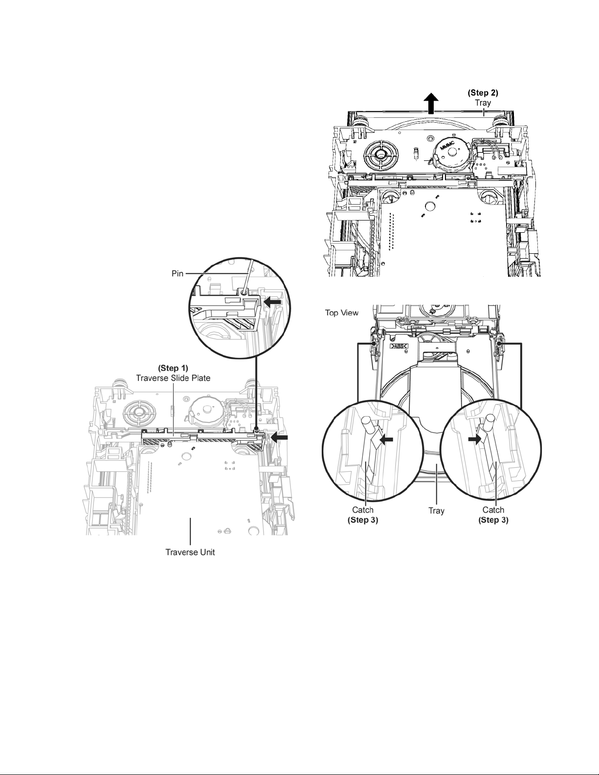
12 Replacement of Traverse Unit
12.1. Disassembly of Traverse Unit
• Refer to “Disassembly of CD Mechanism Unit (BRS1C)”.
Caution: Refer to “2.4 Handling Precaution for Traverse
Unit” to prevent static damage to the Optical Pickup Unit.
Note:
1. When the optical pickup unit is defective, the overall
traverse unit needs replacement.
2. Please note that appropriate actions need to be taken to
prevent static damage.
3. Ensure that the circuit is open before assembly BRS1 to
the main set.
Step 1: Use a pin to slide the Traverse Slide Plate until it come
to a stop.
Step 2: Slide the tray out fully.
Step 3: Release the catches & remove the tray.
57
Page 58
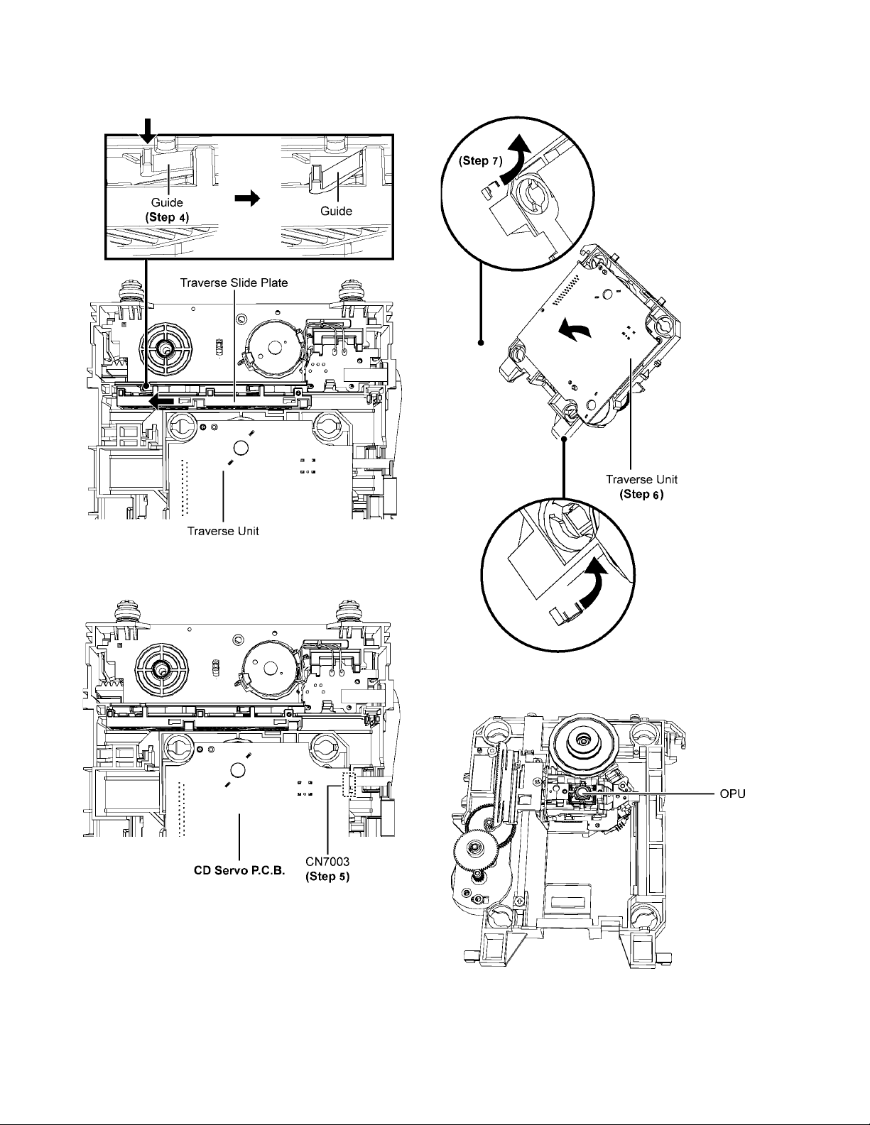
Step 4: Release the guide as shown & slide the Traverse Slide
Plate to the end.
Step 6: Lift the Traverse Unit by approximately 45q.
Step 7: Slide out the traverse unit as arrow shown.
Step 5: Detach 5P FFC at the connector (CN7003) on CD
Servo P.C.B..
Caution: Avoid touching the surface of the Optical Pickup
Unit.
58
Page 59
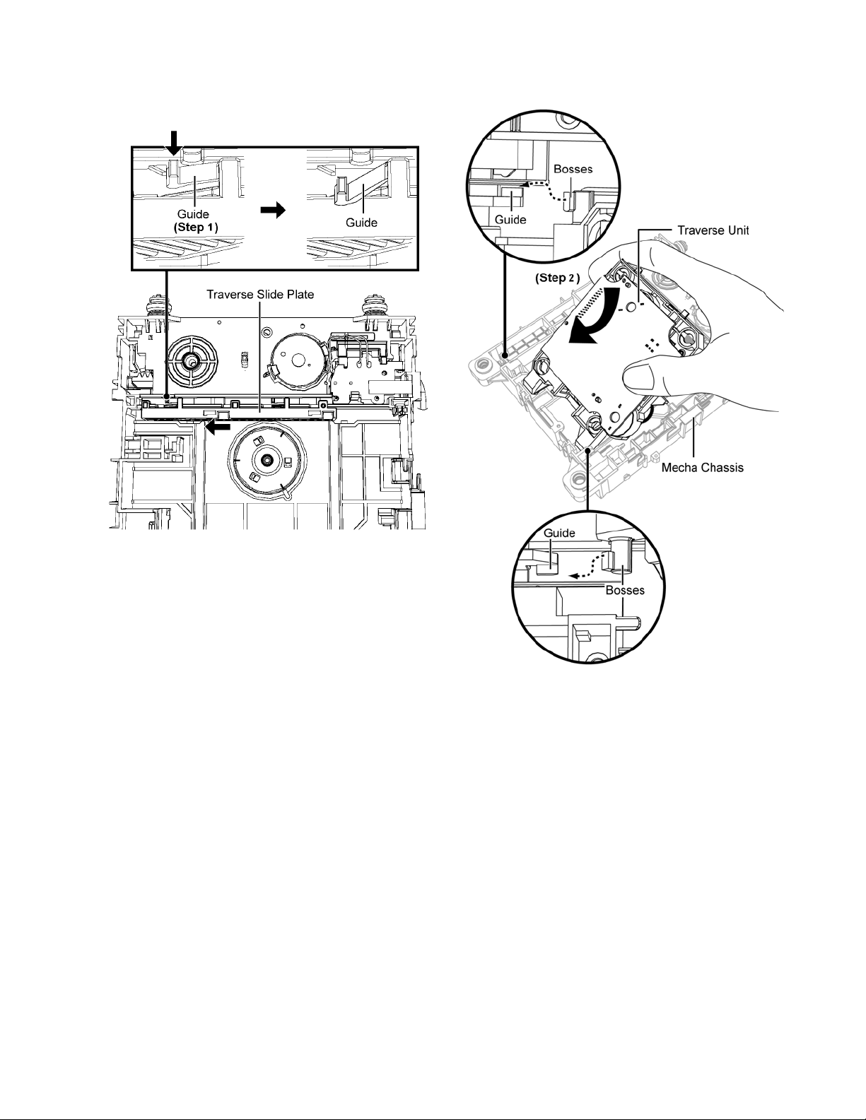
12.2. Assembly of Traverse Unit
Step 1: Release the guide as shown & slide the Traverse Slide
Plate to the end.
Step 2: Slot the Traverse Unit at approximately 45q into the
mecha chassis as arrow shown.
59
Page 60
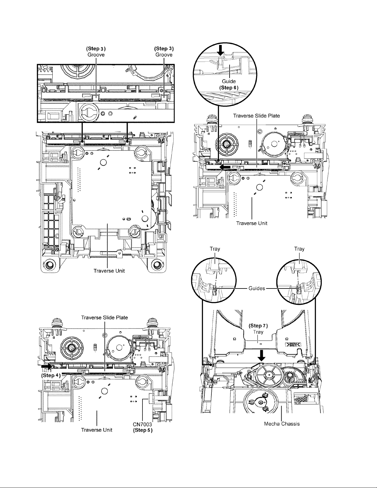
Step 3: Ensure the Traverse Unit seated properly onto the
Groove.
Step 6: Slide the Traverse Slide Plate unit it stop at the Guide.
Step 4: Slide Traverse Slide Plate to lock the Traverse Unit as
shown.
Step 5: Connect 5P FFC at the connector (CN7003) on CD
Servo P.C.B..
Step 7: Slot the Tray into the guides as Picture shown.
60
60
Page 61
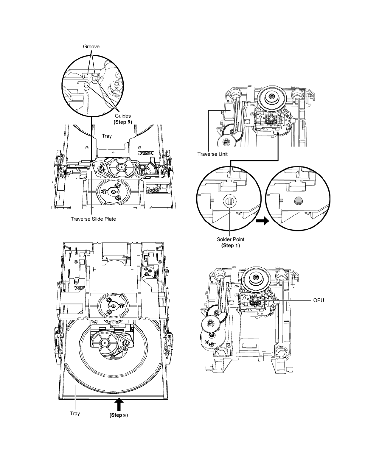
Step 8: Ensure the guides is align with the groove when sliding
the tray in.
12.3. Disassembly of CD Servo
P.C.B.
• Refer to “Disassembly of CD Mechanism Unit (BRS1C)”.
• Refer to “Replacement of Traverse Unit”.
Caution: It is required to short the circuit.
Step 1: Solder the 3 solder points.
Step 9: Slide the tray in fully.
Caution 1: Avoid touching the surface of the Traverse Unit.
61
Page 62
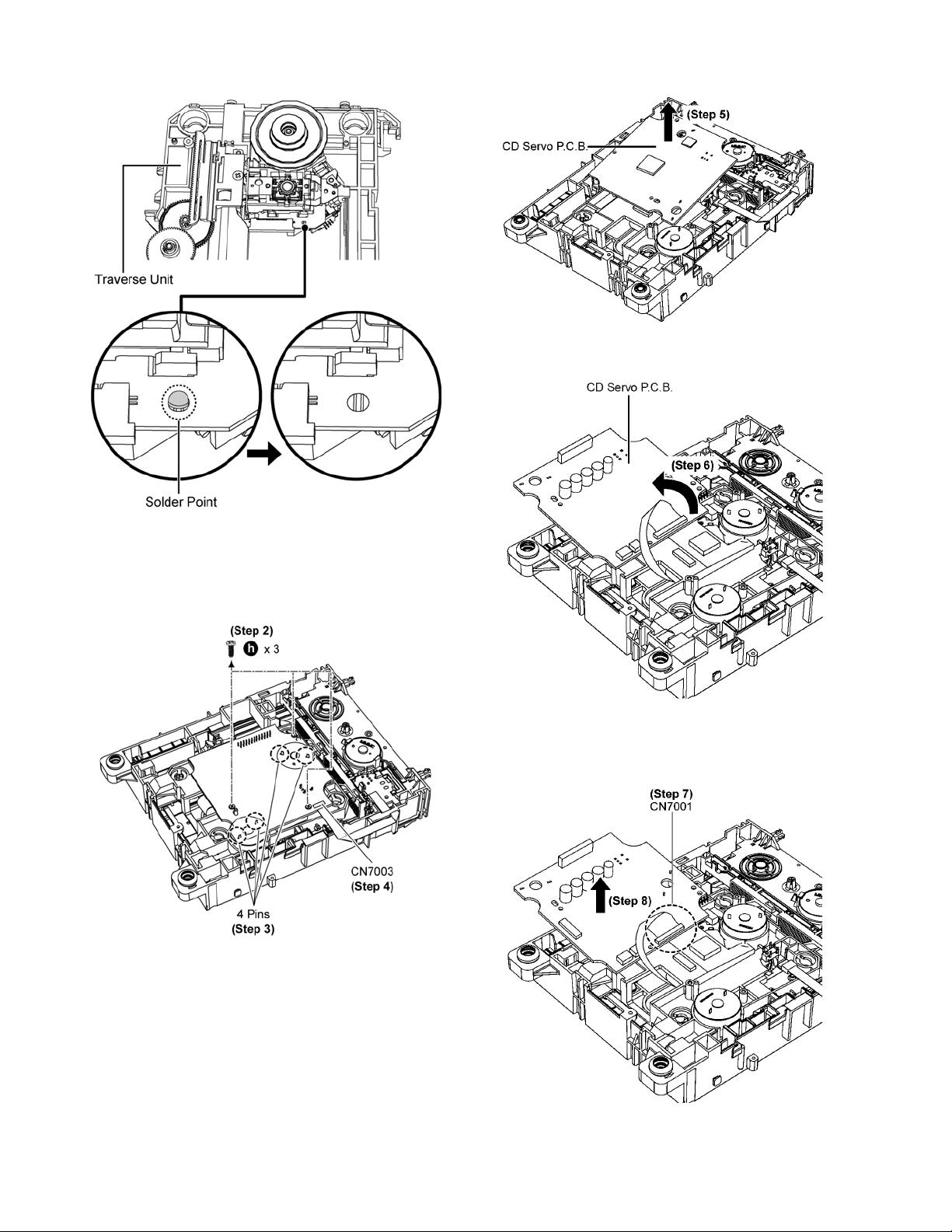
Caution 2: During assembling, desolder the solder points.
Step 5 Slightly lift up the CD Servo P.C.B.
Step 6 Flip the CD Servo P.C.B.
Step 2 Remove 3 screws.
Step 3 Desolder 4 pins.
Step 4 Detach 5P FFC at the connector (CN7003) on CD Servo
P.C.B..
Step 7 Detach 24P FPC at the connector (CN7001) on CD
Servo P.C.B.
Step 8 Remove CD Servo P.C.B..
62
Page 63
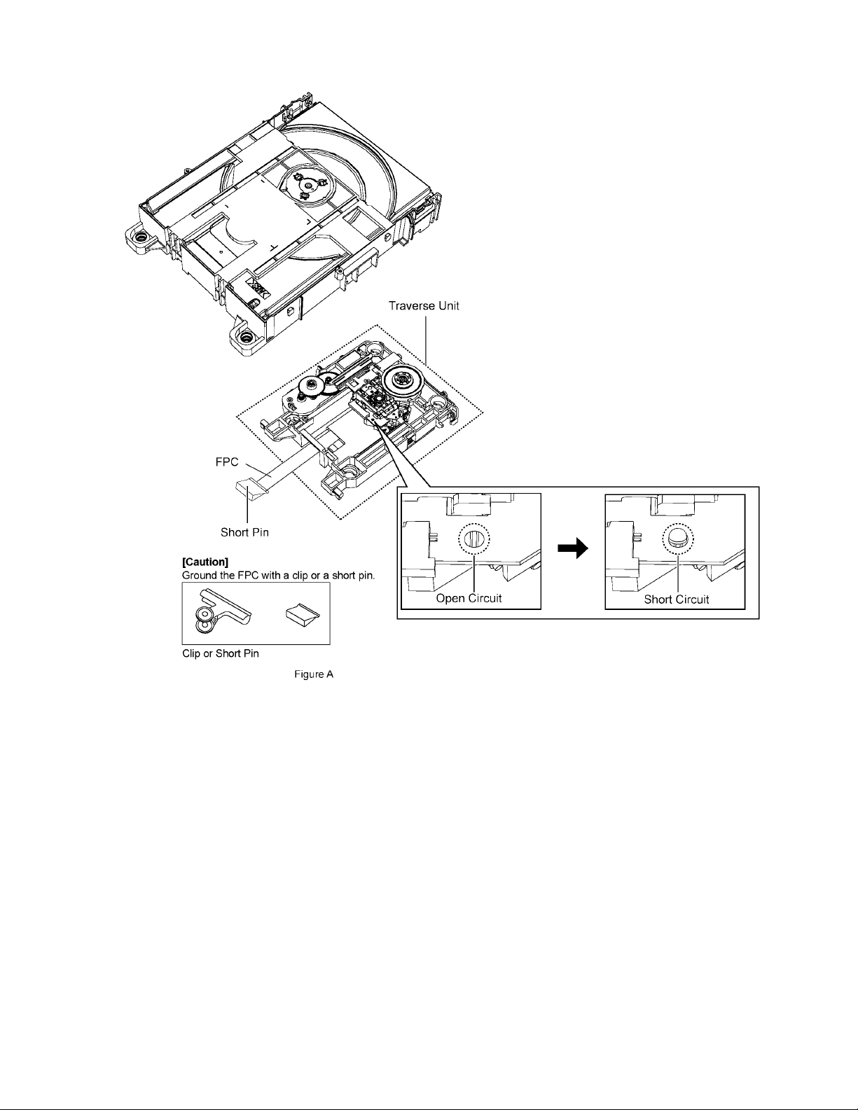
Step 9 Ground the 24P FFC with a short pin.
63
Page 64
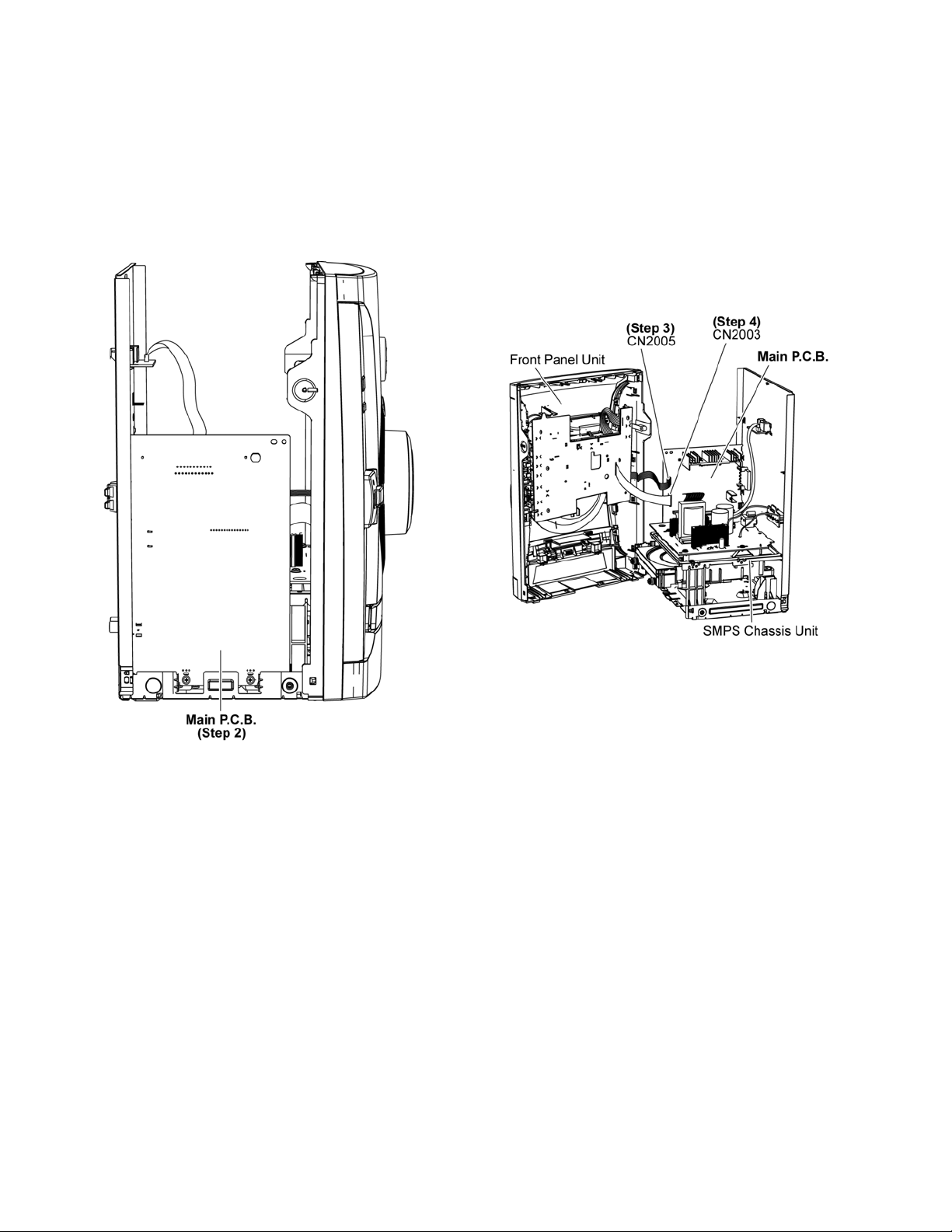
13 Service Position
Note: For description of the disassembly procedures, see
the Section 11.
13.1. Checking and Repairing of
Main P.C.B.
Step 1 Remove Top Cabinet.
Step 2 Main P.C.B. can be checked & repaired at its original
position.
13.2. Checking and Repairing of
Panel P.C.B.
Step 1 Remove Top Cabinet.
Step 2 Remove Front Panel Unit.
Step 3 Attach 5P Cable Wire to the connector (CN2005) on
Main P.C.B..
Step 4 Attach 17P FFC to the connector (CN2003) on Main
P.C.B..
Step 5 Panel P.C.B. can be checked and repaired as diagram
shown.
64
Page 65
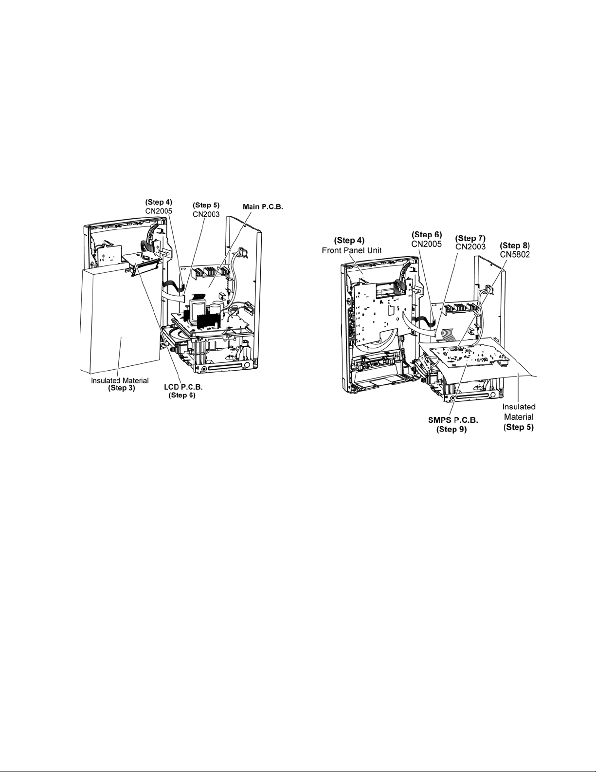
13.3. Checking and Repairing of LCD
P.C.B.
Step 1 Remove Top Cabinet.
Step 2 Remove Front Panel Unit.
Step 3 Position LCD Unit on the insulated material as shown.
Step 4 Attach 5P Cable Wire to the connector (CN2005) on
Main P.C.B..
Step 5 Attach 17P FFC to the connector (CN2003) on Main
P. C .B . .
Step 6 LCD P.C.B. can be checked and repaired as diagram
shown.
13.4. Checking and Repairing of
SMPS P.C.B.
Step 1 Remove Top Cabinet.
Step 2 Remove Front Panel Unit.
Step 3 Remove SMPS P.C.B..
Step 4 Position Front Panel Unit as diagram shown.
Step 5 Position SMPS P.C.B. on the insulated material.
Step 6 Attach 5P Cable Wire to the connector (CN2005) on
Main P.C.B..
Step 7 Attach 17P FFC to the connector (CN2003) on Main
P. C . B . .
Step 8 Attach 15P Cable Wire to the connector (CN5802) on
SMPS P.C.B..
Step 9 SMPS P.C.B. can be checked and repaired as diagram
shown.
65
Page 66
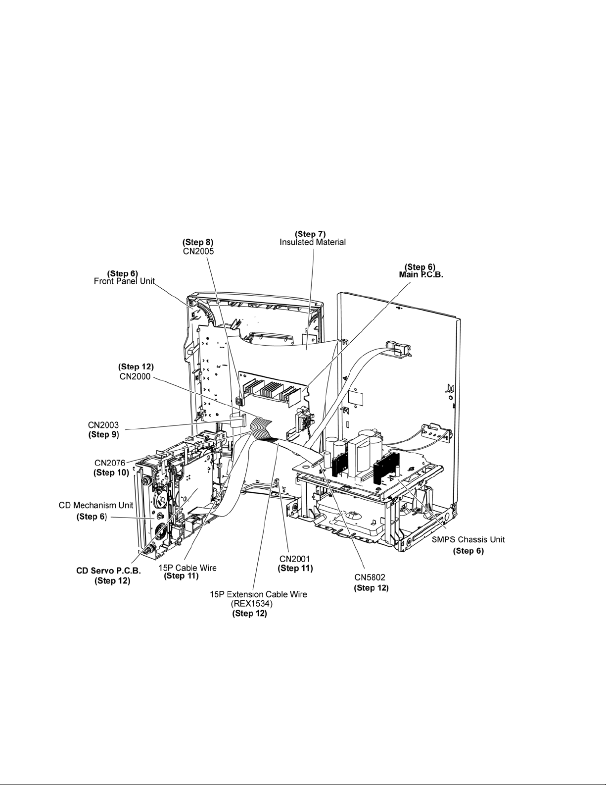
13.5. Checking and Repairing of CD Servo P.C.B.
Step 1 Remove Top Cabinet.
Step 2 Remove Front Panel Unit.
Step 3 Remove SMPS Chassis Unit.
Step 4 Remove CD Mechanism Unit (BRS1C).
Step 5 Remove Main P.C.B..
Step 6 Position Front Panel Unit, SMPS Chassis Unit, CD Mechanism Unit (BRS1C), Main P.C.B as diagram shown.
Step7 Position Main P.C.B. on the insulated material.
Step 8 Attach 5P Cable Wire to the connector (CN2005) on Main P.C.B..
Step9 Attach 17P FFC to the connector (CN2003) on Main P.C.B..
Step 10 Attach 27P FFC to the connector (CN2706) on Main P.C.B..
Step 11 Attach 5P Witre to the connector (CN2001) on Main P.C.B..
Step 12 Extend the Cable Wire with extension Cable Wire (REX1534)(15P Cable Wire) from CN2000 on Main Unit to CN5802 on
SMPS Chassis Unit.
Step 13 CD Servo P.C.B. can be checked and repaired as diagram shown.
66
Page 67
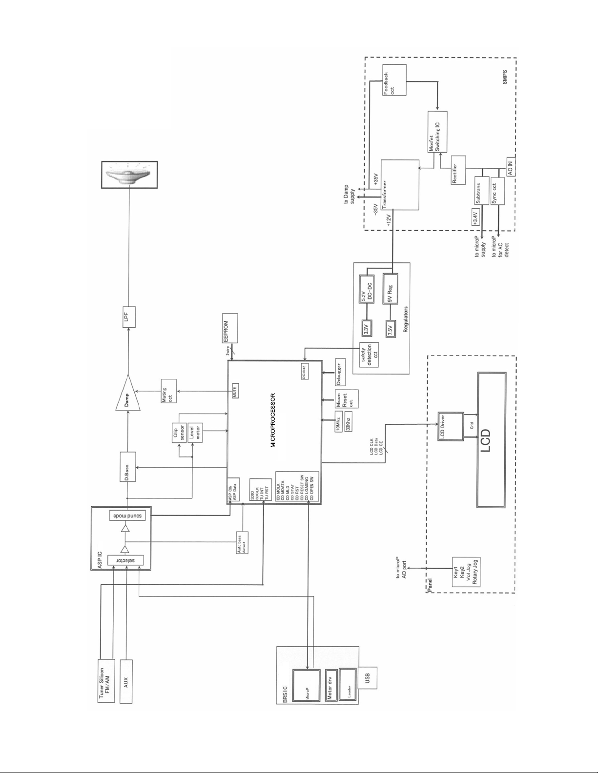
67
14 Simplified Block Diagram
14.1. Overall Simplified Block Diagram
Page 68
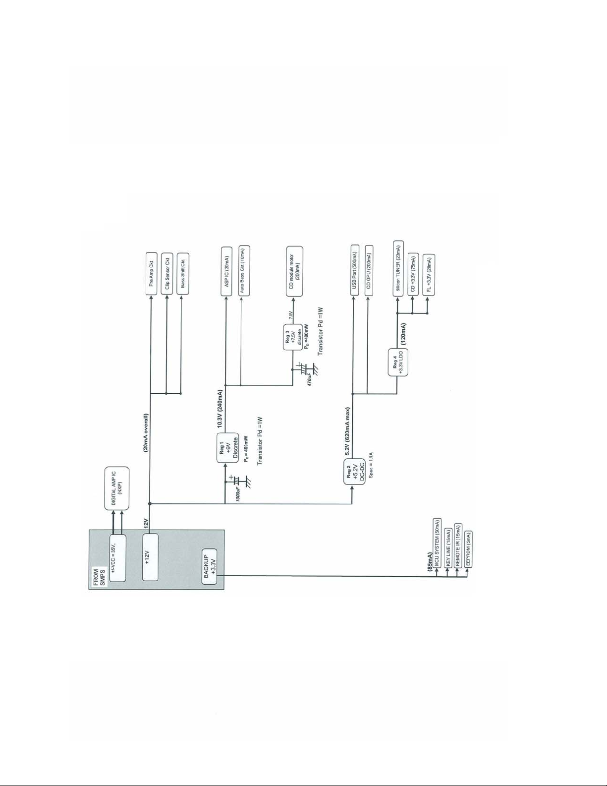
68
14.2. Power Block Diagram
Page 69
USB P.C.B.
USB PORT
JK1111
MAIN P.C.B.
2D-
3D+
D-
D+
33
ZJ6001*CN200522ZJ6001*CN2005
D-
D+
D-
D+
33
CN2001CN790124CN2001CN7901
D-
D+
19USBDM
21USBDP
1 VBUS
VBUS
REMOTE SENSOR P.C.B.
IC2003
MICROPROCESSOR
MN101EF16KXW
in programar, debe ser
3.3V
IR6000
SENSOR
REMOTE CONTROL
3,43,4
CN6006CN6005
117
CN6001CN2003
RMT
RMT 85
IC2006
C3EBEY000037
rogramado.
Z900
LCD
IC900
LCD DRIVER
C0HBA0000295
EE SCL60
6SCL
EEPROM
S6013
STOP
PLAY/PAUSE
RADIO/EXT-IN
CD
USB
ALBUM/TRACK
OSC2(OUT) 12
CD S REQ
721
CN7002 CN2706
CD S REQ
91STATUS CD SO35
820
48MN947 REQUEST OUT CD S REQ29
KEY2
CN6001CN2003
KEY2
CD USB INCD USB IN
CN7002 CN2706
55USBIN CD USB IN46
OPEN/CLOSE
VR6002
ALBUM/TRACK
ROTARY JOG
513
CN6001CN2003
ROTARY JOG
ROTARY JOG 96
NRST19
VR6001
VOL JOG
CN6001CN2003
VOL JOG
VOL JOG 98
VOLUME
135
PANEL P.C.B.
PCONT
PCONT
PCONT 7
SMPS BP
SMPS BP
SMPS BP 74
FROM/TO
POWER SUPPLY
SYNC
DC ENABLE
SYNC
DC ENABLE
DC DET PWR
SYNC 26
DC-DC ENABLE 78
DC DET PWR
DC DET PWR 23
BASS SHIFT
FHOP
BASS SHIFT
BASS SHIFT 24
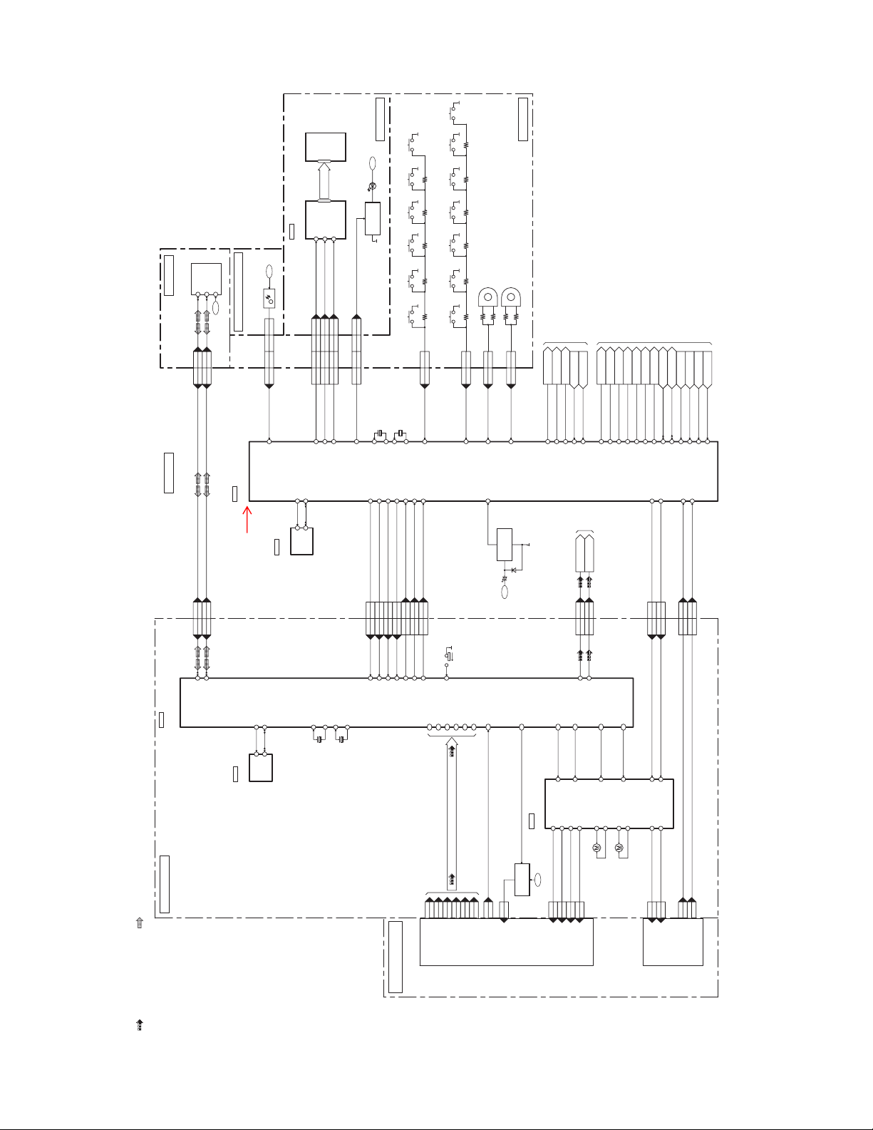
SA-AKX14 SERVO & SYSTEM CONTROL BLOCK DIAGRAM
FROM/TO
AUDIO
FHOP
MUTE F
ASP CLK
MODE DA
MUTE F
ASP CLK
MODE DA
FHOP 73
MUTE F 75
ASP CLK 20
MODE DA 68
TU SCLK
TU SCLK
TU SCLK 81
TU RST
LD CCW66
TU RST
TU RST 80
ASP DATA
ASP DATA
ASP DATA 21
LD CW65
TU SDA
TU SDA
TU SDA 79
TU INT
TU INT
TU INT 87
DC DET AMP
DC DET AMP
DC DET AMP 22
CD CLOSE SW43
CLIP SENSOR
CD OPEN SW48
AUTO BASS
CLIP SENSOR
AUTO BASS
AUTO BASS 95
CLIP SENSOR 94
LATIN
S6012
PRESET EQ
S6005
FORWARD
S6004
REWIND
S6003
MANUAL EQ
D.BASS
S6002
S6001
POWER
KEY1
315
414
CN6001CN2003
KEY1
KEY1 92
KEY2 93
TO AUDIO
RESET
Q2011
D2008
3.3V
12 16
RESET
S7201
66RESTW
CD-L
LOUT
CN7002 CN2706
LOUT
1OUTL
CD-R
CD CLOSE SW
ROUT
17 11
19 9
CN7002 CN2706
ROUT
5OUTR
LD CCW
CN7002 CN2706
LD CCW
CD OPEN SW
LD CW
325
24 4
23 5
27 1
CN7002 CN2706
CN7002 CN2706
CN7002 CN2706
LD CW
CD OPEN SW
CD CLOSE SW
69
LCD P.C.B.
S6011
5V
S6010
SEG0 ~ SEG31
/WR1/CS
3
LCD CE
55
CN6000ZJ6002*
810
CN6001CN2003
LCD CE
LCD CE 32
LCD WR 33
D993
S6009
LED DRIVE
Q900
S6008
S6007
DIMMERDIMMER
66
CN6000ZJ6002*
711
CN6001CN2003
DIMMER 28
S6006
22
153
X2000
X2001
XI 15
XO 16
OSC1(IN) 13
CD SCLK
CD RESET44
36
34
42
CD SO
CD RESET
CD SCLK
CD SI
CD MREQ
622
919
11 17
10 18
CN7002 CN2706
CN7002 CN2706
CN7002 CN2706
CN7002 CN2706
CN7002 CN2706
CD SO
CD SI
CD SCLK
CD MREQ
CD RESET
72NRST
93MCLK
92MDATA CD SI
47MN16K REQUEST IN CD MREQ
COM0 ~ COM3
DATA
4
LCD DATA
LCD WR
44
CN6000ZJ6002*
CN6000ZJ6002*
99
CN6001CN2003
CN6001CN2003
LCD WR
LCD DATA
LCD DATA 31
EE SDA61
5SDA
IC7001
SERVO
PROCESSOR
MN6627947RC
CD SERVO P.C.B.
: USB SIGNAL LINE
: CD AUDIO INPUT SIGNAL LINE
15 Block Diagram
15.1. Servo & System Control
IC7851
EEPROM
C3EBFC000042
SPOUT
FOP
C
126
CN7001
PD
D
E
F
124
122
123
CD TRACKING SIGNAL
20
19
14
10
CN7001
CN7001
CN7001
128
MD/LPD
CN7001
LD
129
LASER DRIVE
Q7601
CD-LD
5
6
CN7001
A
BRS1C
127
16
CN7001
OPTICAL
PICKUP UNIT
B
125
CN7001
15
EECLK73
EEDATA75
6EE CLK
5EE DAT
MX123
MX224
X19
X210
X7205
X7201
118
26VINTK
VOTK+15
VOTK-16
VOFC-13
IC7002
5CH MOTOR DRIVER
C0GBY0000117
LDSW
F+F-T+
T-
23
CN700124CN700122CN700121CN7001
TRP
117
1VINFC
VOFC+
14
VOLD+17
+
M7301*
SPINDLE MOTOR
114
23VINLD
VOLD-18
VOSL+11
+
M7302*
TRAVERSE MOTOR
TRVP
115
7REV
6FWD
4VINSL
VOSL-12
VOTR+10
VOTR-9
SW OPEN
SW CLOSE
LDM+
LDM-
4
5
1
CN7003
CN7003
CN7003
3
CN7003
LOADING P.C.B.
CD MECHANISM UNIT
NOTE: “ * ” REF IS FOR INDICATION ONLY
Page 70
SPEAKERS
15
BOOT2
LEFT
-
+
4
JK50003JK5000
14
OUT2
RIGHT
-
+
1
JK50002JK5000
9
10
OUT1
BOOT1
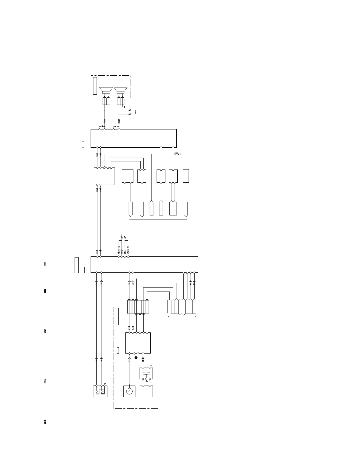
SA-AKX14 AUDIO BLOCK DIAGRAM
: AM SIGNAL LINE : FM SIGNAL LINE
IC5902
C1BA00000497
IC2201
MAIN P.C.B.
IC2101
IN2-
AUDIO DIGITAL
AMPLIFIER
21
FR
FL
DUAL OP-AMP
C0ABBB000067
Q2040,Q2041,Q2220,
Q2222,QR2400,QR2402
LOUT 31
ASP
C1BB00001151
10 INL4
IN1+
2
ROUT 32
PRE-AMP
4 INR4
&
CIRCUIT
BASS SHIFT
CIRCUIT
AUTO BASS
Q2038,Q2039
VOLINL 22
IGOUTL 21
VOLINR 24
IGOUTR 23
TUNER P.C.B.
AUTO BASS
AUTO BASS
12 INL2
L OUT
82
CN2010CN5164CN2010CN51
L OUT
R OUT
R OUT
2 INR2
Q2050,Q2051
TU SDA
TU SCLK
46
CN2010CN5137CN2010CN51
TU SDA
TU SCLK
CIRCUIT
CLIP SENSOR
CLIP SENSOR
CLIP SENSOR
TU INTTU INT
TU RST
28
CN2010CN51
CN2010CN51
TU RST
Q5900,QR5900,QR5901
BASS SHIFT
BASS SHIFT
FROM/TO
19
OSC
MODE
1
23
TH5900
MODE
CIRCUIT
CIRCUIT
HOPPING
CONTROL
SELECTION
FREQUENCY
Q5901,Q5902,Q5903
FHOP
MOD DA
MUTE F
FHOP
MUTE F
MODE DA
SERVO & SYSTEM CONTROL
TU SCLK
TU RST
TU INT
TU INT
TU RST
TU SCLK
TU SDA
TU SDA
SWITCH
SPEAKER
Q5904,Q5905
PROTECTION
DC DET AMP
DC DET AMP
18 SCL
19 SDA
ASP DATA
ASP CLK
ASP CLK
ASP DATA
70
8 DIFFL
6 DIFFR
CD-L
CD-R
CD-L
CD-R
: AUX/TUNER AUDIO INPUT SIGNAL LINE : AUDIO OUTPUT SIGNAL LINE: CD AUDIO INPUT SIGNAL LINE
15.2. Audio
JK2000
RST 5
SDIO 8
SCLK 7
LOUT 14
ROUT 13
IC52
AM/FM
RADIO RECEIVER
REP4780A
GCGPIO2 18
2 FMI
4 AMI
9 RCLK
17 DCLK
FROM/TO
SERVO & SYSTEM CONTROL
X51
4
6
L52
FM ANT
312
2
1
JK52
AM ANT
AUX-L
AUX-R
312
L
R
JK51
AUX IN
Page 71
1
SYS3.3V,DVREF+
BLOCK (2/2)
TO POWER SUPPLY
FROM/TO
SERVO & SYSTEM CONTROL
3
2
+5V
CD 3.3V
4
CD+7.5V
CN2000CN5802
SYS3.3V SYS3.3V
3.3V
SYS3.3V,DVREF+
SYNC
PCONT
SMPS BP
SMPS BP
DC ENABLE
DC ENABLE
DC DET PWR
5V
+5V
4102D5102D
CD 3.3V
VOUT 5
IC2009
C0DBFYY00049
+3.3V VOLTAGE
REGULATOR
1 VIN
3CE
+5V
+5V
35V
+35V SENSE
-35V
-35V SENSE
Q2021
9V
+9V+9V
REGULATOR
+9V VOLTAGE
DC16V
D2000
+7.5V
D2004
Q2022
VOLTAGE
CONTROL
REGULATOR
+7.5V VOLTAGE
Q2000
DC16V
D2017
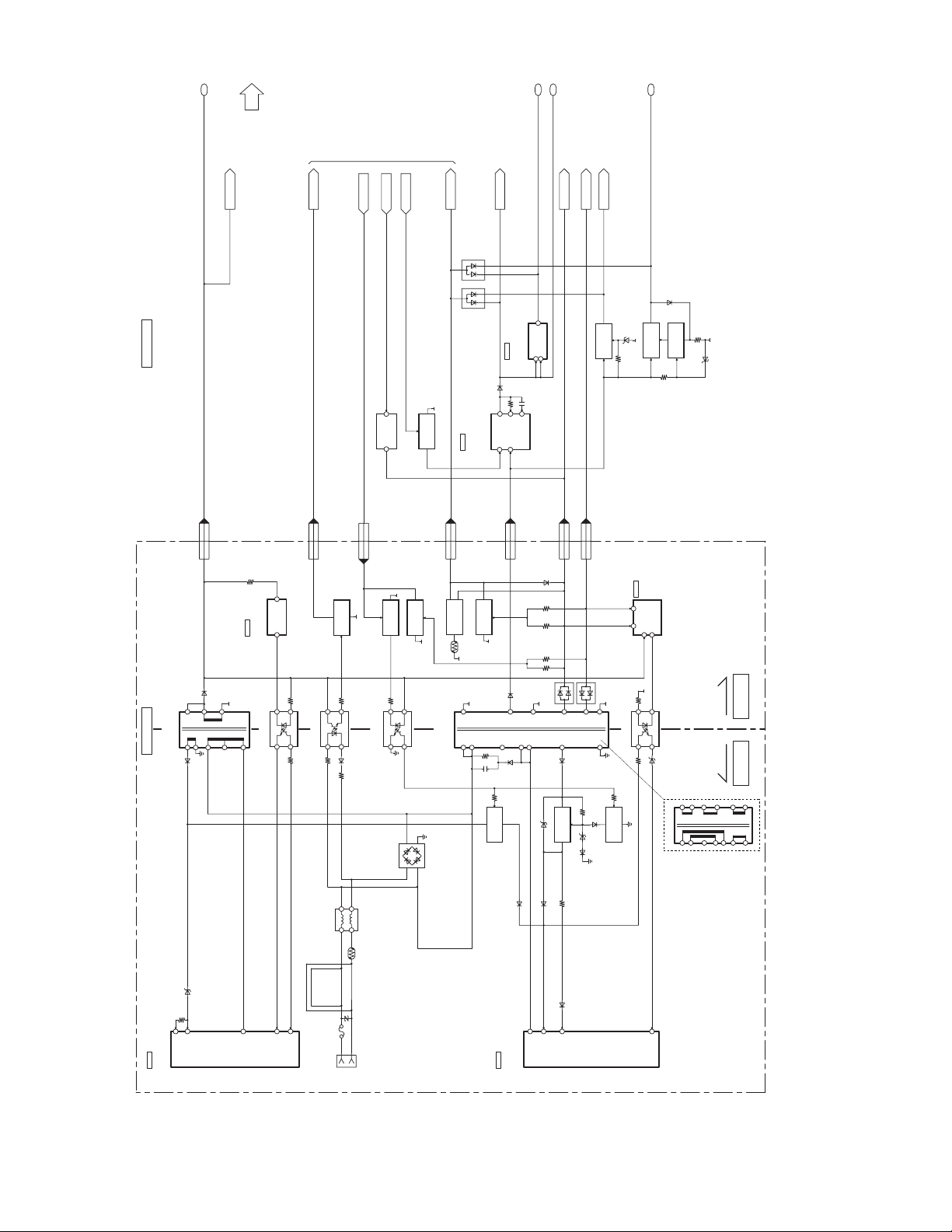
SA-AKX14 POWER SUPPLY (1/2) BLOCK DIAGRAM
D2022
+5V
FB 5
SW 3
AM
Q2035
SYNC SYNC
88
IC5899
SHUNT
REGULATOR
C0DAEYY00040
CN2000
CN5802
SYNC
KC RR
PCONT PCONT
77
CN2000
1414
CN5802
PCONT
SWITCH
Q5898
QR5810
CIRCUIT
BEATPROOF
PCONT
SWITCH
QR5801
SWITCH
QR2001
SWITCH
IC2011
C0DBAYY01122
DCDET2 DC DET PWR
1010
CN2000
CN5802
DCDET2
DETECT
TEMPERATURE
TRANSFORMER
Q5860,Q5861,Q5862
+5V VOLTAGE
QR5802
EN
SWITCHING
REGULATOR
7
DC DETECT
2 VIN
DC16V
DC16V
CN2000
CN5802
DC16V
BST 1
-35V SENSE
1313
5,65,6
1,21,2
CN2000CN5802
CN2000CN5802
D5804
-35V SENSE
+35V SENSE +35V SENSE
IC5801
SHUNT
REGULATOR
C0DAZYY00039
CIRCUIT
FEEDBACK
71
TH5860
SUB
TRANSFORMER
T5751
SMPS P.C.B. MAIN P.C.B.
CL 3
IC5799
SWITCHING MODE POWER
SUPPLY CONTROL
MIP2F20MSSCF
15.3. Power Supply
D5798
D5795
8
5
632
VCC 4
D5802
D5896
2
1
4
PC5702
3
SYNC
1
2
7
10
PC5799
FEEDBACK
3
1
4
PC5701
FEEDBACK
2
1
3
4
MAIN
TRANSFORMER
T5701
D5803
14
4
151211
5
786
D5730
D5801
1
PC5720
FEEDBACK
2
4
3
SECONDARYPRIMARY
D5725
9
10
1
2
D5731
D5702
D5721
SWITCH
Q5721
VOLTAGE
REGULATOR
D5701
4
1
L5705
3
2
D5729
D5726
SWITCH
LIMITING
CURRENT
Q5722
D5722
D5723
D5728
Q5720
149151211
5
4
10
12786
TH5702
DZ5701
D5
FB 2
F1
VDD 1
AC INLET
P5701
IC5701
C5HACYY00004
1
D
SWITCHING
REGULATOR
D5724,D5727
4
7
VCC
OCP/BD
6
FB
NOTE: “ * ” REF IS FOR INDICATION ONLY
Page 72
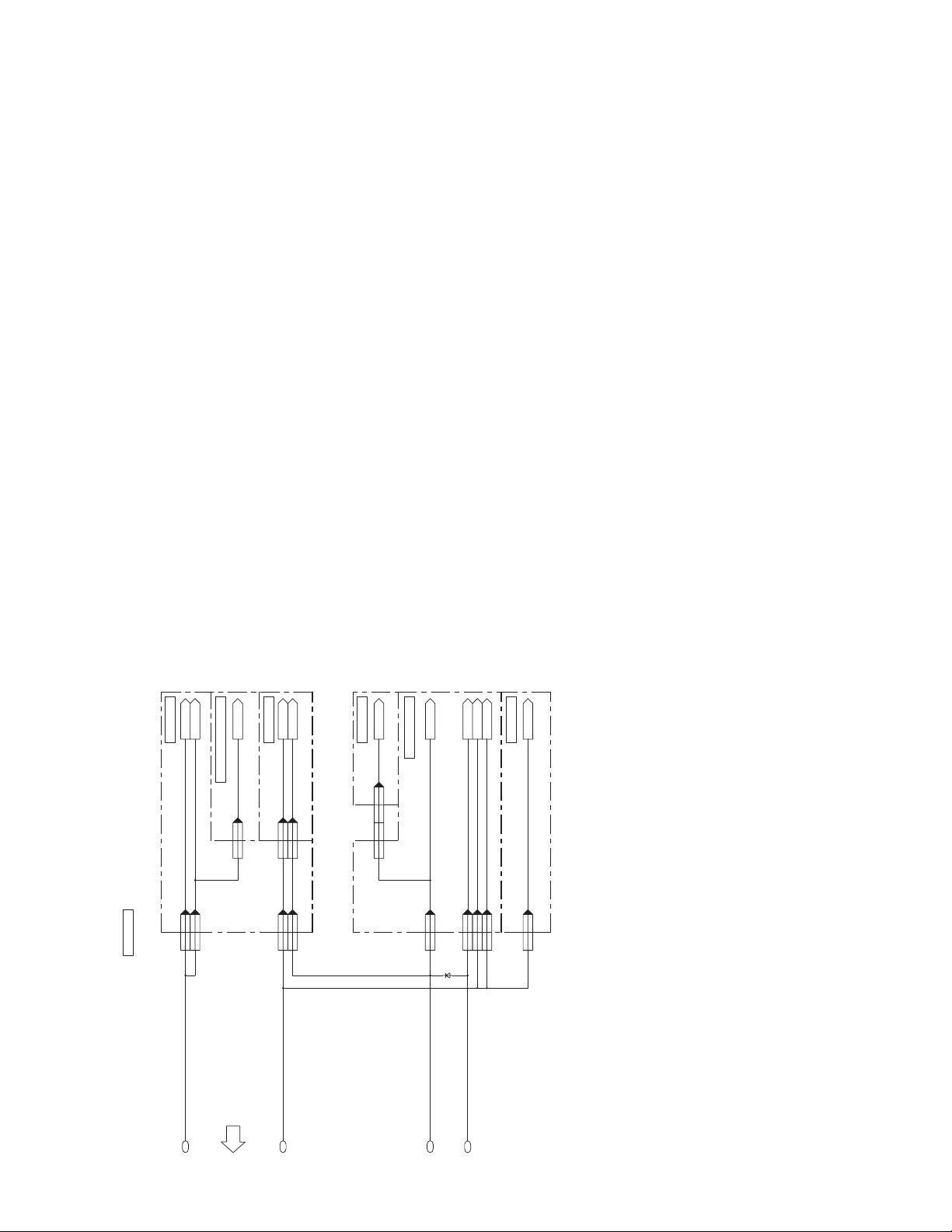
SA-AKX14 POWER SUPPLY (2/2) BLOCK DIAGRAM
72
MAIN P.C.B.
3.3V
DVREF
PANEL P.C.B.
DVREF+ DVREF+
SYS3.3V SYS3.3V
144
126
CN6001CN2003
CN6001CN2003
DVREF+
SYS3.3V
SYS3.3V,DVREF+
1
3.3V
3.3V
LCD P.C.B.
REMOTE SENSOR P.C.B.
CD3.3V
22
CN6006CN600533CN6000ZJ6002*
VREF+ VREF+ VREF+
CD3.3V
108
CN6001CN2003
CD 3.3VCD 3.3V CD3.3V CD3.3V
TO POWER SUPPLY
BLOCK (1/2)
2
+5V +5V
CN6000ZJ6002*
+5V
CN6001CN2003
+5V +5V
5V
11
162
VBUS
USB P.C.B.
VBUS
VBUS
4,52
ZJ6001*CN7901
4,5
CN2005
4
CN2001
VBUS
5V
CD SERVO P.C.B.
15,1612,13
CN7002CN2706
+5V+5V +5V 5V
D2018,D2019
D2020,D2021
3
7.5V
CN7002CN2706
CD+7.5VCD+7.5V +7.5V +7.5V
4
3.3V
3.3V
LDSW
TUNER P.C.B.
127
226
CN7002CN2706
CD 3.3V 3.3V 3.3V
1315
CN7002CN2706
LD SW LD SW LD SW
CN51CN2010
3.3V 3.3V 3.3V
55
Page 73
REMOTE SENSOR P.C.B.
E
SENSOR
321
PbF
IR6000
1
4
CN6006
(SOLDER SIDE)
ALBUM/TRACK
132
VR6002
1
4
CN6005
PbF
1
7
ZJ6002*
PbF
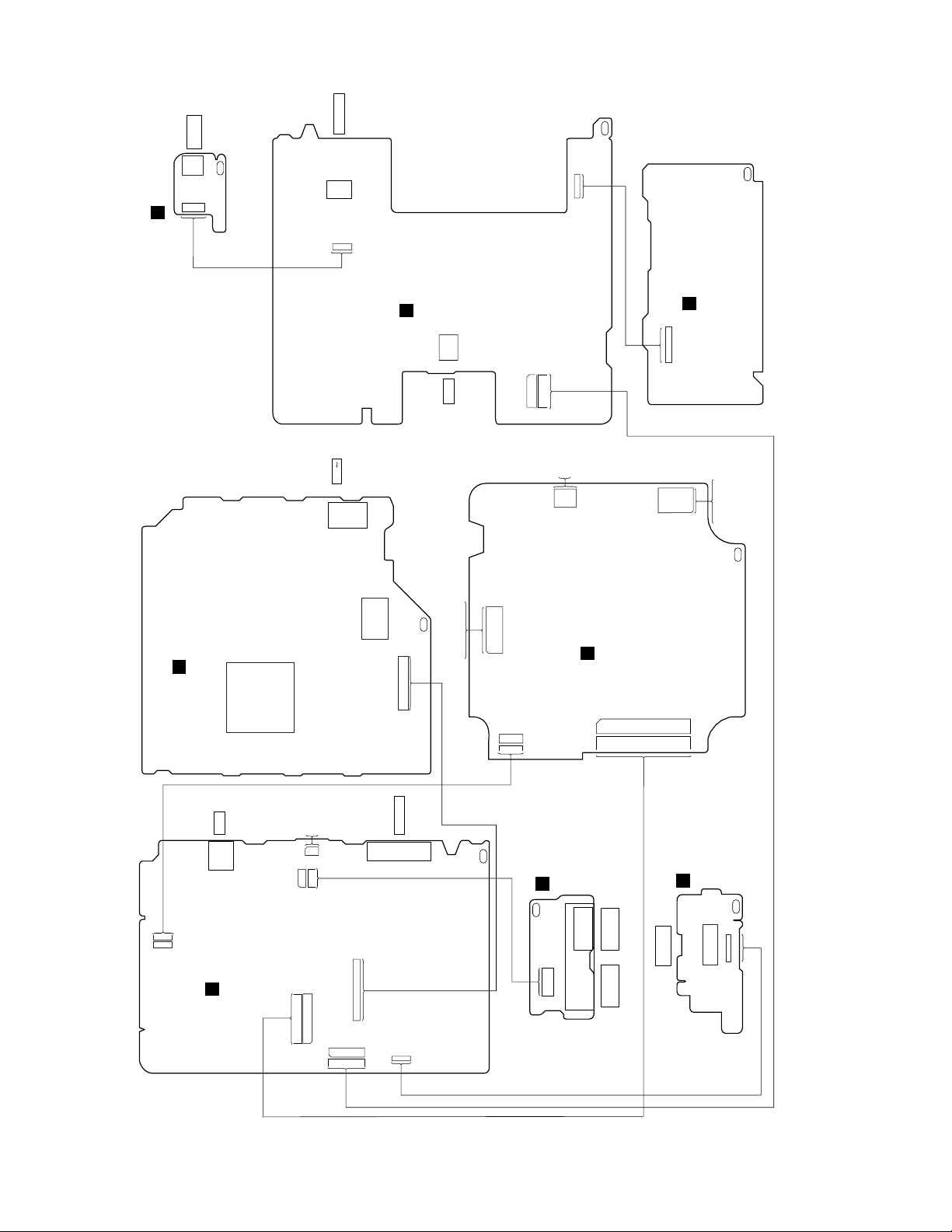
SMPS P.C.B.
H
PANEL P.C.B.
C
(SOLDER SIDE)
1 2 3
VR6001
1
2
16
17
VOLUME
AC IN
50/60Hz...PH
120V-60Hz...PN
110-127V/220-240V
P5701
T5751
PbF
10 9 8 7
1 2 3 4 5 6
(SUB TRANSFORMER)
(SOLDER SIDE)
T5701
456782
(MAIN TRANSFORMER)
1
019
16 15 14 13 12 11
1
15
CN5802
TO OPTICAL PICKUP UNIT
(CD MECHANISM UNIT BRS1C)
1 24
1
16
2
17
CN6001
FOR
DEBUG
5
1
CN7801*
CN7001
CD SERVO P.C.B.
A
(SIDE B)
2
1
1
5
1
5
CN7901
CN7002
27
26
LCD P.C.B.
D
(SOLDER SIDE)
1 7
CN6000
5
1
CN7003
TO LOADING
MOTOR PCB
(CD MECHANISM
UNIT BRS1C)
PbF
SA-AKX14 WIRING CONNECTION DIAGRAM
73
26
27
1
2
AUX IN
1
4
3
2
JK2000
5
1
1
5
CN2001
125
CN2002
9
2 8
CN2010
1
MAIN P.C.B.
B
(SOLDER SIDE)
1
27
2
26
26
2
27
1
16 Wiring Connection Diagram
FOR DEBUG
6
1
2 8
9
CN2706
CN2003
TO SPEAKERS
432
1
JK5000
115
CN2000
1
17
2
16
2
16
17
1
5
CN2005
1
PbF
TUNER P.C.B.
G
(SIDE B)
PbF
2 1
JK52
9
8
CN51
1
2
1
JK51
FM ANT AM ANT
USB PORT
USB P.C.B.
F
(SOLDER SIDE)
JK1111
432 1
5
6
PbF
51
ZJ6001*
NOTE: " * " REF IS FOR INDICATION ONLY.
Page 74
17 Schematic Diagram
17.1. Schematic Diagram Notes
s This schematic diagram may be modified at any time
with the development of new technology.
Notes:
S5701: Voltage ADJ switch (For PH only).
S6001:
S6002: D.BASS switch.
S6003: Manual EQ switch.
S6004: Rewind ( / ) switch.
S6005:
S6006: Album/Track switch.
S6007: USB switch.
S6008: CD switch.
S6009: Radio/EXT-IN switch.
S6010:
S6011: Stop ( ) switch.
S6012: Latin Preset EQ switch.
S6013: Open/Close switch ( ).
S7201: Reset switch.
VR6001: Volume Jog .
VR6002: Album/Track Jog.
s Important safety notice:
Components identified by mark have special characteristics important for safety.
Furthermore, special parts which have purposes of fire-retardant (resistors), high quality sound (capacitors), low-noise
(resistors), etc are used.
When replacing any of components, be sure to use only
manufacturer’s specified parts shown in the parts list.
Power switch ( ).
Forward ( / ) switch.
Play/Pause ( / ) switch.
s In case of AC rated voltage Capacitors, the part no. and val-
ues will be indicated in the Schematic Diagram.
AC rated voltage capacitors:
C5700, C5
C5708
s Resistor
Unit of resistance is OHM [ ] (K=1,000, M=1,000,000).
s Capacitor
Unit of capacitance is F, unless otherwise noted. F=Farads,
pF=pico-Farad.
s Coil
Unit of inductance is H, unless otherwise noted.
s
*
REF IS FOR INDICATION ONLY.
s Voltage and signal line
701, C5703, C5704 (For PH), C5705 (For PH),
: +B signal line
: -B signal line
: CD Audio input signal line
: AUX/Tuner Audio input signal line
: Audio output signal line
: USB signal line
: AM signal line
: FM signal line
74
Page 75
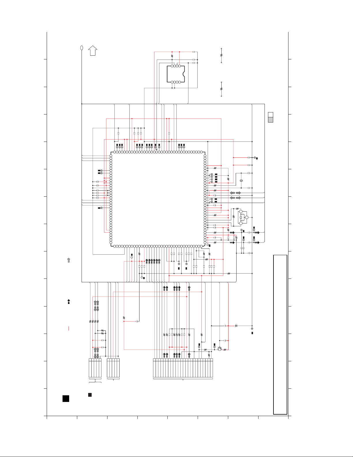
A
P1
B
3.3K
R7853
CIRCUIT (2/2)
TO CD SERVO
EE_DAT
EEPROM
IC7851
C3EBFC000042
6
EE_CLK
NC
3
0.01
C7851
330P
C7853
785
330P
C7852
WP
VCC
NCNCGND
214
0
K7013
0
K7003
EECLK
EECS
EEDATA
STATUS
MDATA
MCLK
USBDM
USB_SEL
: CD AUDIO INPUT SIGNAL LINE
33
34
94
USBDP
MLD
BLKCK
44TP45TP47
484645
47
49
IOVDD
iPod_CTRL_SW
MN16K_REQUEST_IN
MN947_REQUEST_OUT
RFIN
RFOUT
CENV
RFOENV
134
132
133
135
0.022C7107
3300PC7142
C7223 10
C7102 0.47
50
TP51TP
B
E
A
VTUNERARFDC
136
TP
44
iPod_DET
ARFOUT
137
C7161 0.1
5V
EECS
43
SRDATA
ARFFB
138
LRCK
[37] A11
[1] OUTL
ARFIN
139
C7216 680P
F
BCLK
[38] NRAS
[2] AVSS1
DSLF
140
C7244 0.015
0.1C7217
VSS
40424138373639
A10
NWE
A0
NCAS
A1
34 35
A2
DVDD
323029 31 33
DVSS
5.6KR7208
TEST1
PC
21
TP
MODEL_SEL
48
TP
iPod_PCONT
4
TP
27 282523212019 22 24 26
16.9344M CLK
IOVDD
MX2
1KR7205
MX1
DVSS
0R7151
USBDP
USBAVDD
0.1C7151
USBDM
32
USB_OE
31
USB_SEL
DVSS
0.1C7162
DVDD
IOVDD
DVDD
REGON
1KR7267
IOVDD
X2
X1
DVSS
0.1C7267
CSEL
0.1C7152
TEST0
OUTR
1KR7218
56312 4 131411 12 181615 1798710
AVDD1
AVREF
10C7236
1KR7217
1
PLLF
IREF
PLFO
VCOF
TL
142
141
144
143
820
2.7K
R7213
R7212
82K
R7211
0.01C7204
10C7208
1000PC7241
0.33C7213
0.082C7218
PD
10K
R7207
13
TP
TP
TP
100
R7221
0.01
C723010C7239
0
K7101
LD
LDSW
X7205
H0J120500076
470
R7214
1MR7220
X7201
H2D169500017
31
C7231
6.3V47
1000P
C7226
AGND
0.01
C7233
10
C7626
27P
C7206
27P
C7205
2
17
TP
67
TP
19
69
1
TP
TP
C7228
1
C7227
1000P
C7225
1000P
C7253
SA-AKX14 CD SERVO CIRCUIT
2/21/2
20
TP
USBDP
USBDM
USB_SEL
R_CH
L_CH
75
EECLK
EEDATA
DVSS
VREF
121
90
TP
59
TRCST / NC
TRCDO / NC
123
122
F
USBIN
VPPEX
TRCCLK / NC
IC7001
BBDDAACCEEF
125
124
F-
SCLK
SDATA
TP
USBIN
DEBUG-SCLK
DEBUG-SDATA
DEBUG-EXTGO
SERVO PROCESSOR
MN6627947RC
LDLDPDPDAVDD2
129
127
126
128
C
F+T-T+
C7264 0.1
51
50
DVSS
DVDD
AVSS2
130
131
3.3V
D
NRST
REST_SW
46
TP
6667626058565452535557
BA0
VDD3
IOVDD
RESTW
DO_UART_OUT/TX
DO_UART_IN/RX
[73] EECLK
NSTANDBY
NPWNDOWN
SRAMVDD2
SRAMVDD1
[107] A8
A3
TRVP
SPOUT
DVSS
114
113
115
112
TRVP
VREF
SPOUT
C7268 0.01
C7263 0.1
C7269 1
30TP29TP24TP28TP27TP26TP49TP52
616463
65
DVDD
VDD18
TRCD3 / NC
TRCD1 / NC
TRCD2 / NC
[74] EECS
[108] A7
TRP
FOP
OSCIN
CTRCRS
TRVP2
117
116
119
118
120
23
TP
R7111 10K
C7615 10
C7613 0.1
C7616 10
TRP
FOP
C7166 0.01
25TP71
TP
72
716968
70
TE
TX
NRST
EEDATA
CP_SCL
CP_SDA
TP
TP
TP
CP_RST
AMUTE
IOVDD4
C7163 0.1
8485 8081 77 7678 74 73757983 829394 9296 95 8990 87889199 9798 86
DVDD5
C7237 0.1
DVSS6
C7235 10
C7265 0.1
C7238 0.1
C7234 0.1
SREGOUT
SREGVDD
STATUS
MDATA
MCLK
REGION
D7
D6
D5
D4
D3
D2
D1
D0
DVDD
IOVDD
RAM_CLK
105 101102 100104 103106108
A9
107
A5
A4
A6
111
110
109
VSS
SCLK
NRST
SDATA
0
0.01
OCD_SCL
OCD_SDA
CN7801*
K7724
23154
VSS
NRST
STBY3.3V
FOR DEBUG
C7741
0.01
C7670
R7731 0
C7754 10
12
VCC(5V)
VREF (2.1V)
R7761 2.2M
63
64
TP
5.6
R7650
0
K7102
675
9
8
F
NC
NCNCNC
NC
GND
CD-LD
MD/LPD
134
2
LD-GND
TP
Q7601
LASER DRIVE
B1ADCF000001
C7601
R7601
10
4.7
R7702 0
R7712 0
R7721 0
R7717 0
R7707 0
C7755 10
C7753 10
C7752 0.01
D
NC
CD/DVD SW
1315141110
A
E
B
GND(PD)
21221816172019
24
23
F-
T-
F+CT+
D7650
DZ2J056M0L
16
TP
CN7001
TO
OPTICAL
PICKUP UNIT
(CD MECHANISM
UNIT BRS1C)
C
D
E
F
G
NOTE: “ * ” REF IS FOR INDICATION ONLY
H
Nota:
Para el valor y clave de cada componente referirse a; "Lista de partes Eléctricas" a partir de la página
102.
1 2 3 4 5 6 7 8 9 10 11 12 13 14
2 3 4 5 6 7 8 9 10 11 12 13 14
CD SERVO CIRCUIT
SCHEMATIC DIAGRAM - 1
1
A
: +B SIGNAL LINE : USB SIGNAL LINE
0R7911
1KR7896
USB_SEL
CN7901
TO
33R7902
33R7901
2311554
D-
D+
VBUS
USB_DGND
MAIN CIRCUIT
(CN2001)
IN SCHEMATIC
DIAGRAM - 6
B
R7904
R7903
C7902
C7903
15K
15K
10
0.01
7.2. CD Servo Circuit
Page 76
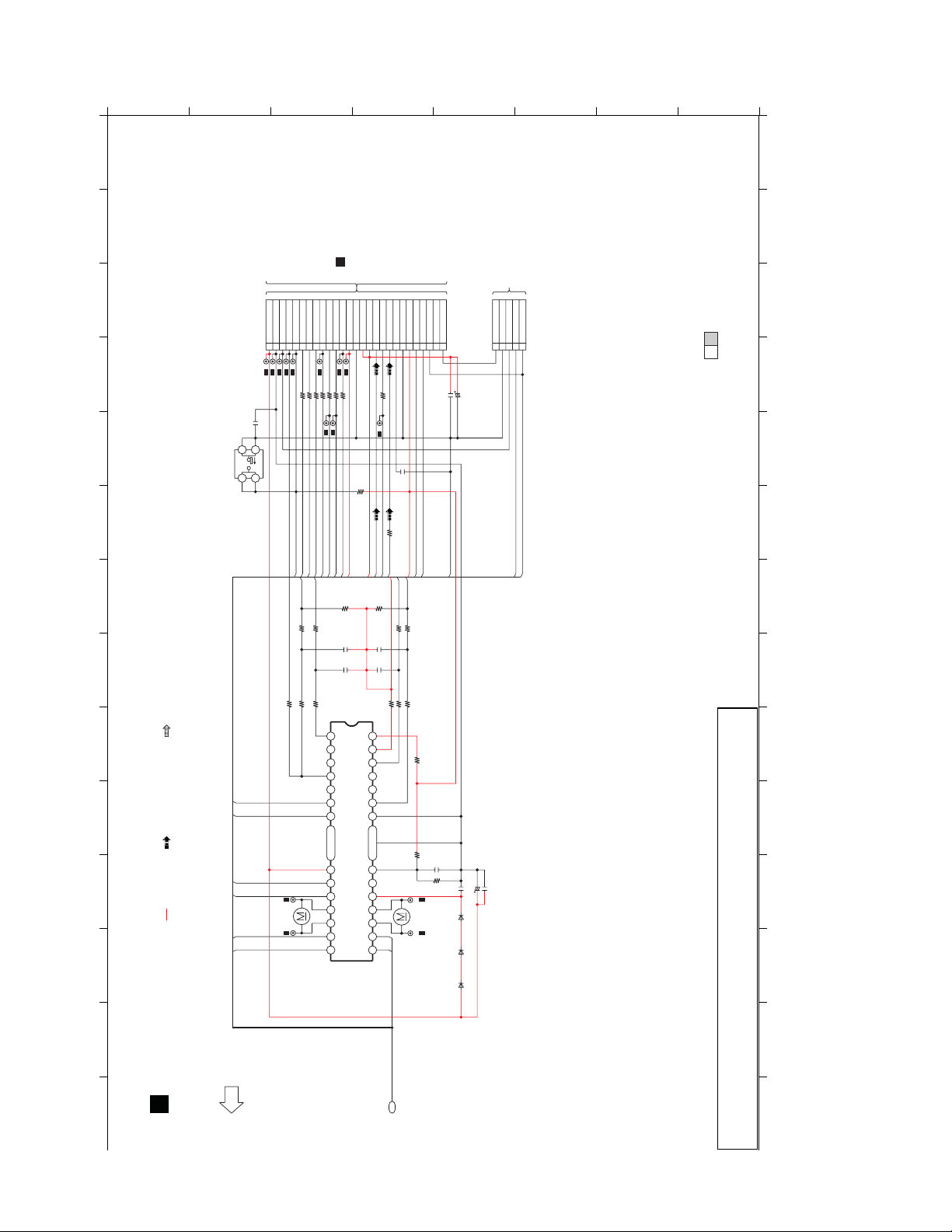
A
A
B
B
C
27
TO
MAIN CIRCUIT
(CN2706)
IN SCHEMATIC
DIAGRAM - 5
D
E
1
TO
F
LOADING P.C.B.
(CD MECHANISM UNIT BRS1C)
G
H
: CD AUDIO INPUT SIGNAL LINE: +B SIGNAL LINE : USB SIGNAL LINE
0.01
C7243
4
31
S7201
RESET
2
LID_RIGHT
LID_LEFT
M-
M+
T-
T+
CN7002
+7.5V
PGND
LOADING (TRAVERSE)
CD_OPEN_SW
CD_INNER_SW
CD_SI
CD_SO
CD_RESET
CD_S_REQ
CD_SCLK
3
38
M7302*
TRAVERSE
39
12KR7332
TP
TP
REST_SW
MOTOR
CD_MREQ
675
9
824
11
R7265 100
R7264 100
R7262 100
R7253 100
R7254 1K
R7266 100
8
TP7TP
BLKCK
NRST
STATUS
MDATA
MCLK
MLD
TRP
TRVP
100KR7349
47KR7331
5.6KR7327
3.3KR7323
2167298345
1013
+
14 12 911
1
11
TP10TP3TP1TP2TP9TP12TP14TP
LD_SW
CD_USB_IN
121310
K7202 100
LDSW
USBIN
5.6K
R7322
0.015
C7338
1200P
C7352
VINFC
TRB_1
REGO2
VINSL
REGO1
FWD
REV
GND
VCC
VOTR-
VOTR+
VOSL+
VOSL-
VOFC-
IC7002
C0GBY0000117
+5V
DGND
+5V5VAGND
ROUT
18
161415
17
K7712 0
18
TP
10K
R7255
AGND
R_CH
1.5K
R7321
0.15
C7315
1800P
C7339
MUTE
BIAS
VINTK
TRB_2
NC
VINLD
GND
22 233021 282724 25 26
GND
VCTL
NC
PVCC
191817 2015 16
VOLD-
VOLD+
VOTK-
VOTK+ VOFC+
5CH MOTOR DRIVER
LOUT
K7713 0
L_CH
VREF
10R7336
F-
F+
DGND
CD_I2S_MCLK
3.3VM+M-
201922
21
15P
C7704
3.3V
FOP
SPOUT
1KR7315
27KR7328
4.7KR7329
100R7325
R7341
+
LD_CW
LID_LEFT
LID_RIGHT
100R7335
1.2K
36
M7301*
MOTOR
SPINDLE
37
LD_CCW
TP
TP
2526232427
C7340
R7340
CD_CLOSE_SW
C7207 10
VSS
1000P
1K
C7341
D7343
D7342
D7341
C7751 6.3V47
10
C7334
10V100
B0ECKM000008
B0ECKM000008
B0ECKM000008
CN7003
SW_CLOSE
0.01
C7335
GND
23154
SW_OPEN
M-
SA-AKX14 CD SERVO CIRCUIT
LDM+
LDM-
M+
2/21/2
76
CD SERVO CIRCUIT
SCHEMATIC DIAGRAM - 2
15 16 17 18 19 20 21 22 23 24 25 26 27 28
TO CD SERVO
CIRCUIT (1/2)
P1
NOTE: “ * ” REF IS FOR INDICATION ONLY
Nota:
Para el valor y clave de cada componente referirse a; "Lista de partes Eléctricas" a partir de la página
102.
15 16 17 18 19 20 21 22 23 24 25 26 27 28
Page 77
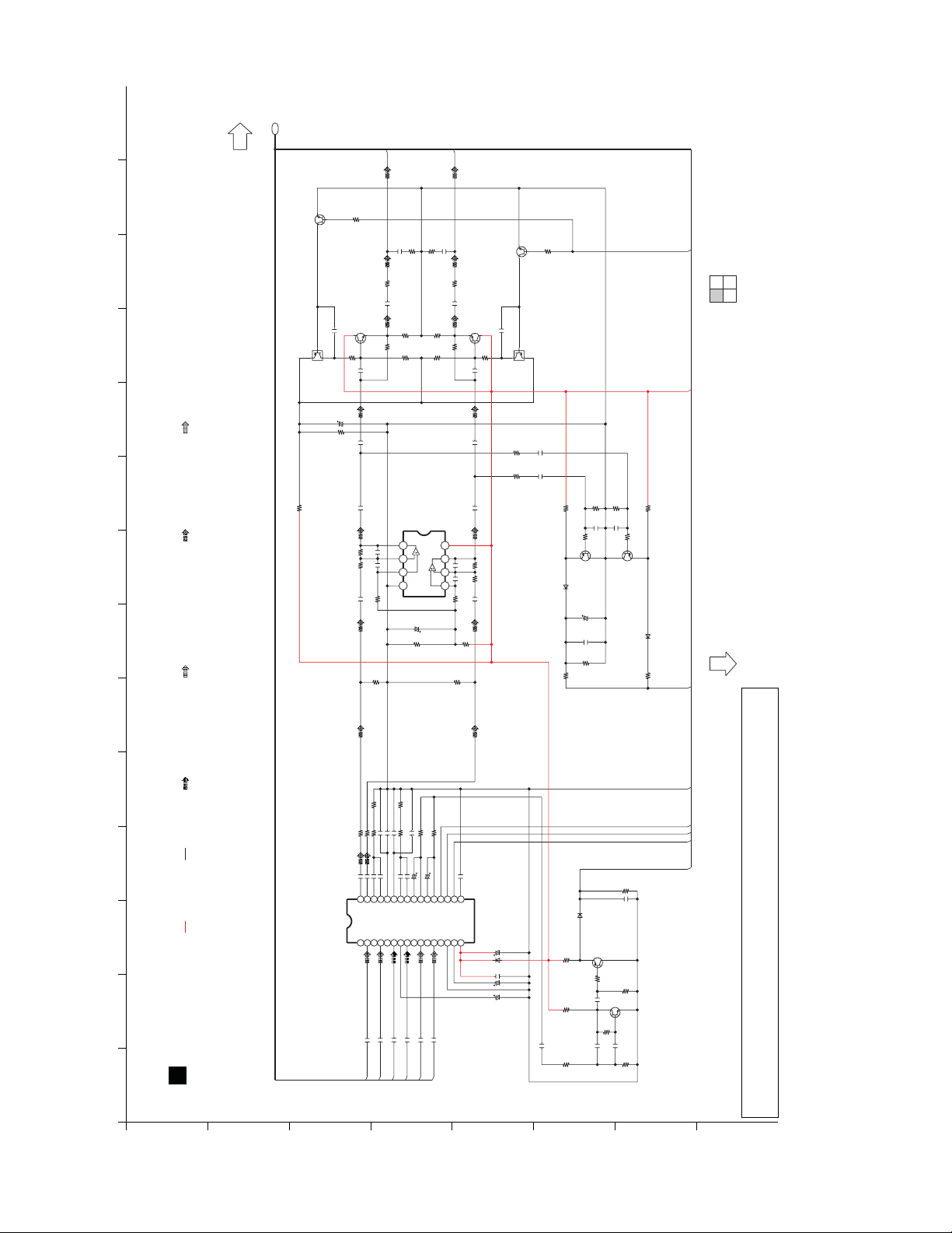
B
P1
: USB SIGNAL LINE
TO MAIN
CIRCUIT (2/4)
Q2040
B1ABCF000176
QR2400
B1GDCFJJ0047
2.2K
R2219
SWITCH
SWITCH
C2025
0.01
C2231
R2220
16V100
2.2K
R2372
Q2220
82K
R2223
C2221
C2220
C2405
R2208
R2205
C2209
FR
1K
10
C2222
BUFFER AMP
B1ABCF000176
2.7K
R2233
0.18
0.22
10
27K
560P
C2207
47P
4.7K
C2205
1
0
R2209
100K
R2313
R2302
C2307
100
0.1
R2222
R2230
1
24
3
330
R2305
4.7K
100K
V-
330
R2306
R2226
R2231
IC2201
DUAL OP-AMP
C0ABBB000067
V+
C2208
16V100
1K
R2201
FL
8.2K
R2347
D2301
DA2J10100L
100
R2376
BASS_SHIFT
+9V
CLIP_SENSOR
SA-AKX14 MAIN CIRCUIT
2/4
4/4
1/4
3/4
TO MAIN
CIRCUIT (3/4)
77
SWITCH
100
R2304
Q2222
B1ABCF000176
0.18
C2232
0.22
C2224
10
C2402
560P
C2206
47P
C2204
0
R2204
1K
R2202
100K
BUFFER AMP
82K
R2227
27K
R2207
4.7K
R2210
1
C2202
Q2041
0.1
C2308
10
C2226
4.7K
2.7K
R2225
100K
8
675
R2314
B1ABCF000176
0.01
C2026
SWITCH
QR2402
B1GDCFJJ0047
27K
R2349
C2007
27K
C2006
R2153
1K
R2374
0.068
0.068
8.2K
R2348
39K
39K
R2350
R2351
5600P
C2128
CLIP SENSING
R2131
5600P
C2138
Q2051
CLIP SENSING
B1ADCE000012
1K
D2300
DA2J10100L
100
R2377
1K
R2130
Q2050
B1ADCE000012
C2121
16V100
10
C2004
4.7M
R2121
: CD AUDIO INPUT SIGNAL LINE : AUX/TUNER AUDIO INPUT SIGNAL LINE : AUDIO OUTPUT SIGNAL LINE: -B SIGNAL LINE: +B SIGNAL LINE
AGND
330
330
R2114
R2111
UP_DGND
ASP_DATA
ASP_CLK
AUTO_BASS
Nota:
Para el valor y clave de cada componente referirse a; "Lista de partes Eléctricas" a partir de la página
102.
G
H
2 3 4 5 6 7 8 9 10 11 12 13 14
MAIN CIRCUIT
SCHEMATIC DIAGRAM - 3
1
A
2.2K
C2131 1800P
C2120 1800P
C2117 220P
C2112 220P
R2113 2.7K
R2307
R2308 2.2K
R2112 2.7K
R2016 47K
R2015 47K
4.7M
SWITCH
Q2039
B1ADCE000012
1K
R2359
1
C2248
470K
R2362
0.1
0.1
C2246
C2247
R2357
0.22
C2244
100K
R2360
SWITCH
Q2038
B1ABCF000176
2.2K
R2364
C2119 0.056
C2126 0.056
C2118 0.12
C2125 0.12
C2122 50V2.2
C2132 50V2.2
C2301 10
C2302 10
29
28
30
32
TREL
LOUTINR2
TRER
ROUT
ASP
IC2101
INR1
1
C1BB00001151
B
C
BASSR2INR3
INR5
INR4 BASSR1
231
5
4
3
C2109 1
C2113 1
AUX_R
TUN_R
BASSL2
BASSL1
DIFFG
DIFFL
DIFFR
726
825
627
10C2107
C2116 10
CD-L
CD-R
C2123 0.22
17
1815
202324
22
SCL
SDA
DGND
VOLINL
VOLINR
IGOUTL
IGOUTR
INL3
INL5
INL4
VCC CEXT
AGND
INL2
INL1
REFIN
16
13
11910
12 21
14 19
C2108 1
C2114 1
AUX_L
TUN_L
D
16V10
50V4.7
0.01
E
B0EAKM000117
D2120
C2133 16V100
C2127
C2134
C2817
C2245
D2028
DA2J10100L
4.7K
R2358
10K
R2361
1
33K
R2363
F
17.3. Main Circuit
Page 78
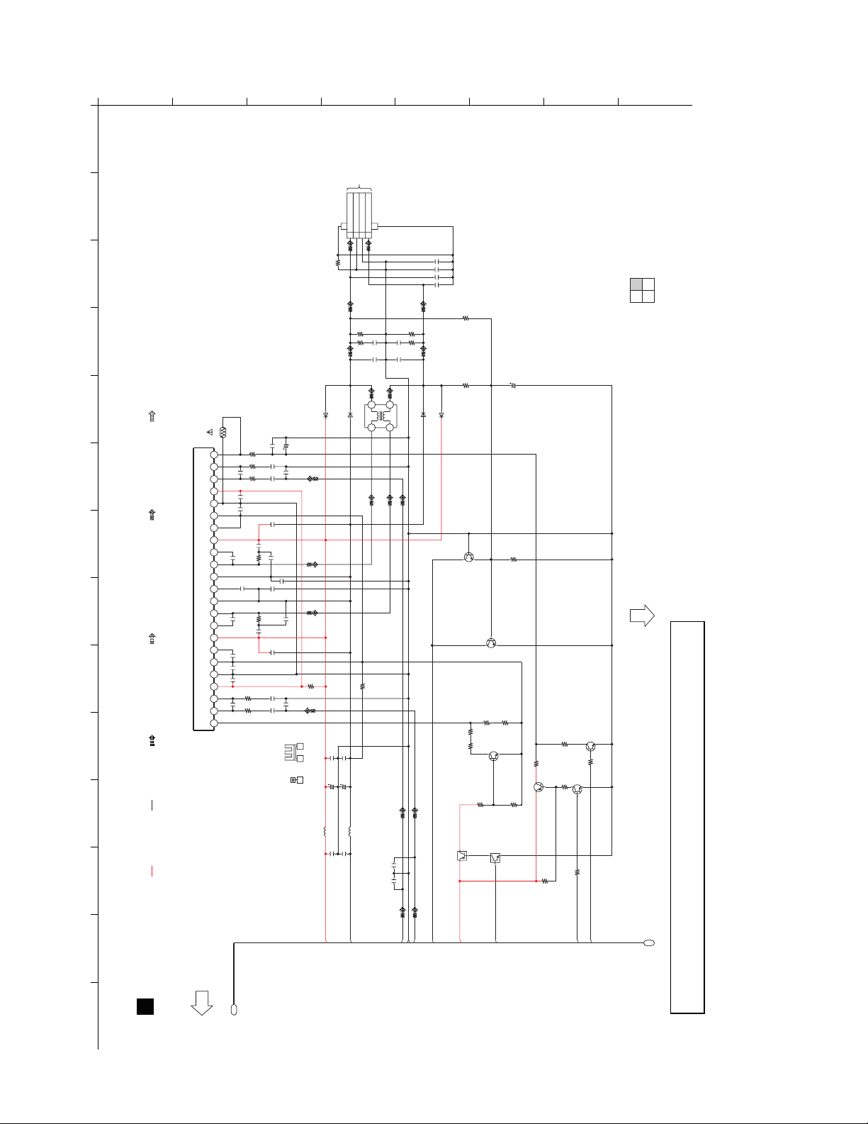
A
B
B
C
D
E
F
G
H
TO SPEAKERS
JK5000
RIGHT -
LEFT -G2LEFT +G1RIGHT +
423
1
: USB SIGNAL LINE
IC5902
: CD AUDIO INPUT SIGNAL LINE : AUX/TUNER AUDIO INPUT SIGNAL LINE : AUDIO OUTPUT SIGNAL LINE: -B SIGNAL LINE: +B SIGNAL LINE
TH5900
D4CC11040013
MODE
IN2+
IN2-
VDDA2
SGND2
19 21 23222010218974563121514 17 18161311
VSSA2
VSSD
VDDP2
BOOT2
OUT2
VSSP2
STABI
VSSP1
OUT1
C1BA00000497
AUDIO DIGITAL AMPLIFIER
BOOT1
VDDP1
PROT
VSSA1
SGND1
VDDA1
IN1-
IN1+
OSC
C5951
C5942
C5939
C5936
C5929
C5961
R5951
22 5.6K
R5947
D5908
B0EAKM000117
0.1C5802
D5906
B0EAKM000117
C5803 0.1
C5800 0.1
C5801 0.1
150K
R5962
150K
R5963
Q5905
B1ABCF000231
27K
R5911
180K
R5910
QR5900
B1GDCFJJ0047
C5946
10V100
6.8K
R5927
Q5904
SPEAKER PROTECTION SWITCH
B1ABCF000231
SPEAKER PROTECTION SWITCH
33K
1.5K
R5913
R5912
SWITCH
Q5900
120K
B1ABGC000005
R5907
10K
R5909
QR5901
+5V POWER SUPPLY
FREQUENCY HOPPING
B1GBCFJJ0051
2.7K
R5918
Q5901
B1ADCE000012
+5V VOLTAGE SUPPLY SWITCH
10K
R5914
Q5903
2.7K
R5920
10K
R5919
10K
R5917
Q5902
MODE SWITCH
B1ABCF000231
10K
R5915
SWITCH
B1ABCF000231
SA-AKX14 MAIN CIRCUIT
2/4
4/4
1/4
3/4
TO MAIN
CIRCUIT (4/4)
78
0
C5922
5.6K
R5950
0.1
0.1
22
C5994
C5993
R5946
0.47
0.47
C5990
C5989
2
43
D5910
D5909
L5903
1
G0A150L00003
B0EAKM000117
B0EAKM000117
50V1
1000P
C5983
C5985
100
R5942
0.47
5.6K
C5982
R5941
330P
C5980
0.1
C5973
0.1
C5970
C5964R5936
0.015
0.015
R5928
C5948
33P
0.1
0.1
5.6K
R5924
330P
5.6K
R5922
1000P
C5978
0.47
5.6K
C5976
R5939
C5968 0.1
220P
10
220P
C5962
C5958 0.1
C5954 0.47
0.1
C5956
10
220P
C5952
220P
C5943 0.1
R5926
L5901
J0JKB0000020
C5918
C5916
C5912
0.1
50V220
0.1
C5917
C5915
C5911
0.1
50V220
0.1
10
R5905
L5900
J0JKB0000020
C5902
C5901
1000P
1000P
0.47
C5931
0.47
C5925
HEATSINK*
RMCX1008*
C5927
10
1000P
G1G2
21
MAIN CIRCUIT
SCHEMATIC DIAGRAM - 4
15 16 17 18 19 20 21 22 23 24 25 26 27 28
TO MAIN
CIRCUIT (1/4)
+35V_SENSE
-35V_SENSE
P1
AGND
FL
FR
DC_DET_AMP
FHOP
+5V
MODE_DA
MUTE_F
P1
Nota:
Para el valor y clave de cada componente referirse a; "Lista de partes Eléctricas" a partir de la página
102.
NOTE: “ * ” REF IS FOR INDICATION ONLY
Page 79
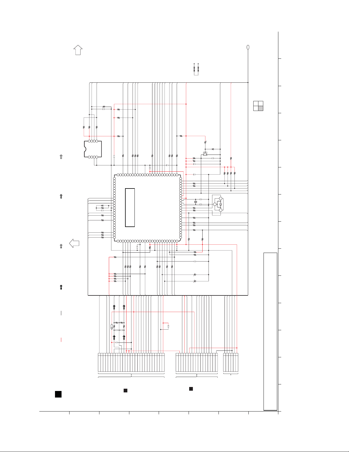
B
TO MAIN
A
C
CIRCUIT (4/4)
K2001*...PN
P1
K2002*...PH
: USB SIGNAL LINE
TO MAIN
: CD AUDIO INPUT SIGNAL LINE : AUX/TUNER AUDIO INPUT SIGNAL LINE : AUDIO OUTPUT SIGNAL LINE: -B SIGNAL LINE: +B SIGNAL LINE
4.7K
R2407
CIRCUIT (1/4)
R2408
EE_SCL
4.7K
LCD_CE
LCD_DATA
LCD_CE
LCD_WR
KEY2
CLIP SENSOR
AUTO BASS
959496
AUTO_BASS
CLIP_SENSOR
PGND
CD+7.5V
CD_S_REQ
100R2403
0.1
C2142
NC
LCD_DATA
CD_S_REQ
ROTARY JOG
REGION_AD
97
100R2071
ROTARY_JOG
DIMMER
100R2402
283231
DIMMER
VOL_JOG
98
100R2070
VOL_JOG
SMPS_ID
SYNC
1KR2196
NC
SMPS_ID
99
R2229
SYNC
232120 22
DC_DET_AMP
ASP_DATA
ASP_CLK
NRST
19171514 16 18
VDD1.8
VDD3.3
XO
XI
VSS
OSC1(IN)
OSC2(OUT)
MM0D0 (GND)
NC
10879 1211
REGION_CS
NC
PCONT
OCD_SCK
NC
OCD_SDA
465213
NC
VREF+
100
0.1
C2102
10K
DIMMER
SYS3.3V
DVREF+
VOL_JOG
6.3V1
0R2140
0R2136
100R2120
100R2117
4.7K
R2102
100KR2084
R2085
D2003
D2002
RMT
LCD_DATA
RESET
Q2011
B1GBCFLL0037
R2189 47K
C2144
C2137 0.1
C2130 0.1
R2129 100
R2126 100
H0A327200181
X2000
18PC2129
22PC2124
R2406 3.3K
R2197 100
4.7K
R2098
8.2K...PN
27K...PH
C2095 0.1
DZ2J033M0L
DZ2J033M0L
FL-GND
LCD_CE
LCD_WR
ROTARY_JOG
C2150
50V3.3
D2008
220
KEY1
KEY2
UP_DGND
DA2J10100L
C2139
47K
R2096
2
X2001
H2B800400007
31
NRST
MM0D0
47K
R2095
DVREF+
0
R2000
R2093 3.9K
OCD_SCK
R2094 3.9K
OCD_SDA
BASS_SHIFT
DC_DET_PWR
DC_DET_AMP
ASP_DATA
ASP_CLK
NRST
MM0D0
PCONT
OCD_SCK
OCD_SDA
SA-AKX14 MAIN CIRCUIT
2/4
4/4
1/4
3/4
79
CD_SI
100R2405
412439
42
NC
CD_M_REQ
[74] SMPS_BP
RMT
848385
1KR2076
RMT
CD_SI
CD_SCLK
382540
NC
VSS
CD_INNER_SW
IC2003
MICROPROCESSOR
*MN101EF16KXW
TU_INT
CLIP_ATTN
NC
868788
R2166 100
TU_INT
CD_SO
CD_MREQ
CD_RESET
CD_S_REQ
CD_SO
LCD_WR
CD_SCLK
1KR2404
0.1
C2141
373335
3429302726
36
CD_SI
CD_SO
VDD1.8
CD_SCLK
[25] NC
[24] BASS_SHIFT
[23] DC_DET_PWR
[1] NC
[2] NC
KEY1
VSS
VDD
NC
9091899392
10K
R2175
100R2066
R2067 100
KEY1
KEY2
CD_OPEN_SW
EE_CS
EE_SDA
R2235 22K
330PC2163
R2185
EEPROM
IC2006
C3EBEY000037
DA2J10100L
D2001
R2123 560K
10
C2115
R2011 1K
R2065 100
R2069 1K
100R2195
R2074 100
DVREF+
LD_CW
LD_CCW
R2017
CD-L
C2148
74 7172 6768 56 5558 57 52 5154 536566 6162 596064 6370 697375
2.2K...PH
1K...PN
R2182
R2232
0.022
50
NC
NC
NC
NC
NC
NC
NC
NC
VSS
NC
NC
NC
NC
NC
NC
NC
AGND
0
R2218
785
6
WP
SCL
SDA
VCC
GND
NC
NC
NC
2
431
EE_CS
EE_SCL
EE_SDA
LD_CW
LD_CCW
MODE_DA
FHOP
SMPS_BP
MUTE_F
CD_CLOSE_SW
CD_OPEN_SW
10K
10K
10K
R2198 1K
494748
NC
CD_OPEN_SW
EE_CS
EE_SCL
EE_SDA
CRTIMER
LD_CW
LD_CCW
MODE_DA
FHOP
NC
DC-DC ENABLE
78
R2174 10K
R2177 15K
R2173 15K
R2178 10K
DC ENABLE
CD-R
NC
797776
100R2156
TU_SDA
+5V
CD_USB_IN
45
NC
CD_USB IN
TU_SCLKNCNCNCTU_SDA
TU_RST
818280
R2164 100
R2159 100
TU_SCLK
TU_RST
CD_DGND
CD_MREQ
CD_RESET
CD_CLOSE_SW
1KR2163
R2165 1K
43
441346
CD_RESET
CD_CLOSE_SW
[50] NC
[75] MUTE_F
ecesita ser grabado
330P
C2103
CD_3.3V
CD_USB_IN
MAIN CIRCUIT
SCHEMATIC DIAGRAM - 5
I
6.8K
6.8K
R2105
R2107
J0JYC0000339LB2100
3.3K
3.3K
R2103
R2104
1000P
1000P
C2143
C2154
10
C2156
1
675
9
824
3
M-
M+
LD_CW
LD_CCW
CD_CLOSE_SW
CN2706
27
J
3.3V
DGND
CD_I2S_MCLK
K
121310
11
LOUT
ROUT
AGND
+5V
TO
+5V
CD SERVO
161415
DGND
LD_SW
CD_USB_IN
CIRCUIT (CN7002)
IN SCHEMATIC
DIAGRAM - 2
18
17
CD_SI
CD_SCLK
201922
CD_MREQ
CD_S_REQ
21
CD_SO
L
CD_RESET
CD_INNER_SW
LOADING (TRAVERSE)
2526232427
+7.5V
PGND
CD_OPEN_SW
1
C2157
10
658
9
7
214
NC
CN2003
17
M
3
+5V
DVREF+
DIMMER
VOL_JOG
SYS3.3V
RMT
TO
CD3.3V
LCD_DATA
PANEL CIRCUIT
(CN6001)
1112101415
FL-GND
LCD_CE
LCD_WR
IN SCHEMATIC
DIAGRAM - 7
13
KEY2
KEY1
ROTARY_JOG
17
16
NC
DGND
N
24316
5
VSS
MMOD
SYS3.3V
MICORST
OCD_SDL
OCD_SDA
CN2002
1
FOR DEBUG
NOTE: “ * ” REF IS FOR INDICATION ONLY
O
P
Nota:
Para el valor y clave de cada componente referirse a; "Lista de partes Eléctricas" a partir de la página
102.
1 2 3 4 5 6 7 8 9 10 11 12 13 14
Page 80
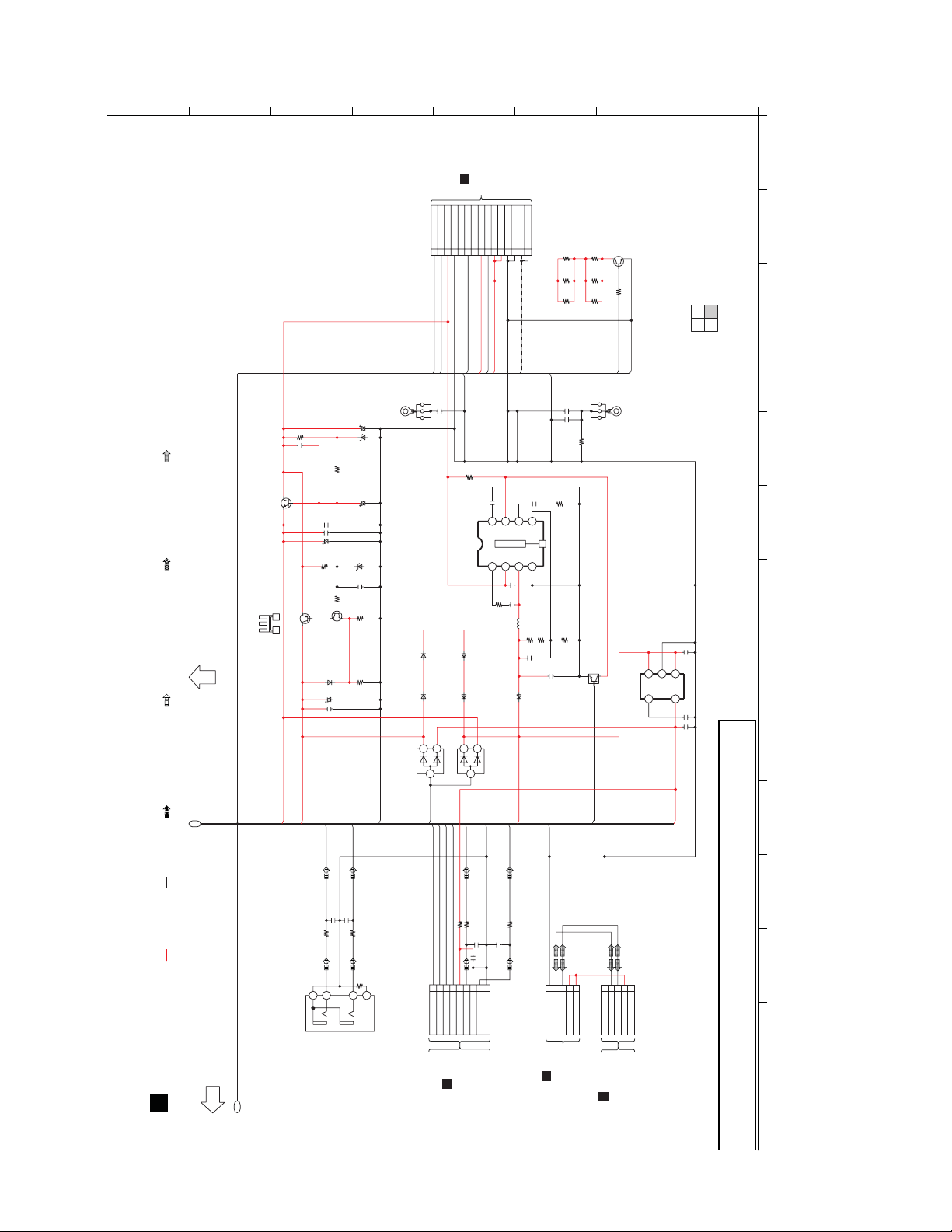
I
B
G
F
A
H
J
K
L
M
TO
SMPS CIRCUIT
(CN5802)
IN SCHEMATIC
DIAGRAM - 9
N
O
P
: USB SIGNAL LINE
TO MAIN
CIRCUIT (2/4)
Q2021
B1BACG000048
G2G1
HEATSINK*
R2029 180
0.01
C2105
+9V VOLTAGE REGULATOR
0.01C2203
16V220C2198
Q2022
B1BCCG000023
+7.5V VOLTAGE REGULATOR
100
R2028
C2104 0.01
680
R2278
100
R2271
Q2000
B1ABDF000026
DA2J10100L
D2000
C2234
25V220
D2004
DZ2J100M0L
C2106
16V100
DZ2J07500L
D2017
0.1
C2191
1K
R2010
VOLTAGE CONTROL
1K
R2018
C2188 10V100
C2187 0.1
CHASSIS
SCREW B
123
ZJ2001
D2018 D2019
B0EAMM000057 B0EAMM000057
D2014
B0ADDJ000032
CN2000
SMPS_ID
1
3
SMPS_ID
15
PCONT
C2218
2
PCONT
DC16V
131110
14
0.1
+16V_GND
12
D2020
D2021
D2015
B0ADDJ000032
SYS3.3V
TEMP_DET
ECO_CTL
DCDET2
8
9
SYS3.3V
DC_DET_PWR
SYNC
FL-GND
4.7K
R2234
0.1
C2236
IC2011
+5V SWITCHING
VOLTAGE REGULATOR
C0DBAYY01122
B0EAMM000057
B0EAKM000117
1
2
3
SYNC
+35V_SENSE
+35V_SENSE
8
SS
BST
1
R224022C2239
SYS_GND
SYS_GND
+35V_SENSE
576
4
7T15
EN
VIN
243
10
C2235
0.1
L2000
G0A330ZA0045
D2022
B0EAKM000117
-35V_SENSE
-35V_SENSE
231
-35V_SENSE
6
COMP
THERMALPAD
SW
R2237
C2240
C2237
FB
GND
56K
220P
Q2035
BEATPROOF SWITCH
B1BABG000007
470
470
R2338
R2339
470
470
R2336
R2333
UP_DGND
C2110
C2230
10K
6800P
R2236
1K
R2337
R2335
470
470
R2334
AGND
SMPS_BP
1000P
0.1
0
C2225
CHASSIS
321
SCREW A
ZJ2000
SA-AKX14 MAIN CIRCUIT
2/4
4/4
1/4
3/4
80
0
10K
R2238
R2239
SWITCH
C2238
QR2001
B1GBCFJJ0051
10
IC2009
C0DBFYY00049
+3.3V VOLTAGE REGULATOR
NC CE
312
4
10
C2201
VIN
VSS
VOUT
5
1
C2249
1
C2195
: CD AUDIO INPUT SIGNAL LINE : AUX/TUNER AUDIO INPUT SIGNAL LINE : AUDIO OUTPUT SIGNAL LINE: -B SIGNAL LINE: +B SIGNAL LINE
P1
MAIN CIRCUIT
SCHEMATIC DIAGRAM - 6
TO MAIN
CIRCUIT (3/4)
CD+7.5V
+9V
AUX_L
C2017
47K
R2001
1
2
[LCH]
JK2000
P1
100P
[RCH]
AUX IN
R2002
C2018
100P
47K
AUX_R
PGND
0
C2000
3
4
DC_DET_PWR
TUN_R
TU_INT
TU_RST
TU_SDA
TU_SCLK
0R2003
0LB2010
3267451
3.3V
R_OUT
TU_INT
TU_RST
TU_SDA
TU_SCLK
CN2010
9
TO
TUNER CIRCUIT
(CN51)
AGND
220P
C2015
1
C2003
8
GND
L_OUT
IN SCHEMATIC
DIAGRAM - 8
+5V
TUN_L
0R2004
220P
C2016
9
GND
CN2005
1
CD_DGND
23154
D+
DGND
TO
USB CIRCUIT
D-
VBUS
(ZJ6001*)
IN SCHEMATIC
DC_ENABLE
VBUS
DIAGRAM - 7
DGND
CN2001
5
TO
23154
D-
D+
VBUS
CD SERVO CIRCUIT
(CN7901)
USB_SEL
1
IN SCHEMATIC
DIAGRAM - 1
CD_3.3V
NOTE: “ * ” REF IS FOR INDICATION ONLY
Nota:
Para el valor y clave de cada componente referirse a; "Lista de partes Eléctricas" a partir de la página
102.
15 16 17 18 19 20 21 22 23 24 25 26 27 28
Page 81
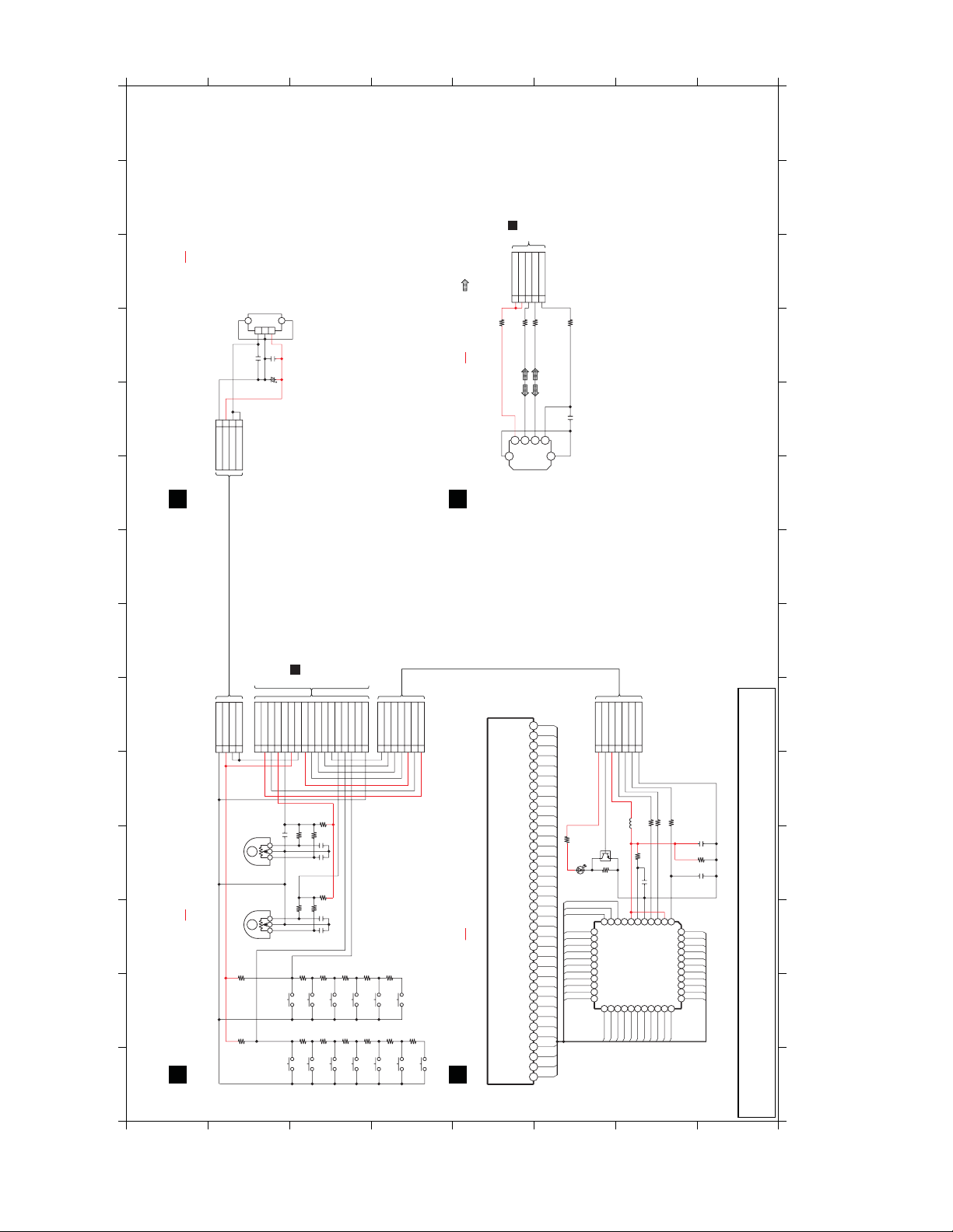
C
D
E
F
B
B
DGND
214
VREF+
3
RMT
RMT
B
IR6000
B3RAB0000084
REMOTE CONTROL SENSOR
G1
OUT
GND
VCC
213
100P
C6063
1000P
C6064
50V22
C6065
G2
A
CN6006
REMOTE SENSOR CIRCUIT
(CN2005)
IN SCHEMATIC
D-
D+
23154
DIAGRAM - 6
DGND
LB1210
F
0
G
H
C
D
E
: USB SIGNAL LINE
0
LB1200
TO
MAIN CIRCUIT
ZJ6001*
VBUS
VBUS
0
R12000R1210
: +B SIGNAL LINE
SA-AKX14 PANEL / LCD / REMOTE SENSOR / USB CIRCUIT
USB CIRCUIT
1
VBUS
G
G
JK1111
2
3
D-
D+
USB PORT
DGND
0.1
C1110
4
G
G
2 3 4 5 6 7 8 9 10 11 12 13 14
PANEL CIRCUIT
SCHEMATIC DIAGRAM - 7
1
CN6005
DGND
: +B SIGNAL LINE : +B SIGNAL LINE
VREF+
214
RMT
3
VR6001
VR6002
1
CN6001
RMT
VOLUME
EVEKE2F3524B
ALBUM/TRACK
K9AA012Y0004
10K
R6013
10K
R6012
17
+5VNCDIMMER
16
123 123
C6050
DVREF+
141513
1000P
S6006
S6001
TO
RMT
SYS3.3V
VOL_JOG
111210
22K
R6059
22K
R6068
R6006
S6007
ALBUM/TRACK
R6001
S6002
POWER
MAIN CIRCUIT
(CN2003)
IN SCHEMATIC
DIAGRAM - 5
LCD_CE
LCD_DATA
CD3.3V
LCD_WR
9
7
10K
R6060
12K
100P
R6058
C6052
100P
C6051
10K
R6070
12K
100P
R6067
C6060
100P
C6055
1.2K
1.5K
R6007
CD
USB
S6008
1.2K
1.5K
R6002
S6003
D.BASS
MANUAL EQ
ROTARY_JOG
FL-GND
658
KEY1
3
2.2K
R6008
S6009
RADIO/EXT IN
2.2K
R6003
S6004
REWIND
81
17
LCD
Z900
L5AYAYY00061
SEG31
SEG30
SEG29
SEG28
SEG27
SEG26
SEG25
SEG24
SEG23
SEG22
SEG21
SEG20
SEG19
SEG18
SEG17
SEG16
SEG15
SEG14
SEG13
SEG12
SEG11
SEG10
SEG9
SEG8
SEG7
SEG6
SEG5
SEG4
SEG3
SEG2
SEG1
SEG0
COM3
COM2
COM1
COM0
323016 2120 232218 19 2827 292524 261711 14 1512 1361089714523 31 34 363533
ZJ6002*
LCD_WR
FL-GND
LCD_CE
+5V
DIMMER
CD3.3V
LCD_DATA
NC
DGND
KEY2
4513276
214
: +B SIGNAL LINE
3.3K
4.7K
R6009
R6010
STOP
S6011
S6010
PLAY/PAUSE
FORWARD
R6005
S6012
4.7K
LATIN
PRESET EQ
6.8K
R6011
S6013
OPEN/CLOSE
LCD CIRCUIT
R6004
3.3K
S6005
SEG31
SEG30
SEG29
SEG28
SEG27
SEG26
SEG25
SEG24
SEG23
SEG22
SEG21
SEG20
SEG19
SEG18
SEG17
SEG16
SEG15
SEG14
SEG13
SEG12
SEG11
SEG10
SEG9
SEG8
SEG7
SEG6
SEG5
SEG4
SEG3
SEG2
SEG1
SEG0
COM3
COM2
COM1
COM0
CN6000
+5V
FL-GND
CD3.3V
LCD_DATA
DIMMER
LCD_WR
LCD_CE
4513276
Q900
LED DRIVE
B1GBCFJN0033
180
R935
978
11
10
1215 14 131820
COM1
COM2BZCOM0
SEG30
SEG29
SEG28
[12] COM3
1617
SEG27
SEG26
SEG25
19
SEG24
[21] SEG23
21
SEG19
SEG20
SEG21
24232625283032
SEG21
SEG20
SEG19
L900
J0JBC0000019
VDD
VLCD
[13] SEG31
IC900
[22] SEG22
C0HBA0000295
SEG16
SEG18
SEG17
27
SEG17
SEG18
SEG16
R906 0
15K
R901
0.01
C907
56312
4
VSS
DATA
[1] /CS
LCD DRIVER
[34] SEG10
SEG14
SEG15
29
SEG14
SEG15
R905 0
/WR
[44] SEG0
[35] SEG9
SEG13
SEG13
SEG12
/RD
SEG12
R903 470
SEG11
SEG11
332231
C901 1000P
R908 1K
C902 220P
SEG0
SEG1
SEG1
SEG2
SEG2
SEG3
SEG3
SEG4
SEG4
SEG5
SEG5
SEG6
SEG6
SEG7
SEG7
SEG8
SEG8
SEG9
35 37 42 44433938 414036
SEG10
34
NOTE: “ * ” REF IS FOR INDICATION ONLY
1 2 3 4 5 6 7 8 9 10 11 12 13 14
180
D993
R933
B3AFA0000131
COM0
COM1
COM2
COM3
SEG31
SEG30
SEG29
SEG28
SEG27
SEG26
SEG25
SEG24
SEG23
SEG22
Nota:
Para el valor y clave de cada componente referirse a; "Lista de partes Eléctricas" a partir de la página
A
B
C
D
E
F
G
102.
H
17.4. Panel, LCD, Remote Sensor & USB Circuit
Page 82
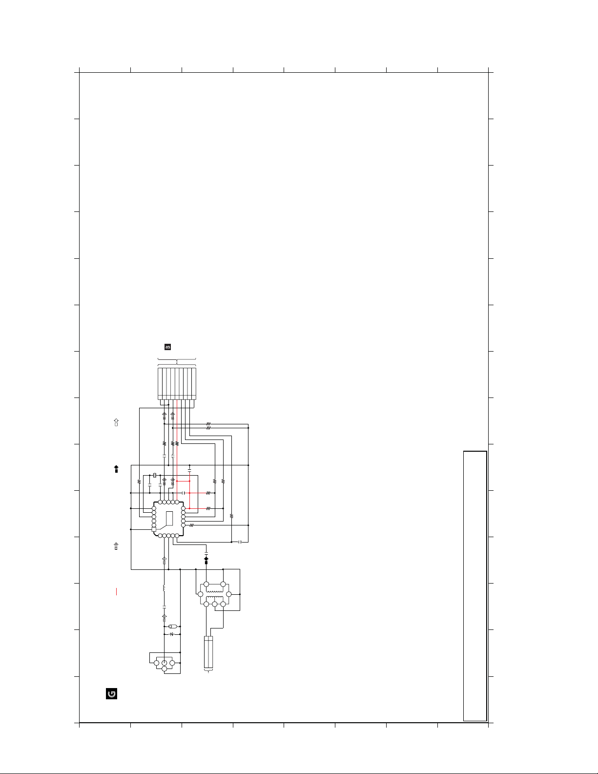
A
B
C
D
E
F
G
H
14
12 13
SA-AKX14 TUNER
B
TO
MAIN CIRCUIT
(CN2010)
IN SCHEMATIC
DIAGRAM - 6
9
1
CN51
3.3V
GND
GND
R_OUT
L_OUT
TU_RST
TU_INT
TU_SCLK
TU_SDA
3267451
9
8
7 8 9 10 11
R51 1K
R52 1K
L54 0
1
1
C59
12P
C58
IC52
H0A327200181
X51
12P
C57
15
DFS
LOUT
DOUT
DCLK
GCGPO2
GCGPO1
19 18
20
T1 17 16
NCNCFMI
1
2143134125
REP4780A
AM/FM RADIO RECEIVER
L51
G1CR18JA0020
C51
1000P
VA51
EZAEG2A50AX
C60
ROUT
PAD
THERMAL
RFGND
LB51
11
VDD
GND
AMI
RST
J0JBC0000032
C63
0.1
C61
VIO
1076
RCLK
9
SDIO
8
SCLK
SEN
6
: AM SIGNAL LINE : FM SIGNAL LINE
2.2K
R59
5
: TUNER AUDIO INPUT SIGNAL LINE
4
: +B SIGNAL LINE
2 3
G3
G1
JK51
G2
R61 47K
R62 47K
1
R64
0
L52
G2A380Y00002
220
220
R56
R55
R54
4.7K
R53
4.7K
R57 1K
0.1
C62
C52
0.47
4
6
G2
G1
231
1
2
AM ANT
AM ANT
JK52
7 8 9 10 11 12 13 14
6
5
4
82
17.5. Tuner
SCHEMATIC DIAGRAM - 8
1
A
TUNER CIRCUIT
G
FM ANT
B
AM ANT
C
H
Nota:
Para el valor y clave de cada componente referirse a; "Lista de partes Eléctricas" a partir de la página
102.
1 2 3
NOTE: “ * ” REF IS FOR INDICATION ONLY
D
E
F
G
Page 83
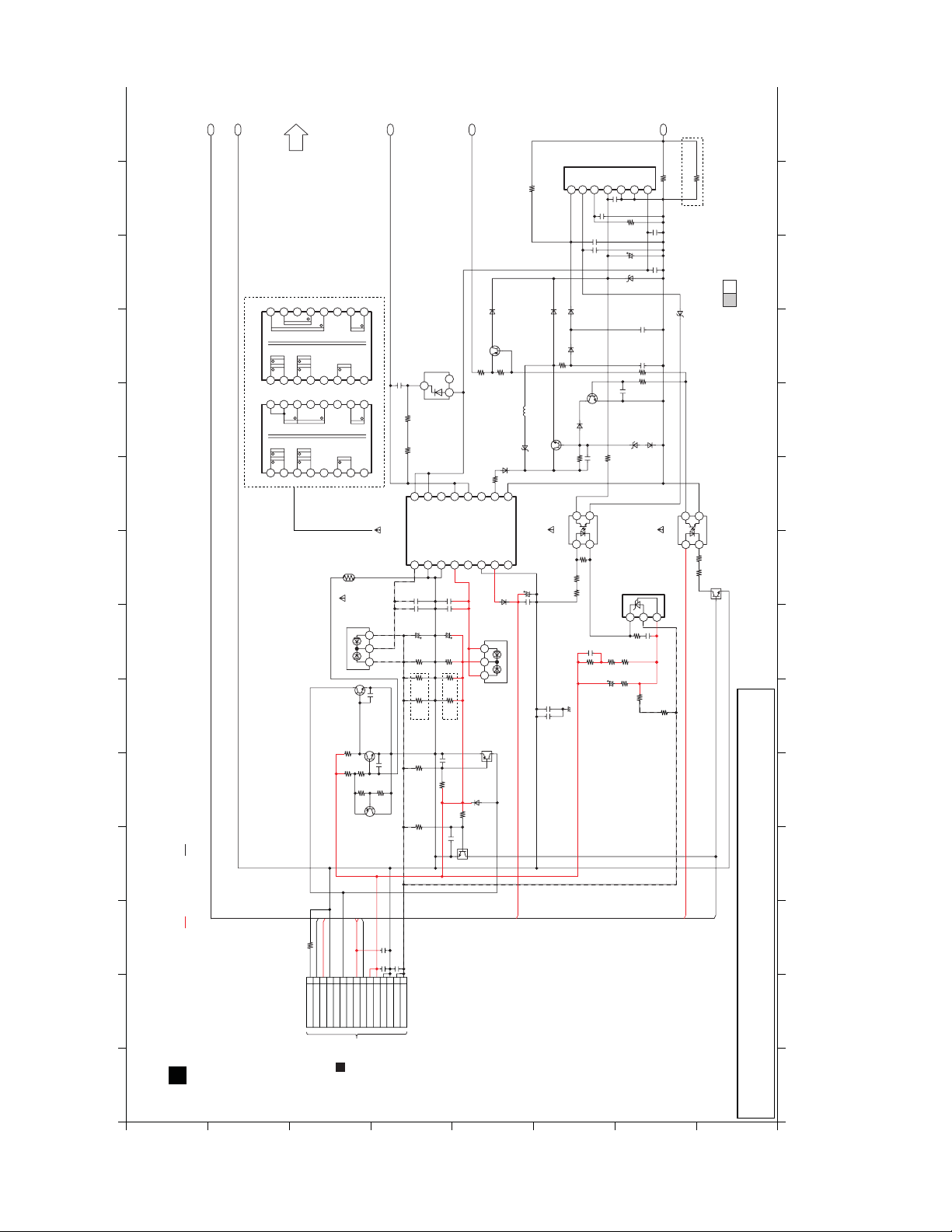
H
1
B
P1
2
3
4
: -B SIGNAL LINE: +B SIGNAL LINE
FOR PN
-35V
FOR PH
-35V
TO SMPS
CIRCUIT (2/2)
8
657
143
2
VIN
VCC
GND
D5726
B0EAKM000117
Q5721
R5732
SWITCH
B1ADCF000001
D5702
R5703
R5702
C5713
100K...PH
100K...PH
0.01
33K...PN
33K...PN
B0ZAZ0000089
21
3
8
657
GND
+35V
GND
+35V
131415
VIN
GND
131415
+12V
16
143
2
VCC
GND
+12V
16
9
111210
8
657
GND
9
111210
R5724
1K
120
R5723
L5704
J0JBC0000019
D5721
D5731
B0EAMM000057
B0BC01700015...PN
B0BC010A0007...PH
22
R5720
143
2
T5701
MAIN TRANSFORMER
G4DYZ0000057...PN
G4DYZ0000058...PH
9
TH5860
D4CC11040013
D5801
B0ABSM000008
Q5862
DC DETECT
B1GBCFJJ0051
18K
R5863
18K
R5862
R5861
R5860
312
0.1
C5869
Q5861
B1ABCF000176
TEMPERATURE DETECT
C5870
3.3K
10K
10K
R5864
Q5860
B1ADCF000001
TEMPERATURE DETECT
111210
C5820 0.01
C5821 0.01
C5805
C5808
50V680
50V680
2.2K
2.2K
R5834
R5832
2.2K
2.2K
R5835
R5833
2.2K
2.2K
R5836
R5837
FOR PH
FOR PH
10
R5841
R5800
C5843
120K
82K
R5840
22K
R5801
15K
10
C5844
0.1
131415
C5822 0.01
C5819 0.01
QR5802
D5804
SWITCH
QR5801
B1GBCFJN0038
16
B0HFRJ000012
D5802
312
B0ABSM000008
DC DETECT
B1GDCFGA0018
B0ACCK000012
C5813
C5812
IC5701
100
C5HACYY00004...PN
D5729
B0EAMM000057
Q5720
VOLTAGE REGULATOR
B1BABG000007
25V220
0.1
0.01
C5800
0.01
C5826
OCP/BD
SWITCHING REGULATOR
C5HACYY00005...PH
D5727
B0ACCK000012
D5724
1.2K
R5722
B0ACCK000012
Q5722
CURRENT
LIMITING SWITCH
B1ABCF000176
D5728
10K
R5721
4
PC5720
FEEDBACK
B3PBA0000579
1
2.2K
R5808
330
R5807
330
R5809
C5810
R5802
CHASSIS GND
OLP/SS
576
1
C5730
470P
C5723
0.1
C5725
B0ACCK000012
0.1
C5720
3
2
0.1
12K
S
GNDFBVCC
231
4
0.1
C5726
47K
R5733
50V56
C5724
D5732
C5728
1000P
1K
R5730
D5722
B0BC019A0007
IC5801
K
SHUNT REGULATOR
C0DAZYY00039
R5806
47K
1.5K
R5803
R5804
8.2K
C5817
R5814
100V0.1
C5722
C5721
15K
D
B0BC035A0007
1000P
220P
R5729 10K
R5728 100K
D5723
B0ACCK000012
A
R
0.1
C5818
2.2K
R5805
R5865
R5726
0.1...PH
0.15...PN
3300P
C5727...PN
820P
C5737...PH
D5725
B0BC6R100010
PC5701
FEEDBACK
B3PBA0000579
0
0.13
R5727
4
3
1
2
330
R5810
330
R5817
FOR PN
2/21/2
QR5810
PCONT SWITCH
B1GBCFLL0037
SA-AKX14 SMPS CIRCUIT
83
PW_DC+16V
PW_DC+16V
131110
14
DC16V
PCONT
12
ECO_CTL
+16V_GND
DCDET2
PW_SYS3.3V
8
9
SYS3.3V
TEMP_DET
SYNC
SYNC
C5896
C5831
576
4
SYS_GND
+35V_SENSE
+35V_SENSE
0.1
0.1
C5832
231
SYS_GND
-35V_SENSE
0.1
-35V_SENSE
PCONT
R5701
2.2K...PH
1K...PN
15
2 3 4 5 6 7 8 9 10 11 12 13 14
SMPS_ID
PW_SYS3.3V
PCONT
CN5802
SMPS CIRCUIT
SCHEMATIC DIAGRAM - 9
1
A
B
TO
MAIN CIRCUIT
(CN2000)
IN SCHEMATIC
DIAGRAM - 6
C
D
E
F
G
H
Nota:
Para el valor y clave de cada componente referirse a; "Lista de partes Eléctricas" a partir de la página
102.
1 2 3 4 5 6 7 8 9 10 11 12 13 14
17.6. SMPS Circuit
Page 84
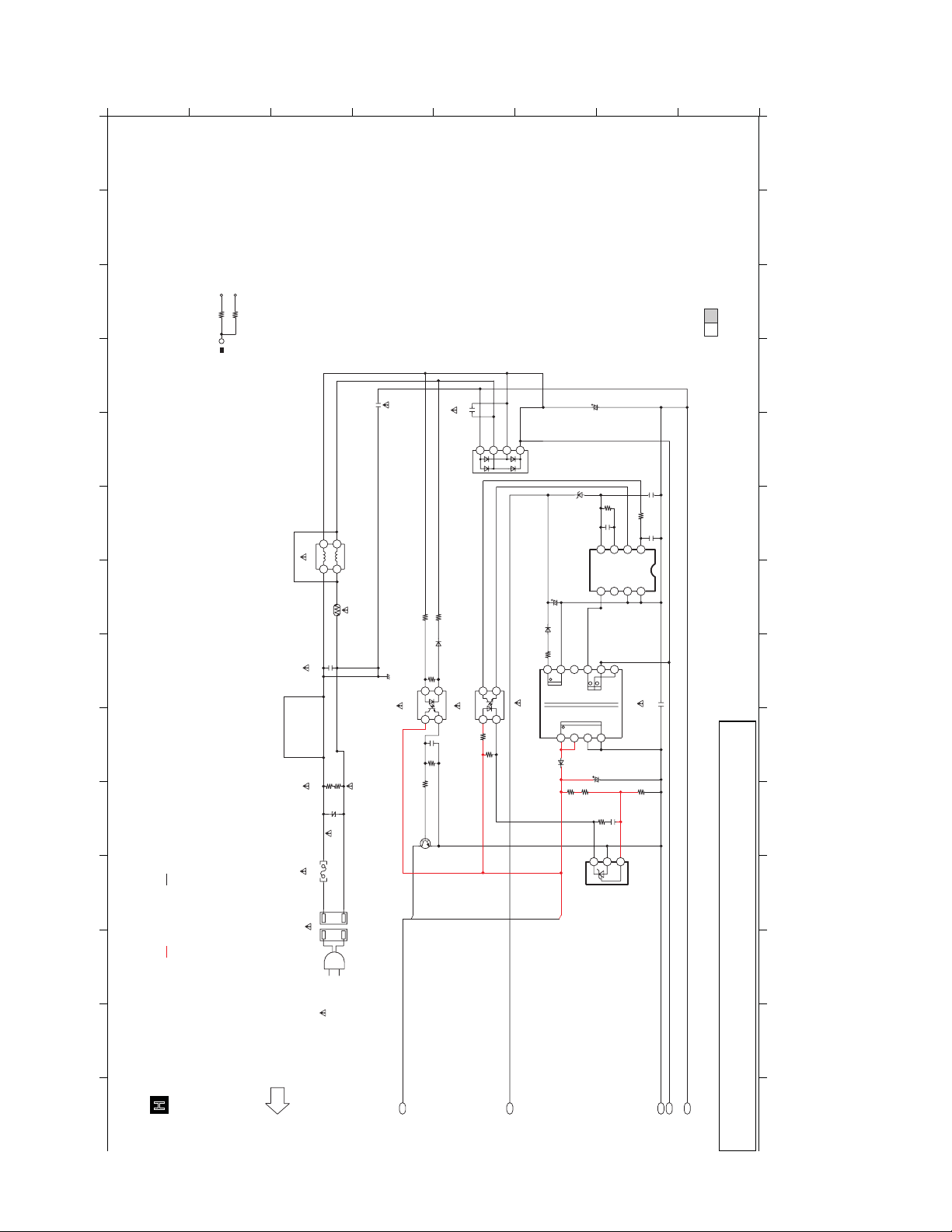
A
B
C
D
E
F
G
H
K1...PN0K3...PH
1
TP
0
SA-AKX14 SMPS CIRCUIT
2/21/2
25 26 27 28
470P
C5700
F1BAF471A013
23 24
1
L5705
2
34
G0B612H00004
: -B SIGNAL LINE: +B SIGNAL LINE
C5701
F0CAF104A105
R5708
ERJ8GEYJ155V
F1
0.1
8A 125V
TH5702
D4CAA2R20001
1.5M
1.5M
R5709
ERJ8GEYJ155V
DZ5701
ERZV05Z471CS
ZA5702
ZA5701
CHASSIS GND
220K
R5704
SYNC
PC5702
B3PBA0000579
100
R5897
SWITCH
Q5898
B1ABCF000176
SYNC
P5701
D5730
B0ECET000002
820K
R5706
1
4
0.1
C5897
100K
R5896
0.22
C5703
F0CAF224A105
321
4
D5701
B0EBNR000045
220K
R5705
2
4
PC5799
FEEDBACK
3
1
B3PBA0000579
150
R5894
2.2K
R5890
D5798
B0EAMM000057
22
R5798
3
2
18V
1575T
SUB TRANSFORMER
ETS19AB2E6AG
C5798
6
D5896
B0EAMM000057
25V220
5
3.3V
D5795
B0BC9R000008
IC5799
SUPPLY CONTROL
MIP2F20MSSCF
SWITCHING MODE POWER
3
4
9107
8
1K
10K
R5893
R5892
C5712
200V330
470K1000P
R5795
C5794
VCC
2
GND
C5899
10V220
15K
R5895
KAR
C5795
15K
R5797
243
FB
CL
VDD
S
SDNC
675
81
1
C5708
33K
R5891
0.1
C5898
1
0.1
C5796
1000P
F1BAF1020020
24 25 26 27 28
23
84
19 20 21 22
18
PW_SYS3.3V
IC5899
SHUNT REGULATOR
C0DAEYY00040
SCHEMATIC DIAGRAM - 10
15 16 17 18 19 20 21 22
SMPS CIRCUIT
H
TO SMPS
CIRCUIT (1/2)
AC IN
~127V 60Hz...PN
P1
3
124
NOTE: “ * ” REF IS FOR INDICATION ONLY
Nota:
Para el valor y clave de cada componente referirse a; "Lista de partes Eléctricas" a partir de la página
102.
15 16 17
Page 85
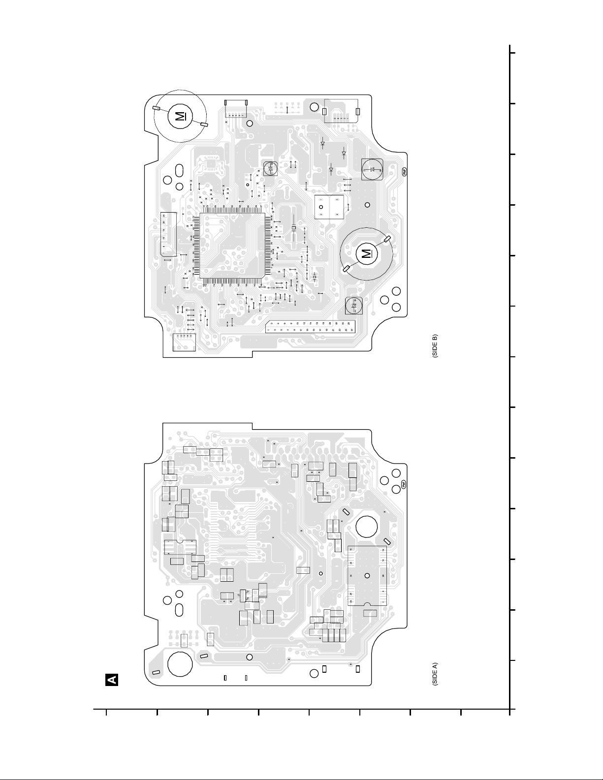
1+
CN7001
(TO OPTICAL PICKUP
(CD MECHANISM UNIT BRS1C))
M7302*
(TRAVERSE MOTOR)
C7741
K7102
R7911
CN7901
C7903
SA-AKX14
CD SERVO P.C.B.
D7342
1+
R7322
C7341
C7340
R7340
C7751
CN7003
(TO LOADING PCB
(CD MECHANISM UNIT BRS1C))
C7334
M7301*
(SPINDLE MOTOR)
2-
0707A-2
0707A-2
1
10 1 12 13
9
8
TP47
C7223
TP9
C7216
C7231
K7712
R7212
C7161
CN7002
R7208
C7218
C7244
C7162
TP20
K7003
D7341
R7341
R7335
TP21
R7207
TP48
X7205
TP4
R7205
TP32
TP31
R7267
R7218
TL1
C7239
C7226
R7213
C7253
R7217
C7213
C7225
R7211
C7217
C7241
K7101
C7152
R7896
TP18
C7236
C7206
C7205
C7616
C7151
R7214
R7220
R7151
S7201
(RESET SW)
X7201
D7343
C7267
CN7801*
(FOR DEBUG)
2-
TP52
TP49
TP24
C7166
K7202
TP46
TP29
TP25
TP30
TP71
TP12
TP33
TP34
C7163
R7761
TP94
TP7
C7237
C7265
TP8
C7902
R7903
R7265
R7901
R7253
R7902
R7266
R7904
C7263
TP13
R7111
C7613
TP26
TP28
TP27
IC7001
C7615
C7204
C7264
C7107
C7142
R7262
R7264
TP50
TP45 TP44
C7102
R7712
R7702
K7724
C7754
C7753
C7235
C7238
TP90
C7234
C7755
C7752
IC7851
C7851
K7013
CD SERVO P.C.B. (REPX0918C)
R7707
R7853
C7853
C7852
R7255
R7731 R7717
R7721
7
85
6
TP11
TP3
TP10
C7243
TP1
TP51
TP16
C7269
C7268
Q7601
C7208
C7601
R7601
C7670
D7650
C7230
TP38
R7650
TP64
TP63
R7254
C7207
TP14
TP2
TP67
R7221
C7228
TP69
TP23
K7713
R7321
R7327
TP17
TP19
C7227
R7332
R7315
R7349
C7352
C7315
C7704
C7626
C7233
TP36
R7331
R7323
C7338
R7328C7335
R7329
R7325
R7336
C7339
TP39
IC7002
0707A-2
0707A-2
TP37
5
4
3
2
18 Printed Circuit Board
18.1. CD Servo P.C.B.
NOTE: " * " REF IS FOR INDICATION ONLY.
1
H
G
F
E
D
C
B
A
Page 86
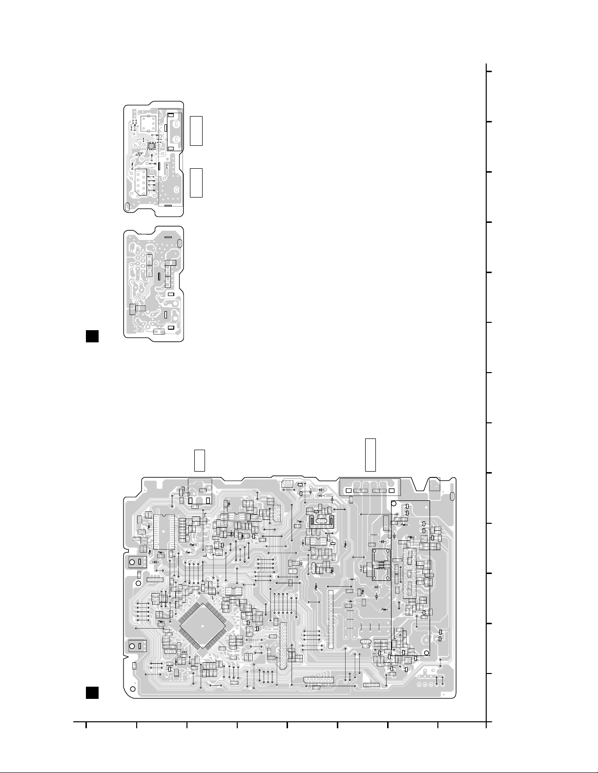
G
SA-AKX14
MAIN / TUNER P.C.B.
1
10 1 12 13
3559A
3559A
PbF
321
R53
R54
64
R56
R55
L52
C61
15
IC52
X51
C57
9
8
7
6
5
4
3
CN51
2
1
21
R64
R57
C62
6
10
11
5
1
16
20
JK52
C58
R59
VA51
C60
R52
R62
R61
AM ANT
1
FM ANT
JK51
3559A
3559A
PbF
R51
LB51
C59
C51
L51
C63
L54
TUNER P.C.B. (REPM12X141A)
C52
(SIDE A) (SIDE B)
9
8
86
7
6
AUX IN
12563
B
E
4
C
D2014
CN2002
(FOR DEBUG)
W5304
R2004
C2016
9
68
57
4
CN2010
3
K2000
2
1
W5077
W5061
W5058
W5311
K2013
C2249
45
IC2009
W5051
W5050
C2195
W5036
W5035
W5038
W5037
W5034
27
C2157
26
23 25
CN2706
22
21
W5305
20
16 18 24
14
31517191
R2104
12
11
10
9
8
C2156
C2154
R2107
7
C2143
6
5
4
3
2
1
W5011
W5010
W5003
D2020
E
C
B
D2021
D2015
W5076
C2188
C2187
ZA2000*
C2239
C2235
L2000
IC2011
C2201
W5046
3
2
1
D2022
W5039
R2105
R2103
357
1
2
CN2003
R2010
Q2000
E
R2018
C
Q2022
R2240
14
C2238
E
C
Q2021
B
C2234
W5027
W5026
W5028
W5025
W5029
468
JK5000
D2019
D2018
K2021
B
C2191
D2017
R2271
R2278
D2000
B
C
E
HEATSINK
W5092
C2236
R2234
C
58
E
B
QR2001
R2239
C2237
R2238
C2240
R2236
R2237
W5312
R2029
C2104
C2203
D2004
C2105
R2028
C2106
K2018
115
2
W5047
3
4
5
6
7
8
9
10
11
12
13
14
CN2000
9
151311
17
101214
16
W5309
W5004
W5078
1
32
C2113
C2109
C2107
4
29
C2817
7
26
C2116
23
10
IC2101
W5308
C2108
C2114
13
20
C2134
16
17
C2133
C2110
C2225
C2127
C2123
D2120
321
ZJ2000
C2230
12345
CN2001
W5041
W5080
W5081
W5082
W5083
1
32
ZJ2001
C2218
MAIN P.C.B. (REPM12X141A)
W5072
W5071
W5313
W5070
R2017
W5307
W5042
W5043
R2067
R2174
R2066
R2076
D2002
D2003
R2071
C2095
W5056
W5055
C2102
R2070
R2084
R2085
C2139
100
C2137
W5040
R2098
1
R2117
R2120
R2197
R2406
R2136
R2102
R2140
3
1
2
X2001
C2150
C2144
W5022
W5021
E
C
B
Q2011
W5020
D2008
R2002
1-GND
JK2000
4-GND
C2000
C2018
3-RCH
2-LCH
C2017
R2001
R2201
R2308
R2209
R2314
C2302
C2118
C2119
C2112
R2114
R2113
C2120
C2131
R2307
C2117
R2111
C2126
C2125
R2112
C2132
W5073
W5063
W5062
R2173
R2177
R2156
R2159
R2164
R2178
R2166
C2103
85
90
95
5
10
15
20
C2129
C2124
R2189
R2093
W5012
W5013
R2208
C2301
C2405
C2205 C2207
R2205
C2209
R2313
C2122
80
X2000
R2094
C2007
R2349
R2351
R2131
C2138
B
C
W5064
E
D2301
R2016
R2377
R2376
R2015
W5066
W5067
W5310
W5065
W5052
R2175
R2074
R2069
R2195
W5053
IC2006
75
76
R2065
R2011
70
65
60
55
IC2003
45
40
35
C2141
30
25
26
W5303
R2403
R2402
R2000
R2196
R2129
R2126
C2142
W5016
R2096
R2095
R2229
C2130
W5014
W5015
C2208
14
C2231
R2220
Q2051
W5068
14
C2148
C2115
D2001
R2123
51
50
W5017
W5018
W5069
R2235
C2163
R2198
R2163
R2165
R2219
C2004
W5085
R2405
R2404
IC2201
R2347
W5060
58
R2218
W5019
W5306
58
R2121
C2121
W5059
R2408
R2232
R2182
R2185
R2202
R2407
D2028
Q2039
W5075
R2204
C2202
R2207
C2206
R2210
C2402
C2003
C2015
R2003
C2204
LB2010
R2130
R2350
C2128
R2348
C2006
E
C
D2300
R2153
B
Q2050
W5048
W5089
W5090
W5088
W5087
W5086
W5049
W5054
R2361
W5033
R2358
W5032
R2363
R2357
C2245
C2244
C2247
R2364
C2246
R2362
B
C
E
B
C
E
R2360
R2359
C2248
Q2038
W5031
W5030
W5008
LB2100
W5302
W5301
W5091
W5084
W5079
W5009
W5007
B
18.2. Main & Tuner P.C.B.
H
G
F
E
D
TO SPEAKERS
B
C
E
B
C
E
Q5905
R5927
C5946
TH5900
R5942
23
15
15
R5913
C5901
C2308
R2306
E
B
C2224
Q2222
B
C
E
Q2041
2
1
ZA5903*
3533AA
3533AA
PbF
5
Q5904
Q5902
B
C
E
R5915
B
R5919
C
E
R5917
C5983
Q5903
R5920
E
C
R5918
B
R5914
Q5901
R5939
C5976
C5985
R5941
C5982
C5980
C5978
0222
C5973
C5964
C5970
C5961
R5936
C5962
R5911
R5912
10
2
C5929
R5924
R5910
W5024
R2231
R2227
C
QR2402
R5905
C5951
C5948
C5952
R5928
C5931
C5927
C5925
R5922
E
C
R5909
B
R5907
Q5900
QR5900
E
C
B
B
C
E
QR5901
HEATSINK
E
B
W5001
K2001...PN
K2002...PH
C5954
C5939
C5936
C2026
B
4
3
2
NOTE: " * " REF IS FOR INDICATION ONLY.
1
A
4-L-
3-L+
2-R-
1-R+
C5800
C5801
C5803
C5802
C5922
W5074
R5963
R5962
R5946
C5989
C5993
D5910
R5950
C2198
W5057
C5990
R5951
L5900
C5915
C5911
C5917
L5901
C5912
C5918
R2333
R2336
R2338
R2334
E
C
Q2035
K2020
W5005
K2019
W5006
CN2005
D5909
42
3
L5903
R5926
C5956
C5994
C5958
C5968
R5947
R2337
B
R2335
3
Q2220
W5045
1
C5943
D5908
C5942
IC5902
D5906
W5044
C5916
R2304
R2226
C5902
R2339
R2302
C2307
R2305
C2226
W5023
R2222
C2222
R2230
E
C
W5093
C
B
E
C
B
QR2400
R2225
C2232
C2221
R2223
R2233
R2374
C2025
C2220
E
C
B
R2372
Q2040
W5002
2
154
C
Page 87
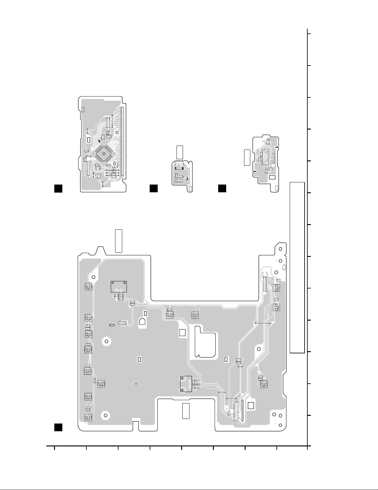
D
SA-AKX14
3533AC
3533AC
PbF
W906
R933
D993
22
16
R908
12
W905
IC900
11
5
L900
1
R901
C907
C901
1234 675
CN6000
LCD P.C.B. (REPM12X141A)
W910
W951
W952
W901
5363302520151051
Z900
W907
W909
W908
B
C
Q900
E
R935
R1210
R1200
1
2
3
4
JK1111
5
6
C1110
LB1210
2
3
4
51
ZJ6001*
LB1200
3533AD
3533AD
PbF
23
29
33
4
CN6006
SENSOR
33221
C6063
1
IR6000
C6064
C6065
3533AE
3533AE
PbF
USB PORT
USB P.C.B. (REPM12X141A)
F
34
40
R906
44
C902
W904
W903
R905
W902
R903
REMOTE SENSOR P.C.B. (REPM12X141A)
E
PANEL / LCD / REMOTE SENSOR / USB P.C.B.
1
10 1 12 13
9
8
S6006
(ALBUM/TRACK)
S6007
(USB)
(CD)
S6008
S6009
(RADIO/EXT IN)
S6010
(PLAY/PAUSE)
S6011
(STOP)
PANEL P.C.B. (REPM12X141A)
(OPEN/CLOSE)
S6013
R6005
R6006
R6007
R6008
R6009
R6010
R6011
S6012
(LATIN/EQ)
VR6002
C
ALBUM/TRACK
132
C6060
R6068
123
CN6005
7
3533AB
3533AB
PbF
1765432
W106
S6001
ZJ6002*
C6055
R6067
R6070
W108
W109
4
S6005
(FORWARD)
R6004
S6004
(REWIND)
(POWER)
R6001
S6002
(D. BASS)
W105
6
5
87
4
Nota:
Para el valor y clave de cada componente referirse a; "Lista de partes Eléctricas" a partir de la página
102.
R6013
R6012
VR6001
123
VOLUME
C6051
C6052
R6058
R6059
R6060
C6050
W102
R6002
R6003
W101
W110
1
2
3
4
5
6
7
8
9
10
11
12
14
5131
16
17
CN6001
W107
S6003
(MANUAL EQ)
3
2
NOTE: " * " REF IS FOR INDICATION ONLY.
1
18.3. Panel, LCD, Remote Sensor & USB P.C.B.
H
G
F
E
D
C
B
A
Page 88
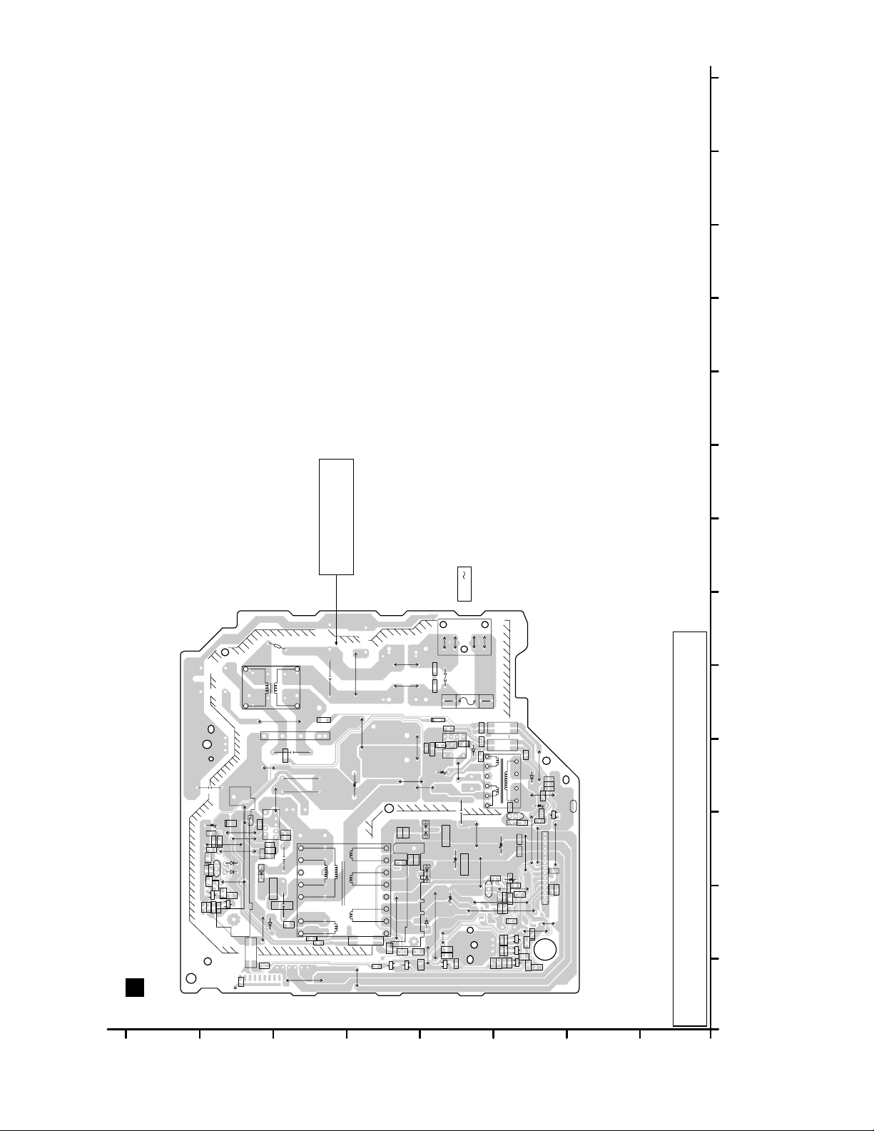
SMPS P.C.B.
SA-AKX14PH/PN
1
10 1 12 13
9
8
2
1
L5705
C5700
HEATSINK
W5527
D5732
C5724
D5721
C5720
R5721
D5723
B
E
Q5722
R5728
C5728
SMPS P.C.B. (REPM12X140A)
H
C5725
C5721
W5519
D5724
W5518
W5515
R5722
L5704
W5517
E
D5726
C
D5729
Q5720
B
D5702
W5516
D5722
R5724
D5728
C
B
C
E
R5729
R5723
Q5721
4
3
2
1
PC5701
K1
TP1
CAUTION
RISK OF ELECTRIC SHOCK
AC VOLTAGE LINE.
PLEASE DO NOT TOUCH THIS P.C.B
AC IN
120V 60Hz
7
88
6
W5532
W5531
W5530
C5821
TH5860
HEATSINK
R5807
C
QR5801
W5534
P5701
K5743
R5709
DZ5701
K5742
R5708
5
F1
D5730
ZA5702
ZA5701
8A 125V
R5797
2
3
1
4
D5795
C5794
R5795
K5711
C5796
C5795
8
7
5
D5798
IC5799
C5798
K5714
C5820
C5822
E
B
W5524
K5715
C5708
R5832
D5801
C5808
C5819
C5843
R5834
D5802
C5813
D5803
W5513
W5506
C5800
R5809
C5826
W5537
B
C
R5840
E
QR5802
W5525
R5706
W5601
R5798
W5514
21
43
6
5432
PRI
1
K
RA
IC5801
W5538
R5863
43
PC5702
21
PC5799
R5894
D5896
W5523
C5897
R5896
R5897
W5520
3568AA
3568AA
R5890
10 789
A
K
C5898
C5831 C5832
R5802
W5604
B
C
EB
C
E
B
C
E
Q5862
T5751
(MAIN TRANSFORMER)
R5893
R5895
W5521
W5522
W5511
C5817
W5510
W5602
CN5802
W5504
R5800
D5804
C5844
R5801
W5603
C5899
PbF
E
C
B
R5892
Q5898
W5512
C5896
C5812
R5701
15 14 13 12 11 10 1 2 3 4 5 6 7 8 9
W5540
W5505
SEC
R5891
R
IC5899
C5805
C5810
R5806
R5803
R5814
C5818
R5804
R5865
R5805
Q5861
R5841
C5870
R5860
R5861
Q5860
R5864
C5869
R5862
4
3
2
TH5702
3
4
W5541
-4
~3
~2
D5701
C5703
R5705
W5528
R5726
R5727
W5526
1
IC5701
32
4
C5726
C5730
5
6
R5733
7
R5732
D5727
C5723
T5701
C5722
C5727
(MAIN TRANSFORMER)
C5713
R5703
456782
R5702
R5720
D5731
W5509
1
R5810
W5533
C5701
R5704
+1
W5529
C5712
PRI
D5725
R5730
W5535
9
SEC
11 10
12
W5508
16 15 14 13
21
43
R5808
PC5720
E
R5817
C
B
QR5810
W5536
1
Nota:
Para el valor y clave de cada componente referirse a; "Lista de partes Eléctricas" a partir de la página
102.
18.5. SMPS P.C.B.
H
G
F
E
D
C
B
A
Page 89
19 Appendix Information of Schematic Diagram
19.1. Voltage & Waveform Chart
Note:
• Indication Voltage Values are in standard values for the unit measured by the DC electronic circuit tester (high-impedance) with
the chassis taken as standard.
Therefore, there may exist some errors in voltage values, depending on the internal impedance of the DC circuit tester.
• Circuit voltage and waveform described herein shall be regarded as reference information when probing defect point because it
may differ from actual measuring value due to difference of Measuring instrument and its measuring condition and product itself.
19.1.1. CD Servo P.C.B.
REF NO.
MODE 1234567891011121314151617181920
CD PLAY 1.5 0 3.3 3.3 1.7 0 0 0 1.7 1.5 3.3 1.6 1.8 3.3 1.8 0 1.8 0 1.8 3.3
REF NO.
MODE 21 22 23 24 25 26 27 28 29 30 31 32 33 34 35 36 37 38 39 40
CD PLAY 1.8 0 1.5 1.6 3.3 1.2 1.5 1.2 3.3 0 0 1.5 1.5 1.5 1.5 1.5 1.5 1.5 1.2 1.2
REF NO.
MODE 41 42 43 44 45 46 47 48 49 50 51 52 53 54 55 56 57 58 59 60
CD PLAY 3.3 3.3 3.3 0 2.1 0 3.3 3.3 3.3 0 3.3 3.3 3.3 0 3.3 3.3 1.2 1.2 1.5 0
REF NO.
MODE 61 62 63 64 65 66 67 68 69 70 71 72 73 74 75 76 77 78 79 80
CD PLAY 1.2 1.5 1.7 1.5 3.3 1.5 3.3 3.3 1.8 1.2 1.2 3.3 1.5 1.8 1.5 1.5 1.5 1.5 1.2 1.2
REF NO.
MODE 81 82 83 84 85 86 87 88 89 90 91 92 93 94 95 96 97 98 99 100
CD PLAY 0 3.3 3.3 3.3 3.3 0 3.3 3.3 3.3 1.5 3.3 3.3 3.3 0 1.5 1.5 1.5 1.5 1.5 1.5
REF NO.
MODE 101 102 103 104 105 106 107 108 109 110 111 112 113 114 115 116 117 118 119 120
CD PLAY 1.5 1.5 3.3 3.3 3.3 1.5 1.5 1.5 1.5 1.5 1.5 1.5 0 3.3 3.3 0 1.5 1.5 2.1 2.1
REF NO.
MODE 121 122 123 124 125 126 127 128 129 130 131 132 133 134 135 136 137 138 139 140
CD PLAY 2.1 1.5 1.5 1.5 1.5 1.2 1.5 1.8 1.8 0 3.3 3.3 3.3 3.3 3.3 3.3 3.3 3.3 3.3 3.3
IC7001
IC7001
IC7001
IC7001
IC7001
IC7001
IC7001
REF NO.
MODE 141 142 143 144
CD PLAY 3.3 3.3 3.3 3.3
REF NO.
MODE 1234567891011121314151617181920
CD PLAY 1.6 0 0 1.6 3.3 3.3 3.2 7.5 2.0 2.0 3.9 3.9 2.7 2.5 2.8 2.5 1.1 3.8 5.1 0
REF NO.
MODE 21 22 23 24 25 26 27 28 29 30
CD PLAY 1.5 0 1.1 0 0 1.6 1.6 3.2 0 0
REF NO.
MODE 12345678
CD PLAY00003.23.203.2
REF NO.
MODE E C B
CD PLAY 3.0 2.0 2.3
Q7601
IC7001
IC7002
IC7002
IC7851
SA-AKX14 CD SERVO P.C.B.
89
Page 90
19.2. Main P.C.B. (1/2)
REF NO.
MODE 1234567891011121314151617181920
POWER ON 0 0 0 3.4 0 1.2 3.3 0 0 0 0 1.6 1.6 0 1.1 1.8 3.3 1.8 3.3 3.4
STANDBY0003.401.23.300001.61.6001.83.31.83.33.4
REF NO.
MODE 21 22 23 24 25 26 27 28 29 30 31 32 33 34 35 36 37 38 39 40
POWER ON 3.3 3.3 3.3 2.8 0 1.7 0 3.3 1.1 0 3.3 0 3.3 3.3 3.3 3.3 1.8 3.3 0 3.3
STANDBY 3.3 3.3 3.3 2.8 0 1.7 0 3.3 1.1 0 3.3 0 3.3 3.3 3.3 3.3 2.0 3.3 0 3.3
REF NO.
MODE 41 42 43 44 45 46 47 48 49 50 51 52 53 54 55 56 57 58 59 60
POWER ON 3.3 0 0 3.3 0 3.3 0 3.4 0 0 0 0 0 0 0 0 0 0 0 3.4
STANDBY3.33.303.303.303.4000000000003.4
REF NO.
MODE 61 62 63 64 65 66 67 68 69 70 71 72 73 74 75 76 77 78 79 80
POWER ON 3.4 3.3 0 0 3.3 3.3 0 3.3 0 0 0 0 0 0 0 0 0 0 1.2 3.3
STANDBY3.43.3003.33.303.30000003.30001.23.3
REF NO.
MODE 81 82 83 84 85 86 87 88 89 90 91 92 93 94 95 96 97 98 99 100
POWER ON 1.2 0 0 0 3.3 0 3.3 0 3.4 0 0 3.4 3.4 0.5 1.0 1.8 1.4 2.3 0.7 3.4
STANDBY 1.2 0 0 0 3.3 0 3.3 0 3.4 0 0 3.4 3.4 0.5 1.0 1.8 1.4 1.5 0.7 3.4
REF NO.
MODE 12345678
CD PLAY00003.33.303.4
STANDBY00003.33.303.4
IC2003
IC2003
IC2003
IC2003
IC2003
IC2006
REF NO.
MODE 12345
POWER ON 4.9 0 5.2 0 3.1
STANDBY 4.9 0 5.2 0 3.1
REF NO.
MODE 12345678
POWER ON 9.7 12.9 5.2 0 0.5 1.6 12.9 2.7
STANDBY 9.7 12.9 5.2 0 0.5 1.6 12.9 2.7
REF NO.
MODE 1234567891011121314151617181920
CD PLAY 0 4.5 0 4.5 0 4.5 4.5 4.5 0 4.5 0 4.5 0 0 4.5 9 0 3.3 3.4 0
STANDBY 0 4.3 0 4.5 0 4.5 4.5 4.5 0 4.5 0 4.5 0 0 4.5 9 0 3.3 3.4 0
REF NO.
MODE 21 22 23 24 25 26 27 28 29 30 31 32
CD PLAY 4.5 4.5 4.5 4.5 4.5 4.5 4.5 4.5 4.5 4.5 4.5 4.5
STANDBY 4.5 4.5 4.5 4.5 4.5 4.5 4.5 4.5 4.5 4.5 4.5 4.5
IC2009
IC2011
IC2101
IC2101
SA-AKX14 MAIN P.C.B.
90
Page 91
19.3. Main P.C.B. (2/2)
REF NO.
MODE 12345678
CD PLAY 4.8 4.8 4.8 0 4.8 4.8 4.8 9.7
STANDBY 4.9 4.9 4.9 0 4.9 4.9 4.9 9.8
REF NO.
MODE 1234567891011121314151617181920
CD PLAY -11.0 0 0 34.5 0 -32.9 -24.6 35.6 0 0 -34.0 -31.0 -34.0 0 9.0 34.6 -34.0 -34.0 0 34.0
STANDBY -11.0 0 0 34.5 0 -32.9 -24.6 35.6 0 0 -34.0 -31.0 -34.0 0 9.0 34.6 -34.0 -34.0 0 34.0
REF NO.
MODE 21 22 23
CD PLAY 0 0 5.0
STANDBY 0 0 2.3
REF NO.
MODE ECB ECB ECB ECB ECB
POWER ON 7.0 7.0 7.7 0 3.3 0 9.7 16.0 10.3 16.0 7.9 7.0 0 34.5 0
STANDBY 7.0 7.0 7.7 0 3.3 0 9.7 16.0 10.3 16.0 7.9 7.0 0 34.5 0
REF NO.
MODE ECB ECB ECB ECB ECB
CD PLAY 0 1.7 0.6 1.4 0 0.8 0 0 0.7 0 0 0.7 0.8 0 0.2
STANDBY 0 1.7 0.6 1.4 0 0.8 0 0 0.7 0 0 0.7 0.8 0 0.2
REF NO.
MODE ECB ECB ECB ECB ECB
CD PLAY 0.8 0 0 0 9.7 3.4 3.4 9.7 3.9 -34.0 -27.9 -34.0 5.2 5.2 4.6
STANDBY 0.8 0 0 0 9.7 3.4 3.4 9.7 3.9 -34.0 -27.9 -34.0 5.2 5.2 4.6
Q2000 Q2011 Q2021 Q2022 Q2035
Q2038 Q2039 Q2040
Q2051 Q2220 Q2222 Q5900 Q5901
IC2201
IC5902
IC5902
Q2041 Q2050
REF NO.
MODE ECB ECB ECB ECB ECB
CD PLAY 0 0 0.7 0 3.4 0 0 3.3 0 0 3.3 0 5.0 12.0 0
STANDBY 0 0 0.7 0 0 0.7 0 3.3 0 0 3.3 0 5.0 12.0 0
REF NO.
MODE ECB ECB ECB ECB
CD PLAY 4.1 4.1 4.1 4.1 4.1 0 5.2 0 5.2 0 5.2 0
STANDBY 4.1 4.1 0 4.1 4.1 0 5.2 0 5.2 0 5.2 0
Q5902 Q5903 Q5904 Q5905 QR2001
QR2400 QR2402 QR5900 QR5901
SA-AKX14 MAIN P.C.B.
91
Page 92
19.4. LCD P.C.B.
REF NO.
MODE 1234567891011121314151617181920
POWER ON 3.3 3.2 3.3 3.3 0 2.9 3.3 0 1.4 1.4 1.4 1.5 1.4 1.4 1.4 1.4 1.4 1.4 1.4 1.4
STANDBY 3.3 3.2 3.3 3.3 0 2.9 3.3 0 1.4 1.4 1.4 1.5 1.4 1.4 1.4 1.4 1.4 1.4 1.4 1.4
REF NO.
MODE 21 22 23 24 25 26 27 28 29 30 31 32 33 34 35 36 37 38 39 40
POWER ON 1.4 1.4 1.4 1.4 1.4 1.4 1.4 1.4 1.4 1.4 1.4 1.4 1.4 1.4 1.4 1.4 1.4 1.4 1.4 1.4
STANDBY 1.4 1.4 1.4 1.4 1.4 1.4 1.4 1.4 1.4 1.4 1.4 1.4 1.4 1.4 1.4 1.4 1.4 1.4 1.4 1.4
REF NO.
MODE 41 42 43 44
POWER ON 1.4 1.4 1.4 1.4
STANDBY 1.4 1.4 1.4 1.4
REF NO.
MODE E C B
POWER ON000
STANDBY 0 0 3.3
Q900
IC900
IC900
IC900
SA-AKX14 LCD P.C.B.
19.5. Tuner P.C.B.
REF NO.
MODE 1234567891011121314151617181920
TUNER
01.503.0
0003.33.3
IC52
3.3 0 1.4 0.3 0 0 3.3 0 0 0
3.3
SA-AKX14 TUNER P.C.B.
92
Page 93
19.6. SMPS P.C.B.
REF NO.
MODE 1234567
POWER ON
STANDBY
REF NO.
MODE 12345678
POWER ON
STANDBY
REF NO.
MODE A K R
POWER ON 2.4 2.0 -30.0
STANDBY 2.4 2.0 -30.0
REF NO.
MODE A K R
POWER ON 1.2 0 0
STANDBY 1.2 0 0
REF NO.
MODE ECB ECB ECB ECB ECB
POWER ON 7.3 8.5 7.6 19.7 19.7 19.0 0 19.6 0 0 35.2 0 1.3 0 0.7
STANDBY 7.4 8.6 7.7 19.7 19.7 19.0 0 19.6 0 0 35.2 0 1.3 0 0.7
REF NO.
MODE ECB ECB ECB ECB ECB
POWER ON 0 0 0.7 0 3.3 0 0 3.1 0 0 3.3 6.6 0 0 3.1
STANDBY 0 3.3 0 0 3.3 0 0 3.1 0 0 3.3 6.6 0 0 3.1
164.8 0 0 19.1
164.8 0 0 19.1
5.9 1.0 2.3
5.9 1.0 2.3
Q5720 Q5721 Q5722 Q5860 Q5861
01.40.5
01.40.5
11.0 164.2 0 0 0
11.0 164.2 0 0 0
IC5701
IC5799
IC5801
IC5899
QR5802 QR5810Q5862 Q5898 QR5801
SA-AKX14 SMPS P.C.B.
93
Page 94
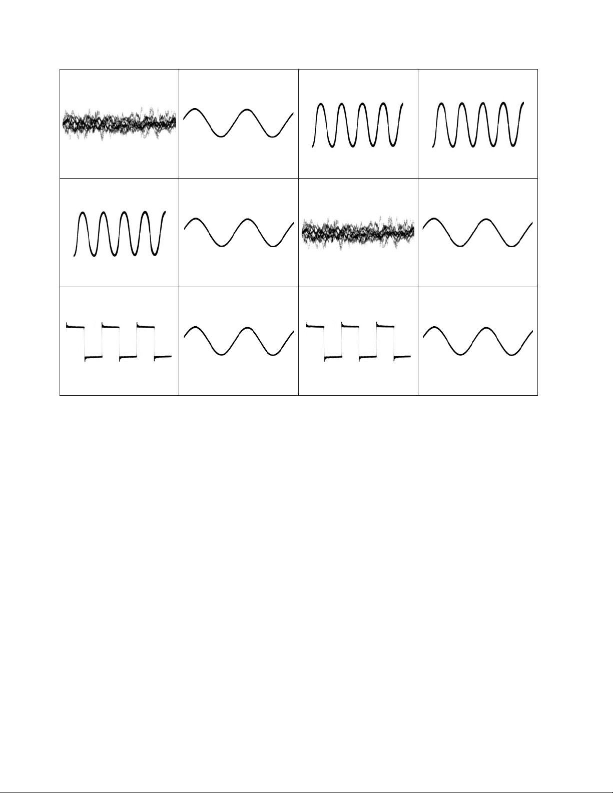
19.7. Waveform Table
WF No. IC52-2,13,14 (PLAY)
0.1Vp-p(200usec/div)
WF No. IC2003-15 (PLAY)
0.4Vp-p(200usec/div)
WF No. IC2101-31,32 (PLAY)
WF No. IC52-9,17 (PLAY)
0.2Vp-p(100usec/div)
WF No. IC2003-16 (PLAY)
2.95Vp-p(10usec/div)
WF No. IC5902-2 (PLAY)
WF No. IC2003-12 (PLAY)
4Vp-p(500usec/div)
WF No. IC2101-2,12 (PLAY)
0.1Vp-p(200usec/div)
WF No. IC5902-10,14 (PLAY)
WF No. IC2003-13 (PLAY)
3.2Vp-p(100usec/div)
WF No. IC2101-6,8 (PLAY)
1.4Vp-p(100usec/div)
WF No. IC5902-21 (PLAY)
3.6Vp-p(200usec/div)
1.4Vp-p(1msec/div)
100Vp-p(1usec/div)
1.5Vp-p(500usec/div)
94
Page 95
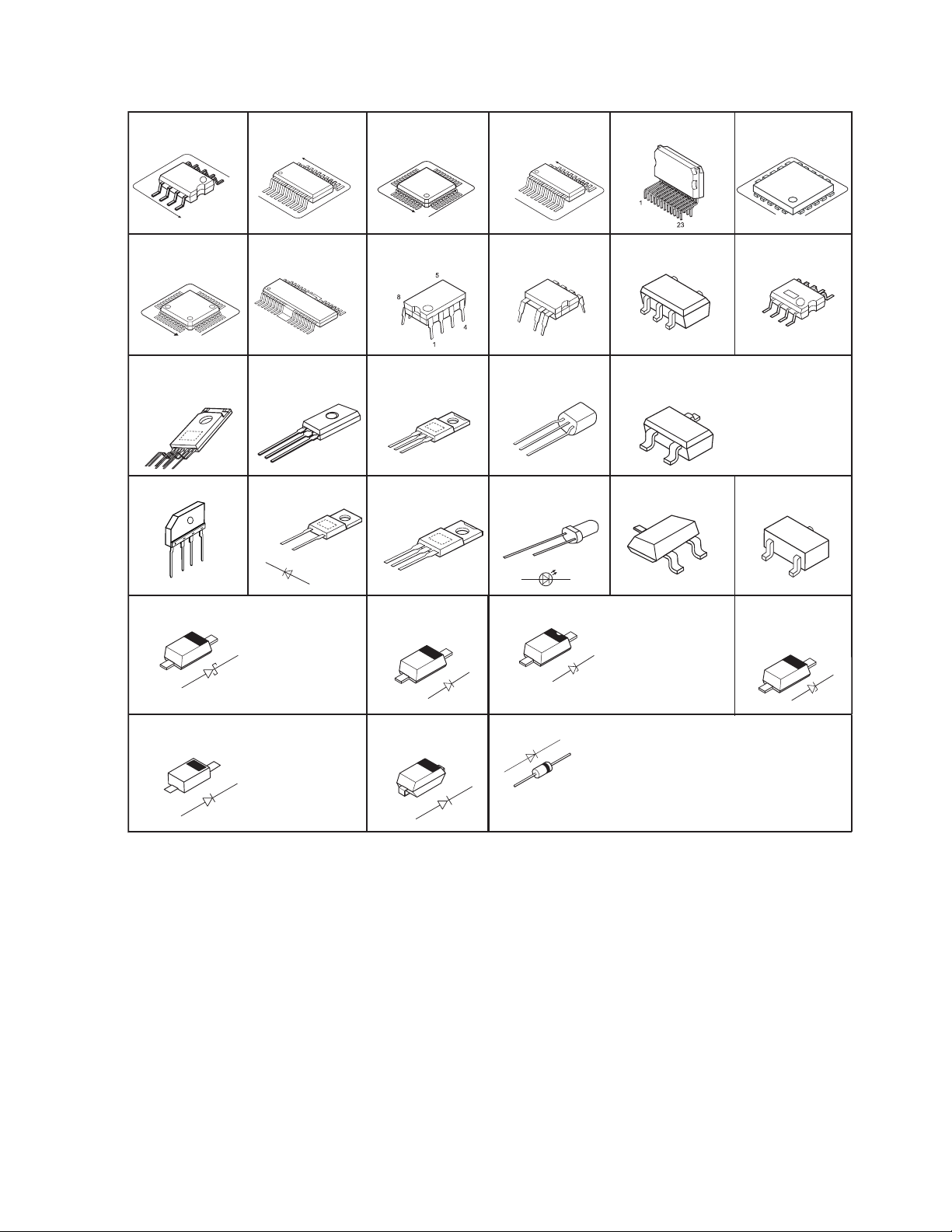
19.8. Illustration of ICs, Transistor and Diode
*Este material se encuentra sin programar, debe ser programado.
C0DBAYY01122 (8P)
No.1
No.1
C1BB00001151 (32P)C0ABBB000067 (8P)
No.1
)P32(79400000AB1C)P44(5920000ABH0C
REP4780A
(20P)
* MN101EF16KXM
(100P)
No.1
C5HACYY00004 (7P)
(PN)
C5HACYY00005 (7P)
(PH)
B0EBNR000045
-
~
~
+
Cathode
Anode
A
Cathode
Anode
A
28
1
7
29
8
B1BABG000007
E
C
B
B0HFRJ000012
B0ZAZ0000089
Cathode
Ca
DZ2J07500L
DZ2J100M0L
Ca
B0ECET000002
Ca
14
Anode
No.1
MIP2F20MSSCF (8P)C3EBEY000037 (8P)C0GBY0000117
4
3
22
30
21
15
5
7
B1BACG000048
B1BCCG000023
C0DAZYY00039
C0DAEYY00040
2
8
C0DBFYY00049 C3EBFC000042
5
1
1
2
4
3
B1ABGC000005
B1ADCE000012
B1ADCF000001
C
B
C
E
B0ABSM000008
1
2
3
B3AFA0000131
B
E
B0ADDJ000032
No.1
5
4
1
B1ABCF000176
B1ABDF000026
B1GBCFJJ0051
B1GBCFJN0033
B1GBCFLL0037
B1GDCFGA0018
B1GDCFJJ0047
B1GBCFJN0038
8
B1ABCF000231
C
Cathode
Cathode
Anode
Cathode
A
Ca
B0BC010A0007 (PH)
B0BC01700015 (PN)
Cathode
B0BC019A0007
B0BC035A0007
Ca
Ca
Anode
A
Ca
Cathod
A
Ca
Anode
B0BC6R100010
B0BC9R000008
B0EAKM000117
e
B0EAMM000057
B0HAMP000094 (PH)
A
Ca
A
A
B0ACCK000012DZ2J033M0L
DA2J10100L
Anode
A
B0ECKM000008
Anode
A
E
B
A
B0BC5R6A0266
Anode
CA
A
Cathode
Ca
A
95
Page 96
19.9. Terminal Function of ICs
19.9.1. IC2003 (*MN101EF16KXW): IC
MICRO-PROCESSOR
* Este material no se encuentra programado, se debe programar.
Pin
No.
4 OCD_SDA I/O OCD Serial data
6 OCD_SCK I/O OC Serial Clock
7 PCONT O Power Control
9 REGION_CS O Region chip select
11 MM0D0 (GND) - Ground
12 OSC2(OUT) O Oscillator Output
13 OSC1(IN) I Oscillator Input
20 ASP_CLK O ASP Clock
21 ASP_DATA I/O ASP data
22 DC_DET_AMP I DC Detect (D-AMP IC Failure
23 DC_DET_PWR I DC DETECT (Power Supply
24 BASS_SHIFT O Bass Level Meter Adjustment
28 DIMMER O LCD Display Brightness
29 CD_S_REQ I CD status request
30 BASS_SHIFT - No Connection
31 LCD_DATA O LCD data output
32 LCD_CE O LCD chip enable
33 LCD_WR O LCD write
36 CD_SCLK O CD Serial Clock
38 CD_INNER_SW I/O CD Inner switch detection
42 CD_M_REQ O CD Mode Request
43 CD_CLOSE_SW I CD Close Switch Detection
44 CD_RESET I/O CD Reset
46 CD_USB IN I CD USB Input
48 CD_OPEN_SW I CD Open Switch Detection
5
65
Terminal Name I/O Function
N01
+-8.1DDV81
Detection)
Failure Detection)
CN72
noitcennoCoN-CN1
noitcennoCoN-CN2
noitcennoCoN-CN3
noitcennoCoN-CN5
noitcennoCoN-CN8
noitcennoCoN-C
dnuorG-SSV41
tupnIrotallicsOIIX51
tuptuOrotallicsOOOX61
ylppuSegatloV3.3+-3.3DDV71
ylppuSegatloV8.1
)LevitcA(tupnIteseRITSRN91
noitcennoCoN-CN52
tupnInoitceteDeruliaFCAICNYS62
noitcennoCoN-
tupniatadlaireSDCOIS_DC43
tuptuoatadlaireSDCIOS_DC53
ylppusegatloVV8.1+-81DDV73
dnuorG-SSV93
noi
tcennoCoN-CN04
noitcennoCoN-CN14
noitcennoCoN-CN54
noitcennoCoN-CN74
noitcennoCoN-CN94
noitcennoCoN-CN0
noitcennoCoN-CN15
noitcennoCoN-CN25
noitcennoCoN-CN35
noitcennoCoN-CN45
noitcennoCoN-CN55
noitcennoCoN-CN
noitcennoCoN-CN75
Pin
No.
58 NC - No Connection
59 EE_CS O EEPROM IC Chip select
60 EE_SCL O EEPROM IC Serial clock
61 EE_SDA I/O EEPROM IC Serial data
62 CRTIMER I/O CR Timer
63 VSS - Ground
64 NC - No Connection
65 LD_CW O Loading Motor Turning Clock-
66 LD_CCW O Loading Motor Turning
67 NC - No Connection
68 MODE_DA O Digital Amp On/Off control.
69 NC - No Connection
70 NC - No Connection
71 NC - No Connection
72 NC - No Connection
73 FHOP O Frequency Hop control
74 SMPS_BP O SMPS Breatproof
75 MUTE_F O Digital Amp Muting control
76 NC - No Connection
77 NC - No Connection
78 DC-DC ENABLE O DC-DC Converter
79 TU_SDA I/O Tuner serial data
80 TU_RST O Tuner reset
81 TU_SCLK O Tuner serial clock
82 NC - No Connection
83 NC - No Connection
84 NC - No Connection
85 RMT I Remote control serial data
86 NC - No Connection
87 TU_INT I Tuner Interrupt request
88 CLIP ATTN O Clipping attenuation
89 VDD - Voltage supply
90 NC - No Connection
91 VSS - Ground
92 KEY1 I Key 1 Input
93 KEY2 I Key 2 Input
94 CLIP SENSOR I Clipping sensor (Volume &
95 AUTO BASS I Auto Bass setting adjustment
96 ROTARY JOG I Rotary jog for browse opera-
97 REGION_AD I Region setting
98 VOL_JOG I Volume Level Adjustment
99 SMPS_ID I/O SMPS Type Detection
100 VREF+ - Voltage Supply
Terminal Name I/O Function
wise (Tray Open)
Counter-Clockwise (Tray
Close)
ASP Bass control)
tion (Album & Track)
96
Page 97
19.9.2. IC900(C0HBA0000295): IC FL
Driver
Pin
No.
1 /CS I Chip Selection Input
2 /RD I Read Clock Input
3 /WR I Write Clock Input
4 DATA I/O Serial Data Input
5 VSS I Negative Power Supply
6 VLCD I LCD Power Input
7 VDD I Positive Power Supply
8 BZ O Tone Frequency Output Pair
9 COM0 O Common Output 0
10 COM1 O Common Output 1
11 COM2 O Common Output 2
12 COM3 O Common Output 3
13 SEG31 O Segment Output 31
14 SEG30 O Segment Output 30
15 SEG29 O Segment Output 29
16 SEG28 O Segment Output 28
17 SEG27 O Segment Output 27
18 SEG26 O Segment Output 26
19 SEG25 O Segment Output 25
20 SEG24 O Segment Output 24
21 SEG23 O Segment Output 23
22 SEG22 O Segment Output 22
23 SEG21 O Segment Output 21
24 SEG20 O Segment Output 20
25 SEG19 O Segment Output 19
26 SEG18 O Segment Output 18
27 SEG17 O Segment Output 17
28 SEG16 O Segment Output 16
29 SEG15 O Segment Output 15
30 SEG14 O Segment Output 14
31 SEG13 O Segment Output 13
32 SEG12 O Segment Output 12
33 SEG11 O Segment Output 11
34 SEG10 O Segment Output 10
35 SEG9 O Segment Output 9
36 SEG8 O Segment Output 8
37 SEG7 O Segment Output 7
38 SEG6 O Segment Output 6
39 SEG5 O Segment Output 5
40 SEG4 O Segment Output 4
41 SEG3 O Segment Output 3
42 SEG2 O Segment Output 2
43 SEG1 O Segment Output 1
44 SEG0 O Segment Output 0
Terminal Name I/O Function
97
Page 98
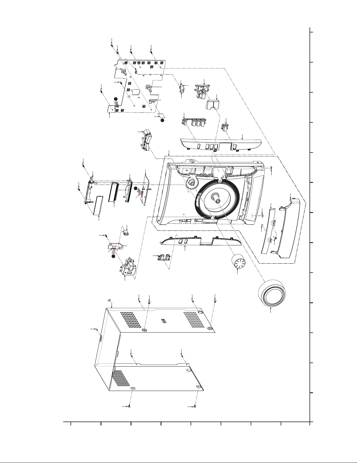
12
12
12
12
CN6005
VR6002
12
12
b
*ZJ6002
(PANEL P.C.B.)
12
25
12
Z900
28
12
39
24
b
7
CN6000
JK 1111
(LCD P.C.B.)
CN6001
3
c
VR6001
18
CN6006
IR6000
36
(REMOTE SENSOR P.C.B.)
37
34
38
32
18-3
18-2
18-3
18-1
18-4
SA-AKX14
CABINET DRAWINGS
10 11 12 13
9
8
7
98
(USB P.C.B.)
a
*ZJ6001
33
20
15
15
35
15
13
31
11
15
15
13
18-5
6
5
10
4
3
2
13
13
1
NOTE: " * " PART IS NOT SUPPLIED / REF IS FOR INDICATION ONLY.
20 Exploded View and Replacement Parts List
20.1. Exploded View and Mechanical replacement Part List
20.1.1. Cabinet Parts Location
H
G
F
E
D
C
B
A
Page 99
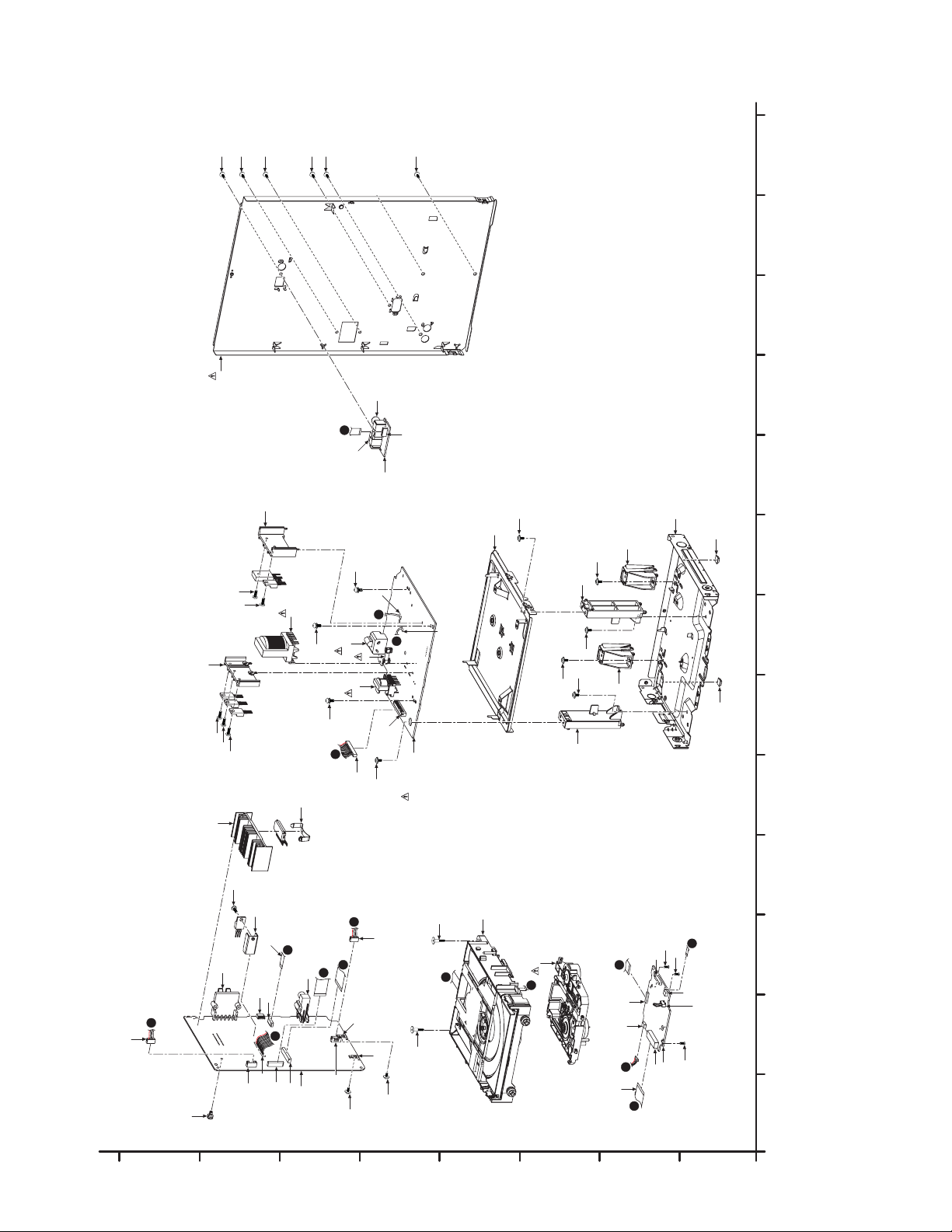
151515
21
15
15
15
JK51
15
SA-AKX14
CABINET DRAWINGS
10 11 12 13
*HEATSINK UNIT C
29
*D-AMP HEATSINK UNIT
e
JK52
*HEATSINK UNITA
17
29
29
29
29
29
T5701
17
P5701
T5751
17
f
6
23
CN51
9
(TUNER P.C.B.)
*TL7
j
*TL8
k
F1
CN5802
14
(SMPS P.C.B.)
14
42
14
22
14
14
14
26
22
41
26
19
8
99
7
19
6
5
4
*SMALL
HEATSINK
UNIT
1
e
JK5000
CN2002
CN2010
a
4
27
H
G
CN2005
CN2000
f
CN2003
CN2706
(MAIN P.C.B.)
JK2000
d
5
g
c
ZJ2000
16
ZJ2001
CN2001
F
14
14
E
(BRS1C)
16
i
310
310
h
D
301
i
C
h
CN7901
d
2
CN7001
g
*CN7801
CN7003
S7201
310
CN7002
(CD SERVO P.C.B.)
B
3
2
" ^ " PART IS FOR PH ONLY.
1
NOTE: " * " PART IS NOT SUPPLIED / REF IS FOR INDICATION ONLY.
A
Page 100
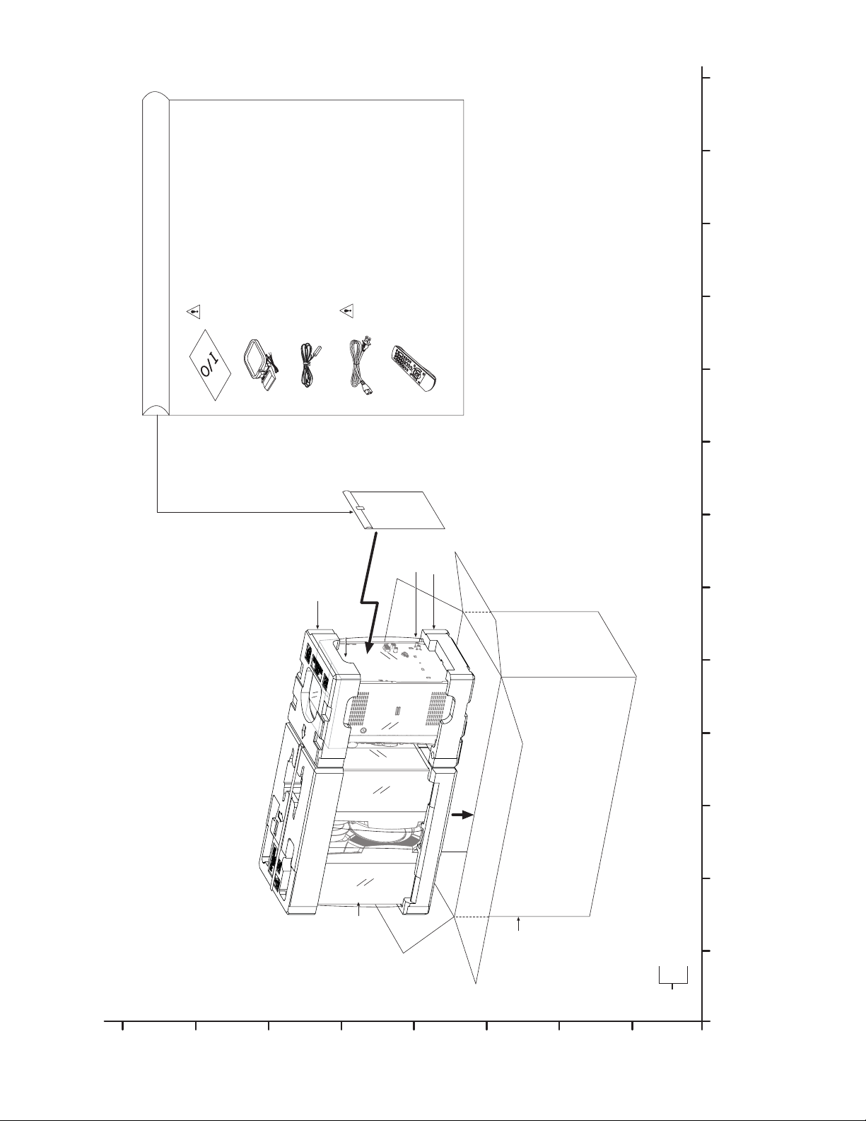
SC-AKX14
PACKAGING DRAWINGS
A3 OI BOOK
ACCESSORIES BAG
RQTM0187
AM LOOP ANTENNAA4
FM INDOOR ANTENNAA5
N1DYYYY00011
RSAX0002
*P2
SA-AKX14
A2 AC CORD
K2CB2YY00059
A1 REMOTE CONTROL
N2QAYB000636
A1-1 BATTERIES
P3
*P2
UM-3UHS/864
10 11 12 13
9
8
7
100
6
20.1.2. Packaging
5
4
FRONT
3
2
P1
POLYFOAM (TOP) RPNM0240T
POLYFOAM (BOTTOM) RPNM0240B
SB-AKX14
1
*P2
H
G
F
E
D
C
B
A
 Loading...