

Page 1

ORDER NO. MKE0503601C1
TV/DVD Combination
PV-20DF25
PV-27DF25
PV-27DF5
PV-20DF25-K
PV-27DF25-K
B6, B22
© 2005 Matsushita Kotobuki Electronics Industries
LTD. All rights reserved. Unauthorized copying and
distribution is a violation of law.
Page 2
PV-20DF25 / PV-27DF25 / PV-27DF5 / PV-20DF25-K / PV-27DF25-K
CONTENTS
Page Page
1 SAFETY PRECAUTIONS 3
1.1. GENERAL GUIDELINES
1.2. LEAKAGE CURRENT COLD CHECK
1.3. LEAKAGE CURRENT HOT CHECK
2 X-RADIATION
2.1. HORIZONTAL OSCILLATOR DISABLE CIRCUIT TEST
2.2. REPAIR PROCEDURES OF HORIZONTAL OSCILLATOR
DISABLE CIRCUIT
2.3. CIRCUIT EXPLANATION
2.4. LASER PRODUCT
2.5. PRECAUTION OF LASER DIODE
3 PREVENTION OF ELECTROSTATIC DISCHARGE (ESD) TO
ELECTROSTATICALLY SENSITIVE (ES) DEVICES
4 ABOUT LEAD FREE SOLDER (PbF)
5 SERVICE NOTES (PLEASE READ)
5.1. SERVICE NOTES
6 DISASSEMBLY/ASSEMBLY PROCEDURES
6.1. CABINET SECTION
7 ADJUSTMENT PROCEDURES
7.1. SERVICE FIXTURES AND TOOLS
7.2. ELECTRICAL ADJUSTMENT
7.3. TEST POINTS AND CONTROL LOCATION
8 SCHEMATIC DIAGRAMS
8.1. SCHEMATIC DIAGRAM AND CIRCUIT BOARD LAYOUT
NOTES
15
15
21
21
22
29
31
31
3
3
3
4
4
4
4
5
5
6
7
8
8
8.2. MAIN SCHEMATIC DIAGRAMS
8.3. DEFLECTION SCHEMATIC DIAGRAMS
8.4. OPERATION / CRT (Models : PV-20DF25 / PV-20DF25K) SCHEMATIC DIAGRAMS
8.5. CRT SCHEMATIC DIAGRAM (Models : PV-27DF25 / PV27DF25-K / PV-27DF5)
8.6. DVD MAIN / DVD SUB SCHEMATIC DIAGRAMS
8.7. INTERCONNECTION SCHEMATIC DIAGRAM
8.8. VOLTAGE CHART
9 CIRCUIT BOARD LAYOUT
9.1. MAIN C.B.A.
9.2. OPERATION C.B.A.
9.3. DEFLECTION / CRT C.B.A.
9.4. DVD MAIN / DVD SUB C.B.A.
10 B LOCK DIAGRAMS
11 EXPLODED VIEWS
11.1. DVD SECTION
11.2. CHASSIS FRAME SECTION (1)
11.3. CHASSIS FRAME SECTION (2)
11.4. CHASSIS FRAME SECTION (3)
11.5. PACKING PARTS AND ACCESSORIES SECTION
12 REPLACEMENT PARTS LISTS
12.1. REPLACEMENT NOTES
12.2. MECHANICAL REPLACEMENT PARTS LIST
12.3. ELECTRICAL REPLACEMENT PARTS LIST
32
39
40
41
42
47
48
51
51
52
53
54
55
67
67
68
69
70
71
72
72
73
74
2
Page 3

1 SAFETY PRECAUTIONS
1.1. GENERAL GUIDELINES
1. IMPORTANT SAFETY NOTICE
There are special components used in this equipment
which are important for safety. These parts are marked by
in the Schematic Diagrams, Circuit Board Layout,
Exploded Views and Replacement Parts List. It is essential
that these critical parts should be replaced with
manufacturer’s specified parts to prevent X-RADIATION,
shock, fire, or other hazards. Do not modify the original
design without permission of manufacturer.
2. An Isolation Transformer should always be used during the
servicing of Combination TV/DVD whose chassis is not
isolated from the AC power line. Use a transformer of
adequate power rating as this protects the technician from
accidents resulting in personal injury from electrical shocks.
It will also protect Combination TV/DVD from being
damaged by accidental shorting that may occur during
servicing.
3. When servicing, observe the original lead dress, especially
the lead dress in the high voltage circuits. If a short circuit is
found, replace all parts which have been overheated or
damaged by the short circuit.
4. After servicing, see to it that all the protective devices such
as insulation barriers, insulation papers, shield, and
isolation R-C combinations are properly installed.
5. Before turning the receiver on, measure the resistance
between B+ line and chassis ground. Connect (-) side of an
ohmmeter to the B+ lines, and (+) side to chassis ground.
Each line should have more resistance than specified, as
follows :
B+ Line Minimum Resistance
130 V 110 Ω (Cold chassis ground)
28 V 180 Ω (Cold chassis ground)
220 V 1 kΩ (Cold chassis ground)
6. When the TV set is not used for a long period of time,
unplug the power cord from the AC outlet.
7. Potentials, as high as 33.0 kV is present when this TV set
is in operation. Operation of the TV set without the rear
cover involves the danger of a shock hazard from the TV
set power supply. Servicing should not be attempted by
anyone who is not thoroughly familiar with the precautions
necessary when working on high voltage equipment.
Always discharge the anode of the picture tube to the CRT
ground of receiver before handling the tube.
8. After servicing make the following leakage current checks to
prevent the customer from being exposed to shock
hazards.
PV-20DF25 / PV-27DF25 / PV-27DF5 / PV-20DF25-K / PV-27DF25-K
1.2. LEAKAGE CURRENT COLD
CHECK
1. Unplug the AC cord and connect a jumper between the two
prongs on the plug.
2. For physically operated power switches, turn power on.
Otherwise skip step 2.
3. Measure the resistance value, with an ohmmeter, between
the jumpered AC plug and each exposed metallic cabinet
part on the receiver, such as screwheads, connectors, etc.
When the exposed metallic part has a return path to the
chassis, the reading should be between 1 MΩ and 12 MΩ.
When the exposed metal does not have a return path to the
chassis, the reading must be infinity.
1.3. LEAKAGE CURRENT HOT
CHECK
1. Plug the AC cord directly into the AC outlet.
Do not use a isolation transformer for this check.
2. Connect a 1.5 kΩ, 10 W resistor, in parallel with a 0.15 µF
capacitor, between each exposed metallic part on the set
and a good earth ground, as shown in Figure 1.
3. Use an AC voltmeter, with 1 kΩ/V or more sensitivity, to
measure the potential across the resistor.
4. Check each exposed metallic part, and measure the
voltage at each point.
5. Reverse the AC plug in the AC outlet and repeat each of the
above measurements.
6. The potential at any point should not exceed 0.75 V RMS.
A leakage current tester (Simpson Model 229 equivalent)
may be used to make the hot checks. Leakage current must
not exceed 1/2 mA. In case a measurement is outside of
the limits specified, there is a possibility of shock hazard,
and the receiver should be repaired and rechecked before
it is returned to the custom er.
Figure 1
3
Page 4

PV-20DF25 / PV-27DF25 / PV-27DF5 / PV-20DF25-K / PV-27DF25-K
2 X-RADIATION
WARNING :
1. The potential source of X-Radiation in TV sets is the High
Voltage section and the picture tube.
2. When using a picture tube test fixture for service, ensure
that the fixture is capable of handling 33.0 kV without
causing X-Radiation.
NOTE:
It is important to use an accurate periodically calibrated high
voltage meter.
1. Reduce the brightness to minimum.
2. Set the SERVICE switch to SERVICE.
3. Measure the High Voltage. The meter reading should
indicate 28.0 kV±1.5 kV (For model with 20 inch CRT), 31.0
kV±2.0 kV (For model with 27 inch CRT).
If the meter indication is out of tolerance, immediate service
and correction is required to prevent the possibility of
premature component failure.
4. To prevent an X-Radiation possibly, it is essential to use the
specified picture tube.
2.1. HORIZONTAL OSCILLATOR
DISABLE CIRCUIT TEST
SERVICE WARNING :
The test must be made as a final check before set is returned
to the customer.
2.2. REPAIR PROCEDURES OF
HORIZONTAL OSCILLATOR
DISABLE CIRCUIT
1. Connect a DC voltmeter between capacitor C513 (+) on the
Main circuit board and chassis ground.
2. If approximately +21.5 V (For model with 20 inch CRT),
+20.0 V (For model with 27 inch CRT) is not present at that
point when 120 V AC is applied, find the cause. Check
R508, R503, R5504, D5505, D503, C513 and C5507.
3. Carefully check above specified parts and related circuits
and parts. When the circuit is repaired, try the horizontal
oscillator disable circuit test again.
2.3. CIRCUIT EXPLANATION
2.3.1. HORIZONTAL OSCILLATOR
DISABLE CIRCUIT
The positive DC voltage, supplied from the D503 cathode for
monitoring high voltage, is applied to the IC5301 Pin 11 through
R508, R503 and R5504. Under normal conditions, the voltage
at IC5301 Pin 11 is less than approx. 6 V. If the high voltage at
Flyback Transformer Pin 5 exceeds the specified voltage, the
positive DC voltage which is supplied from the D503 cathode
also increases. The increased voltage is applied to IC5301 Pin
11 through R508, R503 and R5504. Due to the increased
voltage at IC5301 Pin 11, the horizontal oscillator frequency
increases, the picture goes out of horizontal sync, the beam
current decreases and the picture become dark in order to
keep X-radiation under specification.
CONFIRMATION OF X-RAY MOVEMENT
1. Turn off TV set.
2. Connect the circuit below between TP554 and TP553 on
the Deflection C.B.A.
Figure 2
3. Turn on SW1 and then turn on the set. Confirm that the
picture is on the screen properly.
4. Confirm that the picture goes out of horizontal sync while
getting down by varying VR.
5. If this does not occur, it means that X-ray protect circuit is
not operating. Further confirmation and repair is required.
Figure 3
4
Page 5

2.4. LASER PRODUCT
CLASS I LASER PRODUCT
· This equipment is certified to comply with DHHS Rules 21
CFR Chapter 1, Subchapter J in effect as of date of
manufacture. (Only for U.S.A.)
This equipment is classified as a Class I (Class 1) level LASER
Product and there is no hazardous LASER radiation with the
safety protection.
Caution:
Use of controls or adjustments or performance of
procedures other than those specified herein may result in
hazardous radiation exposure.
Never touch the internal parts in order to avoid EXPOSURE TO
VISIBLE LASER RADIATION.
Unplug the AC power cord to the equipment when opening the
top cover.
PV-20DF25 / PV-27DF25 / PV-27DF5 / PV-20DF25-K / PV-27DF25-K
When the power switch is On, do not place your eyes close to
the front panel opening door or the other openings to look into
the interior unit.
LASER Specification
Class I level A LASER Product (Class 1 level A LASER
Product)
Wave Length: 640 - 677 nm (at DVD)
770 - 810 nm (at CD)
Laser Power: No hazardous radiation is emitted with
the safety protection.
2.5. PRECAUTION OF LASER
DIODE
CAUTION:
This unit utilizes a class III a laser. Visible laser radiation is
emitted from the optical pickup lens when the unit is turned
on:
1. Do not look directly into the pickup lens.
2. Do not use optical instruments to look at the pickup lens.
3. Do not adjust the preset variable resistor on the optical
pickup.
4. Do not disassemble the optical pickup unit.
5. If the optical pickup is replaced, use the manufactures
specified replacement pickup only.
6. Use of control or adjustment or performance of procedures
other than those specified herein may result in hazardous
radiation exposure.
5
Page 6

PV-20DF25 / PV-27DF25 / PV-27DF5 / PV-20DF25-K / PV-27DF25-K
3 PREVENTION OF ELECTROSTATIC DISCHARGE (ESD)
TO ELECTROSTATICALLY SENSITIVE (ES) DEVICES
Some semiconductor (solid state) devices can be damaged easily by static electricity. Such components commonly are called
Electrostatically Sensitive (ES) Devices. Examples of typical ES devices are integrated circuits and some field-effect transistors are
semiconductor "chip" components. The following techniques should be used to help reduce the incidence of component damage
caused by electrostatic discharge (ESD).
1. Immediately before handling any semiconductor component or semiconductor-equipped assembly, drain off any ESD on your
body touching a known earth ground. Alternatively, obtain and wear a commercially available discharging ESD wrist strap, which
should be removed for potential shock reasons prior to applying power to the unit under test.
2. After removing an electrical assembly equipped with ES devices, place the assembly on a conductive surface such as
aluminum foil, to prevent electrostatic charge buildup or exposure of the assembly.
3. Use only a grounded-tip soldering iron to solder or unsolder ES devices.
4. Use only an anti-static solder removal device. Some solder removal devices not classified as "anti-static (ESD protected)" can
generate electrical charge sufficient to damage ES devices.
5. Do not use freon-propelled chemicals. These can generate electrical charges sufficient to damage ES devices.
6. Do not remove a replacement ES device from its protective package until immediately before you are ready to install it. (Most
replacement ES devices are packaged with leads electrically shorted together by conductive foam, aluminum foil or comparable
conductive material).
7. Immediately before removing the protective material from the leads of a replacement ES device, touch the protective material
to the chassis or circuit assembly into which the device will be installed.
CAUTION:
Be sure no power is applied to the chassis or circuit, and observe all other safety precautions.
8. Minimize bodily motions when handling unpackaged replacement ES devices. (Otherwise harmless motion such as the
brushing together of your clothes fabric or the lifting of your foot from a carpeted floor can generate static electricity (ESD)
sufficient to damage an ES device).
"NOTEtoCATVsysteminstaller:
This reminder is provided to call the CATV system installer’s attention to Article 820-40 of the NEC that provides guidelines for
proper grounding and, in particular, specifies that the cable ground shall be connected to the grounding system of the building,
as close to the point of cable entry as practical."
6
Page 7

4 ABOUT LEAD FREE SOLDER (PbF)
PV-20DF25 / PV-27DF25 / PV-27DF5 / PV-20DF25-K / PV-27DF25-K
7
Page 8
PV-20DF25 / PV-27DF25 / PV-27DF5 / PV-20DF25-K / PV-27DF25-K
5 SERVICE NOTES (PLEASE READ)
5.1. SERVICE NOTES
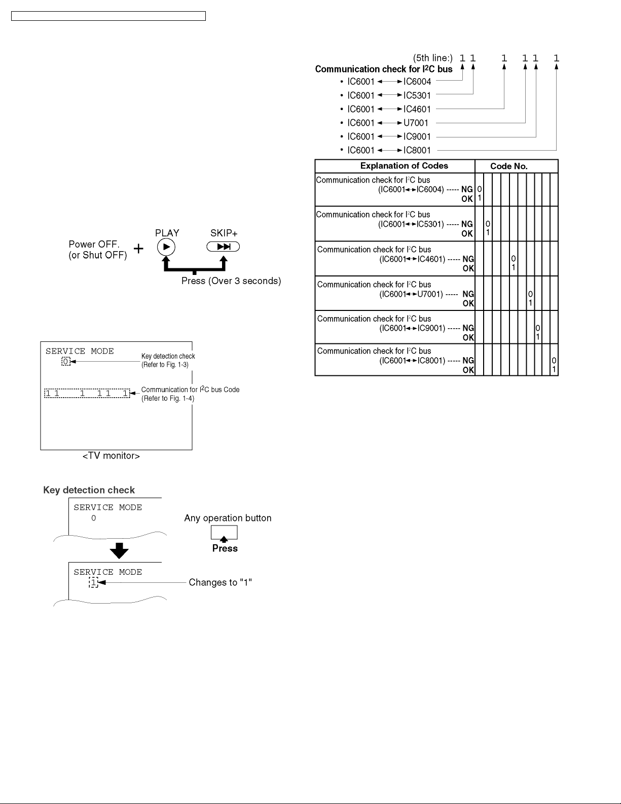
5.1.1. SIMPLIFIED FAULT FINDING DATA
Simplified Self-Diagnostic System facilitates finding the cause
of the fault. The Communication for I
displayed on the TV screen.
The Simplified Fault finding data is stored in the Memory IC
(IC6004). This data is cleared after it is displayed, and then the
POWER button is pressed back on.
1. With power turned off, press PLAY and SKIP+ buttons on
the unit together for over 3 seconds.
Fig. 1-1
2. TV power comes on and the unit goes into service mode.
The Communication for I
2
C bus code will be displayed.
2
C bus code will be
Fig. 1-4
Fig. 1-2
Fig. 1-3
Note:
Press any operation button except for POWER or PLAY
buttons on either the unit, or DVD key on the remote to
detect that a key has been pressed. The 3rd digit
changes to "1" only when key is detected.
8
Page 9

5.1.2. USAGE SCREEN MODE
This function is displayed on the TV monitor:
· the total AC plugged in AC socket (in days)
· the total elapsed "DVD play" time (in hours).
1. With power turned, press STOP button on the unit and 7
key on the remote together.
The USAGE SCREEN will be displayed on the TV Monitor.
Fig. 2
Note:
1. After replacing the DVD Unit, press ADD/DLT button on
remote in this mode. Only Total elapsed time "DVD Play"
time (in hours) will be cleared to 0.
2. To release from Usage Screen Mode, press any operation
button or insert a cassette tape in this mode. The unit will
return to normal operation mode.
PV-20DF25 / PV-27DF25 / PV-27DF5 / PV-20DF25-K / PV-27DF25-K
5.1.4. METHOD FOR EJECTING THE DVD
TRAY MANUALLY
1. Insert a Screwdriver or similar object into the Eject hole.
2. Press it gently, and then pull the Tray fully out.
Fig. 4
5.1.3. GROUNDING FOR
ELECTROSTATIC BREAKDOWN
Prevention
1. Human body grounding
Use the antistatic wrist strap to discharge the static
electricity from your body.
2. Work table grounding
Put a conductive material (sheet) or steel sheet on the area
where the optical pickup is placed and ground the sheet.
Caution:
The static electricity of your clothes will not be grounded
through the wrist strap. So take care not to let your clothes
touch the optical pickup.
Fig. 3
9
Page 10

PV-20DF25 / PV-27DF25 / PV-27DF5 / PV-20DF25-K / PV-27DF25-K
5.1.5. DVD SERVICE MODE
This unit has a Self-Diagnostic function which detects a
problem or malfunction within the unit and displays it on the TV
screen.
5.1.5.1. How to enter DVD Service Mode
1. Set the unit to DVD mode.
2. Press and hold the STOP, SKIP+, and VOL- buttons on the
unit together for over 5 seconds. The adjustment overlay
will appear on the TV screen.
Fig. 5-1
3. Press the DISPLAY key on the remote control to enter DVD
Service Mode I.
defective by checking the value of JITTER and the value of
LASER (current).
Fig. 5-2
4. Press the LEFT or RIGHT key on the remote again to enter
DVD Service Mode II.
Fig. 5-3
Note:
a. After replacing the DVD Unit, press the CLEAR key
on the remote in this mode. The total elapsed "Disc
Motor on" time (in hours/minutes) will be cleared to
0.
b. If 01 or 02 is always displayed in 9 DM STATUS,
replace the DVD Unit because the Disc Motor is
defective.
5. To confirm the value of JITTER and the value of LASER
(current), insert the DVD Test Disc into the DVD Unit.
6. To release from this mode, turn off the power.
5.1.5.2. Troubleshooting hint (standard)
for this mode
It can be determine whether the DVD Mechanism Unit is
10
Page 11

5.1.6. SERVICE POSITION
CAUTION:
1. HOT CIRCUIT (Primary circuit) exists on the Main
C.B.A.
Use extreme care to prevent accidental shock when
servicing.
2. Before connecting the AC plug, be sure to confirm the
connection between the Connector P502 on the
Deflection C.B.A. and P851/P852 on the Main C.B.A.
Otherwise, some electrical parts may be damaged due
to a sudden power surge.
PV-20DF25 / PV-27DF25 / PV-27DF5 / PV-20DF25-K / PV-27DF25-K
5.1.6.1.2. Service Position (2)
1. Remove the Rear Cover. Then, turn the DVD Ass´y to the
right.
2. Connect the DVD Main C.B.A. using the Extension Cable
16P.
5.1.6.1. How to obtain Service Position
for Combination TV/DVD models
To obtain these Service Positions, the 2 Extension Cables 13P
(LSUA0047) and 16P (LSUA0048) are necessary.
5.1.6.1.1. Service Position (1)
1. Remove the Rear Cover. Then, pull the DVD Ass´y out and
place it upright.
Fig. 6-2
5.1.6.1.3. Service Position (3)
1. Remove the Rear Cover. Then, pull out the DVD Ass´y.
2. Place the Deflection C.B.A. and the Main C.B.A. upright.
Then, connect them using the Extension Cable 13P.
Fig. 6-1
Fig. 6-3
11
Page 12
PV-20DF25 / PV-27DF25 / PV-27DF5 / PV-20DF25-K / PV-27DF25-K
5.1.7. HOT CIRCUIT
Primary circuit exists on the Main C.B.A.
This circuit is identified as " HOT " on the C.B.A. and in the
Service Manual. Use extreme care to prevent accidental shock
when servicing.
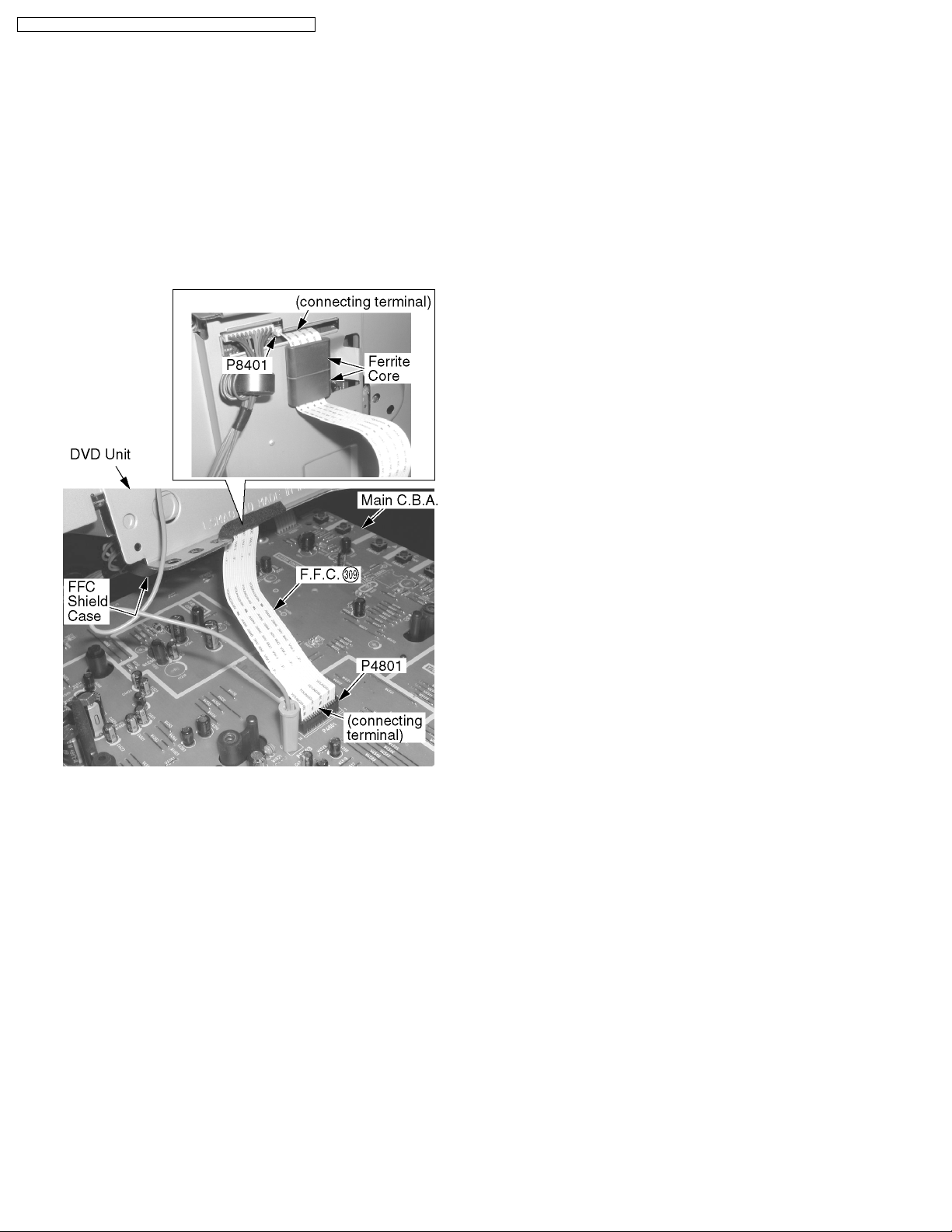
5.1.8. F.F.C. CONNECTION NOTE
5.1.8.1. F.F.C. between the DVD Unit
(DVD Main C.B.A.) and the Main
C.B.A.
Be careful with the direction of F.F.C. to connector as shown.
Fig. 7
12
Page 13

5.1.9. WIRE AND LEAD POSITION DIAGRAM
PV-20DF25 / PV-27DF25 / PV-27DF5 / PV-20DF25-K / PV-27DF25-K
Fig. 8
13
Page 14

PV-20DF25 / PV-27DF25 / PV-27DF5 / PV-20DF25-K / PV-27DF25-K
5.1.10. HOW TO RESET ALL
COMBINATION TV/DVD MEMORY
FUNCTIONS
To reset (clear) the select language, channel auto set and set
clock functions to their initial power on condition, hold down the
PLAY and SKIP- buttons of operation panel on the unit together
for more than 5 seconds.
Power will shut off.
5.1.11. HOW TO CONFIRM AUTO CLOCK
SET FEATURE
1. Connect an RF cable from the output of one unit to the input
of the test unit.
2. Select corresponding RF channels.
3. Playback a recording of P.B.S. channel including clock set
data and confirm this feature.
5.1.12. VARIABLE VOLTAGE ISOLATION
TRANSFORMER
An Isolation Transformer should always be used during the
servicing of Combination TV/DVD whose chassis is not isolated
from the AC power line. Use a transformer of adequate power
rating as this protects the technician from accidents resulting in
personal injury from electrical shocks. It will also protect
Combination TV/DVD from being damaged by accidental
shorting that may occur during servicing.
Also, when troubleshooting the above type of Power Supply
Circuit, a variable isolation transformer is required in order to
increase the input voltage slowly.
5.1.13. SPECIAL NOTE
All integrated circuits and many other semiconductor devices
are electrostatically sensitive and therefore require the special
handling techniques described under the
"ELECTROSTATICALLY SENSITIVE (ES) DEVICES" section
of this service manual.
5.1.14. MODEL NO. IDENTIFICATION
MARK
Use Marks shown in the chart below to distinguish the different
models included in this Service Manual.
14
Page 15

PV-20DF25 / PV-27DF25 / PV-27DF5 / PV-20DF25-K / PV-27DF25-K
6 DISASSEMBLY/ASSEMBLY PROCEDURES
6.1. CABINET SECTION
6.1.1. Disassembly Flowchart
Perform all disassembly procedures in the order described in the "Disassembly Flowchart" shown below. When reassembling, use
the reverse procedure.
CAUTION:
1. Disconnect AC plug before disassembly.
2. Before connecting the AC plug, be sure to confirm the connection between the Connector P502 on the Deflection C.B.A.
and P851/P852 on the Main C.B.A. Otherwise, some electrical parts may be damaged due to a sudden power surge.
Fig. D1
15
Page 16

PV-20DF25 / PV-27DF25 / PV-27DF5 / PV-20DF25-K / PV-27DF25-K
Fig. D2
16
Page 17

PV-20DF25 / PV-27DF25 / PV-27DF5 / PV-20DF25-K / PV-27DF25-K
Fig. D3
17
Page 18

PV-20DF25 / PV-27DF25 / PV-27DF5 / PV-20DF25-K / PV-27DF25-K
Fig. D4
18
Page 19

6.1.1.1. Notes in chart
1. Removal of DVD Ass’y
PV-20DF25 / PV-27DF25 / PV-27DF5 / PV-20DF25-K / PV-27DF25-K
Fig. D5
2. Removal of Color Picture Tube Unit
Place the Unit face down on a soft cloth before removing the Color Picture Tube Unit.
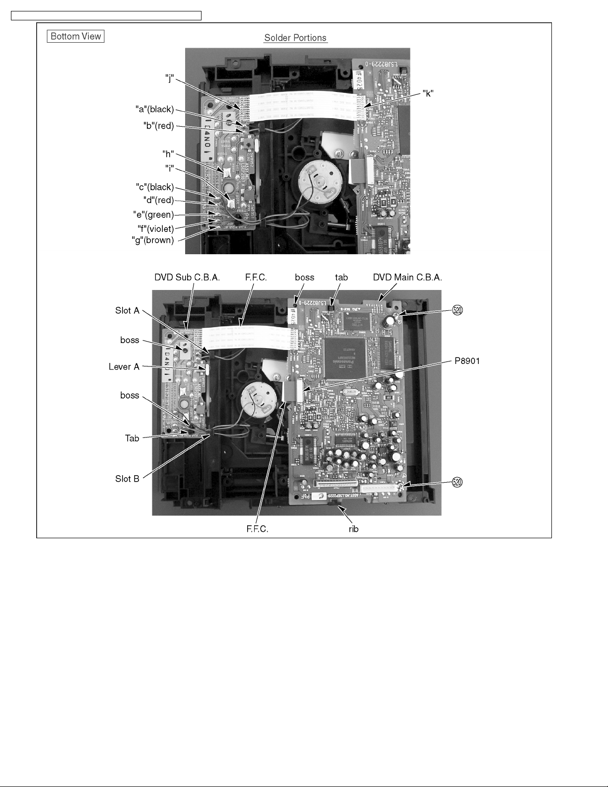
3. Removal of DVD Sub C.B.A.
a. Remove solder portions "a, b, c, d, e, f, g, h, i, j" on the DVD Sub C.B.A.
b. Remove the DVD Sub C.B.A. while releasing the Locking Tab.
Installation of DVD Main C.B.A. and DVD Sub C.B.A.
a. Confirm that the Lever A is positioned as shown, and install the DVD Sub C.B.A. with the Locking Tab and 2 bosses.
b. Install the DVD Main C.B.A. with the Locking Tab and the rib.
c. Pass the leads through the slots A and B.
d. Solder portions "a, b, c, d, e, f, g, h, i, j, k" on the C.B.A.
Note:
Solder portions "h" and "i" while pushing down the DVD Sub C.B.A. securely.
e. Connect the F.F.C.s to Connectors P8901 on the DVD Main C.B.A.
f. Tighten the 2 Screws (520).
19
Page 20
PV-20DF25 / PV-27DF25 / PV-27DF5 / PV-20DF25-K / PV-27DF25-K
Fig. D6
20
Page 21

7 ADJUSTMENT PROCEDURES
7.1. SERVICE FIXTURES AND TOOLS
PV-20DF25 / PV-27DF25 / PV-27DF5 / PV-20DF25-K / PV-27DF25-K
21
Page 22

PV-20DF25 / PV-27DF25 / PV-27DF5 / PV-20DF25-K / PV-27DF25-K
7.2. ELECTRICAL ADJUSTMENT
NOTE:
Following Adjustments have been preadjusted at factory and
are not required.
· Purity Adjustment
· Convergence Adjustment
7.2.1. TEST EQUIPMENT
To do all of these electrical adjustments, the following
equipment is required.
1. Dual-Trace Oscilloscope
Voltage Range: 0.001 V to 50 V/Div.
Frequency Range: DC to 50 MHz
Probes: 10:1, 1:1
2. NTSC Video Pattern Generator
3. Isolation Transformer (Variable)
4. Degaussing Coil
5. White Pattern Generator
7.2.3. EVR (Electronic Variable Register)
ADJUSTMENT WITH THE REMOTE
CONTROL
This unit has electronic technology using I2C Bus concept.
The following control functions are adjusted by using "On
Screen Displays" and the remote control instead of adjusting
mechanical controls (VR).
7.2.2. HOW TO READ THE ADJUSTMENT
PROCEDURES
Fig. E1
7.2.4. EVR ADJUSTMENT ITEM
The following Items need to be adjusted for EVR adjustment.
· SUB CONTRAST ADJUSTMENT
· FOCUS, SCREEN, CUT OFF, DRIVE ADJUSTMENT
· SUB COLOR/SUB TINT ADJUSTMENT
· DEFLEC TION DISTORTION CORRECTION
ADJUSTMENT
· WHITE BALANCE ADJUSTMENT
· SUB BRIGHTNESS ADJUSTMENT
7.2.5. HOW TO ENTER EVR
ADJUSTMENT MODE
Press and hold STOP, SKIP + and VOL - buttons on the unit
together over 5 seconds.
The adjustment overlay will appear to Enter EVR adjustment
mode.
Fig. E2-1
7.2.5.1. How to adjust:
1. Press UP/DOWN key on the remote control to
select control function to be adjusted.
22
Page 23

Important Note:
Make a note of the original value of the controls
before modifying in case the wrong control is
adjusted.
2. Press RIGHT/LEFT
that the shaded area moves to the value.
3. Press UP/DOWN key on the remote control to
adjust the value of the selected control.
key on the remote control so
Fig. E2-2
PV-20DF25 / PV-27DF25 / PV-27DF5 / PV-20DF25-K / PV-27DF25-K
7.2.5.3. HOW TO ENTER SERVICE MODE
1. Set the unit to TV Mode.
2. Enter EVR adjustment mode.
3. Press DISPLAY key on the remote control for collapse
scan.
Note:
Before pressing DISPLAY key on the remote control for
collapse scan, select the desired control function and move
the shaded area to the value for adjustments you will
proceed.
Fig. E2-6
Fig. E2-3
Note:
You can select a desired channel by using the
numbered keys on the remote control in EVR
adjustment mode.
4. Press RIGHT/LEFT
that the shaded area moves to the control function.
5. Press UP/DOWN key on the remote control to
select a control function for the next adjustment if
necessary.
key on the remote control so
Fig. E2-4
Fig. E2-5
7.2.5.4. How to release from Service
Mode:
Press DISPLAY key again on the remote control.
7.2.5.2. How to release from EVR
Adjustment Mode:
Press and hold STOP, SKIP + and VOL - buttons on the unit
together over 5 seconds again or press the POWER button
OFF to release EVR adjustment mode. The adjusted value will
be written to Memory IC (IC6004).
23
Page 24
PV-20DF25 / PV-27DF25 / PV-27DF5 / PV-20DF25-K / PV-27DF25-K
7.2.6. SUB CONTRAST ADJUSTMENT
Purpose: To set the optimum sub contrast level.
Symptom of
Misadjustment:
Test Point : TP49 (CRT C.B.A.)
Adjustment : SUB CONTRAST (EVR),
Specification : Refer to descriptions below.
Input : Video Input Jack,
Mode : STOP
Equipment : Oscilloscope,
1. Supply a Crosshatch Pattern Signal to the Video Input Jack.
2. Connect the Oscilloscope to TP49 on the CRT C.B.A.
(Use TP47 for GND.)
3. Select SUB BRIGHT in EVR adjustment mode. Then, after
making a note of the original value, adjust to the (C0).
4. Select SUB CONTRAST in EVR adjustment mode and
adjust so that the level A is (3.0 V[p-p]±0.1 V[p-p]: For
model with 20 inch CRT), or (3.15 V[p-p]±0.1 V[p-p]: For
model with 27 inch CRT).
5. Select SUB BRIGHT in EVR adjustment mode and reset to
the original value.
The picture is too dark or too light.
Crosshatch Pattern Signal 1 V[p-p] (75 Ω
terminated)
NTSC Video Pattern Generator
7.2.7. FOCUS, SCREEN, CUT OFF, DRIVE
ADJUSTMENT
Purpose: To set the optimum Screen.
Symptom of
Misadjustment:
Test Point : TP50 (CRT C.B.A.)
Adjustment : FOCUS CONTROL
Specification : Refer to descriptions below.
Input : Video Input Jack,
Mode : STOP
Equipment : Oscilloscope,
1. Supply a Crosshatch Pattern Signal to the Video Input Jack.
2. Adjust the FOCUS CONTROL on the Flyback Transformer
so that the "a" and "b" are the sharpest.
The picture is will be an improper screen
color mix.
(Flyback Transformer),
SCREEN CONTROL (Flyback
Transformer),
SUB BRIGHT (EVR),
G DRIVE (EVR),
B DRIVE (EVR),
R CUT-OFF (EVR),
G CUT-OFF (EVR),
B CUT-OFF (EVR)
Crosshatch Pattern Signal,
Monoscope Pattern Signal
NTSC Video Pattern Generator
Fig. E3
Fig. E4-1
3. Supply a Monoscope Pattern Signal to the Video Input
Jack.
4. Connect the Oscilloscope to TP50 on the CRT C.B.A.
(Use TP47 for GND.)
5. Select SUB BRIGHT and move the shaded area to the
value in EVR adjustment mode.
6. Turn the SCREEN CONTROL on the Flyback Transformer
fully counterclockwise.
7. Press DISPLAY key on the remote control for collapse
scan. (Refer to "HOW TO ENTER SERVICE MODE.")
8. Adjust SUB BRIGHT in EVR adjustment mode so that the
level A is (170 VDC±5 VDC: For model with 20 inch CRT),
or (185 VDC±5 VDC: For model with 27 inch CRT).
24
Page 25

Fig. E4-2
9. Turn the SCREEN CONTROL on the Flyback Transformer
clockwise carefully and stop at the point where any color is
first observed.
10. In EVR adjustment mode, select the two colors not
observed in step 8 from the following control functions (R
CUT-OFF, G CUT-OFF, B CUT-OFF) and adjust so that the
horizontal line becomes white.
For example, if the horizontal line appeared red in step 8,
select and adjust the B CUT-OFF and G CUT-OFF. (See
NOTE)
11. Press DISPLAY key on the remote control again to return
for full frame scan.
12. Select SUB BRIGHT in EVR adjustment mode and adjust
so that the picture has adequate brightness.
13. Select G DRIVE and B DRIVE in EVR adjustment mode
and adjust so that the entire screen is white.
Note:
Before pressing DISPLAY key on the remote control for
collapse scan, select the desired control function and move
the shaded area to the value.
PV-20DF25 / PV-27DF25 / PV-27DF5 / PV-20DF25-K / PV-27DF25-K
7.2.8. SUB COLOR/SUB TINT
ADJUSTMENT
Purpose : To set the standard color phase.
Symptom of
Misadjustment :
Test Point : TP49 (CRT C.B.A.)
Adjustment : SUB COLOR (EVR),
Specification : Refer to descriptions below.
Input : Video Input Jack,
Mode : STOP
Equipment : Oscilloscope,
1. Supply the Rainbow Color Bar signal to Video Input Jack.
2. Connect the Oscilloscope to TP49 on the CRT C.B.A.
3. Select SUB BRIGHT in EVR adjustment mode. Then, after
making a note of original value, adjust to the (C0).
4. Select SUB TINT in EVR adjustment mode and adjust so
that level A and B should be equal in amplitude.
Color phase will be shifted.
SUB TINT (EVR),
Rainbow Color Bar
NTSC Video Pattern Generator
Fig. E5-1
5. Select SUB COLOR in EVR adjustment mode and adjust
which higher level that level C is 1.40 V[p-p]±0.15 V[p-p].
Fig. E5-2
25
Page 26

PV-20DF25 / PV-27DF25 / PV-27DF5 / PV-20DF25-K / PV-27DF25-K
6. Select SUB TINT in EVR adjustment mode and increase
level B 1 clicks above the same level.
Fig. E5-3
7. Select SUB BRIGHT in EVR adjustment mode and reset to
the original value.
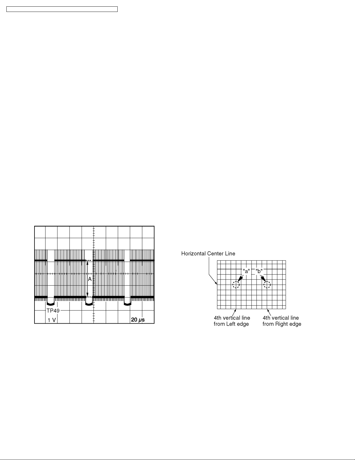
7.2.9. DEFLECTION DISTORTION
CORRECTION ADJUSTMENT
Purpose : To set the optimum picture.
Symptom of
Misadjustment :
Test Point : ---------Adjustment : V POSITION (EVR),
Specification : Refer to descriptions below.
Input : Video Input Jack,
Mode : STOP
Equipment : NTSC Video Pattern Generator
The picture is distortion.
V SIZE (EVR),
H-CENTER (EVR),
(For model with 27 inch CRT)
R763 (Deflection C.B.A.),
R753 (Deflection C.B.A.),
R766 (Deflection C.B.A.)
Crosshatch Pattern Signal,
Monoscope Pattern Signal
1. Supply a Crosshatch Pattern Signal to the Video Input Jack.
2. Confirm that the Horizontal Center Line is within the limits of
A.
Fig. E6-1
3. (For model with 27 inch CRT)
Adjust R763 so that vertical lines should be almost straight.
4. (For model with 27 inch CRT)
Adjust R753 so that vertical lines at Left edge and Right
edge should be almost straight.
5. Supply a Monoscope Pattern Signal to the Video Input
Jack.
6. Select V POSITION in EVR adjustment mode and adjust
Horizontal Center Line is within the limits of A.
26
Page 27

Fig. E6-2
7. Select V SIZE in EVR adjustment mode and adjust so that
the top 4th line is just in view, and that the Bottom edge is
between the 9th line and the 11th line.
8. Select H-CENTER in EVR adjustment menu and adjust so
that B is approximately equal to width C.
9. (For model with 27 inch CRT)
Adjust R766 so that the left 4th line is just in view.
10. Supply a Crosshatch Pattern Signal to the Video Input Jack.
Then, confirm that the picture is no distortion.
PV-20DF25 / PV-27DF25 / PV-27DF5 / PV-20DF25-K / PV-27DF25-K
7.2.10. WHITE BALANCE ADJUSTMENT
Purpose: To set the standard white level for each
color temperature.
Symptom of
Misadjustment :
Test Point : TP50 (CRT C.B.A)
Adjustment : FOCUS CONTROL
Specification : Refer to descriptions below.
Input : Video Input Jack,
Mode : STOP
Equipment : NTSC Video Pattern Generator,
1. Supply a Monoscope Pattern Signal to the Video Input
Jack.
2. Connect the Oscilloscope to TP50 on the CRT C.B.A.
(Use TP47 for GND.)
3. Select SUB BRIGHT and move the shaded area to the
value in EVR adjustment mode.
4. Adjust the FOCUS CONTROL on the Flyback Transformer
so that the "a" and "b" are the sharpest.
White becomes bluish or reddish.
(Flyback Transformer),
SCREEN CONTROL (Flyback
Transformer),
SUB BRIGHT (EVR),
G DRIVE (EVR),
B DRIVE (EVR),
R CUT-OFF (EVR),
G CUT-OFF (EVR),
B CUT-OFF (EVR)
Monoscope Pattern Signal,
White Pattern Signal
White Pattern Generator,
Oscilloscope
Fig. E7-1
5. Turn the SCREEN CONTROL on Flyback Transformer fully
counterclockwise.
6. Press DISPLAY key on the remote control for collapse
scan. (Refer to "HOW TO ENTER SERVICE MODE.")
7. Adjust SUB BRIGHT in EVR adjustment mode so that the
level A is 175 VDC±5 VDC.
27
Page 28

PV-20DF25 / PV-27DF25 / PV-27DF5 / PV-20DF25-K / PV-27DF25-K
Fig. E7-2
7.2.11. SUB BRIGHTNESS ADJUSTMENT
Note:
Perform this adjustment in a darkened room.
Purpose : To set the optimum brightness level.
Symptom of
Misadjustment :
Test Point : ---------Adjustment : SUB BRIGHT (EVR),
Specification : Refer to descriptions below.
Input : ---------Mode : STOP
The picture is too white or too black.
8. Turn the SCREEN CONTROL on the Flyback Transformer
clockwise carefully and stop at the point where red or blue
is first observed.
9. In EVR adjustment mode, select the two colors not
observed in step 8 from the following control functions (R
CUT-OFF, G CUT-OFF, B CUT-OFF) and adjust so that the
horizontal line becomes white.
For example, if the horizontal line appeared red in step 8,
select and adjust the B CUT-OFF and G CUT-OFF. (See
NOTE)
10. Supply a White Pattern Signal to the Video Input Jack.
11. Press DISPLAY key on the remote control again to return
for full frame scan.
12. Select G DRIVE and B DRIVE in EVR adjustment mode
and adjust so that the entire screen is white.
13. Confirm that the screen is tracking the White Pattern
properly. If NG, repeat the above steps 8, 9 and 12 until the
screen is properly tracking the White Pattern.
14. Select SUB BRIGHT in EVR adjustment mode and adjust
correctly.
Note:
Before pressing DISPLAY key on the remote control for
collapse scan, select the desired control function and move
the shaded area to the value.
1. Do not input any signal to the unit.
2. Set INPUT SELECT item to LINE in SET UP TV menu to
display black screen.
3. Select SUB BRIGHT in EVR adjustment mode, and adjust
so that the black screen starts to turn gray (lighting only).
28
Page 29

7.3. TEST POINTS AND CONTROL LOCATION
PV-20DF25 / PV-27DF25 / PV-27DF5 / PV-20DF25-K / PV-27DF25-K
29
Page 30

PV-20DF25 / PV-27DF25 / PV-27DF5 / PV-20DF25-K / PV-27DF25-K
30
Page 31

8 SCHEMATIC DIAGRAMS
8.1. SCHEMATIC DIAGRAM AND CIRCUIT BOARD LAYOUT NOTES
PV-20DF25 / PV-27DF25 / PV-27DF5 / PV-20DF25-K / PV-27DF25-K
1. Important safety notice
Components identified by the sign
have special
characteristics important for safety. When replacing any
of these components. Use only the specified parts.
2. Do not use the part number shown on this drawing for
ordering.
The correct part number and part value is shown in the
parts list, and may be slightly different or amended since
this drawing was prepared.
3. Use only original replacement parts:
To maintain original function and reliability of repaired
units, use only original replacement parts which are listed
with their part numbers in the parts list section of the
service manual.
4. Parts different in shape or size may be used.
However, only interchangeable parts will be supplied as
service replacement parts.
5. Test point information
:Test point with a jumper wire across a hole in P.C.B.
:Test point with a component lead on the foil side.
:Test point with no test pin.
:Test point with a test pin.
Schematic Diagram Notes
1. Indication for Zener Voltage of Zener Diodes
The Zener Voltage of Zener Diodes are indicated as such
on Schematic Diagrams.
3. Parts marked "PT" are not used in any models included
in this service model.
Example:
C6011
100P
C6011
PT
R6097
PT
PT
4. Jumper wires are used for WA10, WA5 etc and these are
not supplied as replacement parts.
Signal Waveform Note
How to read Signal Waveform
9
CH1 TP3002
CH2 TP6205
0.1V 5ms 2
1 2 3 4 5 6 7
WF1
+250mVp-pV1
REC SP/LP/SLP
5V
8
Voltage Chart Note
Voltage Measurement
a. Color bar signal in SP mode.
b. ---:Unmeasurable or not necessary to measure.
1 Connecting Point
2 Volts/Div
3 Volts/Div
4 Connecting Point
5 Time/Div
6 Trigger Channel of
the scope
(1:CH1,2:CH2)
7 Operation Mode of
VCR
8 Waveform Point on
Schematic
9 V1:Peak to Peak
Example:
(6.2V)......Zener Voltage
2. How to identify Connectors
Each connector is labeled with a Connector No. and Pin
No. Indicating what it is connected to,
in other words, its counter part.
Use the interconnection schematic diagram to find the
connection between associated connectors.
Example:
The connections between C.B.A.s are shown below.
Ref. No. of the connection parts such as lead cable,
flexible cable which is supplied as a replacement parts.
The Number of pins of the Connector.
POWER SUPPLY
C.B.A.
P1503
244
(10 Pins)
MAIN C.B.A.
P3004
Connector No.
on Main C.B.A.
Circuit Board Layout Note
Circuit Board Layout shows components installed for
various models.
For proper parts content for the model you are servicing,
please refer to the schematic diagram and parts list.
NOTE:
Circuit Board Layout includes components which are not
used.
Model No. Identification Mark
MODEL
PV-20DF25
PV-20DF25-K
PV-27DF25
PV-27DF25-K
PV-27DF5
Not Used
Note : Refer to item 3 of Schematic Diagram Notes for mark "PT".
SCHEMATIC DIAGRAM & CIRCUIT BOAD LAYOUT NOTES
PV-20DF25/PV-20DF25-K/PV-27DF25/PV-27DF25-K/PV-27DF5
MARK
A
B
C
D
E
PT
31
Page 32

NOTE:
PARTS MARKED "PT" ARE NOT USED.
NOTE: For placing a purchase order of the parts,
be sure to use the part number listed in the parts list.
Do not use the part number on this diagram.
PV-20DF25 / PV-27DF25 / PV-27DF5 / PV-20DF25-K / PV-27DF25-K
8.2. MAIN SCHEMATIC DIAGRAMS
MAIN I SCHEMATIC DIAGRAM
TTL
C6010
C6011
0.1
PT
456
RESET
123
R6174
PT
R6112
R6113
IC6005
C0EBJ0000080
(RESET)
TP6099
PT
22K
18K
J6002
WA5
C6009
PT
J6001
C6031
PT
PT
TP6009
WA7.5
TP6008
WA7.5
R6114
390
[1/10W]
R6115
10K
R6116
PT
Q6003
2SD601A0L
SWITCHING
POWER ON-ON
C6030
0.01
Q6005
2SB0709A0L
SWITCHING
POWER ON-ON
Q6004
PT
SWITCHING
POWER ON-ON
D6009
MA2C165001VT
TO M III,M IV 2
TO M IV 3
TO M IV 4
TO M II 5
TO M IV 6
TO M V 7
TO M V 8
D_RDY
1TO M II
TV_POWER_ON_H
DEGAUSS_H
DVD_POWER_ON_H
LINE_SD_L
UNSW+5V_SYSCON
POWER_ON_H
SW+5V_VIDEO
TP6007
PT
R6118
4R7M
D6002
MA2C165001VT
D6010
MA2C165001VT
220
R6121
R6122
220
5678
WP
VDD
SDA
SCL
[2Kb]
IC6004
LSSK0066 A,B
C,D,E
LSSK0065
(EEPROM)
A0
A2
VSS
A1
1234
*
R6117
56
(1/4W)
C6001
330/6.3V
L6001
C6008
47/6.3V
*
WA5
R6119
3300
R6120
1500
TP6104
PT
PTR6519
ESD_GND
TO M II,M III 9
TP6111
PTR6520
PT
C6007
100/6.3V
R6517
22K
D6008
D6007 PT
Q6006
2SD601A0L
IC6001
RESET
C6012
PT
C6006
0.1[KB]
R6518
PT
1
(NO CONNECTION)
IIC_CLK2IIC_DATA3IIC_JIG_L4GND5R_OUT_ADJ
P6001
D6004
MA2C165001VT
TP6101
5600
NOTE:
FOR SCHEMATIC DIAGRAM AND CIRCUIT BOARD LAYOUT NOTES,
REFER TO BEGINNING OF SCHEMATIC SECTION.
TO M II33
TO M II34
TO M II35
TO M III36
TO M II37
V_MUTE_2_L
H_RDY
V_MUTE_H
AUDIO_MUTE_H
F_LINE2/R_LINE1
PTR6022
PTR6023
1KR6025
1KR6026
1KR6027
1KR6028
1KR6029
2627282930
POS_4
31
32
33
34
35
36
37
38
39
40
41
42
43
44
45
46
47
48
49
50
C6401
0.1
C6402
100/6.3V
IIC_DATA
13TO M II,M III
POS_3
POS_2
POS_1
RST_L
S_TAB_L
D_RDY_L
DVDD
X_IN
X_OUT
DVSS
TV_P_ON_H
IIC_JIG_L
12M_START_H
LC_OSC_IN
LC_OSC_OUT
NUB
DEGAUSS_H
DVD_PON_H
VSS_OSD
(no use)
L6401
100U
H_RDY_L
V_MUTE_H
A_MUTE_H
F_LINE2/R_LINE1
12MHz
LINE_SD_L
(CV_OUT)
VDD_OSD
V_HOLD
HLF
51 52 53 54 55 56 57 58 59 60 61 62 63 64 65 66 67 68 69 70 71 72 73 74 75
1KR6051
2200
R6054
C6403
1000P[KB]
0.033[KB]
C6404
*
C6406
560P[JC]
R6401
1M
V_MUTE_2_L
CV_IN(EDS)
1000P[KB]C6405
R6056
C6407
CC_VIDEO
14TO M II
TNR/LINE
DVD_H/REC_L
NUA
OSD_H
1KR6058
1KR6059
470
0.1[KB]
V_PULSE
H_PULSE_INV
15TO M II
16TO M II
PTR6061
DEFEAT_H
OSD_V
CRSS_L
BLK_H
R6403
R6404
C6004
PT
R6034
3300
PT
P6001 IS USED
R6036
22K
C6005
0.01
C6003
18P[JC]
C6409
100P[JC]
R6408
R_OUT
FOR ADJ0STMENT
AT FACTORY ONLY
10TO M II
H0A120500003
X6001
C6002
22P[JC]
L6402
4R7U
PT
R6050
PT
R6039
R6035
*
10K
1K
82PC6408
J6401
WA5
IIC_CLK
IIC_GND
11TO M III
12TO M II,M III
1KR6041
1KR6042
22KR6043
1KR6047
1KR6048
TL
MTS_MODE
IIC_CLK
COMPO_H
1KR6070
0R6071
100R6072
100R6516
COMPOSITE_H
26TO M II
NOTE:
PARTS MARKED "PT" ARE NOT USED.
31 TO M III
R_TNR_AFC
R6124
PT
TR_ENV
T_PHOTO
S_PHOTO
IIC_DAT
CAP_F/R
TNR/YCA//(750KHz)
TP6013
PTR6073
0R6522
1KR6006
SOS_L
DTS_AFC
CAP_EC_PWM
A_DVD_H
76 77 78 79 80
C6032
100P[JC]
OPT
KEY_2
A_CTL_A
CYL_EC_PWM
P_DOWN_L
C6033
PT
KEY_1
C6016
0.01
12345678910111213141516171819202122232425
A_CTL_B
TP6106
KEY_0
OVER_CUR_H
CTL_AMP_REF
TNR_LOCK_L
EX_FF/REW_L
PT
4700R6511
4700R6512
2200R6513
4700R6514
C6105
PT
AVDD_AD
AVDD_AMP
CTL_OUT
HF_PLAY_H
V_REF_IN
V_REF_OUT
Y_PFG_IN
TNR_SD_L
AVSS_AMP
C_FG_IN
C_FG_OUT
LOAD_H
UNLD_H
P_ON_H
CTL+
CTL-
1KR6080
1KR6079
NOTE:
FOR SCHEMATIC DIAGRAM AND CIRCUIT BOARD LAYOUT NOTES,
REFER TO BEGINNING OF SCHEMATIC SECTION.
TO M III32
V_CHIP_MUTE_H
100R6012
0R6014
PTR6015
PTR6016
470R6017
IR
HSW
HF_HSW
V_D_REC_H
SYSTEM CONTROL/OSD/CCV
MICROCONTOROLLER
LINK TO I/O CHART
B
G
SP_MUTE_H
L6404 0
0
L6405 0
L6403
PTC6411
PTC6412
PTC6413
PTC6414
2200R6062
2200R6063
1KR6060
PTR6402
PT
PT
VOB
OSD_B
OSD_G
17TO M II
18TO M II
19TO M II
ON_T_LED
SLEEP_LED
IC6001
C2CBHG000160
DVD
R
H_DAT_OUT
560R6065
560R6066
L6406 0
2200R6064
MA2C165001VTD6006
TTL
HOST_DATA
DVD_DATA
OSD_R
20TO M II
21TO M II
22TO M II
ANGLE_LED
D_SCK
D_DAT_IN
1KR6067
R6515
2200
D6005
MA2C165001VT
C6035
PT
C6034
PT
TTL
DVD_SCK
23TO M II
V_L_PLS
D_RST_L
1KR6068
D_RST_L
24TO M II
TNR_H VCH_MUTE_H
1KR6069
TNR_H
25TO M II
NOTE: For placing a purchase order of the parts,
be sure to use the part number listed in the parts list.
Do not use the part number on this diagram.
KEY MATRIX (SW6301~SW6304, SW6307~SW6309, SW6316~SW6318)
1.2V 1.2V0.4V 2.1V 2.1V 3.0V0V 0.4V
CH UP
VOLUME
DOWN
VOLUME
UP
CH DOWN
POWER
47KR6123
10KR6005
100
99
98
97
96
95
94
93
R6093
92
91
90
89
88
87
86
85
84
83
82
81
10KR6078
R6095
10K
R6086
R6098 PT
C6026
PT
10K
1KR6090
10KR6089
1M
R6318
11K[F]
C6027
C6037
0.01
PT
100/6.3VC6036
10KR6085
1KR6081
R6129
R6317
11K[F]
R6130
22K
2200
R6316
11K[F]
PTD6011
47KR6175
D6003
MA2C165001VT
POWER
SW6318
EVQ21405R
-----
R6311
2200[F]
R6312
3300[F]
SKIP
SKIP
+
DVD
STOP
CH_UP
SW6307
EVQ21405R
VOL +
SW6308
EVQ21405R
SKIP+
SW6309
EVQ21405R
OPEN
/CLOSE
-----
DVD
PLAY
R6306
2200[F]
R6307
3300[F]
OPERATION
BUTTON
CH_DOWN
SW6301
EVQ21405R
VOL -
SW6302
EVQ21405R
SKIP-
SW6303
EVQ21405R
TERMINAL
VOLTAGE
R6301
2200[F]
R6302
3300[F]
R6303
5600[F]
COMPARISON CHART
OF MODELS & MARKS
MODEL
PV-20DF25
PV-20DF25-K
PV-27DF25
PV-27DF25-K
PV-27DF5
Not Used
5600[F]R6313
P6301
7
ON_T_LED
6
KEY_IN_0
5
KEI_IN_01
4
IR
3
UNSW+5V_SYS
2
KEY_IN_2
1
GND
SOS_L
OVER_CURRENT_H
A_CTL_B
A_CTL_A
TO OPERATION
C.B.A.P6302
MARK
A
B
C
D
E
PT
I/O CHART OF IC6001
Signal Name
Pin No. I/O
I
KEY_0
1
I
KEY_1
2
I
KEY_2
3
-
OPT
4
I
SOS_L
5
I
DTS_AFC
6
-
S_PHOTO
7
-
T_PHOTO
8
-
TR_ENV
9
-
MTS_MODE
10
-
TL
11
O
VCH_MUTE_H
12
-
V_L_PLS
13
I
IR
14
-
ANGLE_LED
15
-
SLEEP_LED
16
O
ON_T_LED
17
-
HSW
18
-
HF_HSW
19
-
V_D_REC_H
20
-
CRSS_L
21
-
DEFEAT_H
22
-
TNR/LINE
23
-
DVD_H/REC_L
24
O
V_MUTE_2_L
25
F_LINE2/R_LINE1
O
26
H_RDY_L
O
27
A_MUTE_H
28
O
V_MUTE_H
29
O
POS_4
30
-
31
POS_3
-
32
POS_2
-
-
33
POS_1
34
RST_L
I
35
S_TAB_L
-
36
D_RDY_L
I
37
DVDD
I
38
X_IN
I
39
X_OUT
O
TO M II30
TO M II29
40
DVSS
-
41
TV_P_ON_H
O
-
42
IIC_JIG_L
43
12M_START_H
I
44
LC_OSC_IN
I
45
LC_OSC_OUT
O
46
NUB
-
47
DEGAUSS_H
O
48
DVD_PON_H
O
49
VSS_OSD
-
50
(no_use)
-
51
LINE_SD_L
I
52
(CV_OUT)
I
53
VDD_OSD
54
HLF
-
55
V_HOLD
-
56
CV_IN(EDS)
I
57
NUA
-
58
OSD_H
I
OSD_V
59
I
BLK_H
60
O
SP_MUTE_H
61
O
B
62
O
G
63
O
TO M III28
TO M III27
64
O
65
O
66
I
67
I
68
O
69
O
70
O
71
O
72
I/O
73
-
74
-
75
-
76
-
-
77
78
I
79
O
80
O
81
O
82
-
83
-
-
84
85
-
86
-
87
-
88
-
89
-
90
-
-
91
92
-
93
-
94
-
95
-
96
-
97
-
98
I
99
I
100
I
R
H_DAT_OUT
D_DAT_IN
D_SCK
D_RST_L
TNR_H
COMPO_H
IIC_CLK
IIC_DAT
TNR/YCA//(750KHz)
CAP_F/R
A_DVD_H
CAP_EC_PWM
CYL_EC_PWM
P_DOWN_L
A_CTL_A
A_CTL_B
P_ON_H
UNLD_H
LOAD_H
EX_FF/REW_L
TNR_LOCK_L
C_FG_OUT
C_FG_IN
AVSS_AMP
TNR_SD_L
Y_PFG_IN
V_REF_OUT
V_REF_IN
HF_PLAY_H
CTLCTL+
CTL_AMP_REF
CTL_OUT
AVDD_AMP
AVDD_AD
OVER_CUR_H
COMPARISON CHART
OF MODELS & MARKS
Description
MODEL
KEY DATA 0
KEY DATA 1
PV-20DF25
KEY DATA 2
PV-20DF25-K
NOT USED
ABNORMAL VOLTAGE DETECTION(L)
PV-27DF25
TUNER AFC
PV-27DF25-K
NOT USED
NOT USED
PV-27DF5
NOT USED
NOT USED
Not Used
NOT USED
V-CHIP MUTE(H)
NOT USED
IR-DATA
NOT USED
NOT USED
ON TIMER LED ON(L)
NOT USED
NOT USED
NOT USED
NOT USED
NOT USED
NOT USED
NOT USED
VIDEO MUTE2(L)
LINE1(L)/LINE2(H)
HOST READY(L)
AUDIO MUTE(H)
VIDEO MUTE(H)
NOT USED
NOT USED
NOT USED
NOT USED
RESET(L)
NOT USED
DVD READY(L)
VDD(+5V)
12MHz OSCILLATOR
12MHz OSCILLATOR
GROUND
TV POWER ON(H)
NOT USED
12MHz CLOCK START(H)
LC OSCILLATOR
LC OSCILLATOR
NOT USED
DEGAUSSING ON(H)
DVD POWER ON(H)
GROUND
NOT USED
TV SIGNAL(L)
NOT USED
VDD (+5V)
NOT USED
NOT USED
COMPOSITE VIDEO
NOT USED
OSD H-SYNC
OSD V-SYNC
BLANKING PULSE
SPEAKER MUTE(H)
OSD-B
OSD-G
OSD-R
DVD SERIAL DATA 0
DVD SERIAL DATA 1
DVD SERIAL CLOCK
DVD RESET(L)
TUNER(H)/LINE(L)
COMPOSITE(H)
I2C SERIAL CLOCK
I2C SERIAL DATA
NOT USED
NOT USED
NOT USED
NOT USED
NOT USED
POWER DOWN(L)
AUDIO SW CONTROL A
AUDIO SW CONTROL B
POWER ON(H)
NOT USED
NOT USED
NOT USED
NOT USED
NOT USED
NOT USED
GROUND
NOT USED
NOT USED
NOT USED
NOT USED
NOT USED
NOT USED
NOT USED
NOT USED
NOT USED
VDD (+5V)
VDD (+5V)
OVER CURRENT DETECT(H)
MARK
A
B
C
D
E
PT
LINK TO VOLTAGE CHART
LSJB2220
MAIN I SCHEMATIC DIAGRAM
PV-20DF25/PV-20DF25-K/PV-27DF25/PV-27DF25-K/PV-27DF5
32
Page 33

PV-20DF25 / PV-27DF25 / PV-27DF5 / PV-20DF25-K / PV-27DF25-K
MAIN II SCHEMATIC DIAGRAM
TP5019
WA7.5
0J4702
C4702
PT
PT
R4704
(OP AMP)
PT
R4702
C4701
PT
J4703
0
J4701
PT
JK4701
FRONT
VIDEO IN
AUDIO IN
LCH
AUDIO IN
RCH
TO M III 38
TO M I 34
TO M I 25
TO M III 39
TO M III 40
TO M III 41
TO M III 42
TO M III 43
TO M III 44
TO M III 45
TO M I 35
TO M I 23
TO M I 22
TO M I 21
TO M I 1
TO M I 24
9TO M I
ESD_GND
FRONT_ESD_GND
REAR_VIDEO
F_LINE2/R_LINE1
TNR_H
TNR_VIDEO
AUDIO+6V
LINE_IN_FRONT_L
LINE_IN_FRONT_R
DVD_AUDIO_L
DVD_GND
DVD_AUDIO_R
TO DVD MAIN
C.B.A.P8401
H_RDY
DVD_SCK
DVD_DATA
HOST_DATA
D_RDY
D_RST_L
AV_GND
AV_GND
AV_GND
S-COUT
AV_GND
S-YOUT
SW+12V
HOST_DATA
DVD_DATA
DVD_SCK
1
2
3
4
5
6
RESET
A_GND
D_RDY
H_RDY
MIXR
MIXL
R5321
75
D5307 MA2C165001VT
D5308 MA2C165001VT
D4701
MA2C165001VT
JA
PT
JBPT
1
Z6203
P4801
0
1
2
3
4
5
6
7
8
9
10
11
12
13
14
15
16
D4702
MA2C165001VT
J5301
WA5
D5309
MAZ40510MF
(5.1V)
D5310
MAZ40510MF
(5.1V)
D4703PTD4705
PT
D4704PTD4706
PT
TP5009
WA7.5
L5301 0
C5365
0.1[KB]
TP4011
WA7.5
R4701
1K
C5366
TP4014
WA10
R4703
1K
C4710
100P[JC]
C4709
100P[JC]
PT
5678
V+
IC4701
PT
V-
1234
PT
C4703
C4704
COMPARISON CHART
OF MODELS & MARKS
MODEL
PV-20DF25
PV-20DF25-K
PV-27DF25
PV-27DF25-K
PV-27DF5
Not Used
TO M I10
A,B
C,D,E
TO M I17
TO M I37
TO M I29
TO M I30
TO M I16
TO M I5
TO M I15
TO M I33
MARK
A
B
C
D
E
PT
LSJB2220
D5304
MA2C165001VT
4700
IC5301
AN15167A-VT
D5501
0.22[KB]
C5501
0.018[KB]
470
R5501
R5661
100
180P[JC]
C5669
C5668
0.01
GND
VDD
NOTE:
PARTS MARKED "PT" ARE NOT USED.
TO M I18
19 TO M I
20 TO M I
OSD_R
OSD_G
OSD_B
R5302
22K
3300R5604
0R5315
0R5316
R5314 0
C5605
0.015[KB]
1/50V
C5604
MAZ40620LIKT(6.2V)
8200R5405
L5654
27U
FL5651
F1Y2A1030005
123
R5677
C5661
C5673
PT
0.1
C5662
100R5406
18P[JC]
2200R5327
C5507
47/6.3V
2200
2200R5328
15P[JC]
C5603
R5329
X5601
R5504
100
R5505
3240[F]
L5655
100U
24
23
22
21
20
19
18
17
16
15
14
13
H0B357400003
X5501
H2A503300012
C5508
220P[S]
TP5401
PT
R5676
2700
Q5657
2SD1819A0L
(AMP)
R5673
3900
Q5659
UNR221200L
SWITCHING
TUNER MODE-ON
252627282930313233343536
10/16V
R5679
R5658
C5681
0.01
NOTE: For placing a purchase order of the parts,
be sure to use the part number listed in the parts list.
Do not use the part number on this diagram.
AUDIO SIGNALVIDEO SIGNAL
[MA165]
PTD5504
TP5313
R_OUT
P5302
1
SW+12V
2
R_OUT
3
G_OUT
4
B_OUT
VOB
V_MUTE_H
OVER_CURRENT_H
P5501
SW+12V
13
HOLD_DOWN
12
V_OUT
11
V_SIZE
10
H_OUT
9
H_AFC
8
OVER_CURRENT_H
7
H_PULSE
6
ABL
5
SOS_L
4
H_GND
3
H_GND
2
H_GND
1
SOS_L
V_PULSE
LINE_SD_L
H_PULSE_INV
V_MUTE_2_L
P5502
DVD_FRAME_GDN_1
1
P5503
DVD_FRAME_GDN_2
1
P5504 PT
DVD_FRAME_GDN_3
1
TO CRT
C.B.A.P351
TO CRT
C.B.A.P351
TO DEFLECTION
C.B.A.P501
[MA165]
[MA165]
[MA165]
PTD5303
PT
PTD5301
330R5311
330R5312
330R5313
R5317
100
R5512
150
R5515
2700
R5513
100
R5506
22K
R5510
100
C5517 PT
0.033[KB]C5516
R5514
PT
C5505
220/16V
C5506
0.01
R5503
*
470
C5511
0.033[KB]
C5510
1/50V
Q5658
2SD1819A0L
(BUFFER)
PT
1200
R5659
2200
Q5652
2SD1819A0L
(AMP)
820
R5655
R5511
2200
D5302
R5657
R5656
TP5652
PT
TP5303
TP5302
TP5301
PT
PT
PT
D5505
PT
PT
C5665
33K
C5664
15K
TP5501
0.01
PT
TP5505
PT
TP5506
PT
TP5503
PT
TP5402
TP5504
TP5310
PT
PT
PTD5311
PT
R5381
5600
Q5381
2SD1819A0L
(INVERTER)
33P
C5381
R5382
4700
J5502
PT
WA5
R5383
5600
LINK TO VOLTAGE CHART
MAIN II SCHEMATIC DIAGRAM
NOTE:
FOR SCHEMATIC DIAGRAM AND CIRCUIT BOARD LAYOUT NOTES,
REFER TO BEGINNING OF SCHEMATIC SECTION.
TO M I12
C5618
0.01
C5619
W/O COMB
J5901
J5902
TO M I14
CC_VIDEO
IIC_CLK
PT
PT
PT
2SB1218A0L
13 TO M I
IIC_DATA
TP5651
PT
Q5653
(BUFFER)
46 TO M III
SW+9V
R5665
TP5305
WA25
5600
8 TO M V
SW+5V_VIDEO
C5904
0.1[KB]
5V
L5901
100U
Q5303
2SD1819A0L
(BUFFER)
R5664
2200
R5666
3900
C5675
PT
C5903
47/16V
Q5301
2SB1218AHL
(BUFFER)
C5674
R5651
330
39P
R5310
1K
C5653
PT
L5652
R5301
2200
15U
TP5312
WA12.5
C5901
PT
Q5901
2SD225900A
+9V
REGULATOR
L5658
100U
R5662
100
R5652
1K
*
R5903
WA10
0.47/50VC5303
0.01C5932
TP5308
R5653
6800
Q5651
2SB1218A0L
(BUFFER)
C5301
10/16V[N]
C5307
L5653
C5656 47/6.3V
R5308
C5601
0.01
4R7/25VC5302
22KR5306
220KR5305
R5902
1K
C5902
47/16V
37
38
39
40
41
42
43
100R5932
44
100R5933
45
56P
C5907
C5908
56P
46
47
48
0.01
C5905
C5906
10/16V
100U
0.1
100/6.3V
C5934
10/16V
C5677
0.1
C5657
IC5651
C1AB00002241
Y/C
SEPARATION
123456789101112
220
R5403
PTR5404
C5403
2R2/50V
C5678
22/16V
C5672
VDD
Y/C
SEPARATION
GND
12345678
0.01
0.01
C5659
C5658
C5654
1/50V
Q5302
2SD1819A0L
(BUFFER)
39K
39K
R5304
180K
R5309
R5303
0.1[KB]C5602
0.47/50V
C5305
LUMINANCE
/CHROMINANCE
SIGNAL PROCESS
560R5508
R5402
390K
C5401
C5402
2200P[KB]
R5502
390K
C5502
680P[KB]
560
R5401
L5661
100U
0.01
C5670
820
R5660
0.01
0.01
C5671
111213141516 910
0.01
C5660
2LINE_COM
TO M I26
TO M V47
COMPOSITE_H
SW+12V
L4701
PT
R4705
Q4701
PT
(BIAS)
PT
C4706
PT
R5620
MA2C165001VT
R5622
470
GND
8
7
B
6
VCC
C5356
10/16V
R5363
10K
Q5355
UNR221100L
(SWITHING)
Q5614
2SD1819A0L
(BUFFER)
D5612
MA2C165001VT
R5356
100
R5362
2200
PT
R5621
1800
C5358
22P[JC]
C5364
PT
R5674
2700
Q5612
R5618
2SD1819A0L
27K
(BUFFER)
C5617
R4706 PT
C4707 PT
R4707 PT
C4708 PT
0.01
R5615
R5619
1K
56K
D5611
Q5613
UNR221100L
SWITCING
COMPOSITE-ON
IC5351
(SW)
C1AB00001682
1
L
L
H
2
H
3
45
Q5354
2SD1819A0L
(DC CLAMP)
D5354
MA2C165001VT
R5361
220
C5351
10/16V
C5352
10/16V
R5616
1K
R5351
100
R5352
100
MA2C165001VT
Q5353
2SD1819A0L
(BUFFER)
D5353
PT
PTC4705
PV-20DF25/PV-20DF25-K/PV-27DF25/PV-27DF25-K/PV-27DF5
33
Page 34

PV-20DF25 / PV-27DF25 / PV-27DF5 / PV-20DF25-K / PV-27DF25-K
IC5301 LUMINANCE/CHROMINANCE PROCESS IC- DETAIL BLOCK DIAGRAM
REC VIDEO SIGNAL
B L A C K L E V E L
A C C
D E T E C T O R
3 7
9 . 6 V
P E D E S T A L
C L A M P
C O L O R
C O N T R O L
3 8
V C C 1
3 9
4 0
4 1
4 2
4 3
I2C B U S
/ D A C
4 4
4 5
4 6
V C C 2
4 7
4 8
A C C
H P F
3 . 5 8 M H z
C H R O M A T R A P
L I N E
T U N E R
P B
M U T E
D E T E C T O R
S W
D E L A Y
V . S Y N C
S E P A R A T I O N
V C O
T I N T
C O N T R O L
S H A R P N E S S
C O N T R O L
A P C
C O N T R A S T
C O N T R O L
S E R V I C E
S W
H . S Y N C
S E P A R A T I O N
H . L O C K
D E T E C T O R
C O L O R K I L L E R
D E T E C T O R
V . C O U N T
D O W N
G N D
C O L O R
D E M O D U L A T O R
B R I G H T N E S S
C O N T R O L
A P L D E T E C T O R
B G P
A F C 1
V .
O U T
H O L D
D O W N
D E T E C T O R
A F C 2
PB VIDEO SIGNAL
2 52 62 72 82 93 03 13 23 33 43 53 6
M A T R I X
B L A N K I N G
H . C O U N T
D O W N
H . V C O
1 21 11 0987654321
S P O T K I L L E R
D E T E C T O R
T V / O S D
R G B M I X
B L A N K I N G
R G B D R I V E
/ R G B C U T
O F F
H .
O U T
R
G
B
G N D
V C C
6 . 1 V
2 4
2 3
2 2
2 1
2 0
1 9
1 8
1 7
1 6
1 5
1 4
1 3
34
IC5301 DETAIL BLOCK DIAGRAM
PV-20DF25/PV-20DF25-K/PV-27DF25/PV-27DF25-K/PV-27DF5
Page 35

PV-20DF25 / PV-27DF25 / PV-27DF5 / PV-20DF25-K / PV-27DF25-K
MAIN III SCHEMATIC DIAGRAM
2 TO M I
TV_POWER_ON_H
0.01
C4301
C4302
LINE_IN_FRONT_R
42TO M II
LINE_IN_FRONT_L
TO M II 41
C4304
10/16V
C4303
10/16V
100/16V
C4308
10/16V
IC4301
C0JBAR000344
(SW)
100K
R4301
VDD
12345678
100K
R4302
100K
R4312
R4315
R4303
100K
100K
10/16V
R4304
R4305
C4307
100K
100K
R4313
100K
R4314
R4307
0
100K
R4306
111213141516 910
100K
SW
CONTROL
C4305
10/16V
Q4301
PT
GND
R4308
PT
Q4302
PT
R4309
10K
Q4303
UNR221200L
(INVERTER)
C4371
10/16V
51 TO M IV
AUDIO_GND
TP4509
C4306
10/16V
R4371
Q4356
2SD1819A0L
SWITCHING
AUDIO MUTE-ON
R4310
10K
Q4304
UNR221200L
(INVERTER)
A_CTL_B
A_CTL_A
27TO M I
28TO M I
U4501
LXPUSO1275
12345678910111213
C4501
22/16V
R4503
10K
C4503
1200P[KB]
R4502
PT
TP4508
1K
L_IN
PT
R_IN
R4373
100
J4371
100K
WA10
C4372
10/16V
R4372
R4368
820
D4353
MA2C165001VT
D4354
MA2C165001VT
V_CHIP_MUTE_H
AUDIO_MUTE_H
36TO M I
32TO M I
IC4501
C1BA00000367
GND GNDSTBY VCC
1/50V
C4505
1/50V
C4502
R4504
R4505
C4504
1200P[KB]
R4374
100
100K
UNSW+5V_SYSCON
6TO M IV
(AUDIO AMP)
C4506
4R7/50V
C4507
470/25V
10K
C4509
100/16V
C4508
DVD_AUDIO_L
43TO M II
DVD_GND
44TO M II
470/25V
DVD_AUDIO_R
45TO M II
R4506
4700
1K
50 TO M IV
J4501
WA12.5
C4510
L4351
100U
R4605
5600
C4603
0.1[KB]
C4601
R4606
390K
2324
(TONE CONTROL)
123456789
0.01[KB]
C4604
C4602
SW+12V
AUDIO+6V
47TO M V
40TO M II
470/25V
C4351
R4607
5600
0.1[KB]
0.1[KB]
C4605
R4608
390K
2122 1314151617181920
IC4601
C1BB00000815
C4606
0.01[KB]
PT
C4623
1/50V
0.1[KB]
C4607
C4352
100/16V
1000/16V
AUDIO_POWER
TP4507
0.01
L_OUT
C4609
PT
C4624
1/50V
C4629
WA7.5
C4353
C4608
10/16V
C4354
4R7/50V
R_OUT
0.01
4R7/50V
C4610
L_LINE_OUT
1M
R4609
C4616
R4351
R4352
C4611
C4612
PT
PT
GND
(TO SPEAKER L-CH)
SP_OUT_L_+
2
1
P4501
TP4502
WA7.5
4700
Q4351
2SD601A0L
(BIAS)
5600
4700
R4353
R4610
PT
C4613
R_LINE_OUT
10
C4614
0.082[KB]
C4615
22/16V
4R7/50V
C4617
0.01
NOTE:
FOR SCHEMATIC DIAGRAM AND CIRCUIT BOARD LAYOUT NOTES,
REFER TO BEGINNING OF SCHEMATIC SECTION.
JK4591
HEADPHONE JACK
49 TO M IV
GND
(TO SPEAKER R-CH)
SP_OUT_R_+
1
2
P4502
AMP_L_OUTAMP_R_OUT
TP4501
WA10
0.01
C4355
R4354
100K
C4358
10/16V[N]
100
100
R4611
C4627 56P
C4628 56P
IIC_DATA
IIC_CLOCK
L_IN
12
11
C4622
C4618
C4621
PT
1/50V
C4357
R4356
C4356
47/16V
C4619
0.33[KB]
R_IN
1/50V
C4620
PT
D4601
B0AAML000001
TP4591
10/16V
220
R4355
100K
TP4202
WA10
L4501
J0JBC0000014
L4502
PT
[S2]
R4591
IC4351
C0ABBB000256
(OP AMP)
1234
C4359
10/16V
220
R4358
2SD132800L
SWITCHING
AUDIO MUTE-ON
R4365
100K
C4360
10/16V[N]
3300
R4601
PT
2200
R4603
C4626
L4601
100U
L4503
J0JBC0000014
J0JBC0000014
[S2]
680
680
R4592
5678
Q4352
Q4354
PT
R4360
100K
TP4201
WA10
3300
R4602
2200
R4604
TP4592
[S2]
R4593
R4366
2700
C4625
46TO M II
680
J4302
PT
SW+9V
PT
[S2]
R4594
WA5
IIC_GND
11TO M I
680
IIC_CLK
12TO M I
D4593
SP_GND
MA2C165001VT
D4594
MA2C165001VT
D4591
D4588
MAZ42400MF
MAZ42400MF
(24V) (24V)
D4592
D4587
MAZ42400MF
MAZ42400MF
Q4353
2SD132800L
SWITCHING
AUDIO MUTE-ON
R4367
2700
Q4355
UNR511500L
MUTE
DRIVE
IIC_DATA
13TO M I
(24V)(24V)
NOTE:
PARTS MARKED "PT" ARE NOT USED.
9 TO M I
U7001 J3AAABB00002 (UHF/VHF TUNER UNIT)
ESD_GND
SCK9NC8NC7NC6NC5NC4NC3BC2NC1NC
10/16V
10P
C7004
AGC
MATRIX
& MODE SW
OFFSET
CANCEL
C9003
C9502
PT
R9504
PT
R9505
PT
WA5
PT
C7007
C7008
C7009
C9004
0.33/50V
J9502
PT
C9504
J9504
C7005
D7003
D7004
PT
R9001 PT
L+R
L-R/SAP
3R3/50V
PT
PTC7006
PT
10P
PT
PT
10
PT
R7001
C9005
100P[JC]
1K
R9002
100
C9006 PT
272829303132 1920212223242526
IIC
DECORDER
C9007
0.1[KB]
C9503
100
R7002
C9008
NC
WIDEBAND
EXPAND
WIDEBAND
RMS DET
IIC/PARA
0.022[KB]
R9509
220
R9510
220
J4593
WA5
1K
R9006
1K
R9507
Q9501
PT
(BIAS)
PT
TP9001
PT
PT
TP9002
C9508
PT
C9022
2R2/50V
C9021
2R2/50V
C9507
R9007
47K
R9008
C9024
0.01[KB]
47K
R9005
C9019
0.01[KB]
L9501
PT
PT
R9506
PT
PT
PT
C9510
R9508
C9509
J1201
PT
L7001
10U
C7040
56P[JC]
C9506
PT
C9505
PT
+5V
C7001
0.01[KB]
C7002
D7001
PT
C9001
IC9001
AN5832SA-E1V
(FM SIGNAL PROCESS)
J9503
WA5
V+
IC9501
PT
(OP AMP)
PT
1234
C7003
1000/6.3V
2R2/50V
NC
123456789
C9002
5678
V-
NOTE: For placing a purchase order of the parts,
be sure to use the part number listed in the parts list.
Do not use the part number on this diagram.
AUDIO SIGNALVIDEO SIGNAL
VIDEO_OUT
BTL14SIF_OUT
AUDIO_OUT
AFT11SDA(0.25VDD)
12
R7003
R9003
100
100/6.3V
SPECTRAL
EXPAND
SPECTRAL
RMS DET
AGC SW
L9001
C9501
100P[JC]
100
C9026
56P
GND
100U
13
C7015
C9009
R9502
1K
R9503
1K
R7022
PT
0.01
WIDEBAND
FILTER
PT
C7021
dbx
DE-EMPH
SPECTRAL
FILTER
MODE
17
16NC15
D7002
TP9554
WA10
TP9553
D9515
D9516
PT
C7011
0.01[KB]
C7012
PT
L7002
100U
R7021
0
PT
Q7021
PT
J7031
0
R7023
PT
C9027
56P
C9010
C9012
2R2/50V
C9011
1000P[KB]
4R7/50V
SIF
DEMOD
OFFSET
75us
INPUT
DE-EMPH
CANCEL
VCA
SIF/BB
SW
SAP OUT
L-R/SAP
FILTER
SW
MUTE
SIF/BB
10
11 12 13 14 15 16
PT
J9001
WA7.5
TP4004
WA7.5
TP4001
WA10
PT
PT
D9513
D9511
MAZ41200LF
PT
D9514
PT
D9512
(12V) (12V)
MAZ41200LF
C7013
PT
J7032
WA5
OFFSET
CANCEL
STEREO
FILTER
NOISE
FILTER
SAP
DEMOD
NOISE
DET
C9013
0.1[KB]
D9509
MAZ41200LF
D9510
MAZ41200LF
L+R
FILTER
Vcc
SAP
FILTER
SAP
DET
C9014
(12V)(12V)
C7022
PT
R7033
PT
Q7031
PT
C9015
0.22[ZF]
R9004
3300
1718
PILOT
PLL
DET
PILOT
L-R
FILTER
CANCEL
NC
C9016
2R2/50V
0.033[KB]
D9501
MA2C165001VT
D9502
MA2C165001VT
D9503
MA2C165001VT
D9504
MA2C165001VT
D9507
MA2C165001VT
D9508
MA2C165001VT
D9506
MAZ40510MF
(5.1V)
D9505
MAZ40510MF
(5.1V)
C9017
0.1[KB]
C9018
0.33/50V
J9501
L4504
0
PT
TP9501
WA10
75
R9501
TNR_VIDEO
SW+30V
R_TNR_AFC
SW+5V_VIDEO
JK9501
JK9502
REAR_VIDEO
COMPARISON CHART
OF MODELS & MARKS
MODEL
PV-20DF25
PV-20DF25-K
PV-27DF25
PV-27DF25-K
PV-27DF5
Not Used
39 TO M II
48 TO M V
31 TO M I
8 TO M V
AUDIO
OUT R-CH
AUDIO
OUT L-CH
AUDIO
IN R-CH
AUDIO
IN L-CH
VIDEO
IN
38 TO M II
MARK
A
B
C
D
E
PT
LINK TO VOLTAGE CHART
LSJB2220
MAIN III SCHEMATIC DIAGRAM
PV-20DF25/PV-20DF25-K/PV-27DF25/PV-27DF25-K/PV-27DF5
35
Page 36

PV-20DF25 / PV-27DF25 / PV-27DF5 / PV-20DF25-K / PV-27DF25-K
IC4601 TONE CONTROL IC- DETAIL BLOCK DIAGRAM
VOLUME
CONTROL
BASS
CONTROL
TREBLE
CONTROL
SURROUND
VOLUME
CONTROL
BASS
CONTROL
TREBLE
CONTROL
1718192021222324
16 15 14 13
GND
I2C
CONTROL
AGC
VOLUME
CONTROL
VOLUME
CONTROL
VCC
1 2 3 4 5 6 7 8 9 10 11 12
IC4601 DETAIL BLOCK DIAGRAM
PV-20DF25/PV-20DF25-K/PV-27DF25/PV-27DF25-K/PV-27DF5
36
Page 37

PV-20DF25 / PV-27DF25 / PV-27DF5 / PV-20DF25-K / PV-27DF25-K
MAIN IV SCHEMATIC DIAGRAM
HOT CIRCUIT. BE CAREFUL AND USE AN ISOLATION TRANSFORMER WHEN SERVICING.
43
SP_GND
AC 120V
AC 120V
DEGAUSSING COIL
*
DEGAUSSING COIL
L1001
G0B183E00002
12
C1002
PT
C1004
1000P/125V
SP_GND
D1001
B0EDKT000009
P802PT
1
P801
1
2
ZP592
1
ZP591
1
6.3A
125V/250V
F801
125V/6.3A
C1005
82/200V
R805
470K
R801
8.2M/1/2W
R1001
68K
IC1001
C5HABZZ00132
1
2
3
4
5
6
7
C801
0.33
/125V
1/2W
SWITCHING
CONTOROL
C1007
470/2KV
C1006
470P
D801
ERZV10V361CS
D591
D4DDD3R00002
TO M III 49
AC POWER
CORD
DEGAUSSING
COIL
C1001
3300P
/250V
C1008
1/50[HG]
R1002
150
D802
PT
C802
PT
34
21
CAUTION: FOR CONTINUED PROTECTION AGAINST FIRE HAZARD,
REPLACE ONLY WITH THE SAME TYPE 3A 125V/250V FUSE.
ATTENTION: POUR UNE PROTECTION CONTINUE LES RISQUES
3A 125V/250V
C1009
PT
C1010
0.1[KB]
R1004
1K
D1002
B0HAMM000083
R1003
15
1/2W
L801
G0B452H00001
423
D’ INCENDIE N’ UTILISERQUE DES FUSIBLE DE MÉME
TYPE 3A 125V/250V
C1018
100P
R1011
3.3
T1001
R1005
0.22
2W
J801
WA15
C803
0.1
/125V
C804
1000P
/250V
C805
PT
R1006
3300
RL591
LSSY0004
1
Q591
2SC3311AHA
SWITCHING
DEGAUSS ON
D1005
B0HAMM000083
C1011
47/50V[HG]
D1003
MAZ40470MF
(4.7V)
Q801
2SC3311ARA
SWITCHING
TV POWER ON-ON
R802
4700
R803
TP809
10K
34
L802
G0B452H00001
21
C1050
PT
C1013
47/50V[HG]
D1006
D1004
B0HAMM000083
D1017
B0HAMM000083
TP810
D592
MA2C16700E
*
R591
10K
D1021
B0BB17000006
(17V)
D1008
B0HAMM000083
B0HAMM000083
R1008
5600
C1015
1000P[KB]
RL801
K6B1AGA00177
[S2]
L1003
22U
R1010
33
D1009
B0HAMM000083
R1009
1K
C1016
0.01
D803
MA2C16700E
31
42
R804
0.82
/5W
C806
4700P
R592
4700
[S2]
*
LSTP0129
3
4
5
8
7
9
6
C807
4700P
18
17
10
11
16
14
15
12
13
IC1002
CNC1S101R1KT
ERROR
VOLTAGE DET
2143
D806
D804
B0AAKT000010
B0AAKT000010
D805
D807
B0AAKT000010
B0AAKT000010
D1016
B0HAHP000014
D1010
B0JANK000003
D1011
B0JANK000003
D1013
B0JAME000079
D1015
B0JAME000079
2200/6.3V
R1013
220
R1012
1K
C808
4700P
C809
4700P
C1020
330/25V
C1026
C0DAEMB00004
22U
R1014
IC1003
L1004
L1005
C1024
330/25V
C1025
330/25V
1K
SHUNT
REGULATOR
R850
180K
1/2W
47/50V[HG]
C1027
47/50V[HG]
22U
L1007
C1021
0.22[KB]
C855
L1009
0
C1028
330/25V
C1029
330/25V
L1006
22U
10U
C1031
2200/6.3V
1
K
C,D,E C5HABZZ00110
C873
PT
NOTE:
FOR SCHEMATIC DIAGRAM AND CIRCUIT BOARD LAYOUT NOTES,
REFER TO BEGINNING OF SCHEMATIC SECTION.
IMPORTANT SAFETY NOTICE:
COMPONENTS IDENTIFIED BY THE SIGN HAVE
SPECIAL CHARACTERISTICS IMPORTANT FOR SAFETY.
WHEN REPLACING ANY OF THESE COMPONENTS,
USE ONLY THE SPECIFIED PARTS.
[30V]
[18V]
IC1005
C0DBZHG00012
(+6.5V REGULATOR)
+6.5V REGULATOR
GND
C1003
D1019
WA7.5
C1017
47/50V[HG]
C870
4R7/200V[HG]
D863
B0HAHP000014
L857
J0JHB0000021
D857
B0HAGP000012
R857
2700
D858
L858
WA15
R858
4.7
10 C,D,E
R860
1200
C859
220P[KB]
21354
R1018
3000[D]
+3.3V REGULATOR
GND
T850
ETS35AA6S5ND
2
3
4
5
8
7
C871
PT
C861
1500P/250V
R1017
12400[D]
14
16
15
12
13
11
9
10
PR850
D4FA7R00A002
C1019
PT
IC1006
C0DBZGG00010
(+3.3V REGULATOR)
21354
C1022
PT
A,B
R1015
2430
R
23
A
C857
330/200V
IC850
A,B
C5HABZZ00109
C1030
330/25V
A,B
C,D,E560/200V
R1016
2200
C856
470P
14
523
[8V]
C1038
2200/6.3V
R852
68K
1/4W
R853
68K
1/4W
SWITCHING
CONTOROL
[4.0V]
[5V]
R1020
390
L850
J0JKA0000016
D854
PT
R851
680
[1/4W]
R855
0.1
2W
R866
33K
2W
D1020
WA15
C858
1500P/2KV
47/50V[HG]
D1018
WA7.5
C869
220P
/1KV
D856
B0HAGP000012
R856
PT
B0HAGP000012
C1032
7A
PT
C1033
47/50V[HG]
C1034
330/6.3V
C1023
PT
C864
1000P/1KV
D860
B0EALR000005
C867
330/200V
J851
PT
D862
C863
PT
*
D859
B0JANK000003
C865
470/25V
NOTE:
PARTS MARKED "PT" ARE NOT USED.
4
+5V REG.
C1036
1[KB]
IC1004
C0CBCDD00012
(+5V REGULATOR)
PT
D861
MAZ2270
(27V)
GND
1253
L856
22U
L855
10U
C1035
1[KB]
C872
82/200V
D864
B0HAMM000105
C868
470/25V
D865
B0HAMM000105
L1602
J0JCC0000004
22U
L1621
C1622
0.1[KB]
4R7/25V
TP851
PT
TP852
PT
AUDIO SIGNAL
C1603
D866
WA15
P1006
L1601
J0JCC0000004
R1621
330
C1621
27P
P851
P852
SW+5V_DVD
UNSW+30V
UNSW+5V_SYSCON
UNSW+16V
DVD_POWER_ON_H
TO DVD MA IN
C.B.A. P8402
MOTOR_GND
1
2
MOTOR_GND
3
ACT_VM+6.5V
4
M_VM+6.5V
5
A_GND
6
D_GND
7
D_GND
8
SW+3.3V_DVD
9
SW+3.3V_DVD
10
SW+5V_DVD
11
D_AUDIO
JK1601
B3RAE0000030
D_AUDIO
3
2
D_GND
1
TV_POWER_ON_H
SW+12V
TO DEFLECTION
C.B.A. P502
DC+130V
GND
AUDIO_POWER
AUDIO_GND
DEGAUSS_H
NOTE: For placing a purchase order of the parts,
be sure to use the part number listed in the parts list.
Do not use the part number on this diagram.
COMPARISON CHART
OF MODELS & MARKS
MODEL
PV-20DF25
PV-20DF25-K
PV-27DF25
PV-27DF25-K
PV-27DF5
Not Used
52 TO M V
6 TO M I,M III,M V
53 TO M V
4 TO M I
IC1001
SWITCHING CONTROL
IC- DETAIL BLOCK DIAGRAM
OVER CURRENT PROTECT
BOTTOM DETECTION
/BOTTOM SELECT
FEEDBACK
SOFT START
OVERLOAD PROTECT
VCC
GND
DIGITAL
AUDIO
OUT
SWITCHING
CONTROL
PROTECTION
LATCH
OVER VOLTAGE
PROTECT
DRIVE
IC1003
SHUNT REGULATOR
TO M I2
IC- DETAIL BLOCK DIAGRAM
TO M V47
COMPARATOR
1
V-REF(2.495V)
3
2
IC850
SWITCHING CONTROL
IC- DETAIL BLOCK DIAGRAM
GND
3
TO M III50
TO M III51
TO M I3
START
CONTROL
OVER
VOLTAGE
PROTECT
4 1
LATCH
THERMAL
SHUTDOWN
OVER
CURRENT
PROTECT
OSC
DRIVE
SWITCHING
MARK
A
B
C
D
E
PT
7
6
5
4
3
1
5
2
37
LINK TO VOLTAGE CHART
LSJB2220
MAIN IV SCHEMATIC DIAGRAM
PV-20DF25/PV-20DF25-K/PV-27DF25/PV-27DF25-K/PV-27DF5
Page 38

NOTE:
PARTS MARKED "PT" ARE NOT USED.
NOTE: For placing a purchase order of the parts,
be sure to use the part number listed in the parts list.
Do not use the part number on this diagram.
PV-20DF25 / PV-27DF25 / PV-27DF5 / PV-20DF25-K / PV-27DF25-K
MAIN V SCHEMA TIC DIAGRAM
TO M IV 52
TO M IV 53
UNSW+30V
UNSW+16V
D1201
WA7.5
D1202
B0AAML000001
C1201
PT
SWITCHING
POWER ON+30V
4
5
6
D1203
B0AAML000001
C1204
47/50V[HG]
Q1201
XP0431100L
3
2
1
IC1201
C0DBZJG00006
(+12V REGULATOR)
+12V REGULATOR
21354
C1205
PT
GND
L1201
WA5
C1203
10/50V[HG]
C1209
PT
C1206
PT
R1208
PT
C1214
47/50V[HG]
NOTE:
FOR SCHEMATIC DIAGRAM AND CIRCUIT BOARD LAYOUT NOTES,
REFER TO BEGINNING OF SCHEMATIC SECTION.
C1208
PT
SW+30V
POWER_ON_H
SW+12V
48 TO M III
TO M I7
TO M II,M III47
COMPARISON CHART
OF MODELS & MARKS
MODEL
PV-20DF25
PV-20DF25-K
PV-27DF25
PV-27DF25-K
PV-27DF5
Not Used
MARK
A
B
C
D
E
PT
TO M IV 6
UNSW+5V_SYSCON
C1202
PT
R1205
330
2012
C1207
PT
Q1206
B1BADC000001
SWITCHING
POWER ON+5V
C1210
R1212
22/16V
100K
2012
C1211
PT
C1212
100/6.3V
C1216
PT
R1220
56/1W
R1221PTR1222
56/1W
R1223
56/1W
R1224PTR1225
PT
SW+5V_VIDEO
TO M I,M II,M III8
LINK TO VOLTAGE CHART
LSJB2220
MAIN VI SCHEMATIC DIAGRAM
PV-20DF25/PV-20DF25-K/PV-27DF25/PV-27DF25-K/PV-27DF5
38
Page 39

8.3. DEFLECTION SCHEMATIC DIAGRAMS
PV-20DF25 / PV-27DF25 / PV-27DF5 / PV-20DF25-K / PV-27DF25-K
DEFLECTION SCHEMATIC DIAGRAM
R519
12K
TP553
VJES0030
7:3
R503
8.66K[F]
L501
WA5
R573
Q571
100
2SD1819A0L
R574
10K
Q753
2SA1309AHA
PINCUSHION
COMPENSATOR
( BUFFER)
R572
560
R756
1500
R755
100
R571
100
R768
2200
TO DEFLECTION YOKE
ZP511
ZP512
ZP411
ZP412
ZP501
ZP401
ZP402
ZP502
R758
82K
PT
PT
PT
PT
TEL302-5X
TEL302-5X
TEL302-5X
TEL302-5X
TO MAIN C.B.A.
P5501
C793
0.1[KB]
R759
68K
C792
0.1[KB]
Q754
R757
2SC3311A0A
7500
INTEGRATED
CIRCUIT
HORIZONTAL_L
VERTICAL_H
VERTICAL_L
HORIZONTAL_H
VERTICAL_H
VERTICAL_L
HORIZONTAL_L
SW+12V
HOLD_DOWN
V_OUT
V_SIZE
H_OUT
H_AFC
OVER_CURRENT_H
H_PULSE
ABL
SOS_L
H_GND
H_GND
H_GND
R761
10K
R760
470K
1
1
1
1
1
1
1
P501
1
2
3
4
5
6
7
8
9
10
11
12
13
H-PIN
C794
47/35V
R763
10KB
R762
12K
R791
8200
R764
6800
C795
R769
1K
470/25V
H-WID
R766
10KB
R792
R765
8200
1800
R767
12K
1
HORIZONTAL_H
TP554
VJES0030
7:3
C571
PT
R713
470
D704
MA2C029TAF
R714
2700
D752
MA2C165001VT
IMPORTANT SAFETY NOTICE:
COMPONENTS IDENTIFIED BY THE SIGN HAVE
SPECIAL CHARACTERISTICS IMPORTANT FOR SAFETY.
WHEN REPLACING ANY OF THESE COMPONENTS,
USE ONLY THE SPECIFIED PARTS.
R509
100
R513
4700
D505
MA2C165001VT
U751
LXPUS02X62
Q751
2SD14990P0LB
PINCUSHION
COMPENSATOR
D504
MAZ40470MF
(4.7V)
C513
47/35V
R558
C,D,E
33K
27K
D503
B0HAGP000014
A,B
C,D,E
R471
1500
1/2W
R508
1
1/2W
A,B
R512
1.2K
R405
330
1W
R470
PT
C563
680P/2KV
C,D,E
*
L551
WA10 A,B
ELH5L6141
H-KEY
R753
10KB
R554
1K/2W
L554
ELH5L4149A,B
ELH5L8106
*
C,D,E
R557
1K/2W
R501
WA5L451
1KR435
R436
100K
C,D,E
470
1KR468
R752
180
R434
4700
C,D,E
Q501
B1AACN000015A,B
2SC3941H
HORIZONTAL
DRIVE
C,D,E
L704
6.8mH
A,B
R502
560
R422
330
Q431
2SA1309AHA
( BUFFER)
C556
0.24 A,B
0.39
/250V
C704
0.47/250V
R516
2.2K
1.5KC,D,E
C557
PT
R701
560/1W
470/16V
C,D,E
C510
1000P/1KV A,B
680P/2KV
R511
2.7K/2W
IC451
C402
R432
51K A,B
33K
R775
PT
NOTE:
FOR SCHEMATIC DIAGRAM AND CIRCUIT BOARD LAYOUT NOTES,
REFER TO BEGINNING OF SCHEMATIC SECTION.
C,D,E
C552
0.01/1600V
D571
B0HANV000017
L701
R710
ELC18B471L
*
2R2
/1W
C703
0.68/100V
C,D,E
T501
A,BETH09K8AZ
ETH19Y70AY
C,D,E
14
R588
PT
2
3
C,D,E
A,B2.2K/2W
C,D,E
C1AA00000709 (V.DEFLECTION DRIVE)
RAMP
ONE SHOT
GENERATOR
MULTI
VERT.
VERT.HEIGHT
TRIG.
CONTROL
INPUT
VCC
2
3
45
1
R410
3.9K
C,D,E
22K
0.01
C458
47K
R466
R409
27K
22K
C401
2.2/50V
C,D,E
0.33/50V
R411
82KA,B
C,D,E
22K
C,D,E
C460
C,D,E
1/50V
R416
100
R414
R415
1.2A,B
1R8
1/2WC,D,E
1.8
1/2W
C,D,E
C761
0.01
J0LKA0000015
L552
6
A,B
C408
1/50V[GE]
A,B
C,D,E
A,B
C,D,E
R401
470 A,B
1.2K
C,D,E
R431
820
R799
4700
R776
4700
D572
WA15
A,B
B0HAMR000076
U551
LXPUC02U33
Q551
B1BAFT000005
B1BAES000002
C,D,E
HORIZONTAL
DRIVE
VERTICAL
DRIVE
PUMP UP
VCC
8
7
R413
27K
R402
22K
A,B
C,D,E
18K
C414
2200/25V
D402
MA2C165001VT
TP752
C762
10/16V
TP751
DM
C,D,E
C576
680P/2KV
A,B
9
R406
PT
C409
220/35V
D401
B0AAML000001
A,B1000P/25V
C,D,E
C765
0.33/50V
PT
R793
3300
R794
1500
R771
5.1K
PT
R772
1500
L553
WA5
C554
0.033/630V
C555
9100P/1600V
4700P/1250V
C,D,E
R515
1200
THERMAL PROTECTION
10
C,D,E
C,D,E
C524
2200P
A,B
/2KV
C,D,E270P/2KV
C525
1500P
/2KV
A,B
D506
MAZ42700MF
C,D,E
C,D,E
C526
0.047
R586
5600
VERTICAL
OUT
13
1211
C411
PT
*
R427
1.5
1/2W
C413
0.1/100V
R798
100
R797
150K
VCC
-
1234
R777
150K
C768
3900P
R773 82K
C767
0.22[KB]
TP558
-
+
R795
C558
330/35V
1000/35V
39K
5678
+
GND
A,B0.1/50V
R796
150K
R774
1K
A,B
C,D,E
TP501
C,D,E
IC752
C0ABAA000005
(COMPARTOR)
C764
1000P[KB]
D558
B0HAGP000014
C551
PT
C523
10/50V
R526
0.75
/2W
R523
R525
120K
R589
PT
R590
5600
R779
120K
DC LEVEL ADJ.
R564
WA7.5
C,D,E
J501
J502
R562
3.9/5W
A,B
R524
10K
C,D,E
56K
Q523
2SA17670QA
OVER CURRENT
DETECTOR
C418
470/35V
C521
10/50V
C575
33/200V
6
10
A,B330/35V
C,D,E
C,D,E
T551
G4G5K0000001
G4G6L0000003 C,D,E
NC
4
GND
28V
8
NC
2
NC
7
COLLECTOR
9
130V
TP502
NOTE:
PARTS MARKED "PT" ARE NOT USED.
C,D,E
R585
68K
R563
WA12.5
D553
B0HAGP000014
C553
PT
R552
4700
4.7/50V
C561
R556
22K
R555
47K
A,B
27K C,D,E
D555
MAZ40680MF
D554
MA2C16700E
R553
1K
A,B
VR
11
1
ABL
220V
3
HEATER
5
TP503
TP552
VJES0030
(6.8V)
TP551
VJES0030
7:3
C,D,E
C562
2R2/50V
NOTE: For placing a purchase order of the parts,
be sure to use the part number listed in the parts list.
Do not use the part number on this diagram.
A,B
TO CRT
P504
C.B.A. P352
220V
1
NC
2
HEATER
3
GND
4
C,D,E
TO CRT
P503
C.B.A. P352
1
220V
2
NC
3
130V
4
R561
2.7/1W
A,B
2.2/1W
C,D,E
7:3
TP556
C560
10/250V
5
6
P502
1
2
NC
HEATER
GND
TO CRT ANODE
(
TO CRT ANODE
(
ANODE
TO CRT C.B.A. P357
(
TO CRT C.B.A. P355
(
SCREEN
(
TO CRT SOCKET
(
TO CRT SOCKET
FORCUS
TO MAIN C.B.A.
P851,P852
DC130V
GND
)
A,B
)
C,D,E
A,B
)
C,D,E
)
)
A,B
)
C,D,E
COMPARISON CHART
OF MODELS & MARKS
MODEL
PV-20DF25
PV-20DF25-K
PV-27DF25
PV-27DF25-K
PV-27DF5
Not Used
MARK
A
B
C
D
E
PT
LINK TO VOLTAGE CHART
LSJB2218
DEFLECTION SCHEMATIC DIAGRAM
PV-20DF25/PV-20DF25-K/PV-27DF25/PV-27DF25-K/PV-27DF5
39
Page 40

NOTE:
PARTS MARKED "PT" ARE NOT USED.
NOTE: For placing a purchase order of the parts,
be sure to use the part number listed in the parts list.
Do not use the part number on this diagram.
PV-20DF25 / PV-27DF25 / PV-27DF5 / PV-20DF25-K / PV-27DF25-K
8.4. OPERATION / CRT (Models : PV-20DF25 / PV-20DF25-K) SCHEMATIC DIAGRAMS
OPERATION SCHEMATIC DIAGRAM
U6301
PNA4611M00HC
IR RECEIVER
OUT
GND
123
C6302
PT
VCC
*
C6303
0.1
D_STOP
SW6316
EVQ21405R
D_PLAY
SW6317
EVQ21405R
INFRARED
RECEIVER
UNIT
C6301
PT
R6320
PT
*
OPEN/CLOSE
SW6304
EVQ21405R
ON_TIMER
D6304
B3ACA0000192
IMPORTANT SAFETY NOTICE:
COMPONENTS IDENTIFIED BY THE SIGN HAVE
SPECIAL CHARACTERISTICS IMPORTANT FOR SAFETY.
WHEN REPLACING ANY OF THESE COMPONENTS,
USE ONLY THE SPECIFIED PARTS.
TO MAIN
C.B.A. P6301
P6302
7
ON_T_LED
6
KEY_IN_01
5
KEY_IN_0
4
IR
3
UNSW+5V_SYS
2
KEY_IN_2
1
GND
NOTE:
LSJB2221
FOR SCHEMATIC DIAGRAM AND CIRCUIT BOARD LAYOUT NOTES,
REFER TO BEGINNING OF SCHEMATIC SECTION.
CRT SCHEMATIC DIAGRAM (A, B)
VIDEO SIGNAL
TO MAIN
PT
TO DEFLECTION
C.B.A. P504
C.B.A. P5302
SW +12V
RED
GREEN
BLUE
GND
HEATER
NC
220V
P351
1
2
3
4
5NC
MAZ41500MF
P356
1GND
P352
4
3
2
1
D351
(15V)
C357
22/16V
C358
C359
J351
PT
C360
R357
3900
R358
3900
R353
15K
/2W
R359
3900
R351
15K
/2W
R352
15K
/2W
Q351
2SC3063000RL
BLUE
AMP
R360
390
TP47
Q352
2SC3063000RL
GREEN
AMP
R361
390
TP50
TP49
Q353
2SC3063000RL
RED
AMP
R362
390
R363
120
R364
120
R365
120
C351
470P
C352
470P
C353
560P
R354
2700
R355 2700
2700R356
C354
1000P
/2KV
C356
PT
(TO DEFLECTION C.B.A. T551)
P357
SCREEN1
P354
1
GND
P353
1
IC
KB
2
3
HEATER
HEATER GND
4
KR
5
G26
KG
7
8
G1
E
9
(TO DEFLECTION C.B.A. T551)
ANODE
FOCUS
COMPARISON CHART
OF MODELS & MARKS
MODEL
PV-20DF25
PV-20DF25-K
PV-27DF25
PV-27DF25-K
PV-27DF5
Not Used
COLOR PICTURE TUBE UNIT
KB
KG
KR
G2
G1
LRP63022
MARK
A
B
C
D
E
PT
LINK TO VOLTAGE CHART
OPERATION SCHEMATIC DIAGRAM
CRT SCHEMATIC DIAGRAM
PV-20DF25/PV-20DF25-K/PV-27DF25/PV-27DF25-K/PV-27DF5
40
Page 41

8.5. CRT SCHEMATIC DIAGRAM (Models : PV-27DF25 / PV-27DF25-K / PV-27DF5)
PV-20DF25 / PV-27DF25 / PV-27DF5 / PV-20DF25-K / PV-27DF25-K
CRT SCHEMATIC DIAGRAM (C, D, E)
R5061
330
R5064
470
C5062
0.01
C5063
150P
C5059
0.01/500V
C5060
150P/500V
C5058
47/160V
L5056
TSK1002
(DRIVE)
R5062
33
R5063
33
2SB1030A
(DRIVE)
Q5053
Q5054
2SA1309A
(DRIVE)
R5060
10
2SC3311A
(DRIVE)
Q5057
Q5058
P5051 VJPS0257
VIM
COIL
VM_COIL_2
VM_COIL_1
R5069
39
C5064
100/16V
C5061
10/100V
LXPUS01F259
PT
2
1
470
R5066
L5054
TSK1002
LXPUS02F259
C5069
0.01
(DRIVE)
U5052
(DRIVE)
R5074
33K
R5081
6800
U5051
R5070
2R7
L5053
TSK1002
L5055
TSK1002
R5071
2R7
C5065
100/16V
R5072
39
C5066
220/16V
R5065
56K
R5067
56K
R5068
470
R5073
100
R5058
390
R5077
560
IMPORTANT SAFETY NOTICE:
COMPONENTS IDENTIFIED BY THE SIGN HAVE
SPECIAL CHARACTERISTICS IMPORTANT FOR SAFETY.
WHEN REPLACING ANY OF THESE COMPONENTS,
USE ONLY THE SPECIFIED PARTS.
VIDEO SIGNAL
L5051 TSK1002
C5051
0.01
Q5051
R5051
820
C5052
10/50V
R5059
100
R5083
470
R5082
470
C5068
0.01
Q5061
2SC3311A
(SWITCHING)
Q5062
2SC3311A
(BUFFER)
R5075
100
R5076
100
Q5052
2SC3311A
(AMP)
R5054
430
R5056
51
R5078
100
R5052
22K
R5053
3300
2SC3311A
(BUFFER)
C5053
0.01
R5079
4700
R5080
330
NOTE:
NOTE:
FOR SCHEMATIC DIAGRAM AND CIRCUIT BOARD LAYOUT NOTES,
FOR SCHEMATIC DIAGRAM AND CIRCUIT BOARD LAYOUT NOTES,
REFER TO BEGINNING OF SCHEMATIC SECTION.
REFER TO BEGINNING OF SCHEMATIC SECTION.
PT
TP46
VJES0007
TP48
VJES0007
TP49
VJES0007
C360
PT
C358
PT
C359
PT
D351
MAZ41500MF
(15V)
C357
22/16V
R351
15K/2W
R357
3300
R352
15K/2W
R358
3300
R353
15K/2W
R359
3300
NOTE:
NOTE:
PARTS MARKED "PT" ARE NOT USED.
PARTS MARKED "PT" ARE NOT USED.
R354
2700
Q351
2SC3063000RL
(AMP)
Q354
2SC3311AHA
(AMP)
C351
R360
470P
330
R363
100
VJES0007
TP51
Q352
2SC3063000RL
(AMP)
Q355
2SC3311AHA
(AMP)
C352
R361
470P
330
R364
100
VJES0007
TP50
Q353
2SC3063000RL
(AMP)
Q356
2SC3311AHA
(AMP)
C353
R362
470P
330
R365
100
R356
2700
R355
2700
J351
WA10
C356
NOTE: For placing a purchase order of the parts,
NOTE: For placing a purchase order of the parts,
be sure to use the part number listed in the parts list.
be sure to use the part number listed in the parts list.
Do not use the part number on this diagram.
Do not use the part number on this diagram.
TO DEFLECTION C.B.A.
P355
T551
1
SCREEN
P354
GND
1
P360
1
IC
2
KB
3
H
4
H(GND)
5
KR
6
G2
7
KG
8
G1
9
E
C354
1000P/2KV
FOCUS1
PT
TO DEFLECTION
C.B.A. T551
ANODE
COMPARISON CHART
OF MODELS & MARKS
KB
KG
KR
G1 G2
MODEL
PV-20DF25
PV-20DF25-K
PV-27DF25
PV-27DF25-K
PV-27DF5
Not Used
COLOR PICTURE TUBE UNIT
MARK
A
B
C
D
E
PT
1VM2NC3
TO MAIN
C.B.A.P5302
P351
PT
41
4
R OUT
SW +12V
5
6
B OUT
G OUT
P356
TP47
VJES0007
HEATER
HEATER GND
12345
NC
NC
130V
220V
1
GNDFB
PT
6
TO DEFLECTION
C.B.A. P503
P352
LINK TO VOLTAGE CHART
LSJB2079
CRT SCHEMATIC DIAGRAM
PV-20DF25/PV-20DF25-K/PV-27DF25/PV-27DF25-K/PV-27DF5
PV-27DF25/PV-27DF25-K/PV-27DF5
Page 42

NOTE:
FOR SCHEMATIC DIAGRAM AND CIRCUIT BOARD LAYOUT NOTES,
REFER TO BEGINNING OF SCHEMATIC SECTION.
PV-20DF25 / PV-27DF25 / PV-27DF5 / PV-20DF25-K / PV-27DF25-K
8.6. DVD MAIN / DVD SUB SCHEMATIC DIAGRAMS
DVD MAIN I SCHEMATIC DIAGRAM
PB VIDEO SIGNAL
PB AUDIO SIGNAL
TO DVD M II 1
D_GND
TO DVD M II 2
D_+3.3V
FADR15
FADR14
FADR13
FADR12
FADR11
FADR10
FADR9
FADR8
FADR19
FADR20
/WR
FADR18
FADR17
FADR7
FADR6
FADR5
FADR4
FADR3
FADR2
FADR1
3TO DVD M III
DRIVER_MUTE3
CLOSE
4TO DVD M III
TO DVD M III 5
OPEN
DRIVER_MUTE1
6TO DVD M III
DRIVER_MUTE2
TO DVD M III 7
H_RDY
TO DVD M II 8
DVD_SCK
TO DVD M II 9
DVD_DATA
10TO DVD M II
HOST_DATA
11TO DVD M II
D_RDY
TO DVD M II 12
RST
TO DVD M II 13
FG
14TO DVD M III
15TO DVD M III
TRVIN
16TO DVD M III
SPIN
17TO DVD M III
HFMON
TO DVD M III 18
TRAYIN
R8001 1K
TP8003
PT
TP8001
PT
TP8011
PT
LINK TO I/O CHART
IC8002
LSSK0058
(16M FLASH ROM)
1
A15
2
/BYTE
A14
3
A13
DQ15A-1
4
A12
5
A11
6
A10
7
A9
8
A8
9
NC
NC
10
/WE
11
/RST
12
VCCW
13
/WP
14
RDY//BSY
15
A18
16
A17
17
A7
18
A6
19
A5
20
A4
21
A3
22
A2
23
A1
24
DQ14
DQ13
DQ12
DQ11
DQ10
A16
VSS
DQ7
DQ6
DQ5
DQ4
VCC
DQ3
DQ2
DQ9
DQ1
DQ8
DQ0
/OE
VSS
/CE
A0
TP8005 PT
C8087
PT
R8059
4R7
48
47
46
45
44
43
42
41
40
39
38
37
36
35
34
33
32
31
30
29
28
27
26
25
C8086
10/16V
TP8006 PT
TP8007 PT
IC8005
C0DBEZG00017
+1.2V SWITCHING
REGULATOR
5
GND
6
GND
7
VIN
8
VIN
C8088
PT
C8003
330/6.3V
FADR16
C8001
1
C8002
1
C8004 1
IC8004
LSSK0056
(EEPROM)
A0
1
A1
2
A2
3
VSS
4
LINK TO I/O CHART
TP8008 PT
TP8009 PT
TP8010 PT
FDT15
FDT7
FDT14
FDT6
FDT13
FDT5
FDT12
FDT4
FDT11
FDT3
FDT10
FDT2
FDT9
FDT1
FDT8
FDT0
FADR0
VCC
WP
SCL
SDA
/OE
/CE
8
7
6
5
4
VC
3
VB
2
ADJ
R8061
2K
1
VO
C8089
R8060
PT
10K
MDQ5
MDQ10
MDQ4
MDQ11
MDQ3
MDQ12
MDQ2
MDQ13
MDQ1
MDQ14
MDQ0
MDQ15
FADR20
/WR
FADR0
FADR4
FADR8
FADR12
FADR16
FADR18
FADR14
FADR10
FADR6
FADR2
/CE
FADR1
FADR5
FADR9
FADR13
FADR17
FADR19
FADR15
FADR11
FADR7
FADR3
/OE
L8019 J0JCC0000215
ML
A-MUTE
MC
L8020 J0JCC0000215
MD
L8021 J0JCC0000215
4700
R8004
R8005 4700
TP8013PTTP8015
TP8014
PT
L8010
J0JHC0000027
C8090
100/6.3V
R8006
82[X4]
R8007
82[X4]
R8008
82[X4]
4700
R8009
PT
TP8016
PT
C8091
100/6.3V
R8066 100
R8067 100
R8068 100
R8010 10K
TP8012
PT
IC8001
MN2DS03VP1H
DVD SIGNAL PROCESSOR/
DVD MICROCONTROLLER
C8009
C8010
C8013 1
C8011
C8014 1
C8012
C8015 1
TP8038
PT
R8015 2200
R8012 PT
R8016
R8017
C8016 1
C8007
C8006
0.1
0.01
1
1
1
1
220
220
R8018
PT
C8008
0.1
R8024
82[X4]
1
MDQ9
2
MDQ5
3
VSS
4
MDQ10
5
MDQ4
6
VDD33
7
MDQ11
8
MDQ3
9
VSS
MDQ12
10
MDQ2
11
VDD33
12
MDQ13
13
MDQ1
14
MDQ14
15
VSS
16
MDQ0
17
MDQ15
18
VDD33
19
VSS
20
EXADR20
21
NEXWE
22
EXADT0
23
EXADT4
24
EXADT8
25
VDD12
26
EXADT12
27
VDD33
28
VSS
29
EXADR16
30
EXADR18
31
EXADT14
32
EXADT10
33
VDD33
34
VSS
35
EXADT6
36
EXADT2
37
NEXCE
38
EXADT1
39
EXADT5
40
EXADT9
41
EXADT13
42
EXADR17
43
VDD12
44
EXADR19
45
EXADT15
46
EXADT11
47
VDD33
48
VSS
49
EXADT7
50
EXADT3
51
NEXOE
52
FILM_SYNC
53
ML
54
A-MUTE
55
MC
56
MD
57
COMBI_H/VCR_L
58
IIC_SCL
59
IIC_SDA
60
D_MUTE3
61
VDD33
62
MMOD
63
VSS
64
TP8035
PT
R8022
PT
R8019 18K
R8020 15K
R8021 18K
MDQ9
MDQ6
MDQ8
MDQ7
C8017 1
252
253
254
255
256
VSS
MDQ7
MDQ8
MDQ6
VDD33
HOST I/F(SERIAL)
TRY_CLOSE66TRY_OPEN67DVD_SCK68DVD_DATA69HOST_DATA70D_RDY71FG72NRST73VSS74DRV0/TRVDRV75DRV1/SPDRV
D_MUTE1
65
270
270
R8025
R8026
R8023
10K
DQM1
251
DQM1
MOTOR DRIVE MODE CONTROL
10K
R8027
C8018
330/6.3V
250
VSS
R8028 270
R8062 PT
DQM0
249
DQM0
TRAY CONTROL
1K
R8071
22K
MDQ15
52
53
54
VSS
DQ15
VDD2DQ03VDDQ4DQ15DQ26VSSQ7DQ38DQ49VDDQ10DQ5
1
10C8021
MDQ0
/WE
/CAS
/RAS
MCK
TP8018
PT
1
C8020
J0JCC0000117
L8001
248
243
244
245
246
247
VSS
MCK
NWE
NRAS
NCAS
VDD33
SYSTEM CONTROL
SYSTEM CONTROL
MICROPROCESSOR
IIC
DRV2/HFMON77DRV3/TRY_DRV78DRV479DRV5/D_MUTE280DRV6/AV-Optimizer_option81DRV7/H_RDY82DRV8/WMA_Option
76
TP8036
R8029
C8019 0.1
TP8037
PT
VSSQ
R8030
242
VSS
R8032
MDQ14
51
10C8022
MDQ1
27
PT
10K
MDQ13
50
DQ14
MDQ2
/CSM
241
MCKI
DQ13
240
R8031
MDQ10
MDQ11
MDQ12
10C8023
45
46
47
49
DQ10
DQ1148DQ12
VSSQ
VDDQ
10C8026
MDQ5
MDQ4
MDQ3
MA8
MA9
MA10
MA11
R8034
82[X4]
C8027 1
C8024 1
237
238
239
235
236
VSS
MA9
MA11
NCSM
VDD12
VDD33
VDD3384P16/16bit_SDRAM_H
P17/16bit_SDRAM_H
86
85
83
R8063PTR8064 PT
R8033 10K
PT
R8069 PT
C8025
1
10K
R8070
PT
PT
MCK
MA11
MDQ8
MDQ9
DQM1
10C8028
36
37
38
39
40NC41
42
43
44
DQ9
DQ612VSSQ13DQ714VDD15LDQM16/WE17/CAS18/RAS19/CS20BA021BA122A10
11
VDDQ
NC
CLK
VSS
CKE
DQ8
UDQM
10C8030
BA0
/CSM
/RAS
/CAS
/WE
DQM0
MDQ7
MDQ6
BA1
BA0
R8035
MA7
82[X4]
MA1
MA6
MA0
1
C8031
C8032 1
226
227
228
229
230
231
232
233
234
BA1
BA0
VSS
MA6
MA0
MA7
MA8
MA10
VDD33
SDRAM
AV DECODER
CPRM(DVD-RAM PLAYBACK)
VIDEO
ENCODER
BACK END
(DECODER)
326it
CPU
FRONT END
(DRIVE)
SERVO
DSP
VSS87MONI7/VDOUT7
VDD1289MONI6/VDOUT6
MONI5/VDOUT5
MONI4/VDOUT4
VSS93MONI3/VDOUT3
MONI2/VDOUT2
88
90
94
91
92
95
C8029 1
MA5
MA6
MA7
MA8
MA9
A11
A125A2
23A024
MA2
MA1
MA0
MA10
BA1
MA4
MA2
MA5
R8036
82[X4]
221
222
223
224
225
VSS
MA2
MA5
MA1
VDD33
MONI1/VDOUT1
MONI0/VDOUT0
AVDDD98PLFIL199AVSSD
96
97
100
C8035
C8033 0.033
C803410
MA4
29A430A531A632A733A834A935
26A327
MA3
MA3
C8036 1
220
MA4
CIRC
VREFH7
101
1
1
C8037
28
VSS
VDD
10
C8038
218
219
VSS
VDD12
AGC
/DIGITAL EQ
RF SIGNAL
GENERATOR
VREFM7
VREFL7
103
102
1
C8039
5600P
C8040
NOTE:
PARTS MARKED "PT" ARE NOT USED.
IC8003
C3ABPG000142
(64M SDRAM)
LINK TO I/O CHART
FDT4
FDT3
FDT2
FDT1
217
MA3
DRC
CCAPA
104
215
216
VDD33
DVD/CD
FORMATTER
AVSSC
106
105
0.018
C8042
C8041 1
DQM2
CDATA
FDT0
FDT15
211
212
213
214
VSS
DQM3
MDQ16/FDT0
MDQ31/FDT15
DIGITAL AUDIO
MULTI CHANNEL AUDIO
MULTI CHANNEL AUDIO
MULTI CHANNEL AUDIO
DOWN MIX AUDIO
ECC
AVDDC
ANAMONI1
ANAMONI2
RFINN
110
108
109
107
0.1
PT
C8044
C8045 0.1
TP8020 PT
TP8019
C8043
10
FDT14
1
C8046
210
207
208
209
VDD33
MDQ18/FDT2
MDQ17/FDT1
MDQ30/FDT14
RFINP
VIN6RF
VIN5RF
VIN4RF
111
113
114
112
C8047 0.1
0.1
C8048
FDT12
FDT13
205
206
204
VSS
MDQ19/FDT3
MDQ29/FDT13
SERVO
DPS
(DEGITAL
SIGNAL
PROCESS)
VIN3RF
VIN2RF
VIN1RF
116
115
117
0.1
0.1
C8049
C8050
FDT11
C8053 1
202
203
199
200
201
VSS
VDD33
MDQ20/FDT4
MDQ28/FDT12
SERVO SIGNAL
GENERATUR
AVDDB
VREFH5
VREFM5
VREFL5
AVSSB
121
120
118
119
122
1
1
1
C8054
C8051
C8055
C8052 10
FDT5
FDT10
1
C8056
196
197
198
MDQ21/FDT5
MDQ27/FDT11
MDQ26/FDT10
FO DRV
TK DRV
LPC
LPC1
LPCO1
LPC2
125
123
124
42
FDT7
FDT6
FDT9
194
195
VDD33
MDQ25/FDT9
MDQ22/FDT6
TRCDATA3
TRCDATA2
TRCDATA1
TRCDATA0
VCOF/AD4
LPCO2
VREFH
126
127
1
10
C8057
C8058
L8002
J0JDC0000002
193
MDQ24
/FDT8
MDQ23/FDT7
VSS
VDD33
TRCST
TRCCLK
EXTRG1
SDATA
EXTRG0
SCLOCK
VSS
VDD33
IECOUT
ADOUT0
ADOUT1
ADOUT2
VSS
VDD12
ADOUT3
SRCK
LRCK
EXTCK
VDD33
OSCO
OSCI
VSS
DACCK
AVSSG
AVDDG
AVSSE
AVDDE
DAC5OUT
AVSSF
DAC4OUT
COMP
IREF1
VREF1
DAC3OUT
DAC2OUT
AVDDF
DAC1OUT
PWM0
PWM1
AVSSH
VREFH10
AD0
VREFL10
AVDDH
AD1
AD2
VIN1
VIN2
VIN3
VIN4
VIN5
VIN6
VIN7
VIN8
VIN9
VIN10
VHALF
128
192
191
190
189
188
187
186
185
184
183
182
181
180
179
178
177
176
175
174
173
172
171
170
169
168
167
166
165
164
163
162
161
160
159
158
157
156
155
154
153
152
151
150
149
148
147
146
145
144
143
142
141
140
139
138
137
136
135
134
133
132
131
130
129
FDT8
C8064 1
R8040
C8065 1
C8059 33P
C8066 1
R8037 22K
R8038 27K
C8069 1
C8070 1
C8071 10
C8060 1
R8039 1M
C8067 1
C8068 1
C8061 1
C8062 1
C8063 1
33
TP8032
TP8033 PT
TP8034
TP8021
PT
PT
PT
R8041 220
R8065 6R8
R8043 3300
C8074
1000P
D8001
MA2J111008
C8075 0.1
R8042
33
C8072 100/6.3V
C8073 100/6.3V
TP8024 PT
TP8022
R8045 PT
R8046
R8051
82[X4]
L8011 J0JCC0000215
L8012 J0JCC0000215
L8013 J0JCC0000215
X8001
C8076 5P
H0J270500066
27MHz
C8077 15P
150R8044
15K
R8047 22K
PT
R8048
8200
TP8402
PT
TP8401 PT
TP8023
PT
C8078 15P
L8005 J0JDC0000002
L8007 J0JDC0000002
L8014
J0JCC0000063
L8015 J0JCC0000063
L8008 J0JDC0000002
L8016 J0JCC0000063
J0JCC0000063
L8017
L8018 J0JCC0000063
TP8027
PT
TP8028
PT
L8009
J0JDC0000002
R8049 100 L8006 J0JCC0000215
TP8025
PT
TP8405PTTP8404PTTP8403
R8052
C8080
8200
1000P
R8053
C8081
8200
1000P
ADOUT3
BCK
LRCK
MCLK
C8082
1000P
C8083
1000P
NOTE: For placing a purchase order of the parts,
be sure to use the part number listed in the parts list.
Do not use the part number on this diagram.
19 TO DVD M II
AUDIO_DAC
P8002
PT
1
D_GND
2
TRCDATA3
3
D_GND
4
TRCDATA2
5
TRCST
6
TRCDATA1
7
TRCCLK
8
TRCDATA0
P8003
PT
NRST
1
SDATA
2
D_GND
3
EXTRG0
4
D_GND
5
SCLOCK
6
D_GND
R8058
R8057
R8056
1K
1K
1K
TP8031
PT
PT
TP8029
PT
TP8030
PT
7
8
9
10
P8001
PT
1
2
3
4
5
6
7
8
9
10
KMODE
VDD33
VDD33
D_AUDIO
VIDEO_GND
S-C
S-Y
Pr
Pb
Y
FOIN
TKIN
AD0
AD1
VIN1
VIN2
VIN3
VIN4
VIN5
VIN6
VIN7
VIN8
VREF+2.2V
VHALF
RFP
RFN
A_GND
A_+3.3V
LPCO2
LPC2
LPCO1
LPC1
MONI0
MONI1
MONI2
MONI3
D_GND
MONI4
MONI5
MONI6
MONI7
D_GND
TO DVD M II20
TO DVD M II21
TO DVD M II22
23 TO DVD M II
TO DVD M II24
TO DVD M II25
26 TO DVD M II
TO DVD M III27
28 TO DVD M III
TO DVD M III29
30 TO DVD M III
TO DVD M III31
32 TO DVD M III
33 TO DVD M III
TO DVD M III
34
TO DVD M III
35
TO DVD M III
36
TO DVD M III
37
TO DVD M III
38
TO DVD M III
39
TO DVD M III
40
41
TO DVD M III
TO DVD M III
42
TO DVD M II43
44 TO DVD M II
TO DVD M III45
46 TO DVD M III
47 TO DVD M III
TO DVD M III48
LINK TO VOL T AGE CHART
LSJB2229
DVD MAIN I SCHEMATIC DIAGRAM
PV-20DF25/PV-20DF25-K/PV-27DF25/PV-27DF25-K/PV-27DF5
Page 43

I/OISignal Name Description
Pin No.
I A15
1
I A14
2
I A13
3
I A12
4
5
6
7
8
9
10
11
12
13
14
15
16
17
18
19
20
21
22
23
24
25
26
27
28
29
30
31
32
33
34
35
36
37
38
39
40
41
42
43
44
45
46
47
48
A11 Memory address 12
I
A10
IA9
IA8
INC
INC
I /WE Write enable : low
I /RST Reset : low
I VCCW
-WP
I RDY/BSY
I A18
I A17
IA7
IA6
IA5
IA4
IA3
IA2
IA1
IA0
I /CE
- VSS Ground
I /OE Output enable : low
I/O DQ0
I/O DQ8
I/O DQ1
I/O DQ9
I/O DQ2
I/O DQ10
I/O DQ3
I/O DQ11
I VCC +3.3V
I/O DQ4
I/O DQ12
I/O DQ5
I/O DQ13
I/O DQ6
I/O DQ14
I/O DQ7
I/O DQ15A-1
- VSS
I /BYTE +3.3V
I A16
Memory address 16
Memory address 15
Memory address 14
Memory address 13
Memory address 11
Memory address 10
Memory address 9
Memory address 20
Memory address 21
+3.3V
(Not used)
DVD Ready (Busy : low)
Memory address 19
Memory address 18
Memory address 8
Memory address 7
Memory address 6
Memory address 5
Memory address 4
Memory address 3
Memory address 2
Memory address 1
Memory chip select : low
Memory data 0
Memory data 8
Memory data 1
Memory data 9
Memory data 2
Memory data 10
Memory data 3
Memory data 11
Memory data 4
Memory data 12
Memory data 5
Memory data 13
Memory data 6
Memory data 14
Memory data 7
Memory data 15
Ground
Memory address 16
Pin No. I/O1Signal Name Description
VDD
I
I/O
2
3
4
5
6
7
8
9
10
11
12
13
14
15
16
17
18
19
20
21
22
23
24
25
26
27
28
29
30
31
32
33
34
35
36
37
38
39
40
41
42
43
44
45
46
47
48
49
50
51
52
53
54
DQ0
I
VDDQ
I/O
DQ1
I/O
DQ2
-
VSSQ
I/O
DQ3
I/O
DQ4
I
VDDQ
DQ5
I/O
DQ6
I/O SDRAM data 6
VSSQ
- Ground
DQ7
I/O SDRAM data 7
VDD
I +3.3V
LDQM
I Data input/output mask
I Write enable : low
/WE
I Column address strobe : low
/CAS
/RAS
I Row address strobe :low
/CS
I SDRAM chip select : low
I
BA0
I
BA1
I
A10/AP
I
A0
I
A1
I
A2
I SDRAM address 3
A3
I
VDD
- Ground
VSS
A4
I SDRAM address 4
A5
I SDRAM address 5
A6I
I
A7
I
A8
I
A9
A11
I
NC
-
CKE
I
CLK
I
UDQM
-
NC
-
VSS
I/O SDRAM data 8
DQ8
I +3.3V
VDDQ
I/O SDRAM data 9
DQ9
I/O SDRAM data 10
DQ10
- Ground
VSSQ
I/O SDRAM data 11
DQ11
I/O SDRAM data 12
DQ12
I +3.3V
VDDQ
I/O SDRAM data 13
DQ13
DQ14I/O SDRAM data 14
- Ground
VSSQ
DQ15
I/O SDRAM data 15
VSS- Ground
+3.3V
SDRAM data 0
+3.3V
SDRAM data 1
SDRAM data 2
Ground
SDRAM data 3
SDRAM data 4
+3.3V
SDRAM data 5
Bank address 0
Bank address 1
SDRAM address 10
SDRAM address 0
SDRAM address 1
SDRAM address 2
+3.3V
SDRAM address 6
SDRAM address 7
SDRAM address 8
SDRAM address 9
SDRAM address 11
(Not used)(Not used)
SDRAM clock
Data input/output mask
(Not used)
Ground
I/O CHART OF IC8004I/O CHART OF IC8002 I/O CHART OF IC8003
Pin No.
I/O
Signal Name Description
1
2
3
4
5
6
7
8
-A0
-A1
-A2
- VSS
I/O
SDA Serial data
I
SCL
-WP
I VCC
(Not used)
(Not used)
(Not used)
Ground
Serial clock
Write protect
+3.3V
IC8005
IC-DETAIL BLOCK DIAGRAM
VIN
7
8
VB
3
REF
ON/OFF
VC
4
+
OPEN:OFF
LOW:OFF
HIGH:ON
TSD
+
-
PV-20DF25/PV-20DF25-K/PV-27DF25/PV-27DF25-K/PV-27DF5
DRIVE
OCP
PV-20DF25 / PV-27DF25 / PV-27DF5 / PV-20DF25-K / PV-27DF25-K
VOUT
1
OCP(2)
ADJ
GND
2
6
5
AMP1
+
-
I/O CHART OF IC8002, IC8003, IC8004
IC8005 IC-DETAIL BLOCK DIAGRAM
43
Page 44

NOTE:
FOR SCHEMATIC DIAGRAM AND CIRCUIT BOARD LAYOUT NOTES,
REFER TO BEGINNING OF SCHEMATIC SECTION.
PV-20DF25 / PV-27DF25 / PV-27DF5 / PV-20DF25-K / PV-27DF25-K
DVD MAIN II SCHEMATIC DIAGRAM
22TO DVD M I
S-Y
S-C
Y
Pb
Pr
VIDEO_GND
R8418
180
R8423
75
R8419
180
R8424
75
R8420
R8421
120
56
R842533R8426
68
TO DVD M I 23
TO DVD M I 26
TO DVD M I 25
TO DVD M I 24
TO DVD M I 21
IC8501 IC-DETAIL
BLOCK DIAGRAM
AUDIO_DAC
19TO DVD M I
A-MUTE
MCLK
MD
MC
ML
BCK
ADOUT3
LRCK
SERIAL I/F
1 2 3 4 5 6 7 8
TP8506
PT
PB VIDEO SIGNAL
PB AUDIO SIGNAL
C8412
100/6.3V
R8422
56
R8427
33
SERIAL CONTROL
GND
TP8507
PT
TP8509
PT
L8401
J0JDC0000002
R8401
C8413
1K
1
R8402
C8414
1K
1
VCOM GND
ZERO
DETECT
DIGITAL
MODULATOR
FILTER
DAC
LPF/AMP
VCCVDD
TP8508
TP8504
PT
PT
12
13MD14MC15ML16
SCK
BCK
1
TP8505
PT
ZEROL/NA
DATA3LRCK4DGND5VDD6VCC7VOUTL8VOUTR
2
C8504
1
C8505
10/16V
TP8510
PT
C8506
1
R8403
1K
Q8401
2SB1218A0L
(BUFFER)
R8404
1K
Q8402
2SB1218A0L
(BUFFER)
910111213141516
DAC
LPF/AMP
C8508
10/16V
11
10
VCOM
ZEROR/ZEROA
C8507
10/16V
9
AGND
IC8501
C0FBBK000035
AUDIO D/A
CONVERTER
(27U)
G1C270MA0021
L8402
C8415
22P
(27U)
L8403
G1C270MA0021
C8416
22P
Q8504
UNR521500L
SWITCHING
ZERO DET.-ON
(33U)
L8404
G1C330MA0021
C8417
39P
(33U)
G1C330MA0021
L8405
C8418
39P
(27U)
L8406
G1C270MA0021
C8421
C8419
22P
39P
(27U)
L8407
G1C270MA0021
C8420
C8422
39P
22P
R8572
12.2K
Q8505
UNR521500L
(MUTE DRIVE)
R8407
PT
R8405
3K
R8408
PT
R8406
3K
L8518
J0JDC0000002
R8409
1K
Q8403
2SB1218A0L
(BUFFER)
R8410
1K
Q8404
2SB1218A0L
(BUFFER)
L8408
J0JDC0000002
C8423
1
C8424
1
L8517
J0JCC0000063
C8425
100/6.3V
TP8511
PT
TP8512
PT
TP8412
PT
R8569
PT
FL8502
J0HAAG000015
1
2
3
C8512
10/16V
C8520
33/10V
R8501
22K
R8502
22K
C8513
10/16V
NOTE:
PARTS MARKED "PT" ARE NOT USED.
NOTE: For placing a purchase order of the parts,
be sure to use the part number listed in the parts list.
Do not use the part number on this diagram.
PT
IC8401
C9ZB00000461
(VIDEO AMP)
1
VCC1
COUT
2
S1
CDCOUT
3
S2
4
CIN
CVOUTSAG
5
MUTE1
6
CVIN
7
SEL1
YOUTSAG
8
YIN
9
BIAS
CPYOUT
SEL2
PYOUTSAG
10
PYIN
11
GND
12
PbIN
PbOUTSAG
13
MUTE2
14
PrIN
15
VCC2
PrOUTSAG
16
R8573
0
FL8501
PT
1
2
3
R8534
R8533
6200
16K
C8536
100P
8
567
VCC
-+
-+
123
4
R8536
6200
C8545
1000P
CVOUT
GND
YOUT
GND
GND
PbOUT
GND
PrOUT
VEE
TP8523
PT
R8503
22K
R8504
22K
C8523
33/10V
C8435 1
C8436 1
C8439 1
C8440 1
C8521 100/16V
R8517
PT
R8519
PT
0.01C8434
22/6.3VC8441
C8522 0.1
R8520
8200
R8518
8200
C8537
100P
R8535
16K
32
31
30
29
28
27
26
25
24
23
22
21
C8454 22/6.3V
20
19
18
C8455 22/6.3V
17
TP8522
PT
C8544
1000P
IC8503
C0ABBB000256
(OP AMP)
C8430
C8431
J0JHC0000078L8409
0.1C8443
100/6.3VC8444
22/6.3VC8445
100/6.3VC8448
22/6.3VC8449
100/6.3VC8450
22/6.3VC8451
100/6.3VC8452
100/6.3VC8453
220/6.3V
1
R8549
PT
R8550
PT
R8557
470
C8552
PT
TP8521
PT
R8558
470
C8554
PT
C8568
10/16V
C8553
4700P
C8569
10/16V
C8555
4700P
R8565
47K
R8567
47K
R8566
1K
R8568
1K
TP8408
PT
TP8407
PT
TP8406
PT
TP8409
PT
TP8410
PT
TP8411
PT
TP8519
PT
TP8520
PT
Q8502
UNR521500L
Q8503
UNR521500L
Q8501
UNR511500L
L8413
J0JHC0000078
L8418 J0JBC0000010
L8419 J0JBC0000010
L8420 J0JBC0000010
L8421 J0JBC0000010
L8422 J0JBC0000010
L8504 PT
L8424 J0JBC0000010
L8429 J0JHC0000078
L8431 J0JCC0000063
L8434 J0JCC0000063
L8501
L8503
L8433 J0JCC0000063
L8435 J0JCC0000063
L8436 J0JCC0000063
L8437 J0JCC0000063
L8412
L8411 0
C8404
C8403
1
330/6.3V
J0JBC0000010
J0JBC0000010
J0JHC0000068
L8414
J0JHC0000054
FL8402
PT
1
TP8416
PT
PT
2
3
RST
D_RDY
HOST_DATA
DVD_DATA
DVD_SCK
H_RDY
P8401
(TO MAIN C.B.A.P4801)
10
11
12
13
14
15
16
17
18
19
20
21
22
23
24
13 TO DVD M I
11 TO DVD M I
10 TO DVD M I
8 TO DVD M I
H_RDY
1
DVD_SCK
2
DVD_DATA
3
HOST_DATA
4
D_RDY
5
A-MUTE
6
RESET
7
SW_+12V
8
S-YOUT
9
VIDEO_GND
S-COUT
VIDEO_GND
MIXL
AUDIO_GND
MIXR
AUDIO_GND
COMPOSITE
VIDEO_GND
YOUT
VIDEO_GND
PbOUT
VIDEO_GND
PrOUT
VIDEO_GND
TO DVD M I12
TO DVD M I9
C8402
1
L8438
J0JHC0000054
PT
L8415
J0JHC0000068
C8401
100/6.3V
IC8401 IC-DETAIL
BLOCK DIAGRAM
1
VCC
2
3
4
BIAS
6dB
5
MUTE1
6
CLAMP
6dB
7
8
CLAMP
6dB
9
BIAS
10
BIAS
11
CLAMP
12
GND
13
BIAS
6dB
14
MUTE2
15
BIAS
6dB
16 17
VCC
D_+3.3V
A_+3.3V
SW_+5V_DVD
M_VM_+6V
MOTOR_GND
L8439
J0JHC0000054
P8402
(TO MAIN C.B.A.P1006)
1
MOTOR_GND
2
MOTOR_GND
3
ACT_VM_+5V
4
M_VM_+6V
5
A_GND
6
D_GND
7
D_GND
8
SW_+3.3V_DVD
9
SW_+3.3V_DVD
10
SW_+5V_DVD
11
L8416
J0JBC0000010
D_AUDIO
D_AUDIO
A_GND
D_GND
LINK TO VOL T AGE CHART
6MHz
LPF
S-DC OUT
6MHz
LPF
6MHz
LPF
12MHz
6dB
LPF
12MHz
LPF
12MHz
LPF
TO DVD M I2
44 TO DVD M I,DVD MIII
51 TO DVD M III
TO DVD M III52
TO DVD M III53
20 TO DVD M I
TO DVD M I,DVD M III43
TO DVD M I1
32
75
31
30
75
29
28
GND
27
75
26
25
GND
24
75
23
22
GND
21
75
20
19
GND
18
75
LSJB2229
DVD MAIN II SCHEMATIC DIAGRAM
PV-20DF25/PV-20DF25-K/PV-27DF25/PV-27DF25-K/PV-27DF5
44
Page 45

NOTE:
FOR SCHEMATIC DIAGRAM AND CIRCUIT BOARD LAYOUT NOTES,
REFER TO BEGINNING OF SCHEMATIC SECTION.
PV-20DF25 / PV-27DF25 / PV-27DF5 / PV-20DF25-K / PV-27DF25-K
DVD MAIN III SCHEMATIC DIAGRAM
TO DVD M I 3
40TO DVD M I
TO DVD M I 6
7TO DVD M I
TO DVD M I 16
TO DVD M I 15
TO DVD M I 18
TO DVD M II 52
53TO DVD M II
TO DVD M I 29
TO DVD M I 47
TO DVD M I 45
TO DVD M I 46
TO DVD M I 41
TO DVD M I 33
TO DVD M I 38
TO DVD M I 31
TO DVD M I 32
TO DVD M I 39
17TO DVD M I
51TO DVD M II
43TO DVD M II
48TO DVD M I
42TO DVD M I
37TO DVD M I
34TO DVD M I
35TO DVD M I
36TO DVD M I
DRIVER_MUTE3
VHALF
DRIVER_MUTE1
DRIVER_MUTE2
SPIN
TRVIN
TRAYIN
M_VM_+6V
MOTOR_GND
HFMON
AD0
SW_+5V_DVD
LPCO1
LPCO2
A_GND
LPC1
LPC2
RFN
RFP
VIN3
VIN7
VIN8
VIN4
VIN1
VIN2
VIN5
VIN6
VREF+2.2V
TP8801
TP8803
PT
PT
L8901
J0JDC0000002
TP8821
PT
C8902
PT
C8901
1
TP8822
PT
TP8809PTTP8807
PT
TP8823
PT
R8902 22K
R8903 22K
TP8806
PT
C8905
0.1
TP8917
PT
C8904
PT
TP8916
PT
C8803
1
C8804
PT
C8805
1
C8806
PT
R8904
820
Q8901
2SD1819A0L
(AMP)
R8905
330
TP8922
PT
C8916
PT
C8907
0.1
TP8921
TP8920PTTP8915
PT
PT
IC8801
C0GBG0000054
(SERVO DRIVER)
C8908
47/6.3V
R8906
820
R8917
10
R8908 56
R8909 56
Q8902
2SD1819A0L
(AMP)
R8907
330
TP8919
PT
1
MUTE3
2
BIAS1
3
MUTE1
4
MUTE2
5
SPIN
6
TRVIN
7
LDIN
8
VCC3
9
LDMLDM+
10
TRVM+
11
TRVM-
12
SPM-
13
SPM+
14
C8909
47/6.3V
R8918
10
TP8914
PT
BIAS2
OPOUT
OPIN(-)
OPIN(+)
GND
TKIN
FOIN
VCC45
VCC12
PGND
FO-
FO+
TK-
TK+
R8910
27
TP8902
PT
Q8903
2SB709A0L
(DRIVE)
C8910
PT
TP8913
PT
28
27
26
25
24
23
22
21
20
19
18
17
16
15
C8813
1
R8911
27
TP8904
PT
Q8904
2SB709A0L
(DRIVE)
C8911
1000P
TP8912
PT
R8802
15K
TP8903
PT
R8912 47K
R8913 47K
TP8923
PT
R8801
15K
C8807
10
R8805 82K
R8804 82K
C8808
33/10V
R8914
15K
NOTE:
C8809
0.1
C8810
PT
C8811
PT
Q8906
UNR511500L
(SWITCHING)
Q8905
UNR521100L
(SWITCHING)
45
PARTS MARKED "PT" ARE NOT USED.
TP8805
PT
TP8802
TP8804
PT
PT
TP8815
TP8814
TP8813
TP8812
PT
PT
TP8817
PT
C8923
PT
PT
TP8816
PT
R8920
1K
PT
TP8819
PT
TP8906
PT
TP8810
PT
C8919
PT
R8919
3R9
TP8818
PT
TP8811
PT
TP8820
PT
C8917
10
C8922
C8921 56P
C8918
PT
P8801
(TO DVD SUB C.B.A.P8951)
1
2
3
4
5
6
7
8
9
10
11
R8811
PT
P8901
(TO DVD MECHANISM UNIT)
25
24
23
22
21
20
19
18
56P
17
16
15
14
13
12
11
10
9
8
7
6
5
4
3
2
1
C8920
1
AD1
TKIN
FOIN
TRVM+
TRVMLDM+
LDMSPM+
SPMCLOSE_L
A_GND
OPEN_L
A_+3.3V
FG
FG
A_+3.3V
OPEN
CLOSE
ACT-T+
AC T-TACT-FACT-F+
DVD-HF
VR_DVD
PD_DVD
GND
LD_DVD
VR_CD
LD_CD
PD_CD
RFRF+
E2+F2
B
A
E1+F1
E4+F4
E3+F3
D
C
Vs
Vcc
GND
NOTE: For placing a purchase order of the parts,
be sure to use the part number listed in the parts list.
Do not use the part number on this diagram.
30 TO DVD M I
TO DVD M I28
27 TO DVD M I
TO DVD M I14
TO DVD M II44
5 TO DVD M I
TO DVD M I4
IC8801
IC-DETAIL
BLOCK DIAGRAM
1
MUTE
CH3
2
3
MUTE
CH1
4
CH2,4,5
MUTE
5
6
7
8
VCC
9
10
11
12
13
14 15
PV-20DF25/PV-20DF25-K/PV-27DF25/PV-27DF25-K/PV-27DF5
CH3
LOADING
MOTOR
DRIVE
TRAVERSE
MOTOR
DRIVE
SPINDLE
MOTOR
DRIVE
CH2
CH1
CH4
CH5
FOCUS
ACTUATOR
DRIVE
TRACKING
ACTUATOR
DRIVE
LINK TO VOL T AGE CHART
DVD MAIN III SCHEMATIC DIAGRAM
28
27
26
25
24
GND
23
22
21
VCC
20
VCC
19
GND
18
17
16
LSJB2229
Page 46

NOTE:
FOR SCHEMATIC DIAGRAM AND CIRCUIT BOARD LAYOUT NOTES,
REFER TO BEGINNING OF SCHEMATIC SECTION.
PV-20DF25 / PV-27DF25 / PV-27DF5 / PV-20DF25-K / PV-27DF25-K
DVD SUB SCHEMATIC DIAGRAM
TP8951
P8952
(TO DVD MECHANISM UNIT)
A_+3.3V
FG
A_GND
3
2
1
P8951
(TO DVD MAIN C.B.A.P8801)
FG
A_+3.3V
OPEN_L
A_GND
CLOSE_L
SPM+
SPMLDMLDM+
TRVMTRVM+
11
10
9
8
7
6
5
4
3
2
1
PT
TP8960
PT
TP8952PTTP8953
PT
TP8954PTTP8955
TP8961
PT
PT
OPEN
SW8951
ESE31R01T
SW8952
ESE31L01T
CLOSE
NOTE:
PARTS MARKED "PT" ARE NOT USED.
P8953
(TO DVD MECHANISM UNIT)
2
SPM+
1
SPM-
NOTE: For placing a purchase order of the parts,
be sure to use the part number listed in the parts list.
Do not use the part number on this diagram.
P8954
(TO DVD MECHANISM UNIT)
TRVM+
TRVM-
2
1
P8955
(TO DVD MECHANISM UNIT)
LDM+
LDM-
2
1
TP8956PTTP8957
PT
TP8958PTTP8959
PT
LINK TO VOL T AGE CHART
LSJB2187
DVD SUB SCHEMATIC DIAGRAM
PV-20DF25/PV-20DF25-K/PV-27DF25/PV-27DF25-K/PV-27DF5
46
Page 47

8.7. INTERCONNECTION SCHEMATIC DIAGRAM
PV-20DF25 / PV-27DF25 / PV-27DF5 / PV-20DF25-K / PV-27DF25-K
INTERCONNECTION SCHEMATIC DIAGRAM
DVD MECHANISM UNIT
DVD MAIN C.B.A.
P8402
(16 Pins)
(11 Pins)
309
323
NOTE:
FOR SCHEMATIC DIAGRAM AND CIRCUIT BOARD LAYOUT NOTES,
REFER TO BEGINNING OF SCHEMATIC SECTION.
MAIN C.B.A.
UHF/VHF TUNER/TV
DEMODULATOR UNIT
PIN
P4801P8401
(17 Pins)
PIN
P1006
NOTE:
PARTS MARKED "PT" ARE NOT USED.
DIGITAL AUDIO OUT
VIDEO IN 1
AUDIO IN 1 L-CH
AUDIO IN 1 R-CH
AUDIO OUT L-CH
AUDIO OUT R-CH
EARPHONE JACK
VIDEO IN 2
AUDIO IN 2 L-CH
AUDIO IN 2 R-CH
NOTE: For placing a purchase order of the parts,
be sure to use the part number listed in the parts list.
Do not use the part number on this diagram.
IMPORTANT SAFETY NOTICE:
COMPONENTS IDENTIFIED BY THE SIGN HAVE
SPECIAL CHARACTERISTICS IMPORTANT FOR SAFETY.
WHEN REPLACING ANY OF THESE COMPONENTS,
USE ONLY THE SPECIFIED PARTS.
COMPARISON CHART
OF MODELS & MARKS
MODEL
PV-20DF25
PV-20DF25-K
PV-27DF25
PV-27DF25-K
PV-27DF5
Not Used
MARK
A
B
C
D
E
PT
PIN
PIN
PIN
PIN
PIN
(25 Pins)
(3 Pins)
(2 Pins)
(2 Pins)
(2 Pins)
P8901
P8801
DVD SUB C.B.A.
P8952
P8951
P8953
P8954
P8955
319
(11 Pins)
OPERATION C.B.A.
P6302
CRT C.B.A.
P351
P352
P352
P6302
(7 Pins)
P351
(4 Pins)
P352
(4 Pins)
P352
(6 Pins)
P6301
P5302
DEFLECTION C.B.A.
A,B
P504
C,D,E
P503
P6001
FOR ADJUSTMENT
AT FACTORY ONLY
P5501
348
(13 Pins)
P501
P851
P852
(2 Pins)
P502
P851
P4502
P4501
P801
(2 Pins)
(2 Pins)
SPEAKER
(R-CH)
SPEAKER
(L-CH)
AC CORD
47
INTERCONNECTION SCHEMATIC DIAGRAM
PV-20DF25/PV-20DF25-K/PV-27DF25/PV-27DF25-K/PV-27DF5
Page 48

PV-20DF25 / PV-27DF25 / PV-27DF5 / PV-20DF25-K / PV-27DF25-K
8.8. VOLTAGE CHART
MAIN C.B.A. (VIDEO/AUDIO SECTION)
MODE STOP
PIN NO.
IC850
1 160.7
2 0.1
30
4 38.5
5 2.4
IC1001
1 163.9
2 --30
4 19.9
5 0.1
6 1.8
7 0.9
IC1002
1 4.9
2 3.8
3 4.3
4 19.9
C1003
1 2.5
20
3 3.8
IC1004
1 --20
3 5.1
4 5.5
5 5.0
IC1005
1 5.1
2 9.2
30
4 6.5
5 5.0
IC1006
1 5.1
2 5.1
30
4 3.3
5 3.3
IC1201
1 4.6
2 13.7
30
4 12.0
5 12.0
IC4301
1 5.9
2 5.8
3 5.9
4 5.9
50
60
70
MODE STOP
PIN NO.
80
9 12.0
10 12.0
11 5.9
12 5.9
13 5.9
14 0
15 5.9
16 12.0
IC4351
1 5.9
2 5.9
3 5.9
40
5 5.9
6 5.9
7 5.9
8 12.0
IC4501
1 10.5
20
30
4 1.7
5 1.1
6 13.4
7 21.1
8 10.7
90
10 0
11 0
12 10.7
13 ---
IC4601
1 4.5
2 4.5
3 4.5
4 4.5
5 4.5
6 4.5
7 4.5
8 2.2
9 4.5
10 5.2
11 4.5
12 4.5
13 2.8
14 3.3
15 2.8
16 0
17 4.5
18 4.5
19 4.5
20 4.5
21 4.5
22 4.5
MODE STOP
PIN NO.
23 4.5
24 4.5
IC5301
1 --2 0.1
3 0.1
4 --5 2.1
6 2.1
7 0.1
8 0.1
90
10 3.9
11 0.1
12 0.1
13 4.3
14 6.2
15 0.2
16 0.2
17 0
18 0.2
19 0.2
20 0.2
21 0.2
22 3.8
23 3.8
24 9.1
25 3.6
26 9.0
27 0
28 0
29 0
30 5.8
31 6.3
32 3.5
33 6.4
34 8.2
35 0
36 0.1
37 9.7
38 9.0
39 2.2
40 2.3
41 2.4
42 0
43 5.2
44 5.2
45 --46 2.7
47 5.0
48 0.7
IC5351
1 2.3
2 4.3
3 2.5
MODE STOP
PIN NO.
4 0.1
5 3.2
6 5.0
7 0.3
80
IC9001
1 --2 1.3
3 2.5
4 1.3
5 0.5
6 0.5
7 5.0
8 ---
9 --10 --11 --12 --13 1.3
14 1.3
15 2.6
16 --17 0.5
18 0.5
19 5.0
20 --21 4.2
22 1.3
23 1.3
24 5.0
25 0
26 --27 0.1
28 0.5
29 4.2
30 4.2
31 --32 2.6
Q591
E0
C 12.2
B0
Q801
E0
C 0.2
B 0.8
Q1201
10
2 4.6
3 28.3
4 28.3
50
60
MODE STOP
PIN NO.
Q1206
E 5.1
C 5.2
B 5.9
Q4303
E0
C
B
Q4304
E0
C
B
Q4351
E 5.9
C 12.0
B 6.5
Q4352
E 0.4
C0
B -3.8
Q4353
E 0.5
C0
B -3.8
Q4355
E0
C -3.8
B0
Q4356
E0
C 5.2
B 2.5
Q5301
E 3.2
C 9.1
B 3.8
Q5302
E 5.2
C 9.1
B 5.7
Q5303
E 3.0
C 9.0
B 3.7
Q5353
E 4.6
C 9.0
B 9.0
Q5354
E0
C 9.0
B0
Q5355
E0
C0
MODE STOP
PIN NO.
B 5.1
Q5381
E0
C 3.9
B0
Q5612
E 0.1
C 12.1
B0
Q5613
E0
C0
B 4.6
Q5614
E 0.6
C 12.1
B 1.2
Q5651
E 1.9
C0
B 1.3
Q5652
E 1.1
C 4.2
B 1.7
Q5653
E 2.5
C0
B 1.8
Q5657
E 1.6
C 7.5
B 2.1
Q5658
E 6.9
C 9.0
B 7.5
Q5659
E0
C0
B 4.7
Q5901
E 9.1
C 12.1
B 9.7
TP809 0
TP810 0.2
TP851 132.8
TP852 0
TP4001 0
TP4004 0
TP4011 0
TP4014 0
TP4201 0
MODE STOP
PIN NO.
TP4202 0
TP4501 11.0
TP4502 11.0
TP4507 0
TP4508 0
TP4509 0
TP4591 10.9
TP4592 10.9
TP5009 0
TP5019 0
TP5301 3.7
TP5302 3.7
TP5303 3.9
TP5305 3.7
TP5308 2.7
TP5310 7.4
TP5312 6.3
TP5313 0.2
TP5401 3.8
TP5402 2.3
TP5501 0.7
TP5503 1.6
TP5504 -0.3
TP5505 0
TP5506 5.6
TP5651 2.7
TP5652 6.1
TP9001 --TP9002 --TP9501 0
TP9553 0
TP9554 0
MAIN C.B.A.
(SYSTEM CONTROL SECTION)
MODE STOP
PIN NO.
IC6001
1 5.2
2 5.2
3 5.2
4 5.2
5 5.2
6 2.6
7 --8 ---
9 --10 --11 --12 0.3
13 --14 5.1
15 --16 --17 0
18 --19 --20 --21 --22 --23 --24 --25 --26 0
27 5.2
28 5.0
29 0
30 --31 --32 --33 --34 5.2
35 0
36 5.2
37 5.2
38 2.4
39 2.4
40 0
41 5.0
42 5.2
43 5.2
44 2.5
45 2.5
46 0
47 0
48 5.1
49 0
50 --51 0.6
52 --53 5.2
54 2.2
MODE STOP
PIN NO.
55 2.6
56 0
57 0
58 0.3
59 0.4
60 0
61 0
62 0
63 0
64 0
65 0
66 2.0
67 2.0
68 0
69 0.3
70 5.1
71 3.2
72 2.8
73 0
74 --75 --76 --77 --78 5.2
79 0.1
80 0.1
81 5.2
82 --83 --84 --85 0.2
86 2.6
87 2.6
88 0
89 0.3
90 1.4
91 --92 --93 0
94 2.6
95 2.6
96 --97 --98 5.2
99 5.2
100 0.3
IC6004
10
20
30
40
5 5.2
6 5.2
70
8 5.0
MODE STOP
PIN NO.
IC6005
1 5.1
2 5.0
30
40
5 5.0
60
Q6003
E0
C 0.1
B 0.6
Q6005
E 5.1
C 5.0
B 4.3
Q6006
E0
C 5.0
B0
TP6007 5.1
TP6008 0
TP6009 5.2
TP6013 0
TP6099 5.2
TP6101 5.1
TP6104 5.1
TP6106 5.2
TP6111 0
PV-20DF25/PV-20DF25-K/PV-27DF25/PV-27DF25-K/PV-27DF5
NOTE:
FOR SCHEMATIC DIAGRAM AND CIRCUIT BOARD LAYOUT NOTES,
REFER TO BEGINNING OF SCHEMATIC SECTION.
MODE STOP
PIN NO.
MODE STOP
PIN NO.
VOLTAGE CHAR T
48
Page 49

PV-20DF25 / PV-27DF25 / PV-27DF5 / PV-20DF25-K / PV-27DF25-K
NOTE:
FOR SCHEMATIC DIAGRAM AND CIRCUIT BOARD LAYOUT NOTES,
REFER TO BEGINNING OF SCHEMATIC SECTION.
DEFLECTION C.B.A.
MODE STOP
PIN NO.
IC451
1 10.4
2 3.8
3 5.2
4 5.5
50
6 5.1
7 4.9
8 27.7
9 2.0
10 1.5
11 0
12 15.2
13 28.1
IC752
1 1.3
2 2.9
3 2.9
40
5 3.7
6 3.8
7 3.8
8 12.0
Q431
E 2.9
C0
B 2.2
Q501
E0
C 94.7
B 0.4
Q523
E 132.7
C 0.2
B 132.2
Q551
E0
C --B0
Q571
E 1.3
C 11.6
B 1.6
Q751
E0
C 12.3
B 0.6
Q753
E 4.8
C 0.7
B 4.2
MODE STOP
PIN NO.
Q754
E 1.8
C0
B 2.5
TP501 132.3
TP502 0
TP503 132.7
TP551 -6.7
TP552 -8.2
TP553 5.6
TP554 21.2
TP556 229.0
TP558 27.7
CRT C.B.A.
(A,B)
MODE STOP
PIN NO.
Q351
E 3.1
C 131.1
B 3.5
Q352
E 3.1
C 127.9
B 3.5
Q353
E 3.0
C 131.9
B 3.5
TP47 0
TP49 3.5
TP50 131.9
CRT C.B.A.
(C,D,E)
MODE STOP
PIN NO.
Q351
E 11.9
C 154.9
B 12.0
Q352
E 11.9
C 165.2
B 12.0
Q353
E 11.9
C 164.3
B 12.0
Q354
E 3.4
C 11.9
B 3.9
Q355
E 3.2
C 11.9
B 3.7
Q356
E 3.2
C 11.9
B 3.7
TP46 3.9
TP47 0
TP48 3.7
TP49 3.7
TP50 164.3
TP51 165.2
MODE STOP
PIN NO.
DVD MAIN C.B.A.
MODE STOP
PIN NO.
IC8001
1 --2 --30
4 --5 --6 3.3
7 --8 ---
90
10 --11 --12 3.3
13 --14 --15 --16 0
17 --18 --19 3.3
20 0
21 3.4
22 3.4
23 --24 --25 --26 1.2
27 --28 3.3
29 0
30 0.4
31 0.9
32 --33 --34 3.3
35 0
36 --37 --38 2.2
39 --40 --41 --42 --43 0.3
44 1.2
45 0.1
46 --47 --48 3.3
49 0
50 --51 --52 2.0
53 0
54 3.3
MODE STOP
PIN NO.
55 --56 3.4
57 3.4
58 3.3
59 3.3
60 3.4
61 --62 3.3
63 0
64 0
65 --66 3.4
67 3.4
68 --69 3.4
70 --71 0.1
72 1.2
73 3.4
74 0
75 1.7
76 2.4
77 --78 0.1
79 --80 3.4
81 3.3
82 3.1
83 --84 3.3
85 --86 --87 0
88 --89 1.2
90 3.4
91 3.4
92 3.4
93 0
94 --95 --96 --97 --98 3.3
99 0.9
100 0
101 2.4
102 2.2
103 1.9
104 0.3
105 0
106 1.4
107 3.3
108 2.1
109 ---
MODE STOP
PIN NO.
110 1.9
111 1.9
112 1.7
113 1.7
114 1.7
115 1.7
116 1.7
117 1.7
118 3.3
119 2.0
120 1.7
121 1.5
122 0
123 0.4
124 1.2
125 0.4
126 0.2
127 2.3
128 1.7
129 2.3
130 2.2
131 2.4
132 2.4
133 2.4
134 2.4
135 2.0
136 2.0
137 2.0
138 2.0
139 1.8
140 --141 3.4
142 1.3
143 --144 2.1
145 0
146 0.5
147 1.7
148 1.7
149 0.7
150 0
151 0.5
152 0.5
153 1.4
154 1.4
155 2.2
156 0.5
157 0
158 0.9
159 3.3
160 0
161 3.3
162 0
163 1.8
164 0
MODE STOP
PIN NO.
165 1.7
166 1.7
167 3.3
168 1.6
169 1.8
170 1.7
171 1.4
172 1.3
173 0
174 0
175 0
176 0
177 1.7
178 3.3
179 0
180 --181 --182 --183 --184 --185 --186 --187 --188 --189 --190 3.3
191 0
192 --193 1.5
194 --195 --196 3.3
197 --198 --199 --200 --201 0
202 3.3
203 --204 --205 0
206 --207 --208 --209 3.3
210 --211 --212 --213 0
214 2.4
215 2.4
216 3.3
217 --218 0
219 1.3
MODE STOP
PIN NO.
220 --221 --222 0
223 --224 --225 3.3
226 --227 --228 --229 0
230 --231 3.3
232 1.7
233 --234 2.3
235 0
236 1.3
237 --238 --239 3.3
240 3.0
241 3.3
242 0
243 1.9
244 3.3
245 3.2
246 3.3
247 0
248 0
249 2.4
250 0
251 1.5
252 --253 0
254 --255 3.3
256 ---
IC8002
1 --2 --3 --4 --5 --6 --7 --8 ---
9 0.1
10 3.4
11 3.4
12 3.4
13 3.3
14 3.3
15 0.9
16 0.9
17 0.3
PV-20DF25/PV-20DF25-K/PV-27DF25/PV-27DF25-K/PV-27DF5
MODE STOP
PIN NO.
18 --19 --20 --21 --22 --23 --24 --25 --26 2.2
27 0
28 2.0
29 --30 --31 --32 --33 --34 --35 --36 --37 3.3
38 --39 --40 --41 --42 --43 --44 --45 --46 0
47 3.3
48 0.4
IC8003
1 3.3
2 --3 3.3
4 --5 --60
7 --8 ---
9 3.3
10 --11 --12 0
13 --14 3.3
15 2.4
16 0
17 3.2
18 3.3
19 3.0
20 2.3
21 1.7
22 --23 ---
MODE STOP
PIN NO.
COMPARISON CHART
OF MODELS & MARKS
MODEL
PV-20DF25
PV-20DF25-K
PV-27DF25
PV-27DF25-K
PV-27DF5
MARK
A
B
C
D
E
VOLTAGE CHAR T
49
Page 50

PV-20DF25 / PV-27DF25 / PV-27DF5 / PV-20DF25-K / PV-27DF25-K
MODE STOP
PIN NO.
24 --25 --26 --27 3.3
28 0
29 --30 --31 --32 --33 --34 --35 --36 --37 3.3
38 3.3
39 1.5
40 --41 0
42 --43 3.3
44 --45 --46 0
47 --48 --49 3.3
50 --51 --52 0
53 --54 0
IC8004
10
20
30
40
5 3.3
6 3.2
70
8 3.3
IC8005
1 1.2
2 1.1
3 3.3
4 3.3
50
60
7 2.2
8 2.2
IC8501
1 1.7
2 0.1
3 1.7
40
5 3.3
MODE STOP
PIN NO.
6 5.0
7 0.1
8 0.1
90
10 0
11 --12 --13 1.6
14 0.4
15 3.3
16 0.3
IC8503
1 6.2
2 1.0
3 6.2
40
5 6.0
6 6.0
7 0.1
8 12.0
IC8801
10
2 1.6
3 3.3
4 3.3
5 1.8
6 1.6
7 1.6
8 6.5
9 3.0
10 3.0
11 3.1
12 2.9
13 1.4
14 4.6
15 3.0
16 3.0
17 3.0
18 3.0
19 0
20 6.5
21 6.5
22 1.6
23 1.6
24 0
25 2.1
26 2.1
27 2.2
28 1.6
Q8504
E0
C0
B 0.1
Q8505
MODE STOP
PIN NO.
E 0.1
C 3.3
B0
Q8901
E 0.1
C0
B0
Q8902
E 5.1
C0
B 5.1
Q8903
E 5.1
C0
B 5.1
Q8904
E 5.1
C0
B 5.1
Q8905
E0
C 3.9
B 0.3
Q8906
E 5.0
C 5.1
B 0.1
TP8001 0
TP8003 2.2
TP8005 4.4
TP8006 3.4
TP8007 3.4
TP8008 4.8
TP8009 2.9
TP8010 3.5
TP8011 3.3
TP8012 1.3
TP8013 3.3
TP8014 0
TP8015 3.3
TP8016 0
TP8018 1.7
TP8019 1.8
TP8020 1.7
TP8021 0
TP8022 1.6
TP8023 1.4
TP8024 2.0
TP8025 1.7
TP8027 1.6
TP8028 1.6
TP8029 1.5
TP8030 1.5
TP8031 1.7
MODE STOP
PIN NO.
TP8032 0.1
TP8033 0.1
TP8034 0.1
TP8035 0
TP8036 --TP8037 3.4
TP8038 0
TP8401 0.5
TP8402 1.2
TP8403 0.4
TP8404 0.5
TP8405 0.5
TP8406 0.6
TP8407 0
TP8408 0
TP8409 0.4
TP8410 1.2
TP8411 1.5
TP8412 0
TP8416 0
TP8504 0
TP8505 1.6
TP8506 3.3
TP8507 3.1
TP8508 3.3
TP8509 0
TP8510 1.7
TP8511 2.6
TP8512 2.6
TP8519 6.0
TP8520 6.0
TP8521 0
TP8522 12.0
TP8523 5.1
TP8801 1.6
TP8802 1.6
TP8803 0
TP8804 1.6
TP8805 2.2
TP8806 1.6
TP8807 1.6
TP8809 1.8
TP8810 4.7
TP8811 1.4
TP8812 3.0
TP8813 3.1
TP8814 3.0
TP8815 3.0
TP8816 3.0
TP8817 3.0
TP8818 3.1
TP8819 3.0
TP8820 1.5
TP8821 3.3
TP8822 3.3
MODE STOP
PIN NO.
TP8823 6.5
TP8902 5.1
TP8903 5.1
TP8904 5.1
TP8906 0.5
TP8912 2.3
TP8913 2.3
TP8914 2.3
TP8915 2.2
TP8916 2.5
TP8917 2.5
TP8919 2.4
TP8920 2.3
TP8921 2.3
TP8922 2.3
TP8923 2.3
DVD SUB C.B.A.
MODE STOP
PIN NO.
TP8951 3.3
TP8952 1.5
TP8953 0
TP8954 1.4
TP8955 4.6
TP8956 3.0
TP8957 3.0
TP8958 3.0
TP8959 3.0
TP8960 3.3
TP8961 0
MODE STOP
PIN NO.
MODE STOP
PIN NO.
MODE STOP
PIN NO.
MODE STOP
PIN NO.
PV-20DF25/PV-20DF25-K/PV-27DF25/PV-27DF25-K/PV-27DF5
NOTE:
FOR SCHEMATIC DIAGRAM AND CIRCUIT BOARD LAYOUT NOTES,
REFER TO BEGINNING OF SCHEMATIC SECTION.
MODE STOP
PIN NO.
MODE STOP
PIN NO.
VOLTAGE CHAR T
50
Page 51

9 CIRCUIT BOARD LAYOUT
CAUTION: FOR CONTINUED PROTECTION AGAINST FIRE HAZARD,
REPLACE ONLY WITH THE SAME TYPE 6.3A 125V/250V FUSE.
ATTENTION: POUR UNE PROTECTION CONTINUE LES RISQUES
D’ INCENDIE N’ UTILISERQUE DES FUSIBLE DE MÉME
TYPE 6.3A 125V/250V
6.3A 125V/250V
9.1. MAIN C.B.A.
PV-20DF25 / PV-27DF25 / PV-27DF5 / PV-20DF25-K / PV-27DF25-K
MAIN C.B.A. LSEP2220B(A, B) / LSEP2222A (C, D, E)
12
P6301
1
R6307
TP4591
A
B
C
D
E
F
J5301
G
JK4701
R6301
R6302
D4705
J4593
TP4592
SW6309
SKIP +
SW6303
SKIP -
SW6307
CH
UP
SW6301
CH
DOWN
R6306
SW6308
VOL +
SW6302
VOL -
SW6318
POWER
D4706
D4704
AUDIO IN(R)
D5310
VIDEO IN (L)
H
L4503
I
TP6099
D4701
D4702
TP4014
TP5019
D5309
D5308
L4502
*
C6030
C4710
R4701
D5307
C6007
1
C6031
R4703
D4703
L4501
D4591
R6303
R6113
C6009
R6112
R6174
JK4591
R6311
L6011
ECB
IC6004
1
1
885
J6002
TP4011
C4709
R5321
D4593
D4592
R4591
D4588
R6313
R6312
D6002
C6011
J6001
R5512
TP5503
R5517
D5301
D5302
D5303
TP5310
R5302
R5327
D5304
R5303
ECB
Q5302
D4594
C6010
R6115
IC6005Q6003
64
1
D6009
TP6104
5
4
R6121
L6401
TP5501
R5314
R5604
C4702
D4587
R4592
R6116
3
R6035
4
R5315
R5304
C4701
D6010
X6001
W6072
R5311
C5604
R5328
C5305
J4702
R4594
7
R6114
D5504
R5512
R6117
Q6005
C6008
R6122
R6036
R5510
R5316
R5308
C5302
C4703
J4703
R4593
R6118
R6039
R6043
R5515
R5513
R5329
C5602
R5309
IC4701
8
C6001
R6119
TP6111
TP6101
C6004
C6002
R6519
R6517
R5503
D5505
R5513
C5603
R6029
R6028
Q6004
ECBECB
Q6006
ECB
TP6007
C6005
C6003
TP5401
TP5302
C5510
R5506
X5601
C5605
5
41
D6004
C5516
R5305
R6317
R6318
R6005R6006
R6012
R6014R6015
R6016
R6023
R6022
R6026
R6120
C6012
R6041
R6520
TP5506
R5511
C5517
R5514
R5306
TP5301
C5505
24
25
R4704
R6025
R6027
C6006
L6402
R6408
R6042
R6047
TP5303
C5506
TP5505
C5601
BCE
R4702
R4706
R6017
30
31
C5511
C5902
Q5901
R5505
R5504
C5507
C5508
1213
IC5301
36 37
R5902
C4704
C4707
C4708
C6409
J6401
C6408
C6048
X5501
Q4701
R4705
C5901
ECB
50
R6051
C5904
R6123
C6105
IC6001
51
R6050
C6402
R6518
R5405
1
48
R4707
R6124
TP5402
R5903
C4706
C4705
R6316
C6037
100
1
C6401
R5403
C5907
C5903
L4701
R6098
R5406
C5403
C5908
C5303
FRONT JACK CIRCUIT
3
R6130
D6003
R6129
C6036
C6027
TP6008
C6026
R6093
R6095
R6090
R6089
R6086
81
80
TP6106
R6073
TP6013
C6405
C6406
L6403
L6404
L6405
R6054
C6413C6412
C6411
C6414
R6056
C6404
R6060
R6062
R6063
C6403
R6401
R6403
R6058
R6404
R6059R6402
R6061
C6407
Y/C TV JUNGLE CIRCUIT
D5501
R5501
C5501
C5401
R5401
R5404
R5402
C5402
C5502
R5502
ECB
Q5303
C5906
C5905
R5933
R5310
Q5301
R5932
ECB
C5934
C5301
C5307
C5932
TP5308
D5611
R5622
Q5612
ECB
TP5312
R5618
C5618
ECB
D5612
R5620
Q5614
J4701
L6406
R6511
R6064
C6034
L5901
R5362
R5301
TP5305
C5617
R5619
R6085
R6081
R6080
R6065
R5508
ECB
ECB
R5615
R5616
R5674
R6512
Q5354
TP6009
R6079
R6078
R6066
R6067
R6069
C6035
D6006
D5354
Q5353
Q5613
ECB
R5621
C6016
R6068
D6005
R5363
Q5355
R6070
ECB
C5619
SYSTEM CONTROL CIRCUIT
R6071
R6072
C6032
C6033
R6513
R6514
R6516
R6522
R6515
D4353
D4354
R5361
D5353
C5364
4
SUB POWER
J4371
C5352
C5358
TP5651
J5901
L5653
L5661
CIRCUIT
C1203
C1206
R1208
C1208
1
2
ECB
ECB
Q4304
Q4303
TP5009
R5352
4
IC5351
Q5653
R5356
ECB
J5902
ECB
R5665
Z6203
Q4302
1
85
TP5652
C5678
L5658
Q1201
L1201
L5301
P4801
R5351
C5675
1
C1209
C1214
ECB
R4308
46
3
Q4301
R5666
R5664
C5674
C5677
5
R1222
R1225
R1224
D1201
D1202
C1201
D1203
C1204
C1205
15
IC1201
C5365
C5366
15
16
P5503
C4308
R4374
R4307
R4310
C4302
R4309
R4373
R4371
C4371
C5351
C5356
Q5357
R5679
Q5658
ECB
ECB
C5673
R5676
R5673
L5654
L5652
R5662
16
C5657
C5656
C5653
R5653
1
IC5651
Q5651
C5654
ECB
C5659
C5658
3
R5651
R5677
C5665
R5656
1
R5659
R5657
R5652
C5664
FL5651
2 LINE DEGI COM CIRCUIT
R1205
R1212
C1210
R4306
C5672
L5655
C1207
BCE
C1216
C4372
R4305
R4314
R5658
C5681
Q5359
R5661
9
8
C5660
W5629
R5655
ECB
Q5652
C1211
C1212
C4307
C4301
C4304
C5671
L4351
R4372
IC4301
8
9
R4313
ECB
C5669
C5661
W5628
NOTE:
CIRCUIT BOARD LAYOUT SHOWS COMPONENTS INSTALLED FOR VARIOUS MODELS.
FOR PROPER PARTS CONTENT FOR THE MODEL YOU ARE SERVICING,
PLEASE REFER TO THE SCHEMATIC DIAGRAM AND PARTS LIST.
NOTE:
CIRCUIT BOARD LAYOUT INCLUDES COMPONENTS WHICH ARE NOT USED.
P5502
J5502
U4501
COLD
D591
J801
IC4501
13
C1011
D1017
R592
R802
1
D1005
DEG
2
C1036
D1009
D1008
D806
HOT
R591
Q801
1
45
13
IC1004
C1013
R1009
C1015
R1006
C808
Q591
BCE
D592
BCE
R803
C1035
R1014
C1016
C806
R1221
C1202
Q1206
R4303
C5670
C5662
R4304
R5660
C5668
R1220
R4302
16
R4315
1
C4306
R4605
C4603
C4601
C4351
C4305
C4303
R4301
C4356
C4352
R4312
R4610
R4607
C4609
C4606
C4623 C4624
C4612
C4355
R4353
Q4351
ECB
IC4351
85
41
D6011
R1223
C4353
C4357
C9022
C4628R4611
C4627
C4605
R4606
C4602
C4604
Q4354
R4351
R9003
P4501
1
6
C4607
R4608
24
1
C4614
C4354
ECB
R4366
C4359
R4365
C9024
R9007
R9008
TP9001
R9002
P5302
2112
R4609
R4352
Q4352
R4356
R4354
C9001
4
1
R6175
IC4601
C4615
R4358
C9006
C9012
C4608
C4625
Q4356
ECB
J4302
Q4353
ECB
TP4502
C9021
TP9002
C9002
P4502
TP5313
TP4508
C4619
13
12
C4621
R4604
R4602
ECB
Q4355
ECB
C4358
R4355
32
1
R4502
C4611
C4618
R4360
R9001
C9003
R4367
C9026
IC6001
5
C4504
C4620
R4368
TP4202
C4360
TP4501
C9019
R9006
R9005
P6001
C4503
C4613
C4617
17
16
Q5381
R5383
R4503
TP4509
C4622
C4626
R4603
R4601
TP4201
C9011
C9004
D6008
D5311
C4502
R4504
C4505
C4629
C9014
C9013
J9001
ECB
R4505
C4610
C9007
C5381
R4506
C9027
C9016
C9005
D6007
R5381
C9018
C9008
R5382
C4507
C4508
C4616
7
C9017
R9004
C9015
P5504
TP5504
C4509
D4601
C9010
C4501
C4510
C9009
C4506
J4501
TP4507
L4601
L9001
8
L9509
P5501
TP9554
13
12
3
IC1003
R1012
D1002
D804
NOTE:
FOR SCHEMATIC DIAGRAM AND CIRCUIT BOARD LAYOUT NOTES,
REFER TO BEGINNING OF SCHEMATIC SECTION.
HOT CIRCUIT. BE CAREFUL AND USE AN ISOLATION TRANSFORMER WHEN SERVICING.
12
C868
C867
1
D856
R851
HOT
F801
6.3A 125V/250V
R801
TP9553
R9502
R9510
C9506
C9505
C9502
5
8
14
IC9501
R7023
L7002
Q7021
R7022
ECB
C7022
C7021
R7021
D7002
C7011
C7009
C7008
R7002
C7007
C7015
D7004
D7003
DEMODULATOR
CIRCUIT
C855
L850
C9501
J9503
J7031
R7001
D864
C856
5
D865
1
J9501
TP4004
D9515
R7003
C7006
D9516
R9503
C9503
C7005
D862
R858
3
IC850
TP9501
C7004
L7001
C873
7
R860
4
D854
C7003
2
D9514
R9507
Q9501
ECB
D860
C859
D9510
TP4001
C7040
C7001
R1015
C1021
R1008
D1004
11
C1033
C1032
1
IC1002
1
4
D803
R1018
D1019
2
3
C1010
R1004
R1017
D1018
R1016
L1003
D1006
7
5
IC1005
C1029
R1010
C1008
IC1001
R1002
R804
L1602
R1013
5
R1001
D807
C1006
3
4
C1019
1
L1005
10
C809
TP809
9
P1006
C1003
8
C1007
C1009
D805
C807
POWER CIRCUIT
C1034
1
C1023
C1024
T1001
R1005
R1003
COLD
C1002
TP810
D1020
C1022
C1017
5
1
IC1006
L1006
C1025
D1013
D1011
18
COLD
2
D1021
C1050
C1005
43
D1001
2
1
L1001
C1001
CAUTION
HOT CIRCUIT
Do not touch!
RL801RL591
D1015
D1010
R1011
C803
C1030
C1026
C1004
L802
C1038
R1020
C1020
C1027
1110
C865
C1028
C1031
D1016
D861
L1004
L1007
916
C1018
L1009
HOT
8
C870
R852
D863
L857
R853
HOT
C857
C805
C801
L801
C802
D802
C804
C863
D859
PR850
J851
COLD
T850
R866
C869
C858
R855
COLD
R805
D801
L9501
Q7031
J7032
REAR JACK CIRCUIT
L855
TP852
L858
R850
ECB
R7033
17
C7013
C7012
D866
C864
R857
P801
D9513
J9504
C9507
R9509
R9506
C872
13
R856
P802
D9509
D9511
R9501
6
D7001
P852
HOT
D9505
C9508
D858
D857
D9506
3
JK9502
C9504
R9505
U7001
C7002
1
2
D9507
C9510
R9508
L1621
C871
TP851
C1622
D9502
D9512
D9508
4
R9504
UHF/VHF
TUNER/TV
DEMODULATOR
UNIT
L856
1
2
J9502
C861
1
2
3
P851
1
14
L1601
R1621
C1603
COLD
3
OPTICAL
AUDIO
OUT
1
JK1601
D9501
AUDIO OUT
JK9501
5
AUDIO IN
VIDEO IN
D9504
D9503
LSJB2220
COMPARISON CHART
OF MODELS & MARKS
MODEL
PV-20DF25
PV-20DF25-K
PV-27DF25
PV-27DF25-K
PV-27DF5
IMPORTANT SAFETY NOTICE:
COMPONENTS IDENTIFIED BY THE SIGN HAVE
SPECIAL CHARACTERISTICS IMPORTANT FOR SAFETY.
WHEN REPLACING ANY OF THESE COMPONENTS,
USE ONLY THE SPECIFIED PARTS.
C1621
1 Note
*
There are 2 types of EEPROM IC (IC6004) used
on the Main C.B.A. (DIP TYPE and SOP TYPE)
However, these are same reliability.
OR
Fig. 1 Fig. 2
Be sure to install DIP type IC from the component
side as shown in Fig. 1.
Be sure to intall SOP type IC from the foil side as
shown in Fig. 2.
L4504
J1201
MARK
A
B
C
D
E
MAIN C.B.A. LSEP2220B/LSEP2220A
PV-20DF25/PV-20DF25-K/PV-27DF25/PV-27DF25-K/PV-27DF5
51
Page 52

NOTE:
CIRCUIT BOARD LAYOUT SHOWS COMPONENTS INSTALLED FOR VARIOUS MODELS.
FOR PROPER PARTS CONTENT FOR THE MODEL YOU ARE SERVICING,
PLEASE REFER TO THE SCHEMATIC DIAGRAM AND PARTS LIST.
NOTE:
CIRCUIT BOARD LAYOUT INCLUDES COMPONENTS WHICH ARE NOT USED.
PV-20DF25 / PV-27DF25 / PV-27DF5 / PV-20DF25-K / PV-27DF25-K
9.2. OPERATION C.B.A.
OPERATION C.B.A. LSEP2221A
SW6316
STOP
1
P6302
SW6317
PLAY
SW6304
OPEN/
CLOSE
D6304
ON TIMER
R6320
1
C6301
U6301
3
C6302
INFRARED
RECEIVER
C6303
NOTE:
FOR SCHEMATIC DIAGRAM AND CIRCUIT BOARD LAYOUT NOTES,
REFER TO BEGINNING OF SCHEMATIC SECTION.
COMPARISON CHART
OF MODELS & MARKS
MODEL
PV-20DF25
PV-20DF25-K
PV-27DF25
PV-27DF25-K
PV-27DF5
MARK
A
B
C
D
E
7
LSJB2221
OPERATION C.B.A. LSEP2221A
PV-20DF25/PV-20DF25-K/PV-27DF25/PV-27DF25-K/PV-27DF5
52
Page 53

9.3. DEFLECTION / CRT C.B.A.
N
N
I
C
S
W
U
N
N
PV-20DF25 / PV-27DF25 / PV-27DF5 / PV-20DF25-K / PV-27DF25-K
C5062
R5068
R5072
C5064
NOTE:
FOR SCHEMATIC DIAGRAM AND CIRCUIT BOARD LAYOUT NOTES,
REFER TO BEGINNING OF SCHEMATIC SECTION.
OTE:
CIRCUIT BOARD LAYOUT SHOWS COMPONENTS INSTALLED FOR VARIOUS MODELS.
FOR PROPER PARTS CONTENT FOR THE MODEL YOU ARE SERVICING,
PLEASE REFER TO THE SCHEMATIC DIAGRAM AND PARTS LIST.
OTE:
CIRCUIT BOARD LAYOUT INCLUDES COMPONENTS WHICH ARE NOT USED.
OTE:
CIRCUIT BOARD LAYOUT SHOWS COMPONENTS INSTALLED FOR VARIOUS MODELS.
FOR PROPER PARTS CONTENT FOR THE MODEL YOU ARE SERVICING,
PLEASE REFER TO THE SCHEMATIC DIAGRAM AND PARTS LIST.
R5067
U5052
B
E
DRIVE
OTE:
CIRCUIT BOARD LAYOUT INCLUDES COMPONENTS WHICH ARE NOT USED.
C
C5065
R5071
C5059
C5060
B
C
DRIVE
E
MPORTANT SAFETY NOTICE:
OMPONENTS IDENTIFIED BY THE SIGN HAVE
PECIAL CHARACTERISTICS IMPORTANT FOR SAFETY.
HEN REPLACING ANY OF THESE COMPONENTS,
SE ONLY THE SPECIFIED PARTS.
U5051
R5070
R5069
R5064
R5065
R5066
12
P5051
C5058
C5061
DEFLECTION C.B.A. LSEP2218D/LSEP2218C
DEFLECTION C.B.A. LSEP2218D(A, B) / LSEP2218C (C, D, E)
NOTE:
CIRCUIT BOARD LAYOUT SHOWS COMPONENTS INSTALLED FOR VARIOUS MODELS.
FOR PROPER PARTS CONTENT FOR THE MODEL YOU ARE SERVICING,
PLEASE REFER TO THE SCHEMATIC DIAGRAM AND PARTS LIST.
NOTE:
CIRCUIT BOARD LAYOUT INCLUDES COMPONENTS WHICH ARE NOT USED.
P501
1
12
13
TP553
ECB
R523
C523
2
R468
R559
Q523
P502
2
1
R752
L501
L451
R422
BCE
Q431
R503
R558
TP503
R757
R435
R466
R406
TP554
R436
U451
R590
R525
C561
R758
C562
C793
C792
1
13
R760
P504
R526
R761
C794
Q571
R524
C795
R769
R434
4
6
TP501
R571
ECB
C571
C513
R572
R573
C411
R586
R513
C521
D401
C458
R759
R777
C768
R574
R519
R410
C408
1
BCE
R509
D503
C402
C413
R427
TP551
TP552
P503
C761
D505
D504
R409
R471
1
Q754
R797
R795
8
5
14
IC752
R774
R779
R515
R512
R508
R416
R432
C401
R413
R401
C409
R470
C551
R553
R563
C560
TP502
L554
R415
C418
C764
R414
R411
D558
R501
C703
C704
C557
C556
C558
TP558
R585
R796
R793
C762
C460
TP556
R552
R771
R402
D554
L551
R431
B
L704
R554
R561
R772
Q501
R502
D402
C
L553
C767
R773
R794
E
TP751
DY
R555
D555
C553
C414
D553
R564
R701
TP752
R776
R714
R799
R756
R768
R775
R710
L701
D571
C552
D506
C526
C525
C563
2
1
1
R405
R556
H.V.DANGER
R557
COLLECTOR
R713
Q551
U551
R588
6
4
3
HEATER
VR
Q753
ECB
D752
R511
T501
1
4
BE
C
C576
J501
J502
8
28V
7
6
GND
5
4
11
FBT
T551
R767
C765
R765
R753
C510
2
3
R562
C575
130V
LSJB2218
L552
R792
R766
H-KEY
R516
H-PIN
H-WIO
R763
R791
R792
R764
D704
R798
R755
Q751
U751
E
B
C
D572
C554
C555
C524
4
3
10
9
130V
2
1
GND
ABL
220V
CRT C.B.A. LRP63022F (A, B)
CAUTION: WHEN SERVICING THIS C.B.A., AVOID TOUCHING HIGH VOLTAGE COMPONENTS.
TP49
B
E
Q352
C359
Q353
B
R362
C
C354
C
C353
TP50
E
R365
P357
R359
G2
R355
R361
KG
G1
C352
R364
R353
R352
KR
R358
R356
H
H
H.V.
DANGER
C358
C357
J351
KB
P353
R351
R354
C351
R360
R363
C360
P356
B
P354
IC
C356
4
P351
5
CRT C.B.A. LSEP2079D (C, D, E)
CAUTION:WHEN SERVICING THIS C.B.A.,AVOID TOUHING HIGH VOLTAGE COMPONENTS.
R5059
R5082
C5068
KB
R5051
R5053
ECB
BCE
Q5051
R354
IC
Q5061
R5078
R351
BCE
R5054
C5053
E
Q5052
R5081
BBCCE
R5052
Q351
TP46
C5069
R5075
Q5057
R357
BCE
C360
R5080
R358
BCE
Q355
TP49 TP48
Q352
R364
C359
C352
P356
B
E
R359
B
Q356
C358
C
C
R361
E
J351
TP47
C353
R362
TP51
P352
P351
R352
R365
16
16
C357
Q353
E
TP50
R353
P355
C
C354
R355
R5083
B
C5052
C5051
L5051
R356
H
H
KR
G2
P360
H.V.
KG
DANGER
G1
C356
D351
P354
Q351
C
E
TP47
P352
1
1
R357
D351
LRP63022
R5074
R5056
R5077
E
R5076
R5058
E
Q354
R360
C351
R363
R5079
Q5054
BCE
C
B
BCE
ECB
Q5062
Q5058
L5056
C5063
R5063
Q5053
R5060
R5062
L5055
L5053
L5054
R5073
C5066
R5061
LSJB2079
53
PV-20DF25/PV-20DF25-K/PV-27DF25/PV-27DF25-K/PV-27DF5
COMPARISON CHART
OF MODELS & MARKS
MODEL
PV-20DF25
PV-20DF25-K
PV-27DF25
PV-27DF25-K
PV-27DF5
MARK
A
B
C
D
E
CRT C.B.A. LRP63022F
CRT C.B.A. LSEP2079D
Page 54

NOTE:
CIRCUIT BOARD LAYOUT SHOWS COMPONENTS INSTALLED FOR VARIOUS MODELS.
FOR PROPER PARTS CONTENT FOR THE MODEL YOU ARE SERVICING,
PLEASE REFER TO THE SCHEMATIC DIAGRAM AND PARTS LIST.
NOTE:
CIRCUIT BOARD LAYOUT INCLUDES COMPONENTS WHICH ARE NOT USED.
PV-20DF25 / PV-27DF25 / PV-27DF5 / PV-20DF25-K / PV-27DF25-K
9.4. DVD MAIN / DVD SUB C.B.A.
DVD MAIN C.B.A. LSUQ0079
(COMPONENT SIDE) (FOIL SIDE)
TP8031
L8412
TP8018
L8411
TP8511
C8028
C8023
L8415
8
9
IC8501
28
54
L8518
TP8506
TP8025
TP8011
R8006
1
16
R8059
C8088
IC8003
FL8402
Q8504
B
E
TP8507
C
127
8
1
C
B
Q8505
TP8508
TP8509
P8002
L8010
5
8
R8007
R8009
IC8503
R8504
E
TP8510
8
IC8005
27
1
5
4
TP8505
1
2
R8008
C8001
P8003
R8056
C8038
C8026
C8021
4
1
C8002
L8517
R8058
R8057
TP8033
R8036
R8030
C8522
C8537
R8503
9
10
TP8032
C8087
L8001
C8020
R8024
25
48
L8438
R8051
R8040
R8035
R8034
FL8501
R8519
L8005
L8011
C8017
R8568
TP8512
FL8502
L8012
TP8034
TP8021
C8064
TP8519
TP8520
L8007
L8013
193
256
1
192
IC8002
TP8522
R8566
R8567
TP8407
TP8408
DVD
LUMINANCE
LEVEL
L8429
C8434
Q8404
TP8402
C8013
L8439
R8565
C
L8008
R8404
R8041
32
1
L8014
E
B
L8403
C8416
R8039
Q8402
R8048
X8001
R8408
R8406
C8414
E
C
IC8401
C8435
L8407
C8422
R8402
B
R8044
C8067
IC8001
E
Q8501
C8419
C8014
C
R8045
24
1
B
C
B
L8402
L8404
C8421
TP8404
R8419
R8424
R8043
TP8401
TP8003
TP8521
E
L8406
R8405
R8423
R8418
TP8038
C8436
Q8403
C8417
L8015
C8061
TP8409
TP8029
TP8405
L8016
C8015
R8015
R8066
L8501
17
16
C8081
L8017
TP8028
L8018
TP8027
TP8013
L8019
C8439
R8052
R8053
TP8915
R8067
C8082
C8080
C8083
L8020
L8503
TP8406
C8440
TP8403
TP8024
TP8805
R8047
D8001
TP8922
129
R8016
R8068
R8004
8
L8021
TP8412
TP8023
TP8030
128
R8005
1
R8046
C8074
TP8022
TP8914
TP8913
65
64
TP8015
IC8004
C8905
C8075
TP8020
TP8807
R8017
TP8410
C8907
TP8919
C8057
R8028
R8027
R8026
TP8035
5
TP8014
4
TP8411
TP8903
R8910
C8910
R8902
TP8923
TP8912
C8058
C8040
C8037
TP8036
R8025
TP8006
TP8802
TP8804
R8903
R8919
TP8921
TP8037
R8019
TP8821
TP8822
TP8902
Q8903
C8050
C8042
C8039
C8035
R8064
R8021
R8020
TP8007
R8912
E
C8920
PbF
TP8803
1
14
R8911
B
C
TP8920
C8921
C8922
C8049
C8048
C8045
C8044
TP8019
R8063
R8069
C8008
C8007
TP8009
R8022
TP8008
TP8010
TP8005
Q8904
E
C
C8918
C8047
IC8801
TP8904
B
TP8906
2
10
R8070
TP8806
TP8809
TP8001
TP8820
R8913
C8917
TP8916
TP8917
1
P8001
9
TP8813
TP8814
TP8815
C8006
R8071
28
15
C
B
C8923
E
R8914
C8911
C8919
1
25
TP8823
Q8905
TP8811
TP8801
TP8816
P8901
TP8812
1
11
R8805
R8804
TP8818
TP8819
TP8817
C8809
TP8810
P8801
C8813
C8808
R8802
C8902
Q8906
E
C
R8920
R8811
R8801
C8807
B
C8810
C8908
R8909
R8908
R8917
C8806
C8811
R8918
C8803
C8804
Q8902
C8909
C
B
R8032
C8805
E
24
C8901
R8018
23
L8437
C
B
Q8901
R8031
R8031
L8901
C8916
E
C8055
R8033
TP8016
L8436
R8062
R8906
R8907
C8033
R8029
L8435
C8453
R8905
C8051
R8023
P8401
C8455
C8454
L8401
C8412
C8054
C8043
C8034
C8025
C8004
C8004
L8433
C8904
C8052
C8029
C8019
R8012
R8427
R8422
R8904
C8016
L8002
R8010
C8451
C8452
R8426
R8421
C8070
C8071
L8434
R8420
C8069
L8009
L8431
C8413
R8425
E
R8407
C8012
C
C8063
B
L8424
C8449
C8450
R8409
C8062
Q8401
R8065
C8068
R8038
C8011
C8423
L8006
R8049
L8421
2
L8504
C8445
R8401
R8403
C8415
C8448
L8422
1
C8420
L8405
C8078
C8060
R8037
Q8503
E
R8410
L8420
L8418
C
C8418
C8066
L8419
B
C8443
R8001
C8444
C8431
C8065
C8036
C8027
Q8502
E
C8555
R8558
C8425
C8073
C8077
C8032
C8031
C8024
C8010
C8009
C
C8554
L8408
C8424
C8056
C8053
C8046
C8041
B
L8409
TP8523
C8076
TP8012
C8553
C8568
C8545
C8430
TP8504
R8042
P8402
1
R8557
R8569
C8441
C8552
R8550
C8072
C8059
R8549
R8535
R8536
C8544
C8569
C8523
R8520
C8513
R8573
R8518
R8533
R8534
C8536
R8501
R8517
C8091
R8061
C8022
R8572
C8507
L8414
C8521
C8089
TP8416
R8060
L8416
C8512
C8030
C8003
11
C8402
C8404
R8502
C8504
C8090
C8403
C8505
C8506
C8508
C8086
C8003
L8413
C8018
C8520
C8401
NOTE:
FOR SCHEMATIC DIAGRAM AND CIRCUIT BOARD LAYOUT NOTES,
REFER TO BEGINNING OF SCHEMATIC SECTION.
DVD SUB C.B.A. LSEP2187A
P8951
11 1
TP9852
TP8951
TRV M- TRV M+
TP8955
TP8954
TP8957
SW8952
CLOSE
TP8956
TP8953
TP8958
TP8959
SW8951
TP8961
OPEN
P8955
LDM+ LDM-
TP8960
PbF
SPM- SPM+ A GND A 3.3V FG
(DUAL PATTERNS) (DUAL PATTERNS)
DVD MAIN C.B.A. LSUQ0079
DVD SUB C.B.A. LSEP2187A
PV-20DF25/PV-20DF25-K/PV-27DF25/PV-27DF25-K/PV-27DF5
54
Page 55

10 BLOCK DIAGRAMS
POWER SUPPLY BLOCK DIAGRAM
MAIN C.B.A.
F801
AC CORD
P801
1
P801
2
6.3A
125V/250V
L801
LINE
FILTER
L802
LINE
FILTER
(FROM IC6001(41))
TV POWER ON(H)
Q801
FULL-WAVE
RECTIFIER
RL801
SW+12V
D804-807
V1
3 Vp-p
1 V 2 µs
V1
250 Vp-p
2 µs
50 V
V1
40 Vp-p
10 V
2 µs
PV-20DF25 / PV-27DF25 / PV-27DF5 / PV-20DF25-K / PV-27DF25-K
T850
C867,872D860
2
3
IC850
4
SWITCHING
CONTROL
3
2
1
D857
F
G
D858
D863
F
G
D856
4
5
8
7
14
RECTIFIER SMOOTHING
12
PR850
11
10
RECTIFIER SMOOTHING
TP851
C865,868D859
D861
OVER VOLTA GE
PROTECTOR
P851
D864,
D865,
D866
+130V
TO DEFLECTION
C.B.A. P502
+18V/+14V
L1001
LINE
FILTER
D1001
FULL-WAVE
RECTIFIER
IC1001
4
SWITCHING
CONTROL
6
7
D1002
D1004
D1003
T1001
3
1
5
D1016 C1027
18
RECTIFIER SMOOTHING
D1010 C1020,1028
17
RECTIFIER SMOOTHING
D1011 C1024,1029
16
RECTIFIER SMOOTHING
D1013 C1025,1030
14
RECTIFIER SMOOTHING
D1201,
D1202,
D1203
IC1201
+12V
REG.
42
1
Q1201
SW+30V
SW+12V
(FROM IC6001(81))
POWER ON(H)
UNSW+5V
Q1206
D1009
D1006
D1005,
D1008
8
7
D1015 C1026,1031
15
RECTIFIER SMOOTHING
12
13
IC1005
+6V
REG.
42
1
3
IC1004
+5V
REG.
54
3
4
10
8,9
ACT VM+5V
M VM+6V
SW+5V
SW+3.3V
SW+5V
(FROM IC6001(48))
DVD POWER ON(H)
TO DVD MAIN C.B.A.
P8402
IC1002
IC1006
1
2
IC1003
SHUNT
REG.
2
13
+3.3V
REG.
1
42
D1017
4
3
55
POWER SUPPLY BLOCK DIAGRAM
PV-20DF25/PV-20DF25-K/PV-27DF25/PV-27DF25-K/PV-27DF5
Page 56

PV-20DF25 / PV-27DF25 / PV-27DF5 / PV-20DF25-K / PV-27DF25-K
VIDEO SIGNAL PATH BLOCK DIAGRAM
MAIN C.B.A.
VIDEO SIGNAL
VIDEO IN 1
UHF/VHF TUNER/TV
DEMODULATOR UNIT
17
VIDEO
RF
VIDEO IN 2
IC5351 (SW)
5
LINE-1
1
LINE-2
3
TUNER
LINE
2 4
IC5651
Y
Q5651
7
BUFFER
Y/C
4
SEPARATION
15
C
13
10
Q5653
BUFFERLPF
LPF AMP
Q5658Q5657
BUFFER
Q5303
BUFFER
CC VIDEO
Q5659
Q5652
AMP
IC5301 (SW)
TUNER/LINE
48
DVD
46
Q5301
BUFFER
3
Q5353,
Q5354
DC CLAMP
/BUFFER
LUMINANCE
Q5355
I2C
CONTROL
43 44
TO TV Y/C PRPCESS
BLOCK DIAGRAM
BLOCK
DIAGRAM
DVD LUMINANCEFROM DVD II
DVD CHROMINANCE
P4801
8
P4801
6
Q5614
D5612
BUFFER
Q5612
D5611
BUFFER
CHROMINANCE
Q5613
3.58MHz
(FROM IC6001 (25))
V-MUTE-2(L)
(FROM IC6001 (72))
2
C SERIAL DATA
I
(FROM IC6001 (71))
2
I
C SERIAL CLOCK
(FROM IC6001 (70))
COMPOSITE (H)
(FROM IC6001 (69))
TUNER(H)/LINE(L)
(FROM IC6001 (26))
LINE2(H)/LINE1(L)
VIDEO SIGNAL PATH BLOCK DIAGRAM
PV-20DF25/PV-20DF25-K/PV-27DF25/PV-27DF25-K/PV-27DF5
56
Page 57

PV-20DF25 / PV-27DF25 / PV-27DF5 / PV-20DF25-K / PV-27DF25-K
AUDIO SIGNAL PATH BLOCK DIAGRAM
MAIN C.B.A.
IC9001
(MTS/SAP SIGNAL PROCESS)
21
FROM DVD II
BLOCK
DIAGRAM
UHF/VHF TUNER/TV
DEMODULATOR UNIT
RF
DVD AUDIO
L-CH
DVD AUDIO
R-CH
SIF
P4801
4
P4801
2
14
MTS/SAP
SIGNAL PROCESS
I2C
CONTROL
27 24
L-CH
R-CH
AUDIO SIGNAL
TP9001
30
29
TP9002
(INPUT SELECT)
TV
2
DVD
4
LINE2
1
LINE1
5
(L CH)
V1
0.13 Vp-p
0.5 ms
50 mV
(OP AMP)IC4351IC4301
AMP
3
13
Q4353 Q4355
MUTE-ON DRIVE
Q4356
IC4601
(TONE CONTROL)
AUDIO L-CH
11
CONTROL
AUDIO R-CH
12
CONTROL
20
19
D4353
D4354
IC4501
(AUDIO AMP)
2
4
(FROM IC6001(28))
AUDIO MUTE (H)
(FROM IC6001(12))
V CHIP MUTE (H)
12
8
P4501
1
P4501
2
AUDIO OUT
L-CH
AUDIO OUT
R-CH
SPEAKER
L-CH
EARPHONE
JACK
AUDIO
IN-2
L-CH
AUDIO
IN-2
R-CH
AUDIO
IN-1
L-CH
AUDIO
IN-1
R-CH
J4703
J4702
IC4701(OP AMP)
3
5 7
AMP
AMP
1
NOT USED
IC9501(OP AMP)
3
5 7
AMP
AMP
I2C
(R CH)
TV
15
DVD
11
LINE2
12
LINE1
14
SWITCHING
CONTROL
9 10 6
1
13
AMP
5 7
Q4352
MUTE-ON
CONTROL
14 15
Q4303
Q4304
P4502
P4502
(TO IC6001(79))
A-SW CONTROL A
(TO IC6001(80))
A-SW CONTROL B
(FROM IC6001(72))
I2C SERIAL DATA
(FROM IC6001(71))
2
C SERIAL CLOCK
I
2
1
SPEAKER
R-CH
57
AUDIO SIGNAL PATH BLOCK DIAGRAM
PV-20DF25/PV-20DF25-K/PV-27DF25/PV-27DF25-K/PV-27DF5
Page 58

PV-20DF25 / PV-27DF25 / PV-27DF5 / PV-20DF25-K / PV-27DF25-K
SYSTEM CONTROL BLOCK DIAGRAM
MAIN C.B.A.
IC6001(SYSTEM CONTROL MICROCONTROLLER)
UNSW+5V
UNSW+5V
IC6005
RESET
D6002
Q6005
VDD
37
Q6003
78
15
D6009
Q6006
RESET
POWER DOWN(L)
RESET
34
KEY DATA 0
KEY DATA 1
KEY DATA 2
2
I
C SERIAL DATA
2
C SERIAL CLOCK
I
1
2
3
72
71
+5V
KEY MATRIX (SW6301 - 6304,6307 - 6309,6316 - 6318)
0V 0.3V 0.4V 1.1V 1.2V 1.95V 2.05V 2.85V
POWER
CH UP
CH DOWN
VOLUME
UP
VOLUME
DOWN
IC6004
(MEMORY)
5
I2C SERIAL DATA
2
6
C SERIAL CLOCK
I
(TO/FROM IC5301(44))
2
C SERIAL DATA
I
(TO IC5301(43))
2
I
C SERIAL CLOCK
(TO IC4601(15))
2
C SERIAL DATA
I
(TO IC4601(14))
2
C SERIAL CLOCK
I
DVD
STOP
SKIP +
SKIP -
OPEN
/CLOSE
DVD
PLAY
-----
2.95V 3.7V
----- ----------
-----
-----
3.8V 4.5V
-----
4.6V 5.0V
-----
-----
----------
TERMINAL
VOLT AGE
OPERATION
BUTTON
UHF/VHF TUNER TV DEMODULAT OR UNIT
2
I
C SERIAL DATA
11
2
C SERIAL CLOCK
I
10
OPERATION C.B.A.
U6301
IR
RECEIVER
+5V
D6304 ON-TIMER
P6302
7
P6302
4
X6001
(14.3MHz)
P6301
7
P6301
4
OSC
OSC 2
38
OSC 1
39
17
ON-TIMER LED ON(L)
14
IR DATA
DVD READY(L)
HOST READY(L)
DVD RESET(L)
SERIAL DATA 0
SERIAL DATA 1
SERIAL CLOCK
IC9001
(FM SIGNAL PROCESS)
24
I2C SERIAL DATA
2
27
C SERIAL CLOCK
I
36
27
68
65
66
67
P4801
12
P4801
16
P4801
10
P4801
13
P4801
14
P4801
15
DVD READY(L)
HOST READY(L)
DVD RESET(L)
SERIAL DATA 0
SERIAL DATA 1
SERIAL CLOCK
TO/FROM DVD I
BLOCK DIAGRAM
SYSTEM CONTROL BLOCK DIA GRAM
PV-20DF25/PV-20DF25-K/PV-27DF25/PV-27DF25-K/PV-27DF5
58
Page 59

PV-20DF25 / PV-27DF25 / PV-27DF5 / PV-20DF25-K / PV-27DF25-K
TV Y/C PROCESS BLOCK DIAGRAM (Models : PV-20DF25/PV-20DF25-K)
MAIN C.B.A.
3.58MHz
FROM
VIDEO
SIGNAL
PATH
BLOCK
DIAGRAM
CHROMINANCE
LUMINANCE
CC VIDEO
(FROM IC6001(72))
2
I
C SERIAL DATA
(FROM IC6001(71))
2
I
C SERIAL CLOCK
E
V1
2 V
F
V1
0.5 V
G
V1
4 Vp-p
5 ms
1.5 Vp-p
20 µs
4 Vp-p
V1 0.9 Vp-p
0.5 V 20 µs
V-PULSE
PROCESS
I2C
CONTROL
44 43 40 10 19 16 18 11
E
BLANKING
TP5312
TP5305
A
H-PULSE
PROCESS
F
5
6
IC5301
(LUMINANCE/CHROMINANCE SIGNAL PROCESS)
CHROMINANCE
36
SIGNAL PROCESS
LUMINANCE
41
SIGNAL PROCESS
Q5381
33
IC6001
(OSD/CCV MICROCONTROLLER)
56
H
59
58
Q5302
BUFFER
D5304
DEFLECTION C.B.A.
P5501
P501
11
3
P5501
P501
10
4
DISPLAY
CONYTOL
X5601
3.58MHz
31 25
VCO
OSD-R
64
OSD-G
63
OSD-B
62
OSD-BLANKING
60
A
V1 1.1 Vp-p
0.5 V 20 µs
IC451 (V. DEFLECTION DRIVE)
2 12
Q431
BUFFER
B C D
V1 5.6 Vp-p
2 V 20 µs
VERTICAL DEFLECTION
DRIVE
4 7
FEEDBACK
CIRCUIT
V1 4.8 Vp-p
2 V 20 µs
V1 5.2 Vp-p
2 V 20 µs
MATRIX
J
OSD
CHARACTER
MIX/
BLANKING
29 28 27 20
V1
120 Vp-p
20 µs
50 V
RED AMP
GREEN AMP
BLUE AMP
VIDEO SIGNAL
TP50
N
O
HEATER
VM
COIL
CRT C.B.A.
P6001
RED
RED
5
RGB AMP
B
R
23
C
G
22
D
B
21
P5302
2
P5302
3
P5302
4
P504
1
P504
3
P351
2
P351
3
P351
4
P352
1
P352
3
P357
1
TP49
Q353
Q352
Q351
TP47
I
V1
28 Vp-p
20 µs
10 V
J
V1
30 Vp-p
5 ms
20 V
1080 Vp-p
K
V1
N
V1
90 Vp-p
20 µs
50 V
O
V1
110 Vp-p
20 µs
50 V
DEFLECTION
YOKE
CRT
20 µs
2 V
H
V1
4 Vp-p
5 ms
2 V
(FROM IC6001(29))
V MUTE(H)
20 µs
200 V
PINCUSHIN
COMPENSATOR
CIRCUIT II
P502
1
+130V
FROM
MAIN C.B.A.
P851
Q523
OVER
CURRENT
DETECTOR
+130V
P501
P5501
P5501
P5501
G
P5501
P5501
6
8
TP553
TP554
P501
2
12
P501
8
6
P501
5
9
P501
9
5
D503, C513
DC CONVERT
Q571
BUFFER
D505
Q501,Q551,T501
HORIZONTAL
DRIVE
D553
+220V
HEATER
K
I
COLLECTOR
ABL
(TO IC6001(100))
OVER CURRENT(H)
T551
FLYBACK
TRANSFORMER
ANODE
FOCUS
SCREEN
TV Y/C PROCESS BLOCK DIAGRAM
PV-20DF25/PV-20DF25-K
59
Page 60

PV-20DF25 / PV-27DF25 / PV-27DF5 / PV-20DF25-K / PV-27DF25-K
TV Y/C PROCESS BLOCK DIAGRAM (Models : PV-27DF25/PV-27DF25-K/PV-27DF5)
MAIN C.B.A.
3.58MHz
FROM
VIDEO
SIGNAL
PATH
BLOCK
DIAGRAM
CHROMINANCE
LUMINANCE
CC VIDEO
(FROM IC6001(72))
2
I
C SERIAL DATA
(FROM IC6001(71))
2
I
C SERIAL CLOCK
E
V1
2 V
F
V1
0.5 V
G
V1
4 Vp-p
5 ms
1.5 Vp-p
20 µs
4 Vp-p
V1 0.9 Vp-p
0.5 V 20 µs
V-PULSE
PROCESS
I2C
CONTROL
44 43 40 10 19 16 18 11
E
BLANKING
TP5312
TP5305
A
H-PULSE
PROCESS
F
A
V1 1.1 Vp-p
0.5 V 20 µs
IC5301
(LUMINANCE/CHROMINANCE SIGNAL PROCESS)
31 25
X5601
3.58MHz
VCO
CHROMINANCE
36
SIGNAL PROCESS
LUMINANCE
41
SIGNAL PROCESS
5
6
Q5381
33
IC6001
(OSD/CCV MICROCONTROLLER)
56
H
59
58
DISPLAY
CONYTOL
OSD-R
64
OSD-G
63
OSD-B
62
OSD-BLANKING
60
Q5302
BUFFER
D5304
DEFLECTION C.B.A.
IC451 (V. DEFLECTION DRIVE)
P5501
11
P5501
10
P501
3
P501
4
2 12
Q431
BUFFER
B C D
V1 5.6 Vp-p
2 V 20 µs
VERTICAL DEFLECTION
DRIVE
4 7
FEEDBACK
CIRCUIT
V1 4.8 Vp-p
2 V 20 µs
V1 5.2 Vp-p
2 V 20 µs
MATRIX
J
OSD
CHARACTER
MIX/
BLANKING
29 28 27 20
CRT C.B.A.
P6001
RED
RED
5
B
R
23
C
G
22
D
B
21
P5302
RED
2
P5302
3
P5302
4
P503
P503
TP49
P351
4
P351
5
P351
6
TP48
TP46
TP47
P352
1
1
P352
5
5
P355
1
RGB AMP
Q353,356
Q352,355
Q351,354
I
V1
10 V
J
V1
20 V
K
V1
50 V
VIDEO SIGNAL
V1
120 Vp-p
20 µs
RED AMP
GREEN AMP
BLUE AMP
HEATER
28 Vp-p
20 µs
30 Vp-p
5 ms
1080 Vp-p
TP50
N
O
VM
COIL
N
V1
90 Vp-p
20 µs
50 V
O
V1
110 Vp-p
20 µs
50 V
DEFLECTION
YOKE
CRT
20 µs
2 V
H
V1
4 Vp-p
5 ms
2 V
(FROM IC6001(29))
V MUTE(H)
R753
H-KEY
Q754
INTEGRATOR
CIRCUIT
R763
H-PIN
R766
H-WID
SW+12V
IC752
(COMPARATOR)
6
5
Q751, Q753
PINCUSHION
COMPENSATOR
CIRCUIT
7
PINCUSHIN
COMPENSATOR
CIRCUIT II
Q523
OVER
CURRENT
DETECTOR
20 µs
200 V
P502
+130V
1
(TO IC6001(100))
OVER CURRENT(H)
T551
FROM
MAIN C.B.A.
P851
+130V
P501
P5501
P5501
P5501
G
P5501
P5501
6
8
TP553
TP554
P501
2
12
P501
8
6
P501
5
9
P501
9
5
D503, C513
DC CONVERT
Q571
BUFFER
D505
Q501,Q551,T501
HORIZONTAL
DRIVE
K
3
1
2
+220V
D553
FLYBACK
TRANSFORMER
ANODE
FOCUS
SCREEN
HEATER
I
COLLECTOR
ABL
TV Y/C PROCESS BLOCK DIAGRAM
PV-27DF25/PV-27DF25-K/PV-27DF5
60
Page 61

DVD I BLOCK DIAGRAM
DVD MECHANISM UNIT DVD SUB C.B.A. DVD MAIN C.B.A.
SW8952
FG
HEAD
P8952
2
P8952
3
P8952
1
TP8953
CLOSE
SW8951
OPEN
TP8952
TP8951
P8951
7
P8951
9
P8801
7
P8801
9
P8801
11
P8801
10
SW+3.3V
IC8801 (SERVO DRIVER)
IC8001 (DVD SIGNAL PROCESSOR/DVD MICROCONTROLLER)
66
TRAY CLOSE DETECT(L)
67
TRAY OPEN DETECT(L)
DVD READY(L)
DVD RESET(L)
HOST READY(L)
HOST SERIAL DATA
72
FG
DVD SERIAL DATA
DVD SERIAL CLOCK
PV-20DF25 / PV-27DF25 / PV-27DF5 / PV-20DF25-K / PV-27DF25-K
71
73
82
70
69
68
TP8009
TP8010
TP8005
TP8008
TP8007
TP8006
P8401
DVD READY(L)
5
P8401
DVD RESET(L)
7
P8401
HOST READY(L)
1
P8401
HOST SERIAL DATA
4
P8401
DVD SERIAL DATA
3
P8401
DVD SERIAL CLOCK
2
FROM/TO
SYSTEM CONTROL
BLOCK DIAGRAM
LOADING
MOTOR
SPINDLE
MOTOR
TRAVERSE
MOTOR
FOCUS
ACTUATOR
TRACKING
ACTUATOR
P8955
2
P8955
1
P8953
1
P8953
2
P8954
1
P8954
2
P8901
22
P8901
23
P8901
25
P8901
24
TP8816
TP8817
TP8818
TP8819
TP8958
TP8959
TP8955
TP8954
TP8957
TP8956
P8951
3
P8951
4
P8951
5
P8951
6
P8951
2
P8951
1
P8801
3
P8801
4
P8801
5
P8801
6
P8801
2
P8801
1
TP8814
TP8815
TP8810
TP8811
TP8813
TP8812
10
9
LOADING
MOTOR DRIVE
7
28 128
TP8809
14
13
SPINDLE
MOTOR DRIVE
5
2
78
LOADING MOTOR CONTROL
VHALF
76
SPINDLE MOTOR CONTROL
TP8011 TP8523
M VM+6V
SW+5V
SW+3.3V
TP8806
TP8823
P8402
3
P8402
4
P8402
10
P8402
8,9
ACT VM +6V
M VM +6V
SW +5V
SW +3.3V
A
1.5Vp-pV1
B
A
11
12
TRAVERSE
MOTOR DRIVE
6
TP8807
C
75
TRAVERSE MOTOR CONTROL
2V
5ms
B
1.5Vp-pV1
17
18
15
16
FOCUS
ACTUATOR
DRIVE
TRACKING
ACTUATOR
DRIVE
22
23
8,20,21
+6VVCC
TP8802
TP8804
148
FOCUS MOTOR CONTROL
TRACKING MOTOR CONTROL
147
2V
C
0.5V
5ms
0.2Vp-pV1
4ms
V-REF
HFM
P8901
3
P8901
21
TP8906
Q8905
Q8906
TP8903
SW+5V
TP8923
61
127
V-REF(H)
HFMON
77
2
C SERIAL CLOCK
I
2
I
C SERIAL DATA
IC8004 (EEPROM)
I2C SERIAL CLOCK
+D3.3V
6
2
I
C SERIAL DATA
5
VCC
8
59
60
DVD I BLOCK DIAGRAM
PV-20DF25/PV-20DF25-K/PV-27DF25/PV-27DF25-K/PV-27DF5
Page 62

PV-20DF25 / PV-27DF25 / PV-27DF5 / PV-20DF25-K / PV-27DF25-K
DVD II BLOCK DIAGRAM
DVD MECHANISM UNIT
OPTICAL
PICK UP
IC8003 (64M SDRAM)
22-26,
29-35
2,4,5,7,8,10,11,13,
42,44,45,47,48,50,
51,53
VCC
1,3,9,14,27,37,
43,49
IC8002
(16M FLASH MEMORY)
29
36
38
45
DVD MAIN C.B.A.
P8901
7
P8901
6
P8901
11
P8901
8
P8901
5
P8901
4
P8901
10
P8901
9
P8901
12
P8901
13
P8901
19
P8901
14
P8901
17
P8901
15
DVD PB
0.2V
+D3.3V
TP8915
TP8914
TP8922
TP8919
TP8913
TP8912
TP8921
TP8920
TP8916
TP8917
Q8901
Q8904
DRIVE
AMP
Q8902
Q8903
DRIVE
AMP
470mVp-p
100ns
SDRAM ADDRESS BUS (MA0-11)
SDRAM DATA BUS (MDQ0-15)
FDT(0-15)
IC8001 (DVD SIGNAL PROCESSOR/DVD MICROCONTROLLER)
138
137
136
135
134
133
132
131
111
110
123
125
124
126
RF
SIGNAL
PROCESS
DVD/CD
FORMATTER
217,220,221,223,224,
226-228,230,233,237,
238
1,2,4,5,7,8,10,11,
13-15,17,18,252,254,
256
192-195,197-200,203,
204,206-208,210-212
ECC
FLASH MEMORY
DATA (0-15)
DVD
DECODER
ERROR
CORRECTION
VIDEO
I/F
AUDIO
I/F
MD
MC
ML
M CLOCK
(DVD:36.864MHz)
(CD:33.8688MHz)
27MHz CLOCK
27MHz CLOCK
AUDIO MUTE(L)
VIDEO
ENCODER
A B
DVD PB
0.5V
C
DVD PB
0.5V
TP8510
169
170
171
177
TP8508 TP8507
57
56
54
163
X8001
166
27MHz
165
OSC
55
156
DAC
158
DAC
149
DAC
151
DAC
152
DAC
DVD PB
1.1Vp-pV1
0.2V
20µs
D
DVD PB
1.1Vp-pV1
0.2V
20µs
TP8505 TP8509
TP8506 TP8504
DVD VIDEO SIGNALDATA(VIDEO/AUDIO) SIGNAL
NOT USED
IC8401 (VIDEO AMP/DRIVER)
A
TP8401
B
TP8402
C
TP8403
D
TP8404
E
TP8405
0.75Vp-pV1
20µs
E
DVD PB
0.2V
0.58Vp-p
V1
0.58Vp-pV1
20µs
8 27
LPF 6dB AMP DRIVER
4
LPF 6dB AMP DRIVER
11
LPF 6dB AMP DRIVER
13
LPF 6dB AMP DRIVER
15
LPF 6dB AMP DRIVER
Q8401
BUFFER LPF
Q8402
BUFFER LPF
20µs
6dB AMP DRIVER
(WITHOUT COMPONENT OUT)
IC8501 (AUDIO D/A CONVERTER)
3
1
2
13
14
15
16
SERIAL
I/F
SERIAL
CONTROL
DIGITAL
FILTER
MODULATOR
VCC
VCC
AUDIO MUTE(H)
6
5
11
SW+5V
SW+3.3V
(WITH COMPONENT OUT)
VCC
VCC
Q8403
BUFFER
Q8404
BUFFER
R-CH
8
LPFDAC
L-CH
7
LPFDAC
1
SW+5V
16
30
32
24
21
18
F G H
DVD PB
2.0Vp-pV1
1V
DVD PB
20µs
I J K
2.0Vp-pV1
20µs
1V
IC8503
(OP AMP)
TP8512
TP8511
+12V
8
+12V
SW+5V
Q8501
DRIVE
Q8503
NOT USED
(WITH COMPONENT OUT)
DVD PB
2.0Vp-pV1
1V
DVD PB
0.5V
12
76
20µs
1.1Vp-pV1
20µs
MUTE-ON MUTE-ON
Q8505
DVD AUDIO SIGNAL
NOT USED
F
TP8407
G
TP8406
H
TP8408
I
TP8409
J
TP8410
K
TP8411
DVD PB
0.5V
DVD PB
V1
0.5V
NOT USED
Q8502
1.5Vp-pV1
1.1Vp-p
TP8520
TP8519
20µs
20µs
P8401
17
P8401
9
P8401
11
P8401
19
P8401
21
P8401
23
P8401
15
P8401
13
P8401
6
DVD VIDEO
DVD S-Y
DVD S-C
DVD Y
DVD PB
DVD PR
DVD AUDIO
R-CH
DVD AUDIO
L-CH
DVD PB
V1
2V
A MUTE
TO VIDEO
SIGNAL PATH
BLOCK
DIAGRAM
AUDIO
SIGNAL PATH
BLOCK
DIAGRAM
5.72Vp-p
0.2ms
TO AUDIO
BLOCK
DIAGRAM
Q8504
VCC
37
+D3.3V
1
10
16
25
48
FADR(0-20)
21,23-25,27,30-33,36,
37,39-43,45-47,50,51
FLASH MEMORY
ADDRESS (0-20)
6,12,19,28,34,48,62,84,167,
178,190,196,202,209,216,
225,231,239,246,255
26,44,89,172,219,
236
98,107,118,141,150,159,161
VCC
(+1.2V)VCC
VCC
IC8005
+1.2V
1
REGULATOR
MAIN C.B.A.
+D3.3V
7
8
+A3.3V
TP8031
P840211P1002
11
JK4801
3
DIGITAL
AUDIO
OUT
DVD II BLOCK DIAGRAM
PV-20DF25/PV-20DF25-K/PV-27DF25/PV-27DF25-K/PV-27DF5
62
Page 63

Troubleshooting Hints
How to confirm whether DVD circuit or other circuits is defective.
NOTE:
Host communication may not occur correctly between IC6001 on the Main C.B.A. and IC8001 on the DVD Main C.B.A.
when there is a problem on the DVD Main C.B.A.
(Serial Data Communication failure between IC6001 and IC8001 within 30sec. IC6001 will switch automatically to TV.)
(Check the TV mode and DVD mode.)
Check the voltage during the 30 seconds during which the unit remains in DVD mode.
1) Confirm DVD operation and TV operation
1. Playback a DVD disc.
No PB DVD only
First, confirm that the Main C.B.A. is O.K. other than DVD
Mechanism Unit and DVD Main C.B.A. by referring to
"Communication Timing Chart 1," and "Communication
Timing Chart 2."
Check points:
1. All Power Supply Voltages for DVD circuit
(TP8011 (SW_+3.3V_DVD), TP8523 (SW_+5V_DVD),
TP8823 (M_VM_+6V / ACT_VM_+5V) on the DVD
Main C.B.A.)
2. Output Signal from DVD Main C.B.A.(TP8009 (D_RDY)),
Output Signal from Main C.B.A.(TP8005 (H_RDY))
(TP8009 (D_RDY), TP8005 (H_RDY) on the DVD Main C.B.A.)
OK
DVD circuit is defective.
Perform troubleshooting referring to "How to confirm whether DVD Mechanism Unit or DVD Main C.B.A. is defective."
How to confirm whether DVD Mechanism Unit or DVD Main C.B.A. is defective.
Confirm communication between DVD Main C.B.A.
and Main C.B.A. by referring to "Communication Timing
Chart 2."
Check points:
1. Output Signal from DVD Main C.B.A.
(TP8006 (DVD_SCK) on the DVD Main C.B.A.)
Main C.B.A. is defective.Both NG
Repair the Main C.B.A.
Main C.B.A. is defective.NG
Repair the Main C.B.A.
DVD Main C.B.A. is defective.NG
Repair the DVD Main C.B.A.
IC8001 or the circuit around it is defective.
Communication Timing Chart 1
300 ms
Pin 60 of IC6001 on the Main C.B.A.
(DVD_POWER_ON(H))
TP8010 on the DVD Main C.B.A.
(DVD_RESET(L))
Communication Timing Chart 2
DVD SERIAL START
TP8005 on the DVD Main C.B.A.
(H_RDY (TV DVD)
TP8009 on the DVD Main C.B.A.
(D_RDY (DVD TV)
TP8006 on the DVD Main C.B.A.
(DVD_SCK (DVD TV)
16151413121110 9 8 7 6 5 4 3 2 1
Troubleshooting Hints of DVD Mechanism Unit
Tray Operation Problem
Check the voltage at TP8958 on the DVD Sub C.B.A.
During Stop: 1.65V
During Loading: 1.3V
During Unloading: 1.9V
NG
Check the voltage at TP8806 (TRAYIN) on the DVD
Main C.B.A.
During Stop: 2.5V
During Loading: 1.3V
During Unloading: 3.8V
NG
IC8001 on the DVD Main C.B.A. is defective.
Replace IC8001 on the DVD Main C.B.A.
21 ms
MAX 3.2 ms
1 ms
OK
DVD Mechanism Unit is defective.
Replace the DVD Mechanism Unit.
OK
IC8801 on the DVD Main C.B.A. is defective.
Replace IC8801 on the DVD Main C.B.A.
1 s
PV-20DF25 / PV-27DF25 / PV-27DF5 / PV-20DF25-K / PV-27DF25-K
DVD SERIAL START
OK
Confirm that the OPEN/CLOSE TRAY works correctly.
OK
Playback the test DVD disc.
The Message "PLEASE CHECK THE DISC, AND
FOR STAINS OR SCRATCHES ON DISC" appears.
DVD Mechanism Unit or IC8801 or IC8001 is defective.
Repair it referring to "Spindle Motor Operation Problem,"
and " Traverse Operation Problem," "Cause: Pickup
Problem."
DVD Mechanism Unit or IC8801 is defective.
NG
Repair it by referring to the "Tray Operation Problem. "
If there is problem with audio
or picture, even though it plays
back.
DVD Main C.B.A. is defective.
Repair DVD Main C.B.A.
TROUBLESHOOTING HINTS
PV-20DF25/PV-20DF25-K/PV-27DF25/PV-27DF25-K/PV-27DF5
63
Page 64

PV-20DF25 / PV-27DF25 / PV-27DF5 / PV-20DF25-K / PV-27DF25-K
Spindle Motor Operation Problem
Note: Check the signal at TP8809 as soon as disc has been inserted. Otherwise, following waveform can not be monitored.
IC8001 on the DVD Main C.B.A. is defective.
NGCheck the signal at TP8809 (SPIN) on the DVD Main
C.B.A.
OK
Replace IC8801 on the DVD Main C.B.A.
Still NG
DVD Mechanism Unit is defective.
Replace the DVD Mechanism Unit.
Signal at TP8809
OK OK
OR
100 mV 1 s 100 mV 1 s 100 mV 1 s
(Disc Spinning)
(No Disc Spinning)
Replace IC8001 on the DVD Main C.B.A.
NG
Pickup Operation Problem
Note: Check the voltage during 10 to 20 seconds as soon as disc has been inserted.
Check the voltage at TP8903 on the DVD Main C.B.A.
Is it +5.0 V ?
OK
Check the voltage at TP8923 on the DVD Main C.B.A.
Is it +2.2 V ?
OK
Check the voltage at TP8906 on the DVD Main C.B.A.
Is it +5.0 V ?
OK
from normal DVD Movie or CD.
If the Message "PLEASE CHECK THE DISC, AND
FOR STAINS OR SCRATCHES ON DISC" appears.
IC8001 on the DVD Main C.B.A. is defective.
Replace IC8001 on the DVD Main C.B.A.
NG
Repair the around circuit of "SW_+5V_DVD" line.
NG
Replace the IC8001 on the DVD Main C.B.A.
NG
Check the voltage at Q8905 (Base) on the DVD Main
C.B.A. Is it +3.3 V ?
NG OK
NGConfirm Wave form at TP8916
DVD Mechanism Unit is defective.
Replace the DVD Mechanism Unit.
Replace the Q8905 and Q8906
on the DVD Main C.B.A.
Replace the IC8001 on the
DVD Main C.B.A.
Traverse Operation Problem
Check the signal at TP8813 and TP8812 on the DVD
Main C.B.A.
NG
Check the signal at TP8807 (TRVIN) on the DVD
Main C.B.A.
NG
IC8001 on the DVD Main C.B.A. is defective.
Replace IC8001 on the DVD Main C.B.A.
V1 1.5 Vp-p
2 V 5 ms
TP8813 TP8812 TP8807
V1
2 V
1.5 Vp-p
5 ms
DVD Mechanism Unit is defective.
OK
Replace the DVD Mechanism Unit.
OK
IC8801 on the DVD Main C.B.A. is defective.
Replace IC8801 on the DVD Main C.B.A.
V1
500m V
0.2 Vp-p
4 ms
RF Signal at TP8916
200 mV
(DVD Playback)
470 mVp-p
100 ns
200 mV
(CD Playback)
400 mVp-p
50 ns
TROUBLESHOOTING HINTS
PV-20DF25/PV-20DF25-K/PV-27DF25/PV-27DF25-K/PV-27DF5
64
Page 65

TEST POINTS LOCATION
PV-20DF25 / PV-27DF25 / PV-27DF5 / PV-20DF25-K / PV-27DF25-K
DVD Main C.B.A.
IC8801
TP8823
TP8523
TP8011
IC8001
TP8903
Q8905
C
E
B
Q8906
B
E
C
TP8906
TP8923
TP8916
TP8812
TP8806
TP8807
TP8813
TP8809
TP8009
TP8006
TP8010
TP8005
(Component Side) (Foil Side)
Test Point Information
Test Point with a Test Pin.
Test Point with no Test Pin.
DVD Sub C.B.A.
TP8958
TROUBLESHOOTING HINTS
PV-20DF25/PV-20DF25-K/PV-27DF25/PV-27DF25-K/PV-27DF5
65
Page 66

PV-20DF25 / PV-27DF25 / PV-27DF5 / PV-20DF25-K / PV-27DF25-K
66
Page 67

11 EXPLODE D VIEWS
11.1. DVD SECTION
PV-20DF25 / PV-27DF25 / PV-27DF5 / PV-20DF25-K / PV-27DF25-K
67
Page 68

PV-20DF25 / PV-27DF25 / PV-27DF5 / PV-20DF25-K / PV-27DF25-K
11.2. CHASSIS FRAME SECTION (1)
68
Page 69

11.3. CHASSIS FRAME SECTION (2)
PV-20DF25 / PV-27DF25 / PV-27DF5 / PV-20DF25-K / PV-27DF25-K
69
Page 70

PV-20DF25 / PV-27DF25 / PV-27DF5 / PV-20DF25-K / PV-27DF25-K
11.4. CHASSIS FRAME SECTION (3)
70
Page 71

PV-20DF25 / PV-27DF25 / PV-27DF5 / PV-20DF25-K / PV-27DF25-K
11.5. PACKING PARTS AND ACCESSORIES SECTION
71
Page 72

PV-20DF25 / PV-27DF25 / PV-27DF5 / PV-20DF25-K / PV-27DF25-K
12 REPLACEMENT PARTS LISTS
BEFORE REPLACING PARTS, READ THE FOLLOWING:
12.1. REPLACEMENT NOTES
12.1.1. General Notes
1. Use only original replacement parts:
To maintain original function and reliability of repaired units,
use only original replacement parts which are listed with
their part numbers in the parts list.
2. IMPORTANT SAFETY NOTICE
Components identified by the sign
characteristics important for safety. When replacing any of
these components, use only the specified parts.
3. SPECIAL NOTE
All integrated circuits and many other semiconductor
devices are electrostatically sensitive and therefore require
the special handling techniques described under the
"ELECTROSTATICALLY SENSITIVE (ES) DEVICES"
section of this service manual.
4. Parts with no Ref. No. in "EXPLODED VIEWS" are not
supplied. And some Ref. No. will be skipped. Be sure to
make your orders of replacement parts according to the
parts list.
5. Parts different in shape or size may be used. However, only
interchangeable parts will be supplied as service
replacement parts.
6. Definition of Parts supplier:
a. Parts with mark "MKE" in the Remarks column are
supplied from MKE.
b. Parts with mark "MKI" in the Remarks column are
supplied from MKI.
c. Parts with mark "SPC" in the Remarks column are
supplied from Spare Parts Center of Panasonic AVC
Company.
d. Parts without mark in the Remarks column are supplied
from MKA.
7. Item numbers with capital letter E (Example: E10, E20, .....)
in the Ref. No. column are shown in the exploded views.
8. Parts whose Ref. Nos. are the same are interchangeable as
replacement parts. Any of these parts may be ordered and
used as a replacement part.
have special
12.1.3. Electrical Replacement Notes
1. Unless otherwise specified;
All resistors are in Ω, K = 1,000 Ω, M = 1,000 kΩ.
2. Abbreviation
RTL: Retention Time Limited
This indicates that the retention time is
limited for this item. After the
discontinuation of this item in
production, it will no longer be
available.
NR: Non Repairable Board Ass´y
MGF CHIP: Metal Glaze Film Chip
C CHIP: Ceramic Chip
COMPLX CMP: Complex Component
W FLMPRF: Wirewound Flameproof
C.B.A.: Circuit Board Assembly
P.C.B.: Printed Circuit Board
E.S.D.: Electrostatically Sensitive Devices
3. SERVICE OF CHIP PARTS
When servicing chip parts, please use a soldering iron of
less than 30 W.
4. When replacing 0 Ω resistor, a wire can be substituted for
it.
5. Since the UHF/VHF TUNER/TV DEMODULATOR UNIT
(Ref. No. 743) has already been pre-adjusted at the factory,
do not try to adjust the UHF/VHF TUNER/TV
DEMODULATOR UNIT. The UHF/VHF TUNER/TV
DEMODULATOR UNIT replacement part is available as a
complete assembly unit only.
6. EEP ROM IC (IC6004) replacement note:
There are 2 types of EEPROM IC (IC6004) used on the
Main C.B.A. (DIP TYPE and SOP TYPE). However, these
are same reliability, please refer to "MAIN C.B.A." in
CIRCUIT BOARD LAYOUT.
12.1.2. Mechanical Replacement Notes
1. Section No. of parts shown in Exploded Views are indicated
in the Remarks column.
2. The Infrared Remote Control Unit (Ref. No. 123)
replacement part is available as a complete assembly unit
only. Do not try to disassemble the Infrared Remote Control
Unit. However, the battery cover is available separately as
a replacement part.
3. When replacing the DVD Frame (Ref. No. 317), be sure to
place the Rating Label (Ref. No. 318) on it.
4. When replacing the DVD Mechanism Unit (Ref. No. 242),
be sure to place the Cabinet Label (Ref. No. 253) on it.
72
Page 73

12.2. MECHANICAL REPLACEMENT
PARTS LIST
Definition of Parts supplier:
1. Parts with mark "MKE" in the Remarks column are
supplied from MKE.
2. Parts with mark "MKI" in the Remarks column are
supplied from MKI.
3. Parts with mark "SPC" in the Remarks column are
supplied from Spare Parts Center of Panasonic AVC
Company.
4. Parts without mark in the Remarks column are supplied
from MKA.
PV-20DF25 / PV-27DF25 / PV-27DF5 / PV-20DF25-K / PV-27DF25-K
Ref.
No.
132 LSPN0556 BOTTOM CUSHION REAR,STYROFOAM
132 LSPN0552 BOTTOM CUSHION REAR,STYROFOAM
151 TMM77408 CLAMPER 4
200 LSGL0426 PANEL LIGHT 2
202 LSKF0605 DVD DISK DOOR-LID UNIT (
202 LSKF0629 DVD DISK DOOR-LID UNIT ( E ) 2
203 LSMB0170 DVD CASSETTE DOOR SPRING 2
204 LSMA0800 DVD MOUNT ANGLE 1
210 LSGU0670 OPEN BUTTON H ( A,B,C,D ) 2
210 LSGU0688 OPENBUTTONH(E) 2
211 LSGU0666 2-2 BUTTON ( A,B,C,D ) 2
211 LSGU0686 2-2 BUTTON ( E ) 2
212 LSGU0668 4 BUTTON ( A,B,C,D ) 2
212 LSGU0687 4BUTTON(E) 2
213 LSGU0661 POWER BUTTON ( A,B,C,D ) 2
213 LSGU0685 POWER BUTTON ( E ) 2
215 LSQL1623 DOLBY & DTS CAUTION LABEL 2
230 LSGP0381 TRAY COVER 1
242 LSXK0227 DVD UNIT 1MKI
253 LQF62003A CABINET LABEL ( A,B ) 1
253 LSQL0999 CABINET LABEL ( C,D,E ) 1
265 VEKS9427 GROUNDING CABLE W/PLUG 1
266 VEKS5904 GROUNDING CABLE W/PLUG 1
272 TMM77412 CLAMPER 4
282 LSEQ0769 COLOR PICTURE TUBE UNIT ( A,B)2
Part No. Part Name & Description Remarks
( A,B )
( C,D,E )
A,B,C,D )
5
5
2
Ref.
No.
71 LSYY0249 FRONT CABINET ASS´Y ( A,B ) 2
71 LSYY0245 FRONT CABINET ASS´Y ( C,D ) 2
71 LSYY0296 FRONT CABINET ASS´Y ( E ) 2
73 LSYY0242 REAR COVER UNIT ( A ) 2
73 LSYY0280 REAR COVER UNIT ( B ) 2
73 LSYY0237 REAR COVER UNIT ( C,E ) 2
73 LSYY0279 REAR COVER UNIT ( D ) 2
90 TBM4G3013 BADGE,ABS RESIN 2
92 LSXY0821 SPEAKER UNIT ( A,B ) 2
92 LSXY0819 SPEAKER UNIT ( C,D,E ) 2
93 LSXY0881 SPEAKER UNIT ( C,D,E ) 2
94 LSMG0157 SPEAKER CUSHION L ( C,D,E ) 2
95 LSMG0158 SPEAKER CUSHION R ( C,D,E ) 2
96 TMM7464-1 CLAMPER 4
97 LSJA0536 AC CORD W/PLUG,120V 3
100 EUR77EC2406A BATTERY COVER 5
118 LPE64005A BAG,POLYETHYLENE ( A,B ) 5
118 LSPF0054 BAG,POLYETHYLENE ( C,D,E ) 5
121 LSPG1932 PACKING CASE,PAPER ( A,B ) 5
121 LSPG1931 PACKING CASE,PAPER ( C,D ) 5
121 LSPG1978 PACKING CASE,PAPER ( E ) 5
122 LSQF0906 FAN BAG ( A,C ) 5
122 LSQF0940 FAN BAG ( B,D ) 5
122 LSQF0942 FAN BAG ( E ) 5
123 EUR7724010R INFRARED REMOTE CONTROL UNIT
123 EUR7724040R INFRARED REMOTE CONTROL UNIT
125 LSPN0554 TOP CUSHION RIGHT,STYROFOAM (
125 LSPN0550 TOP CUSHION RIGHT,STYROFOAM (
126 LSPN0553 TOP CUSHION LEFT,STYROFOAM (
126 LSPN0549 TOP CUSHION LEFT,STYROFOAM (
131 LSPN0555 BOTTOM CUSHION
131 LSPN0551 BOTTOM CUSHION
Part No. Part Name & Description Remarks
( A,B,C,D )
(E)
A,B )
C,D,E )
A,B )
C,D,E )
FRONT,STYROFOAM ( A,B )
FRONT,STYROFOAM ( C,D,E )
MECHANICAL REPLACEMENT PARTS
282 LSEQ0767 COLOR PICTURE TUBE UNIT (
307 LSMA0717 SHIELD CASE A 1MKI
309 LSJW0097 FLEXIBLE FLAT CABLE W/OUT
312 LMMY0030 HEAT SHEET,SI 1MKI
317 LMMK0201 DVD FRAME 1MKI
318 LSQL1857 RATING LABEL 1MKI
319 LSJW0091 FLEXIBLE FLAT CABLE W/OUT
320 J0KD00000094 FILTER FOR EMI / EMC (CORES) 1
321 LSJR0011 DVD GROUNDING PLATE 1MKI
322 LSSC0780 FFC SHIELD CASE 1
323 VEKS9480-FE CONNECTOR CABLE W/PLUG 1
324 LSMF0343 SHEET 1,3
330 LSVQ0089 DVD BLOCK UNIT 1MKI
348 LSJW0092 FLEXIBLE FLAT CABLE W/OUT
353 LSSC0794 SHIELD PLATE 3
431 XTV26+6FFJ SCREW,STEEL 1MKI
443 XTV4+12AFJ TAPPING SCREW,STEEL 2
446 XTV4+16AFJ TAPPING SCREW,STEEL 2
459 XTV3+5FFJ TAPPING SCREW,STEEL 1
460 XTN4+12AFJ TAPPING SCREW,STEEL 3
469 XSN3+6FJ SCREW,STEEL 1
470 XTV3+10GFJ TAPPING SCREW,STEEL 2,4
476 XTV3+12GFJ TAPPING SCREW,STEEL 3
483 XYN3+F10FJ SCREW W/WASHER,STEEL 4
487 XYN3+J8FJ SCREW W/WASHER,STEEL 4
520 XTV26+6JFJ SCREW,STEEL 1MKI
5
5
5
5
5
5
5
5
521 LHT60002Y-FJ SCREW,STEEL ( A,B ) 2
522 LHT60003Y-FJ SCREW,STEEL ( C,D,E ) 2
523 XTW3+15QFN TAPPING SCREW,STEEL ( C,D,E ) 2
711 PNA4611M00HC INFRARED RECEIVER UNIT 4
712 VMTS0035 CUSHION,RUBBER 4
716 LSMF0389 SHEET 4
728 LUS63008A HEAT SINK ( A,B ) 4
728 LSSC0254 HEAT SINK ( C,D,E ) 4
743 J3AAABB00002 TUNER,UHF/VHF NR 4
760 TUC77628 HEAT SINK 4
771 EYF52BCY FUSE HOLDER 4
794 TUC15776 HEAT SINK ( C,D,E ) 4
797 LSSC0529 HEAT SINK ( A,B ) 4
797 LSSC0562 HEAT SINK ( C,D,E ) 4
799 LSSC0793 HEAT SINK 4
E10 LSEP2220B MAIN C.B.A. ( A,B ) 3,4 RTL
C,D,E )
PLUG
PLUG
PLUG
2
1MKI
1MKI
3
73
Page 74

PV-20DF25 / PV-27DF25 / PV-27DF5 / PV-20DF25-K / PV-27DF25-K
Ref.
No.
E10 LSEP2220A MAIN C.B.A. ( C,D,E ) 3,4 RTL
E11 LSEP2221A OPERATION C.B.A. 4RTL
E30 LSEP2218D DEFLECTION C.B.A. ( A,B ) 3,4 RTL
E30 LSEP2218C DEFLECTION C.B.A. ( C,D,E ) 3,4 RTL
E60 LRP63022F CRT C.B.A. ( A,B ) 3,4 RTL
E60 LSEP2079D CRT C.B.A. ( C,D,E ) 3,4 RTL
E70 LSUQ0079 DVD MAIN C.B.A. 1RTL
E80 LSEP2187A DVD SUB C.B.A. 1RTL
Part No. Part Name & Description Remarks
MKI
MKI
12.3. ELECTRICAL REPLACEMENT
PARTS LIST
Definition of Parts supplier:
1. Parts with mark "MKI" in the Remarks column are
supplied from MKI.
2. Parts without mark in the Remarks column are supplied
from MKA.
Ref.
No.
Part No. Part Name & Description Remarks
DVDT-S01 DVD TEST DISC SPC
DVDT-S15 DVD TEST DISC SPC
LSUA0047 EXTENSION CABLE 13P MKE
LSUA0048 EXTENSION CABLE 16P MKE
SERVICE FIXTURES AND TOOLS
Ref.
No.
E10 LSEP2220B MAIN C.B.A. ( A,B ) E.S.D.
E10 LSEP2220A MAIN C.B.A. ( C,D,E ) E.S.D.
E11 LSEP2221A OPERATION C.B.A. RTL
E30 LSEP2218D DEFLECTION C.B.A. ( A,B ) RTL
E30 LSEP2218C DEFLECTION C.B.A. ( C,D,E ) RTL
E60 LRP63022F CRT C.B.A. ( A,B ) RTL
E60 LSEP2079D CRT C.B.A. ( C,D,E ) RTL
E70 LSUQ0079 DVD MAIN C.B.A. E.S.D.
E80 LSEP2187A DVD SUB C.B.A. RTL MKI
Part No. Part Name & Description Remarks
RTL
RTL
RTL MKI
12.3.1. MAIN C.B.A.
PRINTED CIRCUIT BOARD ASSEMBLY
Ref.
No.
IC850 C5HABZZ00109 IC, LINEAR ( A,B )
IC850 C5HABZZ00110 IC, LINEAR ( C,D,E )
IC1001 C5HABZZ00132 IC, LINEAR
IC1002 CNC1S101R1KT IC, LINEAR
or
IC1002
IC1003 C0DAEMB00004 IC, LINEAR
IC1004 C0CBCDD00012 IC, LINEAR
IC1005 C0DBZHG00012 IC, LINEAR
IC1006 C0DBZGG00010 IC, LINEAR
IC1201 C0DBZJG00006 IC, LINEAR
IC4301 C0JBAR000344 IC, CMOS STANDARD LOGIC E.S.D.
or
IC4301
Part No. Part Name & Description Remarks
CNC1S101S1KT IC, LINEAR
CD4052BCMX IC, CMOS STANDARD LOGIC E.S.D.
74
INTEGRATED CIRCUITS
Page 75

Ref.
No.
or
IC4301
IC4351 C0ABBB000256 IC, LINEAR
or
IC4351
or
IC4351
IC4501 C1BA00000367 IC, LIENAR
IC4601 C1BB00000815 IC, LINEAR
IC5301 AN15167A-VT IC, LINEAR
IC5351 C1AB00001682 IC, LINEAR
or
IC5351
IC5651 C1AB00002241 IC, LINEAR
IC6001 C2CBHG000160 IC, 16BIT MICROCONTROLLER E.S.D.
IC6004 LSSK0066 IC, 2K EEP ROM ( A,B ) E.S.D.
IC6004 LSSK0065 IC, 2K EEP ROM ( C,D,E ) E.S.D.
IC6005 C0EBJ0000080 IC, CMOS STANDARD LOGIC E.S.D.
or
IC6005
or
IC6005
IC9001 AN5832SA-E1V IC, LINEAR
Part No. Part Name & Description Remarks
C0JBAR000002 IC, CMOS STANDARD LOGIC E.S.D.
C0ABBB000017 IC, LINEAR
C1BB00000177 IC, LINEAR
C1AB00001519 IC, LINEAR
C0EBJ0000099 IC, CMOS STADNARD LOGIC E.S.D.
C0EBJ0000236 IC, CMOS STANDARD LOGIC E.S.D.
TRANSISTORS
Ref.
No.
Q591 2SC3311AHA TRANSISTOR SI NPN
Q801 2SC3311ARA TRANSISTOR SI NPN
Q1201 XP0431100L TRANSISTOR COMPLX CMP SI
Q1206 B1BADC000001 TRANSISTOR SI NPN
Q4303 UNR221200L TRANSISTOR SI NPN CHIP
or
Q4303
Q4304 UNR221200L TRANSISTOR SI NPN CHIP
or
Q4304
Q4351 2SD0601A0L TRANSISTOR SI NPN CHIP
or
Q4351
or
Q4351
or
Q4351
Q4352 2SD132800L TRANSISTOR SI NPN CHIP
Q4353 2SD132800L TRANSISTOR SI NPN CHIP
Q4355 UNR511500L TRANSISTOR SI PNP CHIP
or
Q4355
or
Q4355
Q4356 2SD1819A0L TRANSISTOR SI NPN CHIP
or
Q4356
Q5301 2SB1218AHL TRANSISTOR SI PNP CHIP
or
Q5301
Q5302 2SD1819A0L TRANSISTOR SI NPN CHIP
or
Q5302
Q5303 2SD1819A0L TRANSISTOR SI NPN CHIP
or
Q5303
Q5353 2SD1819A0L TRANSISTOR SI NPN CHIP
or
Q5353
Q5354 2SD1819A0L TRANSISTOR SI NPN CHIP
or
Q5354
Q5355 UNR221100L TRANSISTOR SI NPN CHIP
or
Q5355
Q5381 2SD1819A0L TRANSISTOR SI NPN CHIP
or
Q5381
Q5612 2SD1819A0L TRANSISTOR SI NPN CHIP
Part No. Part Name & Description Remarks
NPN/PNP CHIP
B1GBCFLL0002 TRANSISTOR SI NPN CHIP
B1GBCFLL0002 TRANSISTOR SI NPN CHIP
B1ABCC000004 TRANSISTOR SI NPN CHIP
B1ABCF000011 TRANSISTOR SI NPN CHIP
B1ABCF000106 TRANSISTOR SI NPN CHIP
B1GDCFJA0017 TRANSISTOR SI PNP CHIP
B1GDCFJJ0025 TRANSISTOR SI PNP CHIP
B1ABCF000020 TRANSISTOR SI NPN CHIP
B1ADCF000063 TRANSISTOR SI PNP CHIP
B1ABCF000020 TRANSISTOR SI NPN CHIP
B1ABCF000020 TRANSISTOR SI NPN CHIP
B1ABCF000020 TRANSISTOR SI NPN CHIP
B1ABCF000020 TRANSISTOR SI NPN CHIP
B1GBCFJJ0002 TRANSISTOR SI NPN CHIP
B1ABCF000020 TRANSISTOR SI NPN CHIP
PV-20DF25 / PV-27DF25 / PV-27DF5 / PV-20DF25-K / PV-27DF25-K
Ref.
No.
or
Q5612
Q5613 UNR221100L TRANSISTOR SI NPN CHIP
or
Q5613
Q5614 2SD1819A0L TRANSISTOR SI NPN CHIP
or
Q5614
Q5651 2SB1218A0L TRANSISTOR SI PNP CHIP
or
Q5651
or
Q5651
Q5652 2SD1819A0L TRANSISTOR SI NPN CHIP
or
Q5652
Q5653 2SB1218A0L TRANSISTOR SI PNP CHIP
or
Q5653
or
Q5653
Q5657 2SD1819A0L TRANSISTOR SI NPN CHIP
or
Q5657
Q5658 2SD1819A0L TRANSISTOR SI NPN CHIP
or
Q5658
Q5659 UNR221200L TRANSISTOR SI NPN CHIP
or
Q5659
Q5901 2SD225900A TRANSISTOR SI NPN
Q6003 2SD0601A0L TRANSISTOR SI NPN CHIP
or
Q6003
or
Q6003
or
Q6003
Q6005 2SB0709A0L TRANSISTOR SI PNP CHIP
or
Q6005
or
Q6005
or
Q6005
Q6006 2SD0601A0L TRANSISTOR SI NPN CHIP
or
Q6006
or
Q6006
or
Q6006
Part No. Part Name & Description Remarks
B1ABCF000020 TRANSISTOR SI NPN CHIP
B1GBCFJJ0002 TRANSISTOR SI NPN CHIP
B1ABCF000020 TRANSISTOR SI NPN CHIP
B1ADCF000063 TRANSISTOR SI PNP CHIP
B1ADCF000075 TRANSISTOR SI PNP CHIP
B1ABCF000020 TRANSISTOR SI NPN CHIP
B1ADCF000063 TRANSISTOR SI PNP CHIP
B1ADCF000075 TRANSISTOR SI PNP CHIP
B1ABCF000020 TRANSISTOR SI NPN CHIP
B1ABCF000020 TRANSISTOR SI NPN CHIP
B1GBCFLL0002 TRANSISTOR SI NPN CHIP
B1ABCC000004 TRANSISTOR SI NPN CHIP
B1ABCF000011 TRANSISTOR SI NPN CHIP
B1ABCF000106 TRANSISTOR SI NPN CHIP
B1ADCC000004 TRANSISTOR SI PNP CHIP
B1ADCF000001 TRANSISTOR SI PNP CHIP
B1ADCF000077 TRANSISTOR SI PNP CHIP
B1ABCC000004 TRANSISTOR SI NPN CHIP
B1ABCF000011 TRANSISTOR SI NPN CHIP
B1ABCF000106 TRANSISTOR SI NPN CHIP
DIODES
Ref.
No.
D591 D4DDD3R00002 THERMISTOR
or D591 D4DDD3R00003 THERMISTOR
D592 MA2C16700E DIODE SI
or D592 B0AAEL000001 DIODE SI
D801 ERZV10V361CS SURGE ABSORBER
or D801 D4EAA3610001 SURGE ABSORBER
D803 MA2C16700E DIODE SI
or D803 B0AAEL000001 DIODE SI
D804 B0AAKT000010 DIODE SI
or D804 B0EAKT000030 DIODE SI
D805 B0AAKT000010 DIODE SI
or D805 B0EAKT000030 DIODE SI
D806 B0AAKT000010 DIODE SI
or D806 B0EAKT000030 DIODE SI
D807 B0AAKT000010 DIODE SI
or D807 B0EAKT000030 DIODE SI
D856 B0HAGP000012 DIODE SI
D857 B0HAGP000012 DIODE SI
or D857 B0HAJL000001 DIODE SI
D858 B0HAGP000012 DIODE SI
or D858 B0HAJL000001 DIODE SI
Part No. Part Name & Description Remarks
75
Page 76

PV-20DF25 / PV-27DF25 / PV-27DF5 / PV-20DF25-K / PV-27DF25-K
Ref.
No.
D859 B0JANK000003 DIODE SI CHIP
D860 B0EALR000005 DIODE SI
D861 MAZ2270 DIODE ZENER 27V
D863 B0HAHP000014 DIODE SI
or D863 B0HAJP000007 DIODE SI
or D863 B0HAMP000061 DIODE SI
D864 B0HAMM000105 DIODE SI
or D864 B0HAML000013 DIODE SI
or D864 B0HAML000014 DIODE SI
D865 B0HAMM000105 DIODE SI
or D865 B0HAML000013 DIODE SI
or D865 B0HAML000014 DIODE SI
D1001 B0EDKT000009 DIODE SI
D1002 B0HAMM000083 DIODE SI
D1003 MAZ40470MF DIODE ZENER 4.7V
or
D1003
D1004 B0HAMM000083 DIODE SI
D1005 B0HAMM000083 DIODE SI
D1006 B0HAMM000083 DIODE SI
D1008 B0HAMM000083 DIODE SI
D1009 B0HAMM000083 DIODE SI
D1010 B0JANK000003 DIODE SI CHIP
D1011 B0JANK000003 DIODE SI CHIP
D1013 B0JAME000079 DIODE SI
or
D1013
or
D1013
D1015 B0JAME000079 DIODE SI
or
D1015
or
D1015
D1016 B0HAHP000014 DIODE SI
or
D1016
or
D1016
D1017 B0HAMM000083 DIODE SI
D1021 B0BB17000006 DIODE ZENER 17V
D1202 B0AAML000001 DIODE SI
or
D1202
D1203 B0AAML000001 DIODE SI
or
D1203
D4353 MA2C165001VT DIODE SI
or
D4353
D4354 MA2C165001VT DIODE SI
or
D4354
D4587 MAZ42400MF DIODE ZENER 24V
D4588 MAZ42400MF DIODE ZENER 24V
D4591 MAZ42400MF DIODE ZENER 24V
D4592 MAZ42400MF DIODE ZENER 24V
D4593 MA2C165001VT DIODE SI
or
D4593
D4594 MA2C165001VT DIODE SI
or
D4594
D4601 B0AAML000001 DIODE SI
or
D4601
D4701 MA2C165001VT DIODE SI
or
D4701
D4702 MA2C165001VT DIODE SI
or
D4702
D5304 MA2C165001VT DIODE SI
or
D5304
D5307 MA2C165001VT DIODE SI
Part No. Part Name & Description Remarks
B0BA4R600003 DIODE ZENER 4.7V
B0JAME000049 DIODE SI
B0JANE000028 DIODE SI
B0JAME000049 DIODE SI
B0JANE000028 DIODE SI
B0HAJP000007 DIODE SI
B0HAMP000061 DIODE SI
B0EAKL000008 DIODE SI
B0EAKL000008 DIODE SI
B0AACK000004 DIODE SI
B0AACK000004 DIODE SI
B0AACK000004 DIODE SI
B0AACK000004 DIODE SI
B0EAKL000008 DIODE SI
B0AACK000004 DIODE SI
B0AACK000004 DIODE SI
B0AACK000004 DIODE SI
Ref.
No.
or
D5307
D5308 MA2C165001VT DIODE SI
or
D5308
D5309 MAZ40510MF DIODE ZENER 5.1V
or
D5309
or
D5309
D5310 MAZ40510MF DIODE ZENER 5.1V
or
D5310
or
D5310
D5353 MA2C165001VT DIODE SI
or
D5353
D5354 MA2C165001VT DIODE SI
or
D5354
D5501 MAZ40620L1KT DIODE ZENER 6.2V
D5611 MA2C165001VT DIODE SI
or
D5611
D5612 MA2C165001VT DIODE SI
or
D5612
D6002 MA2C165001VT DIODE SI
or
D6002
D6003 MA2C165001VT DIODE SI
or
D6003
D6004 MA2C165001VT DIODE SI
or
D6004
D6005 MA2C165001VT DIODE SI
or
D6005
D6006 MA2C165001VT DIODE SI
or
D6006
D6009 MA2C165001VT DIODE SI
or
D6009
D6010 MA2C165001VT DIODE SI
or
D6010
D9501 MA2C165001VT DIODE SI
or
D9501
D9502 MA2C165001VT DIODE SI
or
D9502
D9503 MA2C165001VT DIODE SI
or
D9503
D9504 MA2C165001VT DIODE SI
or
D9504
D9505 MAZ40510MF DIODE ZENER 5.1V
or
D9505
or
D9505
D9506 MAZ40510MF DIODE ZENER 5.1V
or
D9506
or
D9506
D9507 MA2C165001VT DIODE SI
or
D9507
D9508 MA2C165001VT DIODE SI
or
D9508
D9509 MAZ41200LF DIODE ZENER 12V
Part No. Part Name & Description Remarks
B0AACK000004 DIODE SI
B0AACK000004 DIODE SI
B0BA5R100022 DIODE ZENER 5.1V
B0BA5R200015 DIODE ZENER 5.2V
B0BA5R100022 DIODE ZENER 5.1V
B0BA5R200015 DIODE ZENER 5.2V
B0AACK000004 DIODE SI
B0AACK000004 DIODE SI
B0AACK000004 DIODE SI
B0AACK000004 DIODE SI
B0AACK000004 DIODE SI
B0AACK000004 DIODE SI
B0AACK000004 DIODE SI
B0AACK000004 DIODE SI
B0AACK000004 DIODE SI
B0AACK000004 DIODE SI
B0AACK000004 DIODE SI
B0AACK000004 DIODE SI
B0AACK000004 DIODE SI
B0AACK000004 DIODE SI
B0AACK000004 DIODE SI
B0BA5R100022 DIODE ZENER 5.1V
B0BA5R200015 DIODE ZENER 5.2V
B0BA5R100022 DIODE ZENER 5.1V
B0BA5R200015 DIODE ZENER 5.2V
B0AACK000004 DIODE SI
B0AACK000004 DIODE SI
76
Page 77

Ref.
No.
D9510 MAZ41200LF DIODE ZENER 12V
D9511 MAZ41200LF DIODE ZENER 12V
D9512 MAZ41200LF DIODE ZENER 12V
Part No. Part Name & Description Remarks
RESISTORS
Ref.
No.
R591 ERDS2TJ103 CARBON 1/4W 10K
R592 ERDS2TJ472 CARBON 1/4W 4.7K
R801 D0AF825KA002 SOLID 1/2W 8.2M
R802 ERJ3GEYJ472V MGF CHIP 1/16W 4.7K
R803 ERDS2TJ103 CARBON 1/4W 10K
R804 ERF5ZKR82 W FLMPRF 5W 0.82
R805 ERDS1FJ474T CARBON 1/2W 470K
R850 D0AF184JA038 SOLID 1/2W 180K
R851 ERD2FCG681V FUSE 1/4W 680
R852 ERDS2TJ683 CARBON 1/4W 68K
R853 ERDS2TJ683 CARBON 1/4W 68K
R855 ERX2SZJR10P METAL FILM 2W 0.1
R857 ERJ3GEYJ272V MGF CHIP 1/16W 2.7K
R858 ERDS2TJ4R7 CARBON 1/4W 4.7 ( A,B )
R858 ERDS2TJ100 CARBON 1/4W 10 ( C,D,E )
R860 ERJ3GEYJ122V MGF CHIP 1/16W 1.2K
R866 ERG2SJ333H METAL OXIDE 2W 33K
R1001 D0AF683JA038 SOLID 1/2W 68K
R1002 ERDS2TJ151 CARBON 1/4W 150
R1003 D0AF150JA038 SOLID 1/2W 15
R1004 ERJ6GEYJ102V MGF CHIP 1/10W 1K
R1005 ERX2SJR22P METAL FILM 2W 0.22
R1006 ERJ6GEYJ332V MGF CHIP 1/10W 3.3K
R1008 ERJ6GEYJ562V MGF CHIP 1/10W 5.6K
R1009 ERDS2TJ102 CARBON 1/4W 1K
R1010 ERDS2TJ330T CARBON 1/4W 33
R1011 ERD25FJ3R3P CARBON 1/4W 3.3
R1012 ERJ6GEYJ102V MGF CHIP 1/10W 1K
R1013 ERJ6GEYJ221V MGF CHIP 1/10W 220
R1014 ERJ6GEYJ102V MGF CHIP 1/10W 1K
R1015 D1BD2431A016 MGF CHIP 1/10W 2.43K
R1016 D0HD222ZA002 MGF CHIP 1/10W 2.2K
R1017 D1BB1242A031 MGF CHIP 1/16W 12.4K
R1018 D0HB302ZA002 MGF CHIP 1/16W 3K
R1020 ERDS2TJ391 CARBON 1/4W 390
R1205 ERDS2TJ331 CARBON 1/4W 330
R1212 ERJ6GEYJ104V MGF CHIP 1/10W 100K
R1220 ERG1SJ560P METAL OXIDE 1W 56
R1222 ERG1SJ560P METAL OXIDE 1W 56
R1223 ERG1SJ560P METAL OXIDE 1W 56
R1621 ERJ6GEYJ331V MGF CHIP 1/10W 330
R4301 ERJ3GEYJ104V MGF CHIP 1/16W 100K
R4302 ERJ3GEYJ104V MGF CHIP 1/16W 100K
R4303 ERJ3GEYJ104V MGF CHIP 1/16W 100K
R4304 ERJ3GEYJ104V MGF CHIP 1/16W 100K
R4305 ERJ3GEYJ104V MGF CHIP 1/16W 100K
R4306 ERJ3GEYJ104V MGF CHIP 1/16W 100K
R4307 ERJ3GEY0R00V MGF CHIP 1/16W 0
R4309 ERJ3GEYJ103V MGF CHIP 1/16W 10K
R4310 ERJ3GEYJ103V MGF CHIP 1/16W 10K
R4312 ERJ3GEYJ104V MGF CHIP 1/16W 100K
R4313 ERJ3GEYJ104V MGF CHIP 1/16W 100K
R4314 ERJ3GEYJ104V MGF CHIP 1/16W 100K
R4315 ERJ3GEYJ104V MGF CHIP 1/16W 100K
R4351 ERJ3GEYJ472V MGF CHIP 1/16W 4.7K
R4352 ERJ3GEYJ562V MGF CHIP 1/16W 5.6K
R4353 ERJ3GEYJ472V MGF CHIP 1/16W 4.7K
R4354 ERJ3GEYJ104V MGF CHIP 1/16W 100K
R4355 ERJ3GEYJ104V MGF CHIP 1/16W 100K
R4356 ERJ3GEYJ221V MGF CHIP 1/16W 220
R4358 ERJ3GEYJ221V MGF CHIP 1/16W 220
R4360 ERJ3GEYJ104V MGF CHIP 1/16W 100K
R4365 ERJ3GEYJ104V MGF CHIP 1/16W 100K
R4366 ERJ3GEYJ272V MGF CHIP 1/16W 2.7K
R4367 ERJ3GEYJ272V MGF CHIP 1/16W 2.7K
R4368 ERJ3GEYJ821V MGF CHIP 1/16W 820
R4371 ERJ3GEYJ104V MGF CHIP 1/16W 100K
Part No. Part Name & Description Remarks
PV-20DF25 / PV-27DF25 / PV-27DF5 / PV-20DF25-K / PV-27DF25-K
Ref.
No.
R4372 ERJ3GEYJ104V MGF CHIP 1/16W 100K
R4373 ERJ3GEYJ101V MGF CHIP 1/16W 100
R4374 ERJ3GEYJ101V MGF CHIP 1/16W 100
R4502 ERJ3GEYJ102V MGF CHIP 1/16W 1K
R4503 ERJ3GEYJ103V MGF CHIP 1/16W 10K
R4504 ERJ3GEYJ103V MGF CHIP 1/16W 10K
R4505 ERJ3GEYJ102V MGF CHIP 1/16W 1K
R4506 ERJ3GEYJ472V MGF CHIP 1/16W 4.7K
R4591 ERDS2TJ681 CARBON 1/4W 680
R4592 ERDS2TJ681 CARBON 1/4W 680
R4593 ERDS2TJ681 CARBON 1/4W 680
R4594 ERDS2TJ681 CARBON 1/4W 680
R4601 ERJ3GEYJ332V MGF CHIP 1/16W 3.3K
R4602 ERJ3GEYJ332V MGF CHIP 1/16W 3.3K
R4603 ERJ3GEYJ222V MGF CHIP 1/16W 2.2K
R4604 ERJ3GEYJ222V MGF CHIP 1/16W 2.2K
R4605 ERJ3GEYJ562V MGF CHIP 1/16W 5.6K
R4606 ERJ3GEYJ394V MGF CHIP 1/16W 390K
R4607 ERJ3GEYJ562V MGF CHIP 1/16W 5.6K
R4608 ERJ3GEYJ394V MGF CHIP 1/16W 390K
R4609 ERJ3GEYJ105V MGF CHIP 1/16W 1M
R4610 ERJ3GEYJ101V MGF CHIP 1/16W 100
R4611 ERJ3GEYJ101V MGF CHIP 1/16W 100
R4701 ERJ3GEYJ102V MGF CHIP 1/16W 1K
R4703 ERJ3GEYJ102V MGF CHIP 1/16W 1K
R5301 ERJ3GEYJ222V MGF CHIP 1/16W 2.2K
R5302 ERJ3GEYJ223V MGF CHIP 1/16W 22K
R5303 ERJ3GEYJ472V MGF CHIP 1/16W 4.7K
R5304 ERJ3GEYJ393V MGF CHIP 1/16W 39K
R5305 ERJ3GEYJ224V MGF CHIP 1/16W 220K
R5306 ERJ3GEYJ223V MGF CHIP 1/16W 22K
R5308 ERJ3GEYJ393V MGF CHIP 1/16W 39K
R5309 ERJ3GEYJ184V MGF CHIP 1/16W 180K
R5310 ERJ3GEYJ102V MGF CHIP 1/16W 1K
R5311 ERJ3GEYJ331V MGF CHIP 1/16W 330
R5312 ERJ3GEYJ331V MGF CHIP 1/16W 330
R5313 ERJ3GEYJ331V MGF CHIP 1/16W 330
R5314 ERJ3GEY0R00V MGF CHIP 1/16W 0
R5315 ERJ3GEY0R00V MGF CHIP 1/16W 0
R5316 ERJ3GEY0R00V MGF CHIP 1/16W 0
R5317 ERDS2TJ101 CARBON 1/4W 100
R5321 ERJ3GEYJ750V MGF CHIP 1/16W 75
R5327 ERJ3GEYJ222V MGF CHIP 1/16W 2.2K
R5328 ERJ3GEYJ222V MGF CHIP 1/16W 2.2K
R5329 ERJ3GEYJ222V MGF CHIP 1/16W 2.2K
R5351 ERJ3GEYJ101V MGF CHIP 1/16W 100
R5352 ERJ3GEYJ101V MGF CHIP 1/16W 100
R5356 ERJ3GEYJ101V MGF CHIP 1/16W 100
R5361 ERJ3GEYJ221V MGF CHIP 1/16W 220
R5362 ERJ3GEYJ222V MGF CHIP 1/16W 2.2K
R5363 ERJ3GEYJ103V MGF CHIP 1/16W 10K
R5381 ERJ3GEYJ562V MGF CHIP 1/16W 5.6K
R5382 ERJ3GEYJ472V MGF CHIP 1/16W 4.7K
R5383 ERJ3GEYJ562V MGF CHIP 1/16W 5.6K
R5401 ERJ3GEYJ561V MGF CHIP 1/16W 560
R5402 ERJ3GEYJ394V MGF CHIP 1/16W 390K
R5403 ERJ3GEYJ221V MGF CHIP 1/16W 220
R5405 ERJ3GEYJ822V MGF CHIP 1/16W 8.2K
R5406 ERJ3GEYJ101V MGF CHIP 1/16W 100
R5501 ERJ3GEYJ471V MGF CHIP 1/16W 470
R5502 ERJ3GEYJ394V MGF CHIP 1/16W 390K
R5503 ERDS2TJ471 CARBON 1/4W 470
R5504 ERJ3GEYJ101V MGF CHIP 1/16W 100
R5505 ERJ6ENF3241V MGF CHIP 1/10W 3.24K
R5506 ERJ3GEYJ223V MGF CHIP 1/16W 22K
R5508 ERJ3GEYJ561V MGF CHIP 1/16W 560
R5510 ERDS2TJ101 CARBON 1/4W 100
R5511 ERJ3GEYJ222V MGF CHIP 1/16W 2.2K
R5512 ERDS2TJ151 CARBON 1/4W 150
R5513 ERJ3GEYJ101V MGF CHIP 1/16W 100
R5515 ERJ3GEYJ272V MGF CHIP 1/16W 2.7K
R5604 ERJ3GEYJ332V MGF CHIP 1/16W 3.3K
R5615 ERJ3GEYJ102V MGF CHIP 1/16W 1K
Part No. Part Name & Description Remarks
77
Page 78

PV-20DF25 / PV-27DF25 / PV-27DF5 / PV-20DF25-K / PV-27DF25-K
Ref.
No.
R5616 ERJ3GEYJ102V MGF CHIP 1/16W 1K
R5618 ERJ3GEYJ273V MGF CHIP 1/16W 27K
R5619 ERJ3GEYJ563V MGF CHIP 1/16W 56K
R5621 ERJ3GEYJ182V MGF CHIP 1/16W 1.8K
R5622 ERJ3GEYJ471V MGF CHIP 1/16W 470
R5651 ERJ3GEYJ331V MGF CHIP 1/16W 330
R5652 ERJ3GEYJ102V MGF CHIP 1/16W 1K
R5653 ERJ3GEYJ682V MGF CHIP 1/16W 6.8K
R5655 ERJ3GEYJ821V MGF CHIP 1/16W 820
R5656 ERJ3GEYJ153V MGF CHIP 1/16W 15K
R5657 ERJ3GEYJ333V MGF CHIP 1/16W 33K
R5658 ERJ3GEYJ122V MGF CHIP 1/16W 1.2K
R5659 ERJ3GEYJ222V MGF CHIP 1/16W 2.2K
R5660 ERJ3GEYJ821V MGF CHIP 1/16W 820
R5661 ERJ3GEYJ101V MGF CHIP 1/16W 100
R5662 ERJ3GEYJ101V MGF CHIP 1/16W 100
R5664 ERJ3GEYJ222V MGF CHIP 1/16W 2.2K
R5665 ERJ3GEYJ562V MGF CHIP 1/16W 5.6K
R5666 ERJ3GEYJ392V MGF CHIP 1/16W 3.9K
R5673 ERJ3GEYJ392V MGF CHIP 1/16W 3.9K
R5674 ERJ3GEYJ272V MGF CHIP 1/16W 2.7K
R5676 ERJ3GEYJ272V MGF CHIP 1/16W 2.7K
R5902 ERJ3GEYJ102V MGF CHIP 1/16W 1K
R5932 ERJ3GEYJ101V MGF CHIP 1/16W 100
R5933 ERJ3GEYJ101V MGF CHIP 1/16W 100
R6005 ERJ3GEYJ103V MGF CHIP 1/16W 10K
R6006 ERJ3GEYJ102V MGF CHIP 1/16W 1K
R6012 ERJ3GEYJ101V MGF CHIP 1/16W 100
R6014 ERJ3GEY0R00V MGF CHIP 1/16W 0
R6017 ERJ3GEYJ471V MGF CHIP 1/16W 470
R6025 ERJ3GEYJ102V MGF CHIP 1/16W 1K
R6026 ERJ3GEYJ102V MGF CHIP 1/16W 1K
R6027 ERJ3GEYJ102V MGF CHIP 1/16W 1K
R6028 ERJ3GEYJ102V MGF CHIP 1/16W 1K
R6029 ERJ3GEYJ102V MGF CHIP 1/16W 1K
R6034 ERJ3GEYJ332V MGF CHIP 1/16W 3.3K
R6035 ERJ3GEYJ103V MGF CHIP 1/16W 10K
R6036 ERJ3GEYJ223V MGF CHIP 1/16W 22K
R6039 ERJ3GEYJ102V MGF CHIP 1/16W 1K
R6041 ERJ3GEYJ102V MGF CHIP 1/16W 1K
R6042 ERJ3GEYJ102V MGF CHIP 1/16W 1K
R6043 ERJ3GEYJ223V MGF CHIP 1/16W 22K
R6047 ERJ3GEYJ102V MGF CHIP 1/16W 1K
R6048 ERJ3GEYJ102V MGF CHIP 1/16W 1K
R6051 ERJ3GEYJ102V MGF CHIP 1/16W 1K
R6054 ERJ3GEYJ222V MGF CHIP 1/16W 2.2K
R6056 ERJ3GEYJ471V MGF CHIP 1/16W 470
R6058 ERJ3GEYJ102V MGF CHIP 1/16W 1K
R6059 ERJ3GEYJ102V MGF CHIP 1/16W 1K
R6060 ERJ3GEYJ102V MGF CHIP 1/16W 1K
R6062 ERJ3GEYJ222V MGF CHIP 1/16W 2.2K
R6063 ERJ3GEYJ222V MGF CHIP 1/16W 2.2K
R6064 ERJ3GEYJ222V MGF CHIP 1/16W 2.2K
R6065 ERJ3GEYJ561V MGF CHIP 1/16W 560
R6066 ERJ3GEYJ561V MGF CHIP 1/16W 560
R6067 ERJ3GEYJ102V MGF CHIP 1/16W 1K
R6068 ERJ3GEYJ102V MGF CHIP 1/16W 1K
R6069 ERJ3GEYJ102V MGF CHIP 1/16W 1K
R6070 ERJ3GEYJ102V MGF CHIP 1/16W 1K
R6071 ERJ3GEY0R00V MGF CHIP 1/16W 0
R6072 ERJ3GEYJ101V MGF CHIP 1/16W 100
R6078 ERJ3GEYJ103V MGF CHIP 1/16W 10K
R6079 ERJ3GEYJ102V MGF CHIP 1/16W 1K
R6080 ERJ3GEYJ102V MGF CHIP 1/16W 1K
R6081 ERJ3GEYJ102V MGF CHIP 1/16W 1K
R6085 ERJ3GEYJ103V MGF CHIP 1/16W 10K
R6086 ERJ3GEYJ105V MGF CHIP 1/16W 1M
R6089 ERJ3GEYJ103V MGF CHIP 1/16W 10K
R6090 ERJ3GEYJ102V MGF CHIP 1/16W 1K
R6093 ERJ3GEYJ103V MGF CHIP 1/16W 10K
R6095 ERJ3GEYJ103V MGF CHIP 1/16W 10K
R6112 ERJ3GEYJ223V MGF CHIP 1/16W 22K
R6113 ERJ3GEYJ183V MGF CHIP 1/16W 18K
Part No. Part Name & Description Remarks
Ref.
No.
R6114 ERJ6GEYJ391V MGF CHIP 1/10W 390
R6115 ERJ3GEYJ103V MGF CHIP 1/16W 10K
R6117 ERDS2TJ560T CARBON 1/4W 56
R6118 ERJ3GEYJ475V MGF CHIP 1/16W 4.7M
R6119 ERJ3GEYJ332V MGF CHIP 1/16W 3.3K
R6120 ERJ3GEYJ152V MGF CHIP 1/16W 1.5K
R6121 ERJ3GEYJ221V MGF CHIP 1/16W 220
R6122 ERJ3GEYJ221V MGF CHIP 1/16W 220
R6123 ERJ3GEYJ473V MGF CHIP 1/16W 47K
R6129 ERJ3GEYJ223V MGF CHIP 1/16W 22K
R6130 ERJ3GEYJ222V MGF CHIP 1/16W 2.2K
R6175 ERJ3GEYJ473V MGF CHIP 1/16W 47K
R6301 ERJ3EKF2201V MGF CHIP 1/16W 2.2
R6302 ERJ3EKF3301V MGF CHIP 1/16W 3.3K
R6303 ERJ3EKF5601V MGF CHIP 1/16W 5.6K
R6306 ERJ3EKF2201V MGF CHIP 1/16W 2.2
R6307 ERJ3EKF3301V MGF CHIP 1/16W 3.3K
R6311 ERJ3EKF2201V MGF CHIP 1/16W 2.2
R6312 ERJ3EKF3301V MGF CHIP 1/16W 3.3K
R6313 ERJ3EKF5601V MGF CHIP 1/16W 5.6K
R6316 ERJ3EKF1102V MGF CHIP 1/16W 11K
R6317 ERJ3EKF1102V MGF CHIP 1/16W 11K
R6318 ERJ3EKF1102V MGF CHIP 1/16W 11K
R6401 ERJ3GEYJ105V MGF CHIP 1/16W 1M
R6511 ERJ3GEYJ472V MGF CHIP 1/16W 4.7K
R6512 ERJ3GEYJ472V MGF CHIP 1/16W 4.7K
R6513 ERJ3GEYJ222V MGF CHIP 1/16W 2.2K
R6514 ERJ3GEYJ472V MGF CHIP 1/16W 4.7K
R6515 ERJ3GEYJ222V MGF CHIP 1/16W 2.2K
R6516 ERJ3GEYJ101V MGF CHIP 1/16W 100
R6517 ERJ3GEYJ223V MGF CHIP 1/16W 22K
R6518 ERJ3GEYJ562V MGF CHIP 1/16W 5.6K
R6522 ERJ3GEY0R00V MGF CHIP 1/16W 0
R7001 ERJ3GEYJ102V MGF CHIP 1/16W 1K
R7002 ERJ3GEYJ101V MGF CHIP 1/16W 100
R7003 ERJ3GEYJ101V MGF CHIP 1/16W 100
R9002 ERJ3GEYJ101V MGF CHIP 1/16W 100
R9003 ERJ3GEYJ101V MGF CHIP 1/16W 100
R9004 ERJ3GEYJ332V MGF CHIP 1/16W 3.3K
R9005 ERJ3GEYJ473V MGF CHIP 1/16W 47K
R9006 ERJ3GEYJ102V MGF CHIP 1/16W 1K
R9007 ERJ3GEYJ102V MGF CHIP 1/16W 1K
R9008 ERJ3GEYJ473V MGF CHIP 1/16W 47K
R9501 ERJ3GEYJ750V MGF CHIP 1/16W 75
R9502 ERJ3GEYJ102V MGF CHIP 1/16W 1K
R9503 ERJ3GEYJ102V MGF CHIP 1/16W 1K
R9509 ERJ3GEYJ221V MGF CHIP 1/16W 220
R9510 ERJ3GEYJ221V MGF CHIP 1/16W 220
Z6203 ERDS2T0T CARBON 1/4W 0
Part No. Part Name & Description Remarks
CAPACITORS
Ref.
No.
C801 F0CAF334A021 POLYESTER 125V 0.33UF
C803 F0CAF104A021 POLYESTER 125V 0.1UF
C804 ECKATS102ME CERAMIC 250V 1000PF
or C804 ECKETS102ME CERAMIC 250V 1000PF
or C804 F1BAF102A059 CERAMIC 250V 1000PF
or C804 F1BAH1020011 CERAMIC 250V 1000PF
or C804 F1BAH1020013 CERAMIC 250V 1000PF
or C804 F1B2E1020004 CERAMIC 250V 1000PF
C806 F1BAF472A082 CERAMIC 250V 4700PF
C807 F1BAF472A082 CERAMIC 250V 4700PF
C808 F1BAF472A082 CERAMIC 250V 4700PF
C809 F1BAF472A082 CERAMIC 250V 4700PF
C855 ECA1HHG470B ELECTROLYTIC 50V 47UF
C856 ECJ1VB1H471K C CHIP 50V 470PF
C857 F2B2D3310020 ELECTROLYTIC 200V 330UF ( A,B
C857 ECEC2DP561BB ELECTROLYTIC 200V 560UF (
C858 F1B3D152A010 CERAMIC 2KV 1500PF
C859 F1H1H221A009 C CHIP 50V 220PF
C861 ECKATS152ME CERAMIC 250V 1500PF
Part No. Part Name & Description Remarks
)
C,D,E )
78
Page 79

Ref.
No.
or C861 ECKETS152ME CERAMIC 250V 1500PF
C864 ECKR3A102KBP CERAMIC 1KV 1000PF
C865 F2A1E4710047 ELECTROLYTIC 25V 470UF
C867 F2B2D3310020 ELECTROLYTIC 200V 330UF
C868 F2A1E4710047 ELECTROLYTIC 25V 470UF
C869 ECKN3A221KBP CERAMIC 1KV 220PF
C870 F2A2D4R70010 ELECTROLYTIC 200V 4.7UF
C872 F2A2D8200003 ELECTROLYTIC 200V 82UF
C1001 ECKATS332ME8 CERAMIC 250V 3300PF
or
C1001
or
C1001
C1003 ECA1HHG470I ELECTROLYTIC 50V 47UF
C1004 ECKNTS102ME CERAMIC 125V 1000PF
C1005 F2A2D8200003 ELECTROLYTIC 200V 82UF
C1006 ECJ1VB1H471K C CHIP 50V 470PF
C1007 F1B3D681A011 CERAMIC 2KV 680PF
C1008 ECA1HHG010B ELECTROLYTIC 50V 1UF
C1010 F1J1H1040003 C CHIP 50V 0.1UF
C1011 ECA1HHG470B ELECTROLYTIC 50V 47UF
C1013 ECA1HHG470B ELECTROLYTIC 50V 47UF
C1015 F1H1H102A219 C CHIP 50V 1000PF
C1016 F1H1H103A220 C CHIP 50V 0.01UF
C1017 ECA1HHG470B ELECTROLYTIC 50V 47UF
C1018 F1J1H101A411 C CHIP 50V 100PF
C1020 F2A1E3310040 ELECTROLYTIC 25V 330UF
C1021 F1J1C2240007 C CHIP 16V 0.22UF
C1024 F2A1E3310040 ELECTROLYTIC 25V 330UF
C1025 F2A1E3310040 ELECTROLYTIC 25V 330UF
C1026 EEUFF0J222E ELECTROLYTIC 6.3V 2200UF
C1027 ECA1HHG470B ELECTROLYTIC 50V 47UF
C1028 F2A1E3310040 ELECTROLYTIC 25V 330UF
C1029 F2A1E3310040 ELECTROLYTIC 25V 330UF
C1030 F2A1E3310040 ELECTROLYTIC 25V 330UF
C1031 EEUFF0J222E ELECTROLYTIC 6.3V 2200UF
C1033 ECA1HHG470I ELECTROLYTIC 50V 47UF
C1034 F2A0J331A137 ELECTROLYTIC 6.3V 330UF
C1035 F1H1A105A028 C CHIP 10V 1UF
C1036 F1H1A105A028 C CHIP 10V 1UF
C1038 EEUFF0J222E ELECTROLYTIC 6.3V 2200UF
C1203 ECA1HHG100I ELECTROLYTIC 50V 10UF
C1204 ECA1HHG470I ELECTROLYTIC 50V 47UF
C1210 F2A1C2200034 ELECTROLYTIC 16V 22UF
C1212 ECA0JM101I ELECTROLYTIC 6.3V 100UF
C1214 ECA1HHG470I ELECTROLYTIC 50V 47UF
C1603 F2A1E4R70022 ELECTROLYTIC 25V 4.7UF
C1621 F1H1H270A736 C CHIP 50V 27PF
C1622 F1H1C104A041 C CHIP 16V 0.1UF
C4301 F1H1H103A220 C CHIP 50V 0.01UF
C4302 F2A1C1010047 ELECTROLYTIC 16V 100UF
C4303 F2A1C1000035 ELECTROLYTIC 16V 10UF
C4304 F2A1C1000035 ELECTROLYTIC 16V 10UF
C4305 F2A1C1000035 ELECTROLYTIC 16V 10UF
C4306 F2A1C1000035 ELECTROLYTIC 16V 10UF
C4307 F2A1C1000035 ELECTROLYTIC 16V 10UF
C4308 F2A1C1000035 ELECTROLYTIC 16V 10UF
C4351 F2A1C1010047 ELECTROLYTIC 16V 100UF
C4352 F1H1H103A220 C CHIP 50V 0.01UF
C4353 F2A1C1000035 ELECTROLYTIC 16V 10UF
C4354 F1H1H103A220 C CHIP 50V 0.01UF
C4355 F1H1H103A220 C CHIP 50V 0.01UF
C4356 F2A1C4700035 ELECTROLYTIC 16V 47UF
C4357 F2A1C1000035 ELECTROLYTIC 16V 10UF
C4358 ECEA1CKN100 ELECTROLYTIC 16V 10UF
C4359 F2A1C1000035 ELECTROLYTIC 16V 10UF
C4360 ECEA1CKN100 ELECTROLYTIC 16V 10UF
C4371 F2A1C1000035 ELECTROLYTIC 16V 10UF
C4372 F2A1C1000035 ELECTROLYTIC 16V 10UF
C4501 F2A1C2200034 ELECTROLYTIC 16V 22UF
C4502 F2A1H1R00035 ELECTROLYTIC 50V 1UF
C4503 F1H1H122A219 C CHIP 50V 1200PU
C4504 F1H1H122A219 C CHIP 50V 1200PU
Part No. Part Name & Description Remarks
ECKETS332ME8 CERAMIC 125V 3300PF
F1BAF3320029 CERAMIC 250V 3300PF
PV-20DF25 / PV-27DF25 / PV-27DF5 / PV-20DF25-K / PV-27DF25-K
Ref.
No.
C4505 F2A1H1R00035 ELECTROLYTIC 50V 1UF
C4506 F2A1H4R70022 ELECTROLYTIC 50V 4.7UF
C4507 F2A1E4710047 ELECTROLYTIC 25V 470UF
C4508 F2A1E4710047 ELECTROLYTIC 25V 470UF
C4509 F2A1C101A534 ELECTROLYTIC 16V 100UF
C4510 F2A1E4710047 ELECTROLYTIC 25V 470UF
C4601 F1H1C104A041 C CHIP 16V 0.1UF
C4602 F1H1H103A748 C CHIP 50V 0.01UF
C4603 F1H1C104A041 C CHIP 16V 0.1UF
C4604 F1H1H103A748 C CHIP 50V 0.01UF
C4605 F1H1C104A041 C CHIP 16V 0.1UF
C4607 F1H1C104A041 C CHIP 16V 0.1UF
C4608 F2A1H4R70022 ELECTROLYTIC 50V 4.7UF
C4610 F2A1H4R70022 ELECTROLYTIC 50V 4.7UF
C4612 F2A1H4R70022 ELECTROLYTIC 50V 4.7UF
C4614 ECJ2VB1E823K C CHIP 25V 0.082UF
C4615 F2A1C2200034 ELECTROLYTIC 16V 22UF
C4617 F1H1H103A220 C CHIP 50V 0.01UF
C4619 F1J1C334A091 C CHIP 16V 0.33UF
C4621 F2A1H1R00035 ELECTROLYTIC 50V 1UF
C4622 F2A1H1R00035 ELECTROLYTIC 50V 1UF
C4623 F2A1H1R00035 ELECTROLYTIC 50V 1UF
C4624 F2A1H1R00035 ELECTROLYTIC 50V 1UF
C4627 ECJ1VC1H560J C CHIP 50V 56PF
C4628 ECJ1VC1H560J C CHIP 50V 56PF
C4629 F2A1C1020041 ELECTROLYTIC 16V 1000UF
C4709 ECJ1VC1H101J C CHIP 50V 100PF
C4710 ECJ1VC1H101J C CHIP 50V 100PF
C5301 ECEA1CKN100 ELECTROLYTIC 16V 10UF
C5302 F2A1E4R70022 ELECTROLYTIC 25V 4.7UF
C5303 F2A1HR470012 ELECTROLYTIC 50V 0.47UF
C5305 F2A1HR470012 ELECTROLYTIC 50V 0.47UF
C5307 F2A1C1000035 ELECTROLYTIC 16V 10UF
C5351 F2A1C1000035 ELECTROLYTIC 16V 10UF
C5352 F2A1C1000035 ELECTROLYTIC 16V 10UF
C5356 F2A1C1000035 ELECTROLYTIC 16V 10UF
C5358 ECJ1VC1H220J C CHIP 50V 22PF
C5365 F1H1C104A041 C CHIP 16V 0.1UF
C5381 ECJ1VC1H330J C CHIP 50V 33PF
C5401 VCUSTBC224KB C CHIP 16V 0.22UF
C5402 F1H1H222A219 C CHIP 50V 2200PF
C5403 F2A1H2R20019 ELECTROLYTIC 50V 2.2UF
C5501 F1H1E183A029 C CHIP 25V 0.018UF
C5502 ECJ1VB1H681K C CHIP 50V 680PF
C5505 F2A1C2210040 ELECTROLYTIC 16V 220UF
C5506 F1H1H103A220 C CHIP 50V 0.01UF
C5507 F2A1C1000035 ELECTROLYTIC 16V 10UF
C5508 F1J1H221A501 C CHIP 50V 220PF
C5510 F2A1H1R00035 ELECTROLYTIC 50V 1UF
C5511 ECJ1VB1E333K C CHIP 25V 0.033UF
C5516 ECJ1VB1E333K C CHIP 25V 0.033UF
C5601 F1H1H103A220 C CHIP 50V 0.01UF
C5602 ECJ1VB1E104K C CHIP 25V 0.1UF
C5603 ECJ1VC1H150J C CHIP 50V 15PF
C5604 F2A1H1R00035 ELECTROLYTIC 50V 1UF
C5605 F1H1E153A029 C CHIP 25V 0.015UF
C5617 F1H1H103A220 C CHIP 50V 0.01UF
C5618 F1H1H103A220 C CHIP 50V 0.01UF
C5654 F2A1H1R00035 ELECTROLYTIC 50V 1UF
C5656 F2A0J4700014 ELECTROLYTIC 6.3V 47UF
C5657 F1H1E104A030 C CHIP 25V 0.1UF
C5658 F1H1H103A220 C CHIP 50V 0.01UF
C5659 F1H1H103A220 C CHIP 50V 0.01UF
C5660 F1H1H103A220 C CHIP 50V 0.01UF
C5661 F1H1H104A731 C CHIP 50V 0.01UF
C5662 F2A0J4700014 ELECTROLYTIC 6.3V 47UF
C5664 F1H1H103A220 C CHIP 50V 0.01UF
C5668 F1H1H103A220 C CHIP 50V 0.01UF
C5669 F1H1H181A230 C CHIP 50V 180PF
C5670 F1H1H103A220 C CHIP 50V 0.01UF
C5671 F1H1H103A220 C CHIP 50V 0.01UF
C5672 F1H1H103A220 C CHIP 50V 0.01UF
C5673 ECJ1VC1H180J C CHIP 50V 18PF
Part No. Part Name & Description Remarks
79
Page 80

PV-20DF25 / PV-27DF25 / PV-27DF5 / PV-20DF25-K / PV-27DF25-K
Ref.
No.
C5674 ECJ1VC1H390J C CHIP 50V 39PF
C5677 F1H1E104A030 C CHIP 25V 0.1UF
C5678 F2A1C2200034 ELECTROLYTIC 16V 22UF
C5681 F1H1H103A220 C CHIP 50V 0.01UF
C5902 F2A1C4700035 ELECTROLYTIC 16V 47UF
C5903 F2A1C4700035 ELECTROLYTIC 16V 47UF
C5904 F1H1C104A041 C CHIP 16V 0.1UF
C5905 F2A0J1010041 ELECTROLYTIC 6.3V 100UF
C5906 F1H1H103A220 C CHIP 50V 0.01UF
C5907 ECJ1VC1H560J C CHIP 50V 56PF
C5908 ECJ1VC1H560J C CHIP 50V 56PF
C5932 F1H1H103A220 C CHIP 50V 0.01UF
C5934 F2A1C1000035 ELECTROLYTIC 16V 10UF
C6001 ECEA0JKA331 ELECTROLYTIC 6.3V 330UF
C6002 ECJ1VC1H220J C CHIP 50V 22PF
C6003 ECJ1VC1H180J C CHIP 50V 18PF
C6005 F1H1H103A220 C CHIP 50V 0.01UF
C6006 F1J1E1040007 C CHIP 25V 0.1UF
C6007 F2A0J1010041 ELECTROLYTIC 6.3V 100UF
C6008 F2A0J4700014 ELECTROLYTIC 6.3V 47UF
C6010 F1H1E104A030 C CHIP 25V 0.1UF
C6016 F1H1H103A220 C CHIP 50V 0.01UF
C6030 F1H1H104A731 C CHIP 50V 0.01UF
C6032 ECJ1VC1H101J C CHIP 50V 100PF
C6036 F2A0J1010041 ELECTROLYTIC 6.3V 100UF
C6037 F1H1H104A731 C CHIP 50V 0.01UF
C6401 F1H1H104A731 C CHIP 50V 0.01UF
C6402 F2A0J1010041 ELECTROLYTIC 6.3V 100UF
C6403 F1H1H102A219 C CHIP 50V 1000PF
C6404 ECJ1VB1E333K C CHIP 25V 0.033UF
C6405 F1H1H102A219 C CHIP 50V 1000PF
C6406 F1H1H5610004 C CHIP 50V 560PF
C6407 F1H1C104A041 C CHIP 16V 0.1UF
C6408 F1H1H820A736 C CHIP 50V 82PF
C6409 ECJ1VC1H101J C CHIP 50V 100PF
C7001 F2A0J1020034 ELECTROLYTIC 6.3V 1000UF
C7002 F1H1H103A748 C CHIP 50V 0.01UF
C7003 F1H1H100A735 C CHIP 50V 10PF
C7008 F1H1H100A735 C CHIP 50V 10PF
C7011 F1H1H103A748 C CHIP 50V 0.01UF
C7021 ERJ3GEY0R00V MGF CHIP 1/16W 0
C7040 F1H1H560A230 C CHIP 50V 56PF
C9001 F2A1H2R20019 ELECTROLYTIC 50V 2.2UF
C9002 F2A1C1000035 ELECTROLYTIC 16V 10UF
C9003 F2A1HR330006 ELECTROLYTIC 50V 0.33UF
C9004 F2A1H3R30014 ELECTROLYTIC 50V 3.3UF
C9005 F1H1C104A041 C CHIP 16V 0.1UF
C9007 F1H1E223A029 C CHIP 25V 0.022UF
C9008 F2A0J1010041 ELECTROLYTIC 6.3V 100UF
C9009 F1H1H103A220 C CHIP 50V 0.01UF
C9010 F2A1H2R20019 ELECTROLYTIC 50V 2.2UF
C9011 F2A1H4R70022 ELECTROLYTIC 50V 4.7UF
C9012 F1H1H102A219 C CHIP 50V 1000PF
C9013 ECJ1VB1E104K C CHIP 25V 0.1UF
C9014 F1J1H333A571 C CHIP 50V 0.033UF
C9015 F1H1C2240004 C CHIP 16V 0.22UF
C9016 F2A1H2R20019 ELECTROLYTIC 50V 2.2UF
C9017 ECJ1VB1E104K C CHIP 25V 0.1UF
C9018 F2A1HR330006 ELECTROLYTIC 50V 0.33UF
C9019 F1H1H103A748 C CHIP 50V 0.01UF
C9021 F2A1H2R20019 ELECTROLYTIC 50V 2.2UF
C9022 F2A1H2R20019 ELECTROLYTIC 50V 2.2UF
C9024 F1H1H103A748 C CHIP 50V 0.01UF
C9026 ECJ1VC1H560J C CHIP 50V 56PF
C9027 ECJ1VC1H560J C CHIP 50V 56PF
C9501 ECJ1VC1H101J C CHIP 50V 100PF
C9503 ECJ1VC1H101J C CHIP 50V 100PF
Part No. Part Name & Description Remarks
FILTERS
Ref.
No.
FL5651 F1Y2A1030005 L/C COMPLX CMP
Part No. Part Name & Description Remarks
Ref.
No.
L801 G0B452H00001 LINE FILTER 2.5A 4.5MH
or L801 ELF21V025A LINE FILTER 2.5A 4.5MH
or L801 G0B452H00002 LINE FILTER 2.5A 4.5MH
L802 G0B452H00001 LINE FILTER 2.5A 4.5MH
or L802 ELF21V025A LINE FILTER 2.5A 4.5MH
or L802 G0B452H00002 LINE FILTER 2.5A 4.5MH
L850 J0JKA0000016 FERRITE BEAD WITH LEAD
L855 G0A100HA0023 COIL 10UH
L856 G0A220GA0026 COIL 22UH
L857 J0JHB0000021 EMI FILTER CHIP
L1001 G0B183E00002 LINE FILTER 0.5A 18MH
or
L1001
or
L1001
L1003 G0A220GA0026 COIL 22UH
L1004 G0A220GA0026 COIL 22UH
L1005 G0A220GA0026 COIL 22UH
L1006 G0A220GA0026 COIL 22UH
L1007 G0A100HA0023 COIL 10UH
L1009 ERJ6GEY0R00V MGF CHIP 1/10W 0
L1601 J0JCC0000004 EMI FILTER CHIP
L1602 J0JCC0000004 EMI FILTER CHIP
L1621 G0C220K00008 COIL 22UH
L4351 G0C101KA0030 COIL 100UH
L4501 J0JBC0000014 BEAD INDUCTOR CHIP
L4502 J0JBC0000014 BEAD INDUCTOR CHIP
L4503 J0JBC0000014 BEAD INDUCTOR CHIP
L4504 ERJ3GEY0R00V MGF CHIP 1/16W 0
L4601 G0C101KA0030 COIL 100UH
L5301 ERJ3GEY0R00V MGF CHIP 1/16W 0
L5652 G0C150JA0019 COIL 15UH
L5653 G0C101KA0030 COIL 100UH
L5654 G0C270JA0019 COIL 27UH
L5655 G0C101KA0030 COIL 100UH
L5658 G0C101JA0019 COIL 100UH
L5661 G0C101KA0030 COIL 100UH
L5901 G0C101KA0030 COIL 100UH
L6401 G0C101KA0045 COIL 100UH
L6402 G0C4R7JA0019 COIL 4.7UH
L6403 ERJ3GEY0R00V MGF CHIP 1/16W 0
L6404 ERJ3GEY0R00V MGF CHIP 1/16W 0
L6405 ERJ3GEY0R00V MGF CHIP 1/16W 0
L6406 ERJ3GEY0R00V MGF CHIP 1/16W 0
L7001 G0C100JA0071 COIL 10UH
L7002 G0C101KA0045 COIL 100UH
L9001 G0C101KA0030 COIL 100UH
Part No. Part Name & Description Remarks
ELF15N005A LINE FILTER 0.5A 18MH
G0B183D00008 LINE FILTER 0.5A 18MH
CRYSTAL OSCILLATOR
COILS
Ref.
No.
X5501 H2A503300012 CRYSTAL OSCILLATOR
X5601 H0B357400003 CRYSTAL OSCILLATOR
X6001 H0A120500003 CRYSTAL OSCILLATOR
Part No. Part Name & Description Remarks
PIN HEADERS
Ref.
No.
P801 K1KA02A00593 CONNECTOR 2P
P851 VEKS9479 CONNECTOR CABLE W/PLUG
P1006 K1MR11A00017 CONNECTOR 11P
P4501 K1KA02A00375 CONNECTOR 2P
P4502 K1KA02A00375 CONNECTOR 2P
P4801 K1MN16A00070 CONNECTOR 16P
P5302 K1MP04A00006 CONNECTOR 4P
P5501 K1MN13A00049 CONNECTOR 13P
P6001 K1KA05A00268 CONNECTOR 5P
Part No. Part Name & Description Remarks
SWITCHES
Ref.
No.
SW6301 EVQ21405R SWITCH PUSH
SW6302 EVQ21405R SWITCH PUSH
SW6303 EVQ21405R SWITCH PUSH
Part No. Part Name & Description Remarks
80
Page 81

Ref.
No.
SW6307 EVQ21405R SWITCH PUSH
SW6308 EVQ21405R SWITCH PUSH
SW6309 EVQ21405R SWITCH PUSH
SW6318 EVQ21405R SWITCH PUSH
Part No. Part Name & Description Remarks
PV-20DF25 / PV-27DF25 / PV-27DF5 / PV-20DF25-K / PV-27DF25-K
12.3.3. DEFLECTION C.B.A.
Ref.
No.
F801 K5D632AQ0002 FUSE 125V 6.3A
or F801 K5D632ADA001 FUSE 125V 6.3A
PR850 D4FA7R00A002 IC PROTECTOR 7A
Part No. Part Name & Description Remarks
RELAY
FUSE & PROTECTOR
Ref.
No.
RL591 LSSY0004 RELAY
RL801 K6B1AGA00177 RELAY
or
RL801
or
RL801
Part No. Part Name & Description Remarks
K6B1AGA00037 RELAY
K6B1AGA00042 RELAY
TRANSFORMER
Ref.
No.
T850 ETS35AA6S5ND TRANSFORMER
T1001 LSTP0129 TRANSFORMER SWITCHING
Part No. Part Name & Description Remarks
JACKS
Ref.
No.
JK1601 B3RAE0000030 IC, JACK OPTICAL OUTPUT
JK4591 K2HC103B0047 EARPHONE JACK SOCKET
JK4701 K2HA306B0094 FRONT AUDIO/VIDEO JACK SOCKET
JK9501 K2HA203B0014 AUDIO JACK SOCKET
JK9502 K2HA305B0004 AUDIO/VIDEO JACK SOCKET
Part No. Part Name & Description Remarks
MISCELLANEOUS
Ref.
No.
483 XYN3+F10FJ SCREW W/WASHER,STEEL
487 XYN3+J8FJ SCREW W/WASHER,STEEL
712 VMTS0035 CUSHION,RUBBER
716 LSMF0389 SHEET
743 J3AAABB00002 TUNER,UHF/VHF NR
771 EYF52BCY FUSE HOLDER
797 LSSC0529 HEAT SINK ( A,B )
797 LSSC0562 HEAT SINK ( C,D,E )
799 LSSC0793 HEAT SINK
Part No. Part Name & Description Remarks
12.3.2. OPERATION C.B.A.
Ref.
No.
D6304 B3ACA0000192 LIGHT EMITTING DIODE ORANGE
Ref.
No.
C6303 ECQB1H104KF POLYESTER 50V 0.1UF
Ref.
No.
P6302 LSJWD7S040AA CONNECTOR CABLE W/OUT PLUG
Ref.
No.
SW6304 EVQ21405R SWITCH PUSH
SW6316 EVQ21405R SWITCH PUSH
SW6317 EVQ21405R SWITCH PUSH
Ref.
No.
711 PNA4611M00HC INFRARED RECEIVER UNIT
Part No. Part Name & Description Remarks
Part No. Part Name & Description Remarks
Part No. Part Name & Description Remarks
Part No. Part Name & Description Remarks
Part No. Part Name & Description Remarks
DIODES
CAPACITORS
PIN HEADERS
SWITCHES
MISCELLANEOUS
Ref.
No.
IC451 C1AA00000709 IC, LINEAR
IC752 C0ABAA000005 IC, LINEAR ( C,D,E )
Part No. Part Name & Description Remarks
TRANSISTORS
INTEGRATED CIRCUITS
Ref.
No.
Q431 2SA1309AHA TRANSISTOR SI PNP CHIP
or Q431 B1ACCF000047 TRANSISTOR SI PNP CHIP
Q501 B1AACN000015 TRANSISTOR SI NPN ( A,B )
Q501 2SC3941H TRANSISTOR SI NPN ( C,D,E )
Q523 2SA17670QA TRANSISTOR SI PNP CHIP
Q551 B1BAFT000005 TRANSISTOR SI NPN ( A,B )
Q551 B1BAES000002 TRANSISTOR SI NPN ( C,D,E )
Q571 2SD1819A0L TRANSISTOR SI NPN CHIP
or Q571 B1ABCF000020 TRANSISTOR SI NPN CHIP
Q751 2SD14990P0LB TRANSISTOR SI NPN ( C,D,E )
Q753 2SA1309AHA TRANSISTOR SI PNP CHIP (
or Q753 B1ACCF000047 TRANSISTOR SI PNP CHIP (
Q754 2SC3311A0A TRANSISTOR SI NPN ( C,D,E )
or Q754 B1AACF000092 TRANSISTOR SI NPN ( C,D,E )
or Q754 B1AACF000095 TRANSISTOR SI NPN ( C,D,E )
Part No. Part Name & Description Remarks
C,D,E )
C,D,E )
DIODES
Ref.
No.
D401 B0AAML000001 DIODE SI
or D401 B0EAKL000008 DIODE SI
D402 MA2C165001VT DIODE SI
or D402 B0AACK000004 DIODE SI
D503 B0HAGP000014 DIODE SI
D504 MAZ40470MF DIODE ZENER 4.7V
or D504 B0BA4R600003 DIODE ZENER 4.7V
D505 MA2C165001VT DIODE SI
or D505 B0AACK000004 DIODE SI
D506 MAZ42700MF DIODE ZENER 27V ( C,D,E )
D553 B0HAGP000014 DIODE SI
D554 MA2C16700E DIODE SI
or D554 B0AAEL000001 DIODE SI
D555 MAZ40680MF DIODE ZENER 6.8V
or D555 B0BA6R600008 DIODE ZENER 6.8V
D558 B0HAGP000014 DIODE SI
D571 B0HANV000017 DIODE SI ( C,D,E )
or D571 B0HAMV000028 DIODE SI ( C,D,E )
D572 B0HAMR000076 DIODE SI ( C,D,E )
or D572 B0HAMR000060 DIODE SI ( C,D,E )
or D572 B0HAMR000063 DIODE SI ( C,D,E )
D704 MA2C029TAF DIODE SI ( C,D,E )
D752 MA2C165001VT DIODE SI ( C,D,E )
or D752 B0AACK000004 DIODE SI ( C,D,E )
Part No. Part Name & Description Remarks
RESISTORS
Ref.
No.
R401 ERJ3GEYJ471V MGF CHIP 1/16W 470 ( A,B )
R401 ERJ3GEYJ122V MGF CHIP 1/16W 1.2K ( C,D,E )
R402 ERDS2TJ223 CARBON 1/4W 22K ( A,B )
Part No. Part Name & Description Remarks
81
Page 82

PV-20DF25 / PV-27DF25 / PV-27DF5 / PV-20DF25-K / PV-27DF25-K
Ref.
No.
R402 ERDS2TJ183T CARBON 1/4W 18K ( C,D,E )
R405 ERG1SJ331P METAL OXIDE 1W 330
R409 ERJ6GEYJ273V MGF CHIP 1/10W 27K ( A,B )
R409 ERJ6GEYJ223V MGF CHIP 1/10W 22K ( C,D,E )
R410 ERDS2TJ392 CARBON 1/4W 3.9K ( A,B )
R410 ERDS2TJ223 CARBON 1/4W 22K ( C,D,E )
R411 ERJ3GEYJ823V MGF CHIP 1/16W 82K ( A,B )
R411 ERJ3GEYJ223V MGF CHIP 1/16W 22K ( C,D,E )
R413 ERJ3GEYJ273V MGF CHIP 1/16W 27K
R414 ERDS1FJ1R2P CARBON 1/2W 1.2 ( A,B )
R414 ERDS1FJ1R8P CARBON 1/2W 1.8 ( C,D,E )
R415 ERDS1FJ1R8P CARBON 1/2W 1.8 ( C,D,E )
R416 ERDS2TJ101 CARBON 1/4W 100 ( C,D,E )
R422 ERDS2TJ331 CARBON 1/4W 330
R427 ERDS1FJ1R5P CARBON 1/2W 1.5
R431 ERDS2TJ821 CARBON 1/4W 820
R432 ERJ3GEYJ513V MGF CHIP 1/16W 51K ( A,B )
R432 ERJ3GEYJ333V MGF CHIP 1/16W 33K ( C,D,E )
R434 ERDS2TJ472 CARBON 1/4W 4.7K
R435 ERJ3GEYJ102V MGF CHIP 1/16W 1K
R436 ERJ3GEYJ104V MGF CHIP 1/16W 100K
R466 ERJ3GEYJ473V MGF CHIP 1/16W 47K
R468 ERJ3GEYJ102V MGF CHIP 1/16W 1K
R471 ERDS1FJ152P CARBON 1/2W 1.5K
R501 ERDS2TJ471 CARBON 1/4W 470
R502 ERDS2TJ561 CARBON 1/4W 560
R503 EROS2THF8661 PRECISION METAL FILM 1/4W
R508 ERDS1FJ1R0P CARBON 1/2W 1
R509 ERJ3GEYJ101V MGF CHIP 1/16W 100
R511 ERG2SJ222H METAL OXIDE 2W 2.2K ( A,B )
R511 ERG2SJ272H METAL OXIDE 2W 2.7K ( C,D,E )
R512 ERDS2TJ122 CARBON 1/4W 1.2K ( A,B )
R513 ERDS2TJ472 CARBON 1/4W 4.7K
R515 ERDS2TJ122 CARBON 1/4W 1.2K ( C,D,E )
R516 D0C5222JA007 MGF CHIP 1/10W 2.2K ( A,B )
R516 D0C5152JA007 MGF CHP 1/10W 1.5K ( C,D,E )
R519 ERDS2TJ123 CARBON 1/4W 12K
R523 ERDS2TJ563T CARBON 1/4W 56K ( C,D,E )
R524 ERDS2TJ103 CARBON 1/4W 10K
R525 ERDS2TJ124 CARBON 1/4W 120K
R526 ERX2SJR75H METAL OXIDE 2W 0.75
R552 ERDS2TJ472 CARBON 1/4W 4.7K
R553 ERDS2TJ102 CARBON 1/4W 1K
R554 ERG2SJ102H METAL OXIDE 2W 1K ( C,D,E )
R555 ERDS2TJ473 CARBON 1/4W 47K ( A,B )
R555 ERDS2TJ273 CARBON 1/4W 27K ( C,D,E )
R556 ERDS2TJ473 CARBON 1/4W 47K
R557 ERG2SJ102H METAL OXIDE 2W 1K ( A,B )
R558 ERDS2TJ333T CARBON 1/4W 33K ( A,B )
R558 ERDS2TJ273 CARBON 1/4W 27K ( C,D,E )
R561 ERQ1CJP2R7S FUSE 1W 2.7 ( A,B )
R561 ERQ1CJP2R2S FUSE 1W 2.2 ( C,D,E )
R562 ERF5ZK3R9 W FLMPRF 5W 3.9 ( A,B )
R571 ERJ3GEYJ101V MGF CHIP 1/16W 100
R572 ERDS2TJ561 CARBON 1/4W 560
R573 ERDS2TJ101 CARBON 1/4W 100
R574 ERJ3GEYJ103V MGF CHIP 1/16W 10K
R585 ERDS2TJ683 CARBON 1/4W 68K ( C,D,E )
R586 ERDS2TJ562 CARBON 1/4W 5.6K
R590 ERDS2TJ562 CARBON 1/4W 5.6K
R701 ERQ1ABJP560S FUSE 1W 560 ( C,D,E )
R710 ERQ1CJP2R2S FUSE 1W 2.2 ( C,D,E )
R713 ERDS2TJ471 CARBON 1/4W 470 ( C,D,E )
R714 ERDS2TJ272 CARBON 1/4W 2.7K ( C,D,E )
R752 ERJ3GEYJ181V MGF CHIP 1/16W 180 ( C,D,E )
R753 EVMEGSA00B14 VARIABLE 10K ( C,D,E )
R755 ERDS2TJ101 CARBON 1/4W 100 ( C,D,E )
R756 ERDS2TJ152 CARBON 1/4W 1.5K ( C,D,E )
R757 ERJ3GEYJ752V MGF CHIP 1/16W 75K ( C,D,E )
R758 ERJ3GEYJ823V MGF CHIP 1/16W 82K ( C,D,E )
R759 ERJ3GEYJ683V MGF CHIP 1/16W 68K ( C,D,E )
R760 ERJ3GEYJ474V MGF CHIP 1/16W 470K ( C,D,E )
Part No. Part Name & Description Remarks
8.66K
Ref.
No.
R761 ERJ3GEYJ103V MGF CHIP 1/16W 10K ( C,D,E )
R762 ERJ3GEYJ123V MGF CHIP 1/16W 12K ( C,D,E )
R763 EVMEGSA00B14 VARIABLE 10K ( C,D,E )
R764 ERJ3GEYJ682V MGF CHIP 1/16W 6.8K ( C,D,E )
R765 ERJ3GEYJ182V MGF CHIP 1/16W 1.8K ( C,D,E )
R766 EVMEGSA00B14 VARIABLE 10K ( C,D,E )
R767 ERJ3GEYJ123V MGF CHIP 1/16W 12K ( C,D,E )
R768 ERJ3GEYJ222V MGF CHIP 1/16W 2.2K ( C,D,E )
R769 ERJ3GEYJ102V MGF CHIP 1/16W 1K ( C,D,E )
R771 ERJ3GEYJ512V MGF CHIP 1/16W 5.1K ( C,D,E )
R772 ERJ3GEYJ152V MGF CHIP 1/16W 1.5K ( C,D,E )
R773 ERJ3GEYJ823V MGF CHIP 1/16W 82K ( C,D,E )
R774 ERJ3GEYJ102V MGF CHIP 1/16W 1K ( C,D,E )
R776 ERJ3GEYJ472V MGF CHIP 1/16W 4.7K ( C,D,E )
R777 ERJ3GEYJ154V MGF CHIP 1/16W 150K ( C,D,E )
R779 ERJ3GEYJ124V MGF CHIP 1/16W 120K ( C,D,E )
R791 ERJ3GEYJ822V MGF CHIP 1/16W 8.2K ( C,D,E )
R792 ERJ3GEYJ822V MGF CHIP 1/16W 8.2K ( C,D,E )
R793 ERJ3GEYJ332V MGF CHIP 1/16W 3.3K ( C,D,E )
R794 ERJ3GEYJ152V MGF CHIP 1/16W 1.5K ( C,D,E )
R795 ERJ3GEYJ393V MGF CHIP 1/16W 39K ( C,D,E )
R796 ERJ3GEYJ154V MGF CHIP 1/16W 150K ( C,D,E )
R797 ERJ3GEYJ154V MGF CHIP 1/16W 150K ( C,D,E )
R798 ERJ3GEYJ101V MGF CHIP 1/16W 100 ( C,D,E )
R799 ERJ3GEYJ472V MGF CHIP 1/16W 4.7K ( C,D,E )
Part No. Part Name & Description Remarks
CAPACITORS
Ref.
No.
C401 F2A1H2R20020 ELECTROLYTIC 50V 2.2UF ( A,B
C401 F2A1HR330007 ELECTROLYTIC 50V 0.33UF (
C402 F2A1C4710038 ELECTROLYTIC 16V 470UF
C408 ECA1HGE010KB ELECTROLYTIC 50V 1UF
C409 F2A1V2210038 ELECTROLYTIC 35V 220UF
C413 ECQB1H104KF POLYESTER 50V 0.1UF ( A,B )
C413 ECQB1104JF3 POLYESTER 200V 0.10UF ( C,D,E
C414 F2A1E1020038 ELECTROLYTIC 25V 1000PF ( A,B
C414 F2A1E2220028 ELECTROLYTIC 25V 2200UF (
C418 F2A1V3310028 ELECTROLYTIC 35V 330UF ( A,B
C418 ECA1VM471B ELECTROLYTIC 35V 470UF (
C458 ECQB1H103KF3 POLYESTER 50V 0.01UF
C460 F2A1H1R00039 ELECTROLYTIC 50V 1UF ( C,D,E
C510 ECKR3A102KBP CERAMIC 1KV 1000PF ( A,B )
C510 F1B3D681A011 CERAMIC 2KV 680PF ( C,D,E )
C513 ECEA1VKA470B ELECTROLYTIC 35V 47UF
C521 F2A1H1000034 ELECTROLYTIC 50V 10UF
C523 F2A1H1000034 ELECTROLYTIC 50V 10UF
C524 ECKR3D222KBP CERAMIC 2KV 2200PF ( C,D,E )
C525 ECKR3D152KBP CERAMIC 2KV 1500PF ( C,D,E )
C526 ECQB1H473KF3 POLYESTER 50V 0.047UF ( C,D,E
C552 ECWH16103JVB POLYESTER 1600V 0.01UF (
C554 ECQF4333JZH POLYESTER 630V 0.033UF (
C555 ECWH16912JVB POLYESTER 1600V 9100PF ( A,B
C555 ECWH20472JVB POLYESTER 2000V 4700PF (
C556 ECWF2244JBB POLYESTER 250V 0.24UF ( A,B )
C556 ECWF2394JSB POLYESTER 250V 0.39UF ( C,D,E
C558 F2A1V3310028 ELECTROLYTIC 35V 330UF ( A,B
C558 F2A1V1020033 ELECTROLYTIC 35V 1000UF (
C560 ECA2EM100B ELECTROLYTIC 250V 10UF
C561 F2A1H4R70026 ELECTROLYTIC 50V 4.7UF
Part No. Part Name & Description Remarks
)
C,D,E )
)
)
C,D,E )
)
C,D,E )
)
)
C,D,E )
C,D,E )
)
C,D,E )
)
)
C,D,E )
82
Page 83

Ref.
No.
C562 F2A1H2R20023 ELECTROLYTIC 50V 2.2UF (
C563 F1B3D681A011 CERAMIC 2KV 680PF ( C,D,E )
C575 F2A2D3300010 ELECTROLYTIC 200V 33UF
C576 ECKW3D681KBP CERAMIC 2KV 680PF ( A,B )
C576 ECKW3D271KBP CERAMIC 2KV 270PF ( C,D,E )
C703 ECQE1685KFB POLYESTER 100V 0.68UF ( C,D,E
C704 ECQE2474KFB POLYESTER 250V 0.47 ( C,D,E )
C761 F1H1H103A220 C CHIP 50V 0.01UF ( C,D,E )
C762 F2A1C100A217 ELECTROLYTIC 16V 10UF ( C,D,E
C764 F1H1H102A219 C CHIP 50V 1000PF ( C,D,E )
C765 F2A1HR330007 ELECTROLYTIC 50V 0.33UF (
C767 F1J1C2240007 C CHIP 16V 0.22UF ( C,D,E )
C768 F1H1H392A219 C CHIP 50V 3900PF ( C,D,E )
C792 ECJ1VB1E104K C CHIP 25V 0.1UF ( C,D,E )
C793 ECJ1VB1E104K C CHIP 25V 0.1UF ( C,D,E )
C794 ECA1VM470B ELECTROLYTIC 35V 47UF ( C,D,E
C795 F2A1E4710047 ELECTROLYTIC 25V 470UF (
Part No. Part Name & Description Remarks
C,D,E )
)
)
C,D,E )
)
C,D,E )
COILS
Ref.
No.
L551 ELH5L6141 COIL ( C,D,E )
L552 J0JKA0000015 COIL ( C,D,E )
L554 ELH5L4149 COIL ( A,B )
L554 ELH5L8106 COIL ( C,D,E )
L701 ELC18B471L COIL ( C,D,E )
L704 G0C682JA0040 COIL 6.8MH ( C,D,E )
Part No. Part Name & Description Remarks
PIN HEADERS
Ref.
No.
P501 K1MN13A00049 CONNECTOR 13P
P502 K1KA02A00593 CONNECTOR 2P
P503 K1MP06A00004 CONNECTOR 6P ( C,D,E )
P504 K1MP04A00013 CONNECTOR 4P ( A,B )
Part No. Part Name & Description Remarks
TRANSFORMER
Ref.
No.
T501 ETH09K8AZ TRANSFORMER ( A,B )
T501 ETH19Y70AY TRANSFORMER ( C,D,E )
T551 G4G5K0000001 TRANSFORMER ( A,B )
T551 G4G6L0000003 TRANSFORMER ( C,D,E )
Part No. Part Name & Description Remarks
MISCELLANEOUS
Ref.
No.
151 TMM77408 CLAMPER
470 XTV3+10GFJ TAPPING SCREW,STEEL
483 XYN3+F10FJ SCREW W/WASHER,STEEL
728 LUS63008A HEAT SINK ( A,B )
728 LSSC0254 HEAT SINK ( C,D,E )
760 TUC77628 HEAT SINK
794 TUC15776 HEAT SINK ( C,D,E )
Part No. Part Name & Description Remarks
12.3.4. CRT C.B.A.
(Models: A, B)
PV-20DF25 / PV-27DF25 / PV-27DF5 / PV-20DF25-K / PV-27DF25-K
TRANSISTORS
Ref.
No.
Q351 2SC3063000RL TRANSISTOR SI NPN
or Q351 B1BAAN000034 TRANSISTOR SI NPN
or Q351 B1BAAN000035 TRANSISTOR SI NPN
Q352 2SC3063000RL TRANSISTOR SI NPN
or Q352 B1BAAN000034 TRANSISTOR SI NPN
or Q352 B1BAAN000035 TRANSISTOR SI NPN
Q353 2SC3063000RL TRANSISTOR SI NPN
or Q353 B1BAAN000034 TRANSISTOR SI NPN
or Q353 B1BAAN000035 TRANSISTOR SI NPN
Part No. Part Name & Description Remarks
DIODES
Ref.
No.
D351 MAZ41500MF DIODE ZENER 15V
or D351 B0BA01400041 DIODE ZENER 15V
Part No. Part Name & Description Remarks
RESISTORS
Ref.
No.
R351 ERG2ANJ153H METAL OXIDE 2W 15K
R352 ERG2ANJ153H METAL OXIDE 2W 15K
R353 ERG2ANJ153H METAL OXIDE 2W 15K
R354 ERD25TJ272 CARBON 1/4W 2.7K
R355 ERD25TJ272 CARBON 1/4W 2.7K
R356 ERD25TJ272 CARBON 1/4W 2.7K
R357 ERDS2TJ392 CARBON 1/4W 3.9K
R358 ERDS2TJ392 CARBON 1/4W 3.9K
R359 ERDS2TJ392 CARBON 1/4W 3.9K
R360 ERDS2TJ391 CARBON 1/4W 390
R361 ERDS2TJ391 CARBON 1/4W 390
R362 ERDS2TJ391 CARBON 1/4W 390
R363 ERDS2TJ121 CARBON 1/4W 120
R364 ERDS2TJ121 CARBON 1/4W 120
R365 ERDS2TJ121 CARBON 1/4W 120
Part No. Part Name & Description Remarks
CAPACITORS
Ref.
No.
C351 F1D1H471A012 CERAMIC 50V 470PF
C352 F1D1H471A012 CERAMIC 50V 470PF
C353 F1D1H561A012 CERAMIC 50V 560PF
C354 F1B3D1020008 CERAMIC 2KV 1000PF
C357 F2A1C220A217 ELECTROLYTIC 16V 22UF
Part No. Part Name & Description Remarks
PIN HEADERS
Ref.
No.
P351 LSJWD4S460AC CONNECTOR CABLE W/OUT PLUG
P352 LSJWE4S390AC CONNECTOR CABLE W/OUT PLUG
P353 K3B09CA00005 CRT SOCKET
Part No. Part Name & Description Remarks
Ref.
No.
272 TMM77412 CLAMPER
Part No. Part Name & Description Remarks
12.3.5. CRT C.B.A.
(Models: C, D, E)
83
MISCELLANEOUS
Page 84

PV-20DF25 / PV-27DF25 / PV-27DF5 / PV-20DF25-K / PV-27DF25-K
TRANSISTORS
Ref.
No.
Q351 2SC3063000RL TRANSISTOR SI NPN
or Q351 B1BAAN000034 TRANSISTOR SI NPN
or Q351 B1BAAN000035 TRANSISTOR SI NPN
Q352 2SC3063000RL TRANSISTOR SI NPN
or Q352 B1BAAN000034 TRANSISTOR SI NPN
or Q352 B1BAAN000035 TRANSISTOR SI NPN
Q353 2SC3063000RL TRANSISTOR SI NPN
or Q353 B1BAAN000034 TRANSISTOR SI NPN
or Q353 B1BAAN000035 TRANSISTOR SI NPN
Q354 2SC3311AHA TRANSISTOR SI NPN
Q355 2SC3311AHA TRANSISTOR SI NPN
Q356 2SC3311AHA TRANSISTOR SI NPN
Part No. Part Name & Description Remarks
DIODES
Ref.
No.
D351 MAZ41500MF DIODE ZENER 15V
or D351 B0BA01400041 DIODE ZENER 15V
Part No. Part Name & Description Remarks
RESISTORS
Ref.
No.
R351 ERG2ANJ153H METAL OXIDE 2W 15K
R352 ERG2ANJ153H METAL OXIDE 2W 15K
R353 ERG2ANJ153H METAL OXIDE 2W 15K
R354 ERD25TJ272 CARBON 1/4W 2.7K
R355 ERD25TJ272 CARBON 1/4W 2.7K
R356 ERD25TJ272 CARBON 1/4W 2.7K
R357 ERDS2TJ332 CARBON 1/4W 3.3K
R358 ERDS2TJ332 CARBON 1/4W 3.3K
R359 ERDS2TJ332 CARBON 1/4W 3.3K
R360 ERDS2TJ331 CARBON 1/4W 330
R361 ERDS2TJ331 CARBON 1/4W 330
R362 ERDS2TJ331 CARBON 1/4W 330
R363 ERDS2TJ101 CARBON 1/4W 100
R364 ERDS2TJ101 CARBON 1/4W 100
R365 ERDS2TJ101 CARBON 1/4W 100
Part No. Part Name & Description Remarks
CAPACITORS
Ref.
No.
C351 F1D1H471A012 CERAMIC 50V 470PF
C352 F1D1H471A012 CERAMIC 50V 470PF
C353 F1D1H471A012 CERAMIC 50V 470PF
C354 F1B3D1020008 CERAMIC 2KV 1000PF
C357 F2A1C220A217 ELECTROLYTIC 16V 22UF
Part No. Part Name & Description Remarks
PIN HEADERS
Ref.
No.
P351 LSJWD4S540AC CONENECTOR CABLE W/OUT PLUG
P352 LSJWE6S390AC CONENECTOR CABLE W/OUT PLUG
P360 K3B09CA00005 CRT SOCKET
Part No. Part Name & Description Remarks
MISCELLANEOUS
Ref.
No.
96 TMM7464-1 CLAMPER
Part No. Part Name & Description Remarks
12.3.6. DVD MAIN C.B.A.
Ref.
No.
IC8001 MN2DS03VP1H IC, SYSTEM LSI E.S.D.
IC8002 LSSK0058 IC, 16M FLASH MEMORY E.S.D.
IC8003 C3ABPG000142 IC, 64M D RAM E.S.D.
or
IC8003
IC8004 LSSK0056 IC, 4K EEP ROM E.S.D.
IC8005 C0DBEZG00017 IC, LINEAR MKI
IC8501 C0FBBK000035 IC, LINEAR MKI
IC8503 C0ABBB000256 IC, LINEAR MKI
IC8801 C0GBG0000054 IC, LINEAR MKI
Ref.
No.
Q8401 2SB1218A0L TRANSISTOR SI PNP CHIP MKI
or
Q8401
or
Q8401
Q8402 2SB1218A0L TRANSISTOR SI PNP CHIP MKI
or
Q8402
or
Q8402
Q8403 2SB1218A0L TRANSISTOR SI PNP CHIP MKI
or
Q8403
or
Q8403
Q8404 2SB1218A0L TRANSISTOR SI PNP CHIP MKI
or
Q8404
or
Q8404
Q8501 UNR511500L TRANSISTOR SI PNP CHIP MKI
or
Q8501
or
Q8501
Q8502 UNR521500L TRANSISTOR SI NPN CHIP MKI
or
Q8502
or
Q8502
Q8503 UNR521500L TRANSISTOR SI NPN CHIP MKI
or
Q8503
or
Q8503
Q8504 UNR521500L TRANSISTOR SI NPN CHIP MKI
or
Q8504
or
Q8504
Q8505 UNR521500L TRANSISTOR SI NPN CHIP MKI
or
Q8505
or
Q8505
Q8901 2SD1819A0L TRANSISTOR SI NPN CHIP MKI
or
Q8901
Q8902 2SD1819A0L TRANSISTOR SI NPN CHIP MKI
or
Q8902
Q8903 2SB0709A0L TRANSISTOR SI PNP CHIP MKI
or
Q8903
or
Q8903
or
Q8903
Part No. Part Name & Description Remarks
C3ABPG000133 IC, 64M SDRAM E.S.D.
Part No. Part Name & Description Remarks
B1ADCF000063 TRANSISTOR SI PNP CHIP MKI
B1ADCF000075 TRANSISTOR SI PNP CHIP MKI
B1ADCF000063 TRANSISTOR SI PNP CHIP MKI
B1ADCF000075 TRANSISTOR SI PNP CHIP MKI
B1ADCF000063 TRANSISTOR SI PNP CHIP MKI
B1ADCF000075 TRANSISTOR SI PNP CHIP MKI
B1ADCF000063 TRANSISTOR SI PNP CHIP MKI
B1ADCF000075 TRANSISTOR SI PNP CHIP MKI
B1GDCFJA0017 TRANSISTOR SI PNP CHIP MKI
B1GDCFJJ0025 TRANSISTOR SI PNP CHIP MKI
B1GBCFJA0006 TRANSISTOR SI NPN CHIP MKI
B1GBCFJA0013 TRANSISTOR SI NPN CHIP MKI
B1GBCFJA0006 TRANSISTOR SI NPN CHIP MKI
B1GBCFJA0013 TRANSISTOR SI NPN CHIP MKI
B1GBCFJA0006 TRANSISTOR SI NPN CHIP MKI
B1GBCFJA0013 TRANSISTOR SI NPN CHIP MKI
B1GBCFJA0006 TRANSISTOR SI NPN CHIP MKI
B1GBCFJA0013 TRANSISTOR SI NPN CHIP MKI
B1ABCF000020 TRANSISTOR SI NPN CHIP MKI
B1ABCF000020 TRANSISTOR SI NPN CHIP MKI
B1ADCC000004 TRANSISTOR SI PNP CHIP MKI
B1ADCF000001 TRANSISTOR SI PNP CHIP MKI
B1ADCF000077 TRANSISTOR SI PNP CHIP MKI
INTEGRATED CIRCUITS
MKI
MKI
MKI
MKI
MKI
TRANSISTORS
84
Page 85

Ref.
No.
Q8904 2SB0709A0L TRANSISTOR SI PNP CHIP MKI
or
Q8904
or
Q8904
or
Q8904
Q8905 UNR521100L TRANSISTOR SI NPN CHIP MKI
or
Q8905
or
Q8905
or
Q8905
Q8906 UNR511500L TRANSISTOR SI PNP CHIP MKI
or
Q8906
or
Q8906
Part No. Part Name & Description Remarks
B1ADCC000004 TRANSISTOR SI PNP CHIP MKI
B1ADCF000001 TRANSISTOR SI PNP CHIP MKI
B1ADCF000077 TRANSISTOR SI PNP CHIP MKI
B1GBCFJJ0001 TRANSISTOR SI NPN CHIP MKI
B1GBCFJJ0007 TRANSISTOR SI NPN CHIP MKI
B1GBCFJJ0035 TRANSISTOR SI NPN CHIP MKI
B1GDCFJA0017 TRANSISTOR SI PNP CHIP MKI
B1GDCFJJ0025 TRANSISTOR SI PNP CHIP MKI
DIODES
Ref.
No.
D8001 MA2J111008 DIODE SI CHIP MKI
or
D8001
or
D8001
Part No. Part Name & Description Remarks
B0ACCK000005 DIODE SI CHIP MKI
MA2J11100L DIODE SI CHIP MKI
RESISTORS
Ref.
No.
R8001 ERJ3GEYJ102V MGF CHIP 1/16W 1K MKI
R8004 ERJ3GEYJ472V MGF CHIP 1/16W 4.7K MKI
R8005 ERJ3GEYJ472V MGF CHIP 1/16W 4.7K MKI
R8006 EXB38V820JV ARRAY CHIP 82 MKI
R8007 EXB38V820JV ARRAY CHIP 82 MKI
R8008 EXB38V820JV ARRAY CHIP 82 MKI
R8009 ERJ3GEYJ472V MGF CHIP 1/16W 4.7K MKI
R8010 ERJ3GEYJ103V MGF CHIP 1/16W 10K MKI
R8015 ERJ3GEYJ222V MGF CHIP 1/16W 2.2K MKI
R8016 ERJ3GEYJ221V MGF CHIP 1/16W 220 MKI
R8017 ERJ3GEYJ221V MGF CHIP 1/16W 220 MKI
R8019 ERJ3GEYJ183V MGF CHIP 1/16W 18K MKI
R8020 ERJ3GEYJ153V MGF CHIP 1/16W 15K MKI
R8021 ERJ3GEYJ183V MGF CHIP 1/16W 18K MKI
R8023 ERJ3GEYJ103V MGF CHIP 1/16W 10K MKI
R8024 EXB38V820JV ARRAY CHIP 82 MKI
R8025 ERJ3GEYJ271V MGF CHIP 1/16W 270 MKI
R8026 ERJ3GEYJ271V MGF CHIP 1/16W 270 MKI
R8027 ERJ3GEYJ103V MGF CHIP 1/16W 10K MKI
R8028 ERJ3GEYJ271V MGF CHIP 1/16W 270 MKI
R8029 ERJ3GEYJ102V MGF CHIP 1/16W 1K MKI
R8030 ERJ3GEYJ270V MGF CHIP 1/16W 27 MKI
R8033 ERJ3GEYJ103V MGF CHIP 1/16W 10K MKI
R8034 EXB38V820JV ARRAY CHIP 82 MKI
R8035 EXB38V820JV ARRAY CHIP 82 MKI
R8036 EXB38V820JV ARRAY CHIP 82 MKI
R8037 ERJ3GEYJ223V MGF CHIP 1/16W 22K MKI
R8038 ERA3YED273V MGF CHIP 1/16W 27K MKI
R8039 ERJ3GEYJ105V MGF CHIP 1/16W 1M MKI
R8040 ERJ3GEYJ330V MGF CHIP 1/16W 33 MKI
R8041 ERA3YED221V MGF CHIP 1/16W 220 MKI
R8042 ERJ3GEYJ330V MGF CHIP 1/16W 33 MKI
R8043 ERA3YED332V MGF CHIP 1/16W 3.3K MKI
R8044 ERA3YED151V MGF CHIP 1/16W 150 MKI
R8046 ERJ3GEYJ153V MGF CHIP 1/16W 15K MKI
R8047 ERJ3GEYJ223V MGF CHIP 1/16W 22K MKI
R8048 ERA3YED822V MGF CHIP 1/16W 8.2K MKI
R8049 ERJ3GEYJ101V MGF CHIP 1/16W 100 MKI
R8051 EXB38V820JV ARRAY CHIP 82 MKI
R8052 ERJ3GEYJ822V MGF CHIP 1/16W 8.2K MKI
R8053 ERJ3GEYJ822V MGF CHIP 1/16W 8.2K MKI
R8056 ERJ3GEYJ102V MGF CHIP 1/16W 1K MKI
R8057 ERJ3GEYJ102V MGF CHIP 1/16W 1K MKI
R8058 ERJ3GEYJ102V MGF CHIP 1/16W 1K MKI
Part No. Part Name & Description Remarks
PV-20DF25 / PV-27DF25 / PV-27DF5 / PV-20DF25-K / PV-27DF25-K
Ref.
No.
R8059 ERJ1TYJ4R7U MGF CHIP 1W 4.7 MKI
R8060 ERA3YED103V MGF CHIP 1/16W 10K MKI
R8061 ERA3YED202V MGF CHIP 1/16W 2K MKI
R8065 ERJ3GEYJ6R8V MGF CHIP 1/16W 6.8 MKI
R8066 ERJ3GEYJ101V MGF CHIP 1/16W 100 MKI
R8067 ERJ3GEYJ101V MGF CHIP 1/16W 100 MKI
R8068 ERJ3GEYJ101V MGF CHIP 1/16W 100 MKI
R8071 ERJ3GEYJ223V MGF CHIP 1/16W 22K MKI
R8401 ERJ3GEYJ102V MGF CHIP 1/16W 1K MKI
R8402 ERJ3GEYJ102V MGF CHIP 1/16W 1K MKI
R8403 ERA3YED102V MGF CHIP 1/16W 1K MKI
R8404 ERA3YED102V MGF CHIP 1/16W 1K MKI
R8405 ERA3YED302V MGF CHIP 1/16W 3K MKI
R8406 ERA3YED302V MGF CHIP 1/16W 3K MKI
R8409 ERJ3GEYJ102V MGF CHIP 1/16W 1K MKI
R8410 ERJ3GEYJ102V MGF CHIP 1/16W 1K MKI
R8418 ERA3YED181V MGF CHIP 1/16W 180 MKI
R8419 ERA3YED181V MGF CHIP 1/16W 180 MKI
R8420 ERJ3GEYJ121V MGF CHIP 1/16W 120 MKI
R8421 ERJ3GEYJ560V MGF CHIP 1/16W 56 MKI
R8422 ERJ3GEYJ560V MGF CHIP 1/16W 56 MKI
R8423 ERA3YHD750V MGF CHIP 1/16W 75 MKI
R8424 ERA3YHD750V MGF CHIP 1/16W 75 MKI
R8425 ERJ3GEYJ680V MGF CHIP 1/16W 68 MKI
R8426 ERJ3GEYJ330V MGF CHIP 1/16W 33 MKI
R8427 ERJ3GEYJ330V MGF CHIP 1/16W 33 MKI
R8501 ERJ3GEYJ223V MGF CHIP 1/16W 22K MKI
R8502 ERJ3GEYJ223V MGF CHIP 1/16W 22K MKI
R8503 ERJ3GEYJ223V MGF CHIP 1/16W 22K MKI
R8504 ERJ3GEYJ223V MGF CHIP 1/16W 22K MKI
R8518 ERJ3GEYF822V MGF CHIP 1/16W 8.2K MKI
R8520 ERJ3GEYF822V MGF CHIP 1/16W 8.2K MKI
R8533 ERJ3GEYF163V MGF CHIP 1/16W 16K MKI
R8534 ERJ3GEYJ622V MGF CHIP 1/16W 6.2K MKI
R8535 ERJ3GEYF163V MGF CHIP 1/16W 16K MKI
R8536 ERJ3GEYJ622V MGF CHIP 1/16W 6.2K MKI
R8557 ERJ3GEYJ471V MGF CHIP 1/16W 470 MKI
R8558 ERJ3GEYJ471V MGF CHIP 1/16W 470 MKI
R8565 ERJ3GEYJ473V MGF CHIP 1/16W 47K MKI
R8566 ERJ3GEYJ102V MGF CHIP 1/16W 1K MKI
R8567 ERJ3GEYJ473V MGF CHIP 1/16W 47K MKI
R8568 ERJ3GEYJ102V MGF CHIP 1/16W 1K MKI
R8572 ERJ3GEYJ222V MGF CHIP 1/16W 2.2K MKI
R8573 ERJ3GEY0R00V MGF CHIP 1/16W 0 MKI
R8801 ERJ3GEYJ153V MGF CHIP 1/16W 15K MKI
R8802 ERJ3GEYJ153V MGF CHIP 1/16W 15K MKI
R8804 ERJ3GEYJ823V MGF CHIP 1/16W 82K MKI
R8805 ERJ3GEYJ823V MGF CHIP 1/16W 82K MKI
R8902 ERJ3GEYJ223V MGF CHIP 1/16W 22K MKI
R8903 ERJ3GEYJ223V MGF CHIP 1/16W 22K MKI
R8904 ERJ3GEYJ821V MGF CHIP 1/16W 820 MKI
R8905 ERJ3GEYJ331V MGF CHIP 1/16W 330 MKI
R8906 ERJ3GEYJ821V MGF CHIP 1/16W 820 MKI
R8907 ERJ3GEYJ331V MGF CHIP 1/16W 330 MKI
R8908 ERJ3GEYJ560V MGF CHIP 1/16W 56 MKI
R8909 ERJ3GEYJ560V MGF CHIP 1/16W 56 MKI
R8910 ERJ12YJ270U MGF CHIP 1/2W 27 MKI
R8911 ERJ12YJ270U MGF CHIP 1/2W 27 MKI
R8912 ERJ3GEYJ473V MGF CHIP 1/16W 47K MKI
R8913 ERJ3GEYJ473V MGF CHIP 1/16W 47K MKI
R8914 ERJ3GEYJ153V MGF CHIP 1/16W 15K MKI
R8917 ERJ3GEYJ100V MGF CHIP 1/16W 10 MKI
R8918 ERJ3GEYJ100V MGF CHIP 1/16W 10 MKI
R8919 ERJ3GEYJ3R9V MGF CHIP 1/16W 3.9 MKI
R8920 ERJ3GEYJ102V MGF CHIP 1/16W 1K MKI
Part No. Part Name & Description Remarks
CAPACITORS
Ref.
No.
C8001 F1H0J1050012 CCHIP6.3V1UF MKI
C8002 F1H0J1050012 CCHIP6.3V1UF MKI
C8003 ECEA0JKA331 ELECTROLYTIC 6.3V 330UF MKI
C8004 F1H0J1050012 CCHIP6.3V1UF MKI
C8006 F1H1H103A219 C CHIP 50V 0.01UF MKI
Part No. Part Name & Description Remarks
85
Page 86

PV-20DF25 / PV-27DF25 / PV-27DF5 / PV-20DF25-K / PV-27DF25-K
Ref.
No.
C8007 F1H1C104A041 C CHIP 16V 0.1UF MKI
C8008 F1H1C104A041 C CHIP 16V 0.1UF MKI
C8009 F1H0J1050012 C CHIP 6.3V 1UF MKI
C8010 F1H0J1050012 C CHIP 6.3V 1UF MKI
C8011 F1H0J1050012 C CHIP 6.3V 1UF MKI
C8012 F1H0J1050012 C CHIP 6.3V 1UF MKI
C8013 F1H0J1050012 C CHIP 6.3V 1UF MKI
C8014 F1H0J1050012 C CHIP 6.3V 1UF MKI
C8015 F1H0J1050012 C CHIP 6.3V 1UF MKI
C8016 F1H0J1050012 C CHIP 6.3V 1UF MKI
C8017 F1H0J1050012 C CHIP 6.3V 1UF MKI
C8018 ECEA0JKA331 ELECTROLYTIC 6.3V 330UF MKI
C8019 F1H1C104A041 C CHIP 16V 0.1UF MKI
C8020 F1H0J1050012 C CHIP 6.3V 1UF MKI
C8021 ECJ2FB0J106K C CHIP 6.3V 10UF MKI
C8022 ECJ2FB0J106K C CHIP 6.3V 10UF MKI
C8023 ECJ2FB0J106K C CHIP 6.3V 10UF MKI
C8024 F1H0J1050012 C CHIP 6.3V 1UF MKI
C8025 F1H0J1050012 C CHIP 6.3V 1UF MKI
C8026 ECJ2FB0J106K C CHIP 6.3V 10UF MKI
C8027 F1H0J1050012 C CHIP 6.3V 1UF MKI
C8028 ECJ2FB0J106K C CHIP 6.3V 10UF MKI
C8029 F1H0J1050012 C CHIP 6.3V 1UF MKI
C8030 ECJ2FB0J106K C CHIP 6.3V 10UF MKI
C8031 F1H0J1050012 C CHIP 6.3V 1UF MKI
C8032 F1H0J1050012 C CHIP 6.3V 1UF MKI
C8033 ECJ1VB1E333K C CHIP 25V 0.033UF MKI
C8034 ECJ2FB0J106K C CHIP 6.3V 10UF MKI
C8035 F1H0J1050012 C CHIP 6.3V 1UF MKI
C8036 F1H0J1050012 C CHIP 6.3V 1UF MKI
C8037 F1H0J1050012 C CHIP 6.3V 1UF MKI
C8038 ECJ2FB0J106K C CHIP 6.3V 10UF MKI
C8039 F1H0J1050012 C CHIP 6.3V 1UF MKI
C8040 F1H1H562A219 C CHIP 50V 5600PF MKI
C8041 F1H0J1050012 C CHIP 6.3V 1UF MKI
C8042 F1H1E183A029 C CHIP 25V 0.018UF MKI
C8043 ECJ2FB0J106K C CHIP 6.3V 10UF MKI
C8044 F1H1C104A041 C CHIP 16V 0.1UF MKI
C8045 F1H1C104A041 C CHIP 16V 0.1UF MKI
C8046 F1H0J1050012 C CHIP 6.3V 1UF MKI
C8047 F1H1C104A041 C CHIP 16V 0.1UF MKI
C8048 F1H1C104A041 C CHIP 16V 0.1UF MKI
C8049 F1H1C104A041 C CHIP 16V 0.1UF MKI
C8050 F1H1C104A041 C CHIP 16V 0.1UF MKI
C8051 F1H0J1050012 C CHIP 6.3V 1UF MKI
C8052 ECJ2FB0J106K C CHIP 6.3V 10UF MKI
C8053 F1H0J1050012 C CHIP 6.3V 1UF MKI
C8054 F1H0J1050012 C CHIP 6.3V 1UF MKI
C8055 F1H0J1050012 C CHIP 6.3V 1UF MKI
C8056 F1H0J1050012 C CHIP 6.3V 1UF MKI
C8057 F1H0J1050012 C CHIP 6.3V 1UF MKI
C8058 ECJ2FB0J106K C CHIP 6.3V 10UF MKI
C8059 ECJ1VC1H330J C CHIP 50V 33PF MKI
C8060 F1H0J1050012 C CHIP 6.3V 1UF MKI
C8061 F1H0J1050012 C CHIP 6.3V 1UF MKI
C8062 F1H0J1050012 C CHIP 6.3V 1UF MKI
C8063 F1H0J1050012 C CHIP 6.3V 1UF MKI
C8064 F1H0J1050012 C CHIP 6.3V 1UF MKI
C8065 F1H0J1050012 C CHIP 6.3V 1UF MKI
C8066 F1H0J1050012 C CHIP 6.3V 1UF MKI
C8067 F1H0J1050012 C CHIP 6.3V 1UF MKI
C8068 F1H0J1050012 C CHIP 6.3V 1UF MKI
C8069 F1H0J1050012 C CHIP 6.3V 1UF MKI
C8070 F1H0J1050012 C CHIP 6.3V 1UF MKI
C8071 ECJ2FB0J106K C CHIP 6.3V 10UF MKI
C8072 F2A0J1010041 ELECTROLYTIC 6.3V 100UF MKI
C8073 F2A0J1010041 ELECTROLYTIC 6.3V 100UF MKI
C8074 F1H1H102A219 C CHIP 50V 0.001UF MKI
C8075 F1H1C104A041 C CHIP 16V 0.1UF MKI
C8076 F1H1H5R0A242 C CHIP 50V 5PF MKI
C8077 ECJ1VC1H150J C CHIP 50V 15PF MKI
C8078 ECJ1VC1H150J C CHIP 50V 15PF MKI
C8080 F1H1H102A219 C CHIP 50V 0.001UF MKI
Part No. Part Name & Description Remarks
Ref.
No.
C8081 F1H1H102A219 C CHIP 50V 0.001UF MKI
C8082 F1H1H102A219 C CHIP 50V 0.001UF MKI
C8083 F1H1H102A219 C CHIP 50V 0.001UF MKI
C8086 F2A1C1000035 ELECTROLYTIC 16V 10UF MKI
C8090 F2A0J1010041 ELECTROLYTIC 6.3V 100UF MKI
C8091 F2A0J1010041 ELECTROLYTIC 6.3V 100UF MKI
C8401 F2A0J1010041 ELECTROLYTIC 6.3V 100UF MKI
C8402 F1H0J1050012 C CHIP 6.3V 1UF MKI
C8403 ECEA0JKA331 ELECTROLYTIC 6.3V 330UF MKI
C8404 F1H0J1050012 C CHIP 6.3V 1UF MKI
C8412 F2A0J1010041 ELECTROLYTIC 6.3V 100UF MKI
C8413 F1H0J1050012 C CHIP 6.3V 1UF MKI
C8414 F1H0J1050012 C CHIP 6.3V 1UF MKI
C8415 ECJ1VC1H220J C CHIP 50V 22PF MKI
C8416 ECJ1VC1H220J C CHIP 50V 22PF MKI
C8417 ECJ1VC1H390J C CHIP 50V 39PF MKI
C8418 ECJ1VC1H390J C CHIP 50V 39PF MKI
C8419 ECJ1VC1H390J C CHIP 50V 39PF MKI
C8420 ECJ1VC1H390J C CHIP 50V 39PF MKI
C8421 ECJ1VC1H220J C CHIP 50V 22PF MKI
C8422 ECJ1VC1H220J C CHIP 50V 22PF MKI
C8423 F1H0J1050012 C CHIP 6.3V 1UF MKI
C8424 F1H0J1050012 C CHIP 6.3V 1UF MKI
C8425 F2A0J1010041 ELECTROLYTIC 6.3V 100UF MKI
C8504 F1H0J1050012 C CHIP 6.3V 1UF MKI
C8505 F2A1C1000035 ELECTROLYTIC 16V 10UF MKI
C8506 F1H0J1050012 C CHIP 6.3V 1UF MKI
C8507 F2A1C1000035 ELECTROLYTIC 16V 10UF MKI
C8508 F2A1C1000035 ELECTROLYTIC 16V 10UF MKI
C8512 F2A1C1000035 ELECTROLYTIC 16V 10UF MKI
C8513 F2A1C1000035 ELECTROLYTIC 16V 10UF MKI
C8520 F2A1A3300014 ELECTROLYTIC 10V 33UF MKI
C8521 F2A1C1010047 ELECTROLYTIC 16V 100UF MKI
C8522 F1H1C104A041 C CHIP 16V 0.1UF MKI
C8523 F2A1A3300014 ELECTROLYTIC 10V 33UF MKI
C8536 ECJ1VC1H101J C CHIP 50V 100PF MKI
C8537 ECJ1VC1H101J C CHIP 50V 100PF MKI
C8544 F1H1H102A219 C CHIP 50V 0.001UF MKI
C8545 F1H1H102A219 C CHIP 50V 0.001UF MKI
C8553 F1H1H472A219 C CHIP 50V 4700PF MKI
C8555 F1H1H472A219 C CHIP 50V 4700PF MKI
C8568 F2A1C1000035 ELECTROLYTIC 16V 10UF MKI
C8569 F2A1C1000035 ELECTROLYTIC 16V 10UF MKI
C8803 F1H0J1050012 C CHIP 6.3V 1UF MKI
C8805 F1H1A105A028 C CHIP 10V 1UF MKI
C8807 ECJ3YF1A106Z C CHIP 10V 10UF MKI
C8808 F2A1A3300014 ELECTROLYTIC 10V 33UF MKI
C8809 F1H1C104A041 C CHIP 16V 0.1UF MKI
C8813 F1H1A105A028 C CHIP 10V 1UF MKI
C8901 F1H0J1050012 C CHIP 6.3V 1UF MKI
C8905 F1H1C104A041 C CHIP 16V 0.1UF MKI
C8907 F1H1C104A041 C CHIP 16V 0.1UF MKI
C8908 F2A0J4700014 ELECTROLYTIC 6.3V 47UF MKI
C8909 F2A0J4700014 ELECTROLYTIC 6.3V 47UF MKI
C8911 F1H1H102A219 C CHIP 50V 0.001UF MKI
C8917 ECJ2FB0J106K C CHIP 6.3V 10UF MKI
C8920 F1H0J1050012 C CHIP 6.3V 1UF MKI
C8921 ECJ1VC1H560J C CHIP 50V 56PF MKI
C8922 ECJ1VC1H560J C CHIP 50V 56PF MKI
Part No. Part Name & Description Remarks
FILTERS
Ref.
No.
FL8502 J0HAAG000015 EMI FILTER CHIP MKI
Part No. Part Name & Description Remarks
COILS
Ref.
No.
L8001 J0JCC0000117 EMI FILTER CHIP MKI
L8002 J0JDC0000002 EMI FILTER CHIP MKI
L8005 J0JDC0000002 EMI FILTER CHIP MKI
L8006 J0JCC0000215 EMI FILTER CHIP MKI
L8007 J0JDC0000002 EMI FILTER CHIP MKI
L8008 J0JDC0000002 EMI FILTER CHIP MKI
Part No. Part Name & Description Remarks
86
Page 87

Ref.
No.
L8009 J0JDC0000002 EMI FILTER CHIP MKI
L8010 J0JHC0000027 EMI FILTER CHIP MKI
L8011 J0JCC0000215 EMI FILTER CHIP MKI
L8012 J0JCC0000215 EMI FILTER CHIP MKI
L8013 J0JCC0000215 EMI FILTER CHIP MKI
L8014 J0JCC0000063 EMI FILTER CHIP MKI
L8015 J0JCC0000063 EMI FILTER CHIP MKI
L8016 J0JCC0000063 EMI FILTER CHIP MKI
L8017 J0JCC0000063 EMI FILTER CHIP MKI
L8018 J0JCC0000063 EMI FILTER CHIP MKI
L8019 J0JCC0000215 EMI FILTER CHIP MKI
L8020 J0JCC0000215 EMI FILTER CHIP MKI
L8021 J0JCC0000215 EMI FILTER CHIP MKI
L8401 J0JDC0000002 EMI FILTER CHIP MKI
L8402 G1C270MA0021 COIL CHIP 27UH MKI
L8403 G1C270MA0021 COIL CHIP 27UH MKI
L8404 G1C330MA0021 COIL CHIP 33UH MKI
L8405 G1C330MA0021 COIL CHIP 33UH MKI
L8406 G1C270MA0021 COIL CHIP 27UH MKI
L8407 G1C270MA0021 COIL CHIP 27UH MKI
L8408 J0JDC0000002 EMI FILTER CHIP MKI
L8411 ERJ3GEY0R00V MGF CHIP 1/16W 0 MKI
L8412 J0JHC0000068 EMI FILTER CHIP MKI
L8413 J0JHC0000078 EMI FILTER CHIP MKI
L8414 J0JHC0000054 EMI FILTER CHIP MKI
L8415 J0JHC0000068 EMI FILTER CHIP MKI
L8416 J0JBC0000010 BEAD INDUCTOR CHIP MKI
L8418 J0JBC0000010 BEAD INDUCTOR CHIP MKI
L8419 J0JBC0000010 BEAD INDUCTOR CHIP MKI
L8420 J0JBC0000010 BEAD INDUCTOR CHIP MKI
L8421 J0JBC0000010 BEAD INDUCTOR CHIP MKI
L8422 J0JBC0000010 BEAD INDUCTOR CHIP MKI
L8424 J0JBC0000010 BEAD INDUCTOR CHIP MKI
L8429 J0JHC0000078 EMI FILTER CHIP MKI
L8431 J0JCC0000063 EMI FILTER CHIP MKI
L8434 J0JCC0000063 EMI FILTER CHIP MKI
L8438 J0JHC0000054 EMI FILTER CHIP MKI
L8439 J0JHC0000054 EMI FILTER CHIP MKI
L8501 J0JBC0000010 BEAD INDUCTOR CHIP MKI
L8503 J0JBC0000010 BEAD INDUCTOR CHIP MKI
L8517 J0JCC0000063 EMI FILTER CHIP MKI
L8518 J0JDC0000002 EMI FILTER CHIP MKI
L8901 J0JDC0000002 EMI FILTER CHIP MKI
Part No. Part Name & Description Remarks
PV-20DF25 / PV-27DF25 / PV-27DF5 / PV-20DF25-K / PV-27DF25-K
Ref.
No.
X8001 H0J270500066 CRYSTAL OSCILLATOR MKI
Part No. Part Name & Description Remarks
PIN HEADERS
CRYSTAL OSCILLATOR
Ref.
No.
P8401 K1MN16A00071 CONNECTOR 16P MKI
P8402 K1MR11A00017 CONNECTOR 11P MKI
P8901 K1MN25B00070 CONNECTOR 25P MKI
Part No. Part Name & Description Remarks
12.3.7. DVD SUB C.B.A.
Ref.
No.
SW8951 ESE31R01T SWITCH PUSH MKI
SW8952 ESE31L01T SWITCH PUSH MKI
Part No. Part Name & Description Remarks
SWITCHES
87
 Loading...