

Panasonic PNZ331F Datasheet
PIN Photodiodes
PNZ331F
PIN Photodiode
For optical fiber communication systems
Features
Metal package with shield pin
High coupling capability suitable for plastic fiber and glass fiber
High quantum efficiency
High-speed response
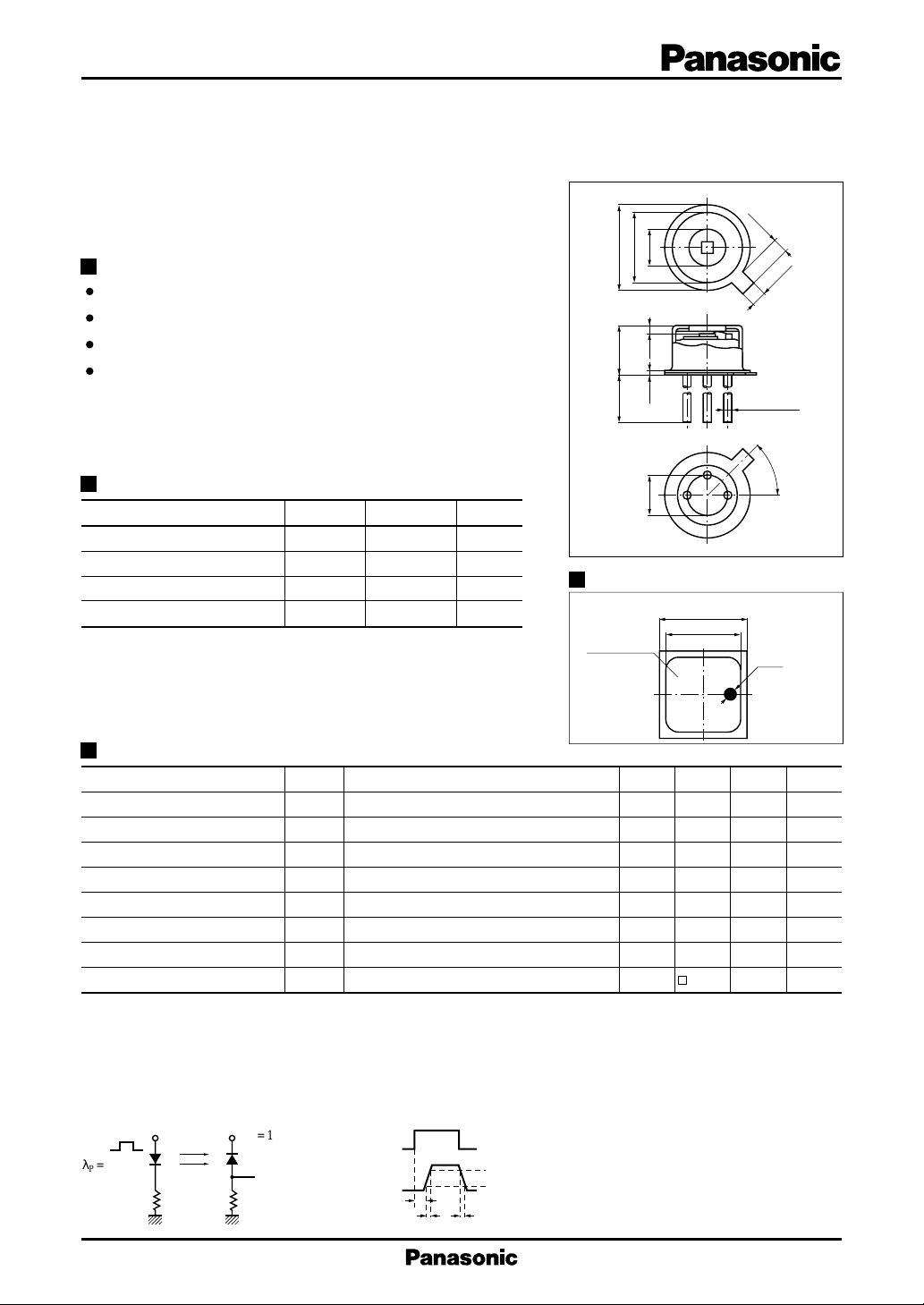
Unit : mm
1.0±0.1
ø2.4±0.1
ø5.4±0.1
ø4.6±0.05
(0.5)(0.3)
1.0±0.1
1.1
0.88
123
3-ø0.45±0.04
45±3˚
Unit : mm
A1
ø0.1
1: Anode
2: Case
3: Cathode
Absolute Maximum Ratings (Ta = 25˚C)
Parameter Symbol Ratings Unit
Reverse voltage (DC) V
Power dissipation P
Operating ambient temperature
Storage temperature T
R
D
T
– 25 to +100 ˚C
opr
– 40 to +100 ˚C
stg
14.2±0.5 3.2±0.05
ø2.54±0.25
30 V
50 mW
Dimensions of detection area
Active region
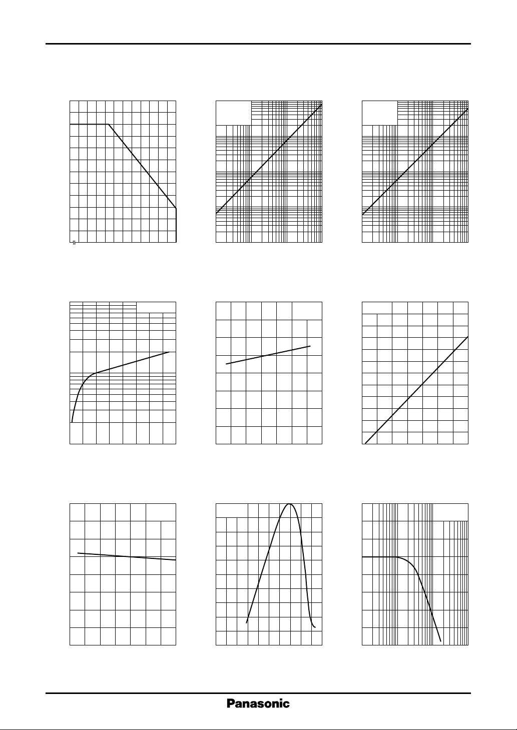
Electro-Optical Characteristics (Ta = 25˚C)
Parameter Symbol Conditions min typ max Unit
Dark current I
Photo current I
Peak sensitivity wavelength
Frequency characteristics f
Capacitance between pins C
Photodetection sensitivity R VR = 10V, λ = 800nm 0.45 0.55 A/W
Acceptance half angle θ
Photodetection surface shape
Note 1) Spectral sensitivity : Sensitivity at wavelengths exceeding 400 nm as a percentage, is 100% to maximum sensitivity.
Note 2) This product is not designed to withstand electromagnetic radiation or heavy-charge particles.
Note 3) The glass strength of this product cannot withstand loads of 0.5 kg or greater. This fact needs to be taken into consideration
if optical fibers are to be mounted on the product.
*1
Measurements were made using a tungsten lamp (color temperature T = 2856K) as a light source.
*2
Switching time measurement circuit (see figure below) Note : Detection photo current –3 dB
Sig.IN
λP = 800nm
50Ω
VR = 10V
Sig.OUT
R
L
VR = 10V 0.1 10 nA
D
VR = 10V, L = 1000 lx
L
λ
VR = 10V 900 nm
P
*2
VR = 10V, RL = 50Ω 50 MHz
C
VR = 10V 3 pF
t
Measured from the optical axis to the half power point
*1
47 µA
40 deg.
D Effective photodetection area 0.88 mm
: Delay time
t
(Input pulse)
(Output pulse)
t
d
t
r
t
f
d
: Rise time (Time required for the collector photo current
t
90%
r
to increase from 10% to 90% of its final value)
10%
: Fall time (Time required for the collector photo current
t
f
to decrease from 90% to 10% of its initial value)
1
PNZ331F PIN Photodiodes
P
60
50
(mW)
40
D
30
20
Power dissipation P
10
0
– 25
D
0 20406080100
Ambient temperature Ta (˚C )
I
D
(nA)
D
10
1
–1
— Ta
— V
R
Ta = 25˚C
2
10
V
= 10V
R
Ta = 25˚C
T = 2856K
10
(µA)
L
1
Photo current I
–1
10
–2
10
10
160
120
(%)
L
80
I
— L
L
2
10
3
10
Illuminance L (lx)
I
— Ta
L
V
= 10V
R
L = 1000 lx
T = 2856K
4
10
2
I
10
VR = 10V
Ta = 25˚C
λ = 800nm
10
(µA)
L
1
Photo current I
–1
10
–2
10
10
10
10
(nA)
D
–1
10
3
2
1
VR = 10V
11010
Incident photo power P (µW)
I
D
— P
L
— Ta
2
Dark current I
–2
10
03281624
Reverse voltage VR (V)
I
— Ta
160
120
(%)
L
80
40
Relative photo current I
0
– 40
L
– 20 0 20 60 8040 100
Ambient temperature Ta (˚C )
V
= 10V
R
L = 1000 lx
40
Relative photo current I
0
– 20 0 20 60 8040 100
– 40
Ambient temperature Ta (˚C )
Spectral sensitivity characteristics
100
V
= 10V
R
Ta = 25˚C
80
60
40
Relative sensitivity S (%)
20
0
400 600 800 1000 1200
200
Wavelength λ (nm)
–1
10
Dark current I
–2
10
–3
10
– 40 20 60 100– 20 04080
Ambient temperature Ta (˚C )
Frequency characteristics
6
4
2
0
– 2
– 4
– 6
Relative power output P (dB)
– 8
– 10
1
10 10
Frequency f (MHz)
VR = 10V
RL = 50Ω
Ta = 25˚C
2
3
10
2
 Loading...