

Panasonic PNZ331CL Datasheet

PIN Photodiodes
PNZ331CL
PIN Photodiode
For optical fiber communication systems
Features
TO-18 standard type package
High coupling capability suitable for plastic fiber
High quantum efficiency
High-speed response
Absolute Maximum Ratings (Ta = 25˚C)
Parameter Symbol Ratings Unit
Reverse voltage (DC) V
Power dissipation P
Operating ambient temperature
Storage temperature T
R
D
T
–25 to +85 ˚C
opr
–30 to +100 ˚C
stg
30 V
50 mW
Unit : mm
1.0±0.1
3-ø0.45±0.04
45±3˚
1.0±0.1
1: Anode
2: Case
3: Cathode
ø5.4±0.1
ø4.2±0.05
(0.2)
14.2±0.5 3.25±0.3
2.25±0.1
ø2.54±0.25
123
Dimensions of detection area
A1
ø0.1
Unit : mm
1.1
0.88
Active region
Electro-Optical Characteristics (Ta = 25˚C)
Parameter Symbol Conditions min typ max Unit
Dark current I
Photo current I
Peak sensitivity wavelength
Response time tr, t
Capacitance between pins C
Photodetection sensitivity R VR = 10V, λ = 800nm 0.55 A/W
Acceptance half angle θ
Photodetection surface shape
Note 1) Spectral sensitivity: Sensitivity at wavelengths exceeding 400 nm as a percentage of maximum sensitivity is 100%
Note 2) This product is not designed to withstand electromagnetic radiation or heavy-charge particles.
Note 3) Difficult to guarantee compliance with moisture resistance standard (MIL-STD-202D)
*1
Measurements were made using a tungsten lamp (color temperature T = 2856K) as a light source.
*2
Switching time measurement circuit (see figure below)
Sig.IN
λP = 800nm
50Ω
VR = 10V
Sig.OUT
R
L
VR = 10V 0.1 10 nA
D
VR = 10V, L = 1000 lx
L
λ
VR = 10V 900 nm
P
*2
VR = 10V, RL = 50Ω 2ns
f
VR = 10V 3 pF
t
Measured from the optical axis to the half power point
*1
714 µA
70 deg.
D Effective detection area 0.88 mm
: Delay time
t
(Input pulse)
(Output pulse)
t
d
t
r
t
f
d
: Rise time (Time required for the collector photo current
t
90%
r
to increase from 10% to 90% of its final value)
10%
: Fall time (Time required for the collector photo current
t
f
to decrease from 90% to 10% of its initial value)
1
PIN Photodiodes PNZ331CL
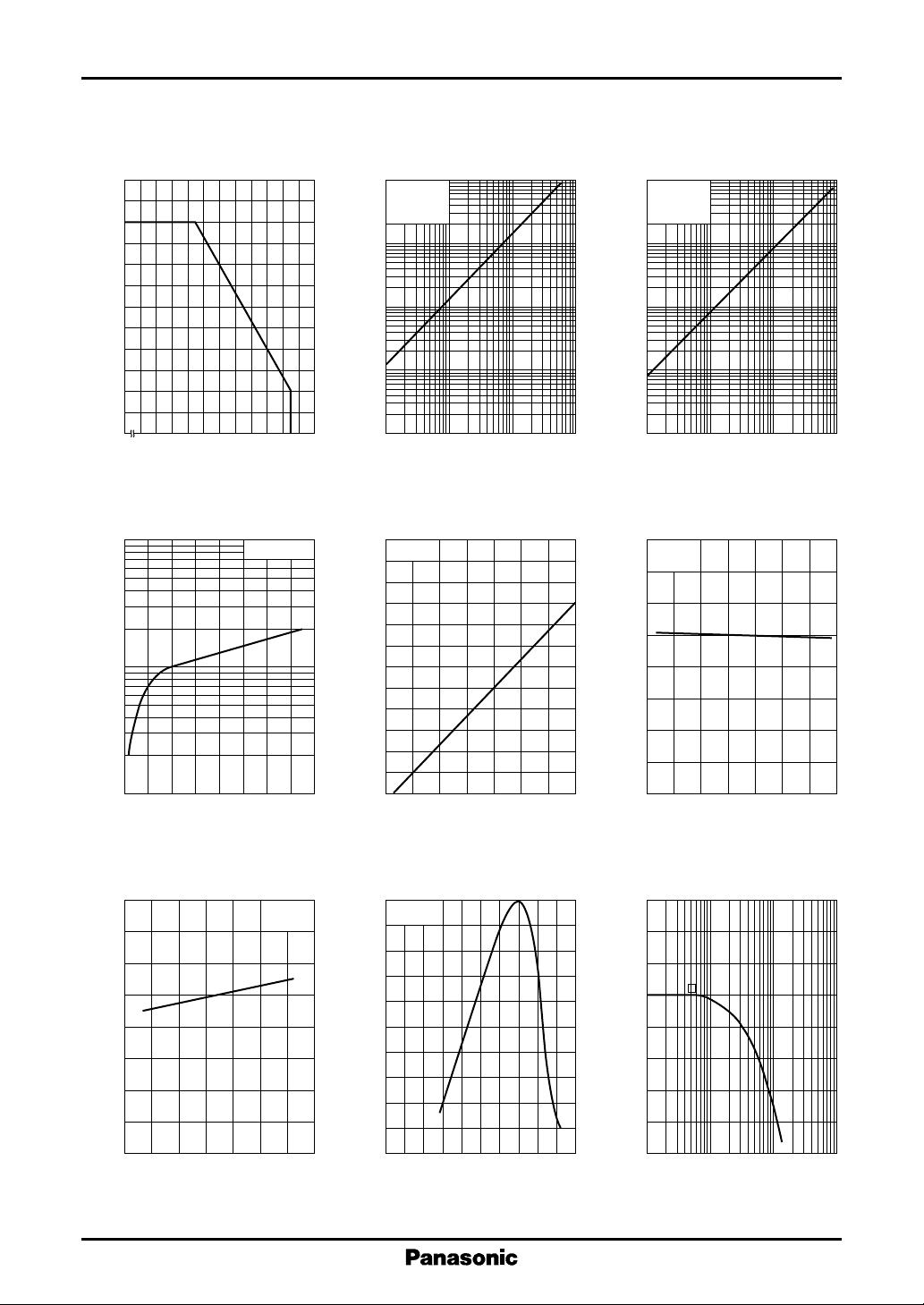
P
60
50
(mW)
40
D
30
20
Power dissipation P
10
0
– 25
D
0 20406080100
Ambient temperature Ta (˚C )
I
D
(nA)
D
10
1
–1
— Ta
— V
R
Ta = 25˚C
2
10
V
= 10V
R
Ta = 25˚C
T = 2856K
10
(µA)
L
1
Photo current I
–1
10
–2
10
10
3
10
VR = 10V
2
10
10
(nA)
D
1
I
— L
L
2
10
3
10
Illuminance L (lx)
I
— Ta
D
4
10
2
10
V
= 10V
R
Ta = 25˚C
λ = 800nm
10
(µA)
L
1
Photo current I
–1
10
–2
10
10
2
10
Incident photo power P (µW)
R — Ta
160
VR = 10V
λ = 800nm
120
80
I
L
— P
3
10
4
10
Dark current I
–2
10
03281624
Reverse voltage VR (V)
I
— Ta
160
120
(%)
L
80
40
Relative photo current I
0
– 40
L
– 20 0 20 60 8040 100
Ambient temperature Ta (˚C )
V
= 10V
R
L = 1000 lx
T = 2856K
–1
10
Dark current I
–2
10
–3
10
– 40 20 60 100– 20 04080
Ambient temperature Ta (˚C )
Spectral sensitivity characteristics
100
V
= 10V
R
Ta = 25˚C
80
60
40
20
Relative photodetection sensitivity R (%)
0
400 600 800 1000 1200
200
Wavelength λ (nm)
40
Photodetection sensitivity R (%)
0
– 40 20 60 100– 20 04080
Ambient temperature Ta (˚C )
Frequency characteristics
6
4
2
0
– 2
– 4
– 6
Relative power output P (dB)
– 8
– 10
1
Frequency f (MHz)
10 10
2
3
10
2
 Loading...