

Panasonic PNZ323B Datasheet
PIN Photodiodes
PNZ323B
PIN Photodiode
For optical control systems
Features
Fast response which is well suited to high speed modulated light
detection : t
High sensitivity, high reliability
Peak sensitivity wavelength matched with infrared light emitting
diodes : λ
Wide detection area, wide acceptance half angle : θ = 70 deg. (typ.)
Adoption of visible light cutoff resin
, tf = 50 ns (typ.)
r
= 970 nm (typ.)
P
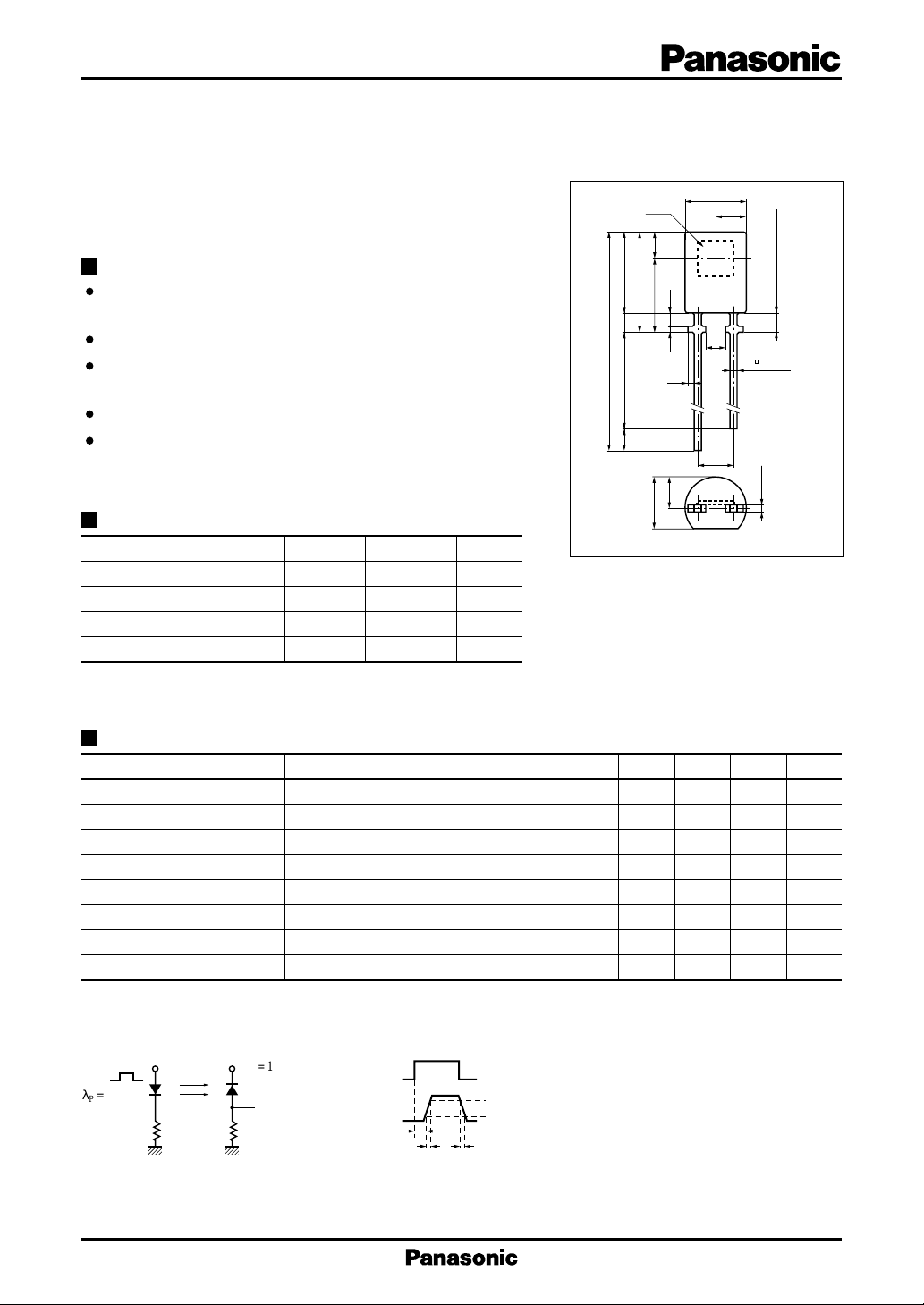
Chip
6.0±0.2
7.5±0.2
1.5±0.222.25±1.0
31.25±1.0
(1.5)
4.6±0.2
2.3
(2)
5.5±0.2
1.32
0.5 1.0
0.5
2.54
Unit : mm
Not soldered 1.5 max.
2- 0.6±0.1
Absolute Maximum Ratings (Ta = 25˚C)
Parameter Symbol Ratings Unit
Reverse voltage (DC) V
Power dissipation P
Operating ambient temperature
Storage temperature T
R
D
T
opr
stg
30 V
100 mW
–30 to +85 ˚C
– 40 to +100 ˚C
Electro-Optical Characteristics (Ta = 25˚C)
Parameter Symbol Conditions min typ max Unit
Dark current I
Photo current I
Sensitivity to infrared emitters
S
Peak sensitivity wavelength
Response time tr, t
Response time tr, t
Capacitance between pins C
Acceptance half angle θ
*1
Measurements were made using a tungsten lamp (color temperature T = 2856K) as a light source.
*2
Light source : λ = 940 nm
*3
Switching time measurement circuit
VR = 10V 5 50 nA
D
VR = 10V, L = 1000 lx
L
*2
VR = 5V, H = 0.1mW/cm
IR
λ
VR = 10V 970 nm
P
*3
VR = 10V, RL = 1kΩ 50 ns
f
*3
VR = 10V, RL = 100kΩ 5 µs
f
VR = 0V, f = 1MHz 70 pF
t
*1
2
Measured from the optical axis to the half power point
(2.3)
3.8±0.2
12
0.6±0.1
1: Anode
2: Cathode
31 µA
3.2 4 µA
70 deg.
λP = 800nm
50Ω
Sig.IN
VR = 10V
Sig.OUT
R
L
(Input pulse)
(Output pulse)
: Delay time
t
d
: Rise time (Time required for the collector photo current
t
90%
r
to increase from 10% to 90% of its final value)
t
d
t
r
10%
: Fall time (Time required for the collector photo current
t
t
f
f
to decrease from 90% to 10% of its initial value)
1
PIN Photodiodes PNZ323B
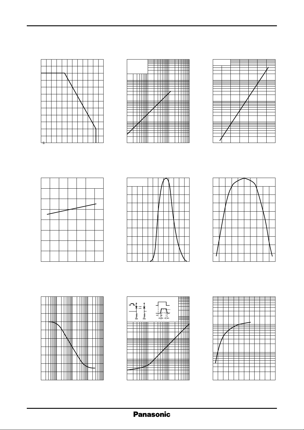
I
— Ta
D
120
100
(mW)
80
D
60
P
D
— Ta
I
— L
3
10
V
R
Ta = 25˚C
T = 2856K
2
10
(µA)
L
10
L
= 10V
10
10
(nA)
D
10
3
2
VR = 10V
40
Power dissipation P
20
0
0 20406080100
– 30
Ambient temperature Ta (˚C )
I
— Ta
160
140
120
(%)
L
100
80
60
40
Relative photo current I
20
0
– 40
L
– 20 0 20 60 8040 100
Ambient temperature Ta (˚C )
= 10V
V
R
L = 1000 lx
T = 2856K
Photo current I
1
–1
10
10
2
10
3
10
Illuminance L (lx)
Spectral sensitivity characteristics
100
V
= 10V
R
Ta = 25˚C
80
60
40
Relative sensitivity S (%)
20
0
700 800 900 1000 1100 1200
600
Wavelength λ (nm)
Dark current I
1
–1
10
4
10
– 40 20 60 100– 20 04080
100
80
60
40
Relative sensitivity S (%)
20
0
Ambient temperature Ta (˚C )
Directional characteristics
Ta = 25˚C
80 40 0 40 80
Angle θ (deg.)
C
100
80
(pF)
t
60
40
20
Capacitance between pins C
0
–2
10
t
–1
10
Reverse voltage VR (V)
2
— V
R
11010
2
tr , t
— R
2
10
Sig.IN
50Ω
10
(µs)
f
, t
r
1
–1
10
VR = 10V
Sig.
OUT
R
L
f
trt
Rise time, Fall time t
–2
10
–1
10
11010
External load resistance RL (kΩ)
I
— V
D
L
90%
10%
t
d
f
10
10
(nA)
D
2
1
R
Dark current I
2
0 16324882440
–1
10
Reverse voltage VR (V)
 Loading...