

Panasonic PNZ312D Datasheet

PIN Photodiodes
R1 = R
2
R
1
R
2
+10V
PNZ312D
Dual Division Silicon PIN Photodiode
For optical information systems
Features
Fast response : tr, tf = 10 ns (typ.)
Good photo current linearity
Low dark current : ID = 20 nA (max.)
Small size plastic package (flat type)
Adoption of visible light cutoff resin
Applications
Auto focus sensor for still cameras and video cameras etc.
Distance measuring systems
Position sensor for automatic assembly lines
Eye sensor for industrial robots
Absolute Maximum Ratings (Ta = 25˚C)
Parameter Symbol Ratings Unit
Reverse voltage (DC) V
Power dissipation P
Operating ambient temperature
T
Storage temperature T
R
D
opr
stg
30 V
30 mW
–25 to +85 ˚C
–30 to +100 ˚C
Unit : mm
1.0±0.2
ø3.2 Dep. 0.1(typ.)
1.0
0.6
0.2
5˚
1: Anode A
2: Common Cathode
3: Anode B
4: Common Cathode
1.8±0.3
10˚
10˚
+0.1
0.2
–0.05
13.5±1.0
4.0±0.1
4-0.6
4-0.5±0.1
5.0±0.1
2.54±0.1
43
A
1.0±0.3 1.0±0.1
+0.1
–0.2
12
10˚
5˚
B
1.0
10˚
Note) The PNZ312D package consists of a visible
light cutoff resin. Therefore the chips (A and B)
shown in the drawing cannot actually be seen.
Dimensions of detection area
Unit : mm
1.35
3.5
1.6
AB
1.0
1.6
0.04
Electro-Optical Characteristics (Ta = 25˚C)
Parameter Symbol Conditions min typ max Unit
Reverse voltage (DC) V
Dark current I
Photo current I
Peak sensitivity wavelength
Response time tr, t
Capacitance between pins C
Acceptance half angle θ
Note) The indicated values for absolute maximum ratings and electro-optical characteristics are the values
corresponding to individual elements.
*1
Measurements were made using a white tungsten lamp (color temperature T = 2856K) as a light source.
*2
Semiconductor laser light source ( λ = 800 nm )
IR = 10µA30V
R
VR = 10V 20 nA
D
*3
VR = 10V, L = 1000 lx
L
λ
VR = 10V 940 nm
P
*2
VR = 10V, RL = 1kΩ 10 ns
f
VR = 10V, f = 1MHz 5 pF
t
Measured from the optical axis to the half power point
*1
812 µA
65 deg.
*3
Photo current measurement circuit
1
PNZ312D PIN Photodiodes
P
40
30
(mW)
D
20
10
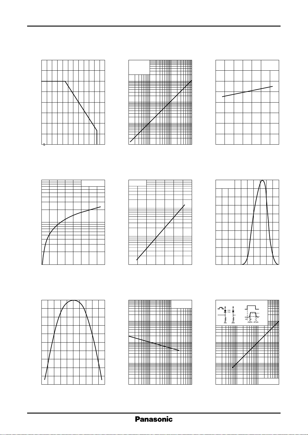
Power dissipation P
0
– 25
D
0 20406080100
Ambient temperature Ta (˚C )
I
D
(nA)
D
10
1
–1
Dark current I
— Ta
— V
R
Ta = 25˚C
3
10
V
= 10V
R
Ta = 25˚C
T = 2856K
2
10
(µA)
L
10
Photo current I
1
–1
10
10
10
VR = 10V
1
(nA)
D
–1
10
Dark current I
I
— L
L
2
10
3
10
Illuminance L (lx)
I
— Ta
D
160
140
120
(%)
L
100
80
60
40
Relative photo current I
20
4
10
0
– 40
Spectral sensitivity characteristics
100
80
60
40
Relative sensitivity S (%)
20
I
— Ta
L
= 10V
V
R
L = 1000 lx
T = 2856K
– 20 0 20 60 8040 100
Ambient temperature Ta (˚C )
= 10V
V
R
Ta = 25˚C
–2
10
0 12202832481624
Reverse voltage VR (V)
Directivity characteristics
100
80
60
40
Relative sensitivity S (%)
20
0
80 40 0 40 80
Angle θ (deg.)
2
–2
10
– 40 20 60 100– 20 04080
Ambient temperature Ta (˚C )
C
— V
t
10
(pF)
t
10
3
2
10
1
R
f = 1MHz
Ta = 25˚C
Capacitance between pins C
–1
10
–1
10
11010
Reverse voltage VR (V)
0
200
4
10
3
10
(ns)
f
, t
r
2
10
10
Rise time, Fall time t
2
1
10
400 600 800 1000 1200
Wavelength λ (nm)
tr , t
— R
f
L
VR=10V
Sig.IN
t
d
trt
90%
10%
f
Ta = 25˚C
Sig.
OUT
R
50Ω
–1
L
11010
External load resistance RL (kΩ)
2
 Loading...