

Panasonic PNZ109L Datasheet
Phototransistors
PNZ109L
Silicon NPN Phototransistor
For optical control systems
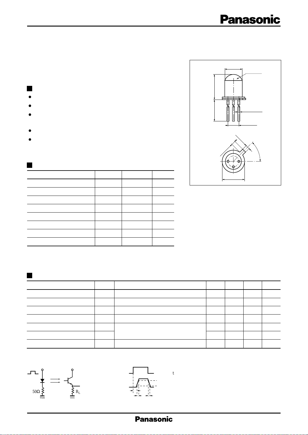
ø4.6±0.15
Unit : mm
Glass lens
Features
High sensitivity : I
Built-in filter to cutoff visible light for reducing ambient light noise
Peak sensitivity wavelength matched with infrared light emitting
devices : λ
= 900 nm (typ.)
p
Fast response : tr = 5 µs (typ.)
Long lifetime, high reliability
= 3.5 mA (min.) (at L = 100 lx)
CE(L)
Absolute Maximum Ratings (Ta = 25˚C)
Parameter Symbol Ratings Unit
Collector to emitter voltage
Collector to base voltage
Emitter to collector voltage
Emitter to base voltage
Collector current I
Collector power dissipation
Operating ambient temperature
Storage temperature T
V
CEO
V
CBO
V
ECO
V
EBO
C
P
C
T
opr
stg
20 V
30 V
3V
5V
30 mA
150 mW
–25 to +85 ˚C
–30 to +100 ˚C
6.3±0.3
12.7 min.
1.0±0.15
1.0±0.2
3
1
2
ø5.75 max.
3-ø0.45±0.05
2.54±0.25
45±3˚
1: Emitter
2: Base
2: Collector
Electro-Optical Characteristics (Ta = 25˚C)
Parameter Symbol Conditions min typ max Unit
Dark current I
Collector photo current I
Peak sensitivity wavelength
CEO
CE(L)
λ
Acceptance half angle θ
Rise time t
Fall time t
Collector saturation voltage
*1
Measurements were made using a tungsten lamp (color temperature T = 2856K) as a light source.
*2
Switching time measurement circuit
Sig.IN
50Ω R
V
CC
L
Sig.OUT
V
CE(sat)ICE(L)
(Input pulse)
(Output pulse)
VCE = 10V 0.05 2 µA
VCE = 10V, L = 100 lx
VCE = 10V 900 nm
P
*1
Measured from the optical axis to the half power point
*2
VCC = 10V, I
r
*2
RL = 100Ω 6 µs
f
= 1mA, L = 500 lx
t
d
t
r
= 5mA 5 µs
CE(L)
*1
td : Delay time
: Rise time (Time required for the collector photo current to
t
90%
r
increase from 10% to 90% of its final value)
10%
: Fall time (Time required for the collector photo current to
t
t
f
f
decrease from 90% to 10% of its initial value)
3.5 mA
10 deg.
0.3 0.6 V
1
Phototransistors PNZ109L
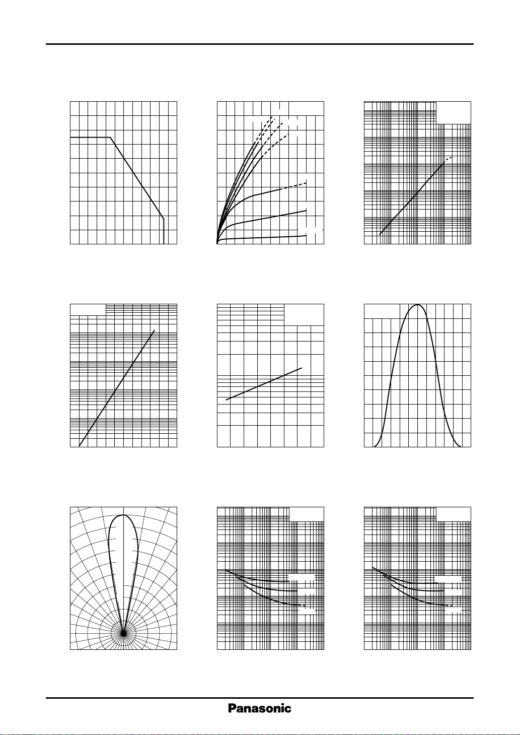
P
— Ta
200
160
(mW)
C
120
80
40
C
Collector power dissipation P
0
0 20406080100
– 20
Ambient temperature Ta (˚C )
I
— Ta
CEO
VCE = 10V
(µA)
CEO
10
2
10
10
1
–1
I
— V
20
1000 lx
16
(mA)
CE(L)
12
8
4
Collector photo current I
0
02016812424
CE(L)
500 lx
CE
300 lx
200 lx
Ta = 25˚C
T = 2856K
100 lx
50 lx
L = 10 lx
3
10
2
(mA)
10
CE(L)
10
1
–1
10
Collector photo current I
–2
10
1
Collector to emitter voltage VCE (V)
Spectral sensitivity characteristics
100
V
Ta = 25˚C
80
60
40
10
(mA)
CE(L)
10
I
— Ta
2
CE(L)
VCE = 10V
L = 100 lx
T = 2856K
I
CE(L)
10 10
Illuminance L (lx)
= 10V
CE
10
— L
2
VCE = 10V
Ta = 25˚C
T = 2856K
3
4
10
Dark current I
–2
10
–3
10
– 20 0 40 8020 60 100
Ambient temperature Ta (˚C )
Directivity characteristics
0˚ 10˚ 20˚
100
90
80
70
60
50
Relative sensitivity S (%)
40
30
Collector photo current I
1
– 40 0 40 80 120
Ambient temperature Ta (˚C )
4
10
30˚
40˚
50˚
60˚
70˚
80˚
90˚
3
10
(µs)
r
2
10
10
Rise time t
1
–1
10
–2
Collector photo current I
Relative sensitivity S (%)
20
0
700 800 900 1000 1100 1200
600
Wavelength λ (nm)
t
— I
r
CE(L)
VCC = 10V
Ta = 25˚C
RL = 1kΩ
500Ω
100Ω
–1
10
10 10
110
CE(L)
2
(mA)
4
10
3
10
(µs)
2
f
10
10
Fall time t
1
–1
10
–2
Collector photo current I
t
— I
f
CE(L)
VCC = 10V
Ta = 25˚C
RL = 1kΩ
500Ω
100Ω
–1
10
10 10
110
CE(L)
2
(mA)
2
 Loading...