

Panasonic MAZ3120D Datasheet
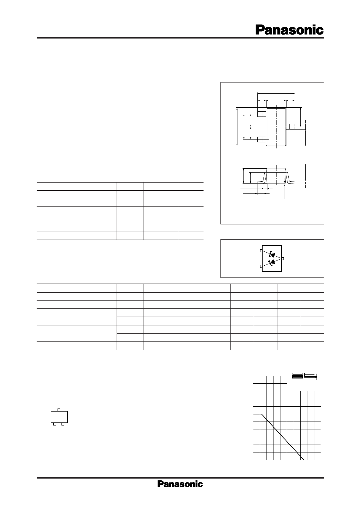
■ Internal Connection
1 : Cathode 1
2 : Cathode 2
3 : Anode 1
Anode 2
Mini Type Package (3-pin)
Unit : mm
Unit
V
V
Ω
Ω
µA
µA
mV/˚C
Condition
I
F
=10mA
I
Z
= 5mA
I
Z
= 0.5mA
I
Z
= 5mA
V
R
= 8.0V
V
R
= 10.9V
I
Z
= 5mA
■ Marking
Symbol
V
F
VZ*
2
R
ZK
R
Z
I
R1
I
R2
SZ*
3
Note 1. Rated input/output frequency : 5MHz
2. * 1 : The VZ value is for the temperature of 25˚C. In other cases, carry out the temperature compensation.
* 2 : Guaranteeed at 20ms after power application
* 3 : Tj= 25 to 150˚C
■ Electrical Characteristics (Ta= 25˚C)
*
1
*1Working value in a single piece
*2 With a printed-circuit board
*3t=100µ s, Tj=150˚C
Unit
mA
mA
mW
W
˚C
˚C
Rating
100 *
1
200 *
1
100 *
1
15
150
– 55 to + 150
Symbol
I
F(AV)
I
FRM
P
tot
*
2
P
ZSM
*
3
T
j
T
stg
MA3100WA
Silicon planer type
Constant voltage, constant current, waveform
cripper and surge absorption circuit
■ Features
●
Mini type package (3-pin)
●
Two anode-common wiring of MA3120
■ Absolute Maximum Ratings (Ta= 25˚C)
Parameter
Average forward current
Instanious forward current
Total power dissipation
Non-repetitive reverse surge power dissipation
Junction temperature
Storage temperature
1
2
3
Zener Diodes Composite Elements MA111
2.8
+0.2
–0.3
1.5
+0.25
–0.05
0.65±0.15 0.65±0.15
3
1
2
0.950.95
1.9±0.2
0.4
+0.1
–0.05
1.1
+0.2
–0.1
0.8
0.4±0.2
0 to 0.1
0.16
+0.1
–0.06
1.45
0.1 to 0.3
2.9
+0.2
–0.05
Parameter
Forward voltage
Zener voltage
Operating resistance
Reverse current
Temperature coefficient of zener voltage
min
11.4
6.0
typ
0.8
12.0
10
8.4
max
0.9
12.7
170
25
0.1
60
8.4
12A
P
tot
– Ta
Ambient temperature Ta (˚C
)
Power dissipation P
tot
(
mW
)
0
0 2001601208040
50
150
100
200
10mm
0.8mm
10mm
Cu foil t=0.035 mm
With a printed-circuit board
A
K
 Loading...