

Panasonic MAZ3100D Datasheet
MA3100WA
Silicon planer type
Constant voltage, constant current, waveform
cripper and surge absorption circuit
■ Features
●
Mini type package (3-pin)
●
Two anode-common wiring of MA3100
■ Absolute Maximum Ratings (Ta= 25˚C)
Unit
V
V
Ω
Ω
µA
µA
mV/˚C
Condition
I
F
=10mA
I
Z
= 5mA
I
Z
= 0.5mA
I
Z
= 5mA
V
R
= 7V
V
R
= 8.9V
I
Z
= 5mA
Note 1. Rated input/output frequency : 5MHz
2. * 1 : The VZ value is for the temperature of 25˚C. In other cases, carry out the temperature compensation.
* 2 : Guaranteeed at 20ms after power application
* 3 : Tj= 25 to 150˚C
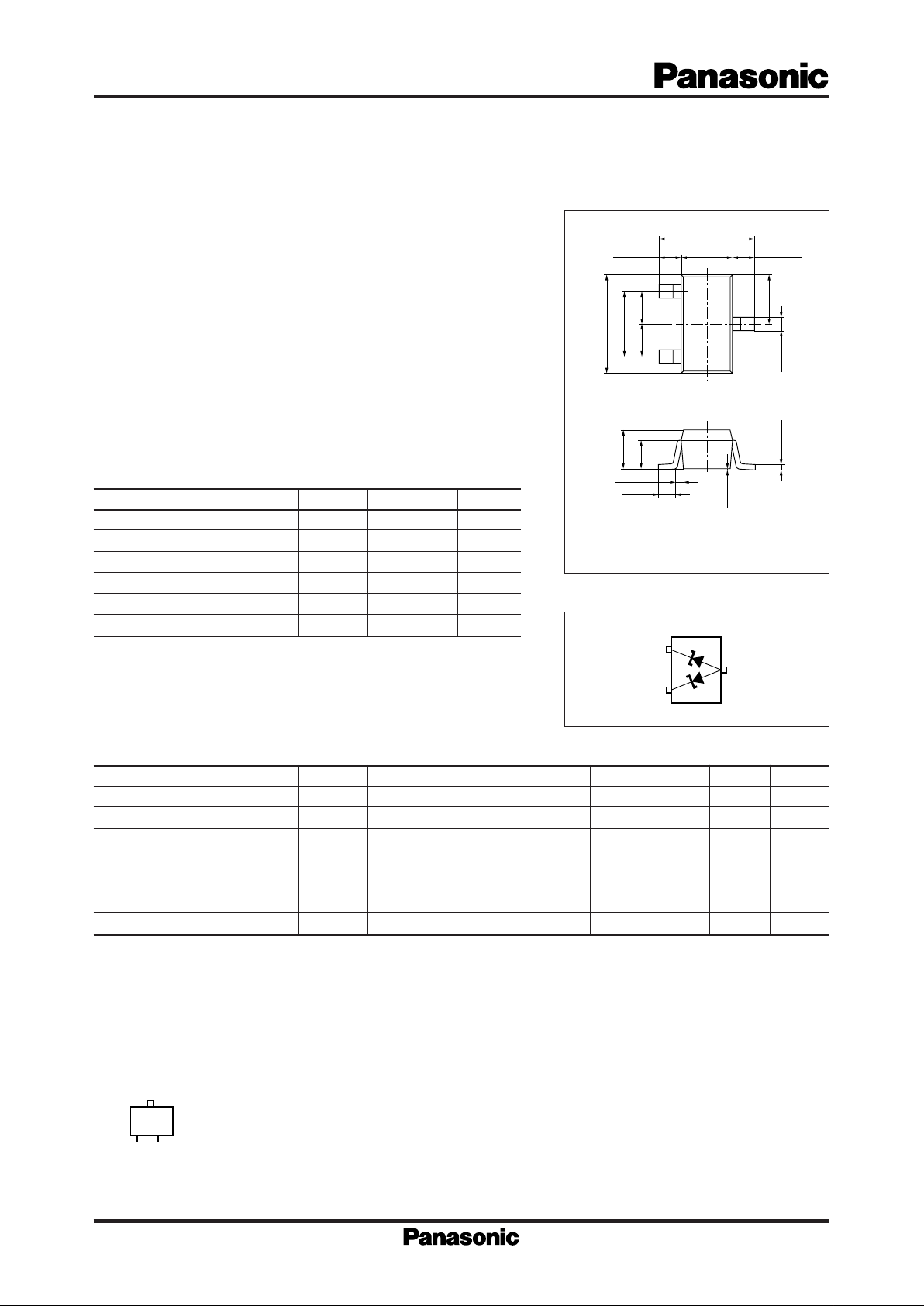
■ Marking
Symbol
V
F
VZ*
2
R
ZK
R
Z
I
R1
I
R2
SZ*
3
Unit
mA
mA
mW
W
˚C
˚C
Symbol
I
F(AV)
I
FRM
P
tot
*
2
P
ZSM
*
3
T
j
T
stg
■ Electrical Characteristics (Ta= 25˚C)
*
1
■ Internal Connection
Unit : mm
1 : Cathode 1
2 : Cathode 2
3 : Anode 1
Anode 2
Mini Type Package (3-pin)
Parameter
Average forward current
Instanious forward current
Total power dissipation
Non-repetitive reverse surge power dissipation
Junction temperature
Storage temperature
Rating
100 *
1
200 *
1
100 *
1
15
150
– 55 to + 150
1
2
3
Zener Diodes Composite Elements MA111
*1Working value in a single piece
*2 With a printed-circuit board
*3t=100µ s, Tj=150˚C
2.8
+0.2
–0.3
1.5
+0.25
–0.05
0.65±0.15 0.65±0.15
3
1
2
0.950.95
1.9±0.2
0.4
+0.1
–0.05
1.1
+0.2
–0.1
0.8
0.4±0.2
0 to 0.1
0.16
+0.1
–0.06
1.45
0.1 to 0.3
2.9
+0.2
–0.05
Parameter
Forward voltage
Zener voltage
Operating resistance
Reverse current
Temperature coefficient of zener voltage
min
9.40
4.5
typ
0.8
6.4
max
0.9
10.60
130
20
0.2
60
8.0
10A
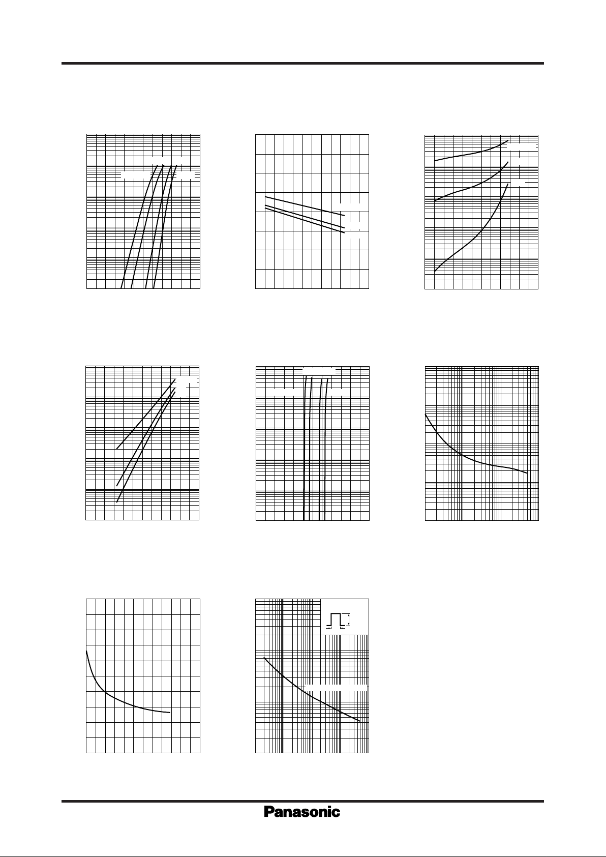
P
ZSM
– t
W
Ct – V
R
IR – Ta IZ – V
Z
RZ – I
Z
IR – V
R
VF – TaIF – V
F
Zener Diodes Composite Elements MA3100WA
10
–5
0 0.2 0.4 0.6 0.8 1.0 1.2
10
–4
10
–3
10
–2
10
–1
1
Forward voltage V
F
(V)
Forward curren I
F
(
A
)
Ta=150˚C
100˚C
–20˚C
25˚C
Ambient temperature Ta (˚C
)
Forward voltage V
F
(
V
)
0
0.2
0.4
0.6
0.8
1.0
1.2
1.4
1.6
–40 0 40 80 120 160 200
IF=100mA
10mA
3mA
Reverse voltage V
R
(V)
Reverse current I
R
(
A
)
10
–13
024681012
10
–12
10
–11
10
–10
10
–9
10
–8
Ta=150˚C
25˚C
100˚C
Ambient temperature Ta (˚C
)
Reverse current I
R
(
nA
)
0.1
–40 0 40 80 120 160 200
1
10
100
1000
10000
VR=7V
3V
1V
10
–6
7 8 9 10 11 12 13
10
–5
10
–4
10
–3
10
–2
10
–1
Ta=–20˚C 150˚C
25˚C 100˚C
Zener voltage V
Z
(V)
Zener current I
Z
(
A
)
Operating resistance R
Z
(R)
Zener current I
Z
(A)
10
–1
10
–4
1
10
10
2
10
3
10
–3
10
–2
10
–1
Reverse voltage VR (V
)
Terminal capacitance C
t
(
pF
)
0
20
40
60
80
100
024681012
Pulse width t
W
(ms)
Non-repetitive reverse
surge power dissipation
P
ZSM
(
W
)
1
0.01
10
100
1000
0.1 101 100
Ta=25˚C
t
P
ZSM
Breakdown point (typ)
 Loading...