

Panasonic MA6X718 Datasheet
Schottky Barrier Diodes (SBD)
2.8
+ 0.2
− 0.3
1.5
+ 0.25
− 0.05
0.65 ± 0.15 0.65 ± 0.15
1
6
5
4
3
2
1.45 ± 0.1
0.95 0.95
1.9 ± 0.1
0.3
+ 0.1
− 0.05
0.5
+ 0.1
− 0.05
2.9
+ 0.2
− 0.05
1.1
+ 0.2
− 0.1
0.8
0.4 ± 0.2
0 to 0.05
0.16
+ 0.1
− 0.06
0.1 to 0.3
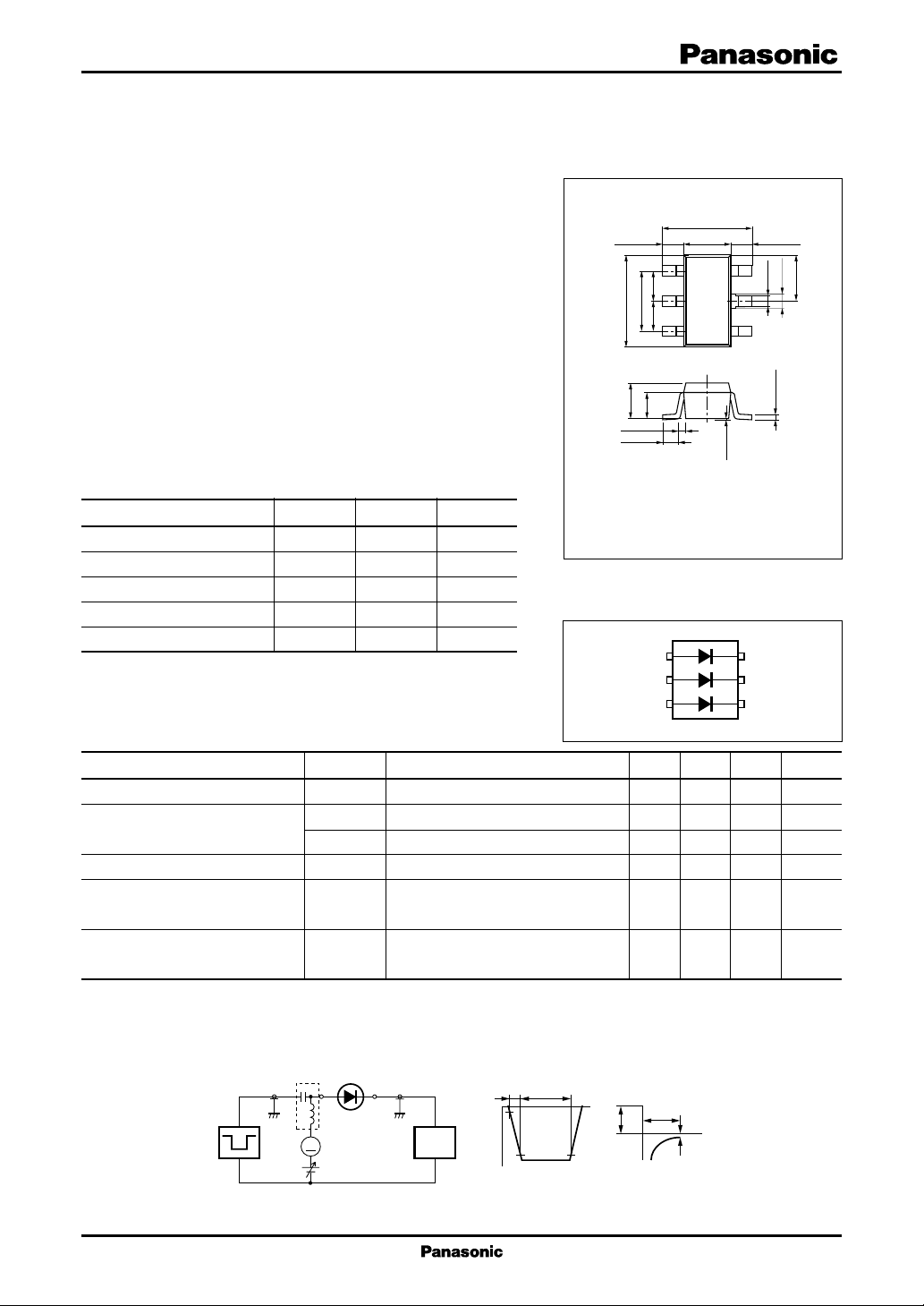
MA6X718
Silicon epitaxial planar type
For switching circuits
For wave detection circuit
■ Features
•
Three MA3X704As in the same direction are contained in one
package
•
Optimum for low-voltage rectification because of its low forward
rise voltage (V
•
Optimum for high-frequency rectification because of its short reverse recovery time (t
)
F
)
rr
Unit : mm
■ Absolute Maximum Ratings Ta = 25°C
Parameter Symbol Rating Unit
Reverse voltage (DC) V
Peak forward current
Forward current (DC)
Junction temperature T
Storage temperature T
Note) * : Value in per diode
■ Electrical Characteristics Ta = 25°C
Parameter Symbol Conditions Min Typ Max Unit
Reverse current (DC) I
Forward voltage (DC) V
Terminal capacitance C
Reverse recovery time
Detection efficiency η Vin = 3 V
Note) 1. Schottky barrier diode is sensitive to electric shock (static electricity, etc.). Due attention must be paid on the charge of a
human body and the leakage of current from the operating equipment
2. Rated input/output frequency: 2 000 MHz
3. * : trr measuring instrument
1 : Cathode 1
2 : Cathode 2
*
*
R
I
FM
I
F
j
stg
30 V
150 mA
30 mA
125 °C
−55 to +125 °C
Marking Symbol: M2N
Internal Connection
3 : Cathode 3
Mini Type Package (6-pin)
6
5
4
R
F1
V
F2
*
t
rr
VR = 30 V 1 µA
IF = 1 mA 0.4 V
IF = 30 mA 1.0 V
VR = 1 V, f = 1 MHz 1.5 pF
t
IF = IR = 10 mA 1.0 ns
4 : Anode 3
5 : Anode 2
6 : Anode 1
1
2
3
Irr = 1 mA, RL = 100 Ω
, f = 30 MHz 65 %
(peak)
RL = 3.9 kΩ, CL = 10 pF
Bias Application Unit N-50BU
Pulse Generator
(PG-10N)
= 50 Ω
R
s
A
W.F.Analyzer
(SAS-8130)
= 50 Ω
R
i
Input Pulse Output Pulse
t
t
p
r
10%
90%
V
R
t
p
= 0.35 ns
t
r
δ = 0.05
t
= 2 µs
I
F
= 10 mA
I
F
= 10 mA
I
R
= 100 Ω
R
L
t
rr
I
= 1 mA
rr
t
1
MA6X718
Schottky Barrier Diodes (SBD)
IF V
3
10
2
10
)
mA
(
Ta = 125°C
F
10
1
Forward current I
−1
10
−2
10
0 0.2 0.4 0.6 0.8 1.0 1.2
F
Forward voltage VF (V
Ct V
2.4
2.0
)
pF
(
t
1.6
1.2
0.8
Terminal capacitance C
0.4
R
75°C 25°C
− 20°C
f = 1 MHz
= 25°C
T
a
VF T
IR T
a
a
IF = 30 mA
10 mA
1 mA
VR = 30 V
3 V
1 V
)
1.0
0.8
)
V
(
F
0.6
0.4
Forward voltage V
0.2
0
)
−40 0 40 80 120 160
Ambient temperature Ta (°C
3
10
2
10
)
µA
(
R
10
1
Reverse current I
−1
10
3
10
2
10
)
µA
(
R
10
1
Reverse current I
−1
10
−2
10
0 5 10 15 20 25 30
IR V
R
Ta = 125°C
Ambient temperature VR (V
75°C
25°C
)
0
0 5 10 15 20 25 30
Reverse voltage VR (V
2
−2
10
)
−40 0 40 80 120 160 200
Ambient temperature Ta (°C
)
 Loading...