Panasonic MA3X730 Datasheet

Schottky Barrier Diodes (SBD)
MA3X730
Silicon epitaxial planar type
For UHF mixer
Unit : mm
+ 0.2
2.8
− 0.3
+ 0.25
1.5
0.65 ± 0.15 0.65 ± 0.15
− 0.05
■ Features
•
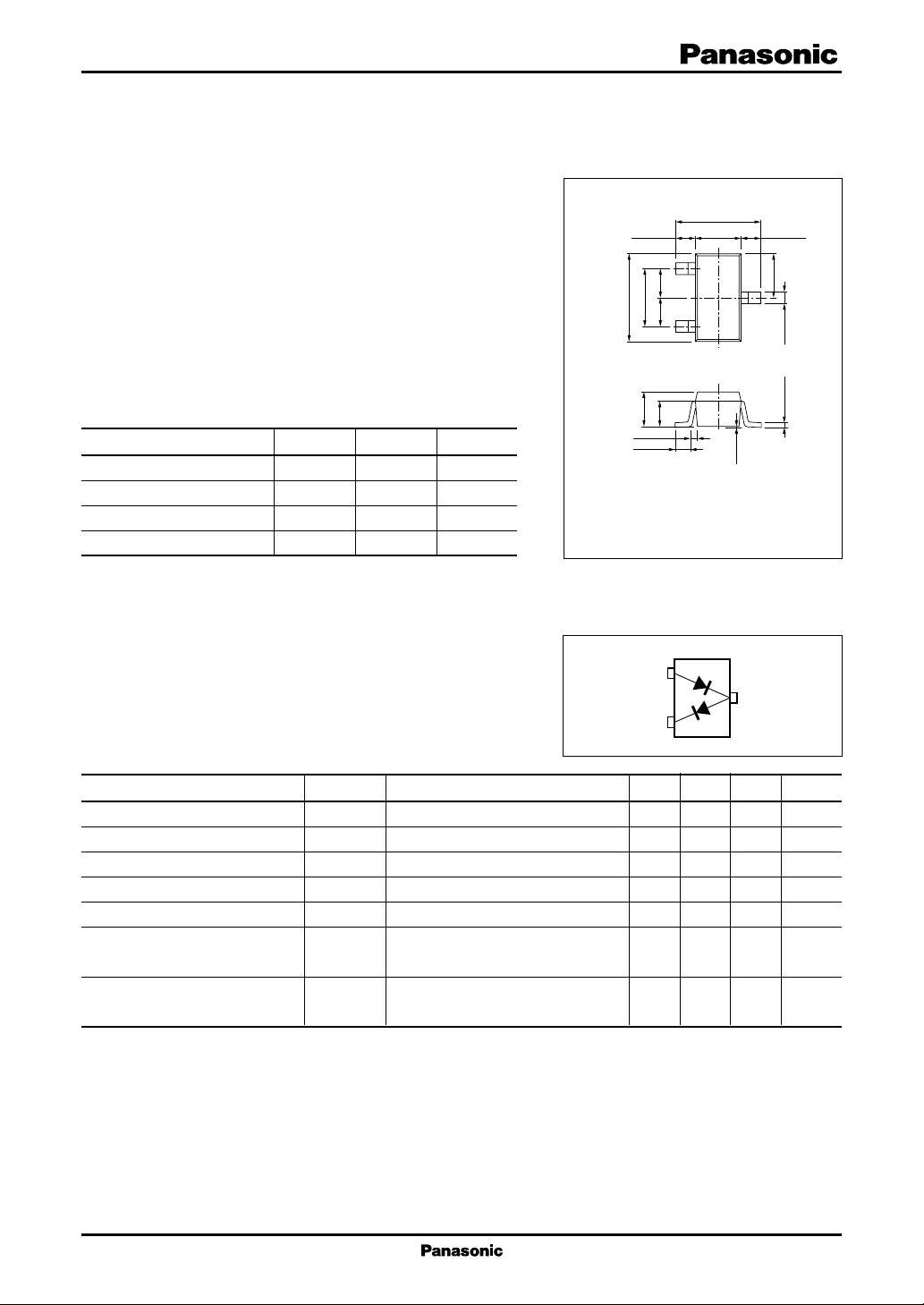
Two MA2X707s are contained in the (Mini (3-pin) type)
•
Large conversion gain (GC)
•
Small forward voltage V
•
Optimum for the UHF band mixer
F
■ Absolute Maximum Ratings Ta = 25°C
Parameter Symbol Rating Unit
Forward voltage (DC) V
Reverse voltage (DC) V
Junction temperature T
Storage temperature T
F
R
j
stg
0.5 V
5V
125 °C
−55 to +125 °C
+ 0.2
− 0.05
2.9
1.9 ± 0.2
− 0.1
+ 0.2
1.1
0.1 to 0.3
0.4 ± 0.2
1 : Anode 1
2 : Cathode 2
3 : Cathode 1
Anode 2
1
0.950.95
2
0.8
0 to 0.1
Mini Type Package (3-pin)
1.45
3
− 0.05
+ 0.1
0.4
− 0.06
+ 0.1
0.16
JEDEC : TO-236
EIAJ : SC-59
Marking Symbol: M2X
Internal Connection
1
3
2
■ Electrical Characteristics Ta = 25°C
Parameter Symbol Conditions Min Typ Max Unit
Forward current (DC) I
Reverse current (DC) I
F
R
Forward voltage (DC) V
Reverse breakdown voltage (DC) V
(BR)R
Terminal capacitance C
1,2
Conversion gain
*
GC RF = 890 MHz, LO = 935 MHz −7 −5dB
Static breakdown strength C = 100 pF, Breakdown judgment 100 200 V
Note) 1. Schottky barrier diode is sensitive to electric shock (static electricity, etc.). Due attention must be paid on the charge of a
human body and the leakage of current from the operating equipment
2. Rated input/output frequency: 935 MHz
3. Noise index is 8.5 dB
4. Each characteristic is a standard for individual diodes
5. *1: Judgement is to be made per each chip lot. Sampling of LTPD = 20% and n = 11 is guaranteed.
*2: Set min. GC = −7 dB. Out-spec products, if any, this specification would be reviewed
VF = 0.5 V 35 100 mA
VR = 5 V 35 µA
IF = 2 mA 0.25 V
F
IR = 1 mA 5 V
VR = 0.5 V, f = 1 MHz 0.65 0.85 1.05 pF
t
IF = 45 MHz
point IR ≥ 35 µA
1

MA3X730
Schottky Barrier Diodes (SBD)
IF V
100
)
10
mA
(
F
1
0.1
Forward current I
0.01
0 0.2 0.4 0.6 0.8 1.0
F
Forward voltage VF (V
Ta = 25°C
)
IR V
100
)
10
µA
(
R
1
0.1
Reverse current I
0.01
012345
R
Ta = 25°C
Reverse voltage VR (V
Ct V
100
)
pF
10
(
t
1
0.1
Terminal capacitance C
0.01
0.01
)
0.1 1 10
Reverse voltage VR (V
R
f = 1 MHz
T
= 25°C
a
)
2
 Loading...