

Panasonic MA3X153A, MA3X153 Datasheet
Switching Diodes
MA3X153, MA3X153A
Silicon epitaxial planar type
For switching circuits
+ 0.2
2.8
− 0.3
+ 0.25
− 0.05
0.65 ± 0.15 0.65 ± 0.15
1.5
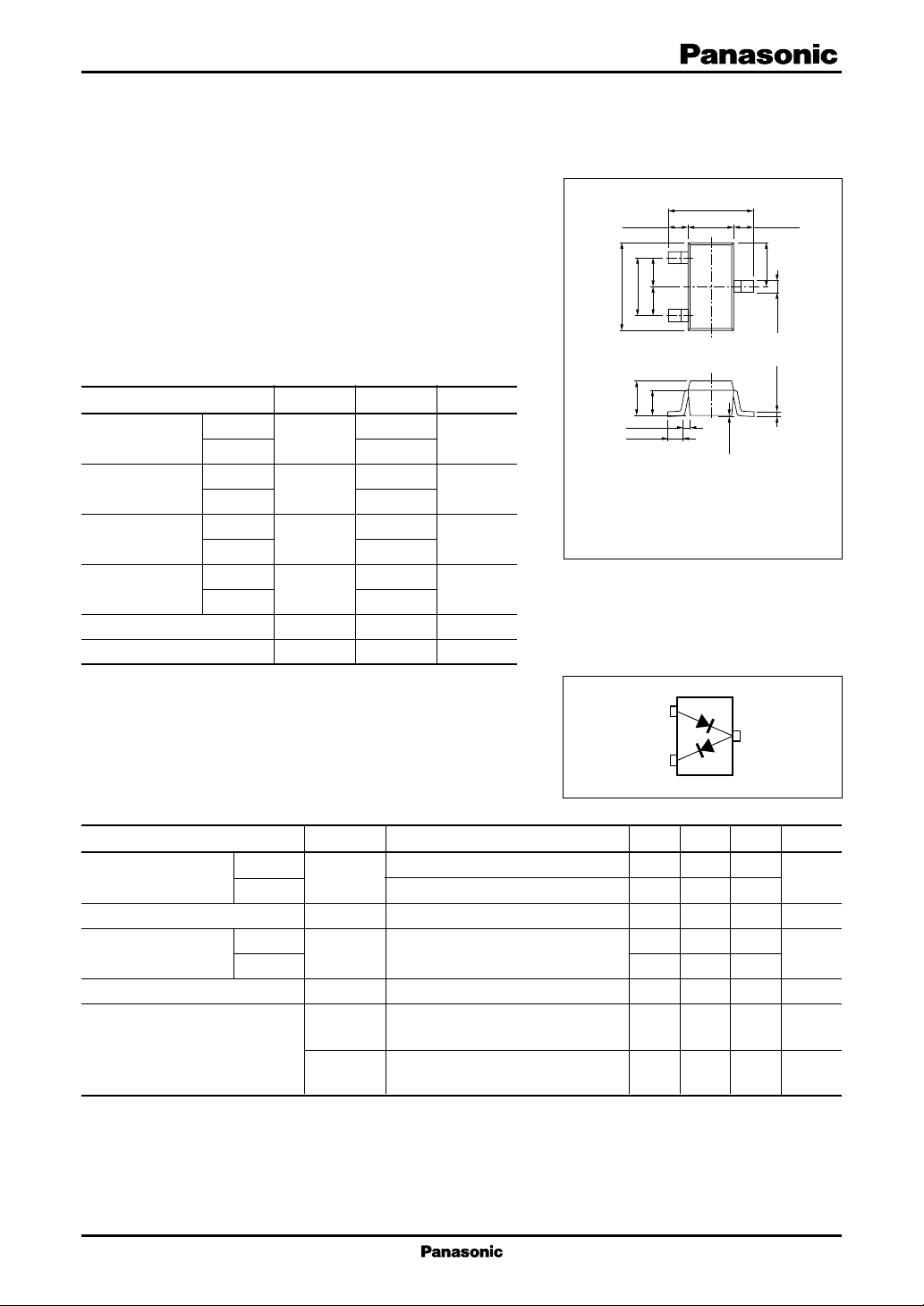
Unit : mm
■ Features
•
Small terminal capacitance, C
•
Two diodes are connected in series in the package
t
■ Absolute Maximum Ratings Ta = 25°C
Parameter Symbol Rating Unit
Reverse voltage
(DC)
Peak reverse
voltage
Forward current
(DC)
Peak forward
current
MA3X153
MA3X153A
MA3X153
MA3X153A
Single I
Series 65
Single I
Series 130
Junction temperature T
Storage temperature T
V
R
V
RM
F
FM
j
stg
100
200
150 °C
−55 to +150 °C
40
80
40
80
V
V
mA
mA
1
0.950.95
− 0.05
+ 0.2
2.9
1.9 ± 0.2
2
− 0.1
+ 0.2
0.8
1.1
0.1 to 0.3
0.4 ± 0.2
1 : Anode 1
2 : Cathode 2
3 : Anode 2
Cathode 1
Marking Symbol
• MA3X153 : MC
• MA3X153A : MP
Internal Connection
1
2
1.45
3
− 0.05
+ 0.1
0.4
− 0.06
+ 0.1
0.16
0 to 0.1
JEDEC : TO-236
EIAJ : SC-59
Mini Type Package (3-pin)
3
■ Electrical Characteristics Ta = 25°C
Parameter Symbol Conditions Min Typ Max Unit
Reverse current (DC)
Forward voltage (DC) V
Reverse voltage (DC)
Terminal capacitance C
Reverse recovery time t
Note) 1. Rated input/output frequency: 100 MHz
2. *1: Between pins 2 and 3
*2: Between pins 1 and 3
MA3X153
MA3X153A
MA3X153
MA3X153A
I
R
F
V
R
t
1
*
rr
2
*
t
rr1
VR = 40 V 0.1 µA
VR = 75 V 0.1
IF = 100 mA 1.2 V
IR = 100 µA40V
80
VR = 0 V, f = 1 MHz 5 pF
IF = 10 mA, VR = 6 V 150 ns
Irr = 0.1 · IR, RL = 100 Ω
IF = 10 mA, VR = 6 V 9 ns
Irr = 0.1 · IR, RL = 100 Ω
1
MA3X153, MA3X153A
Switching Diodes
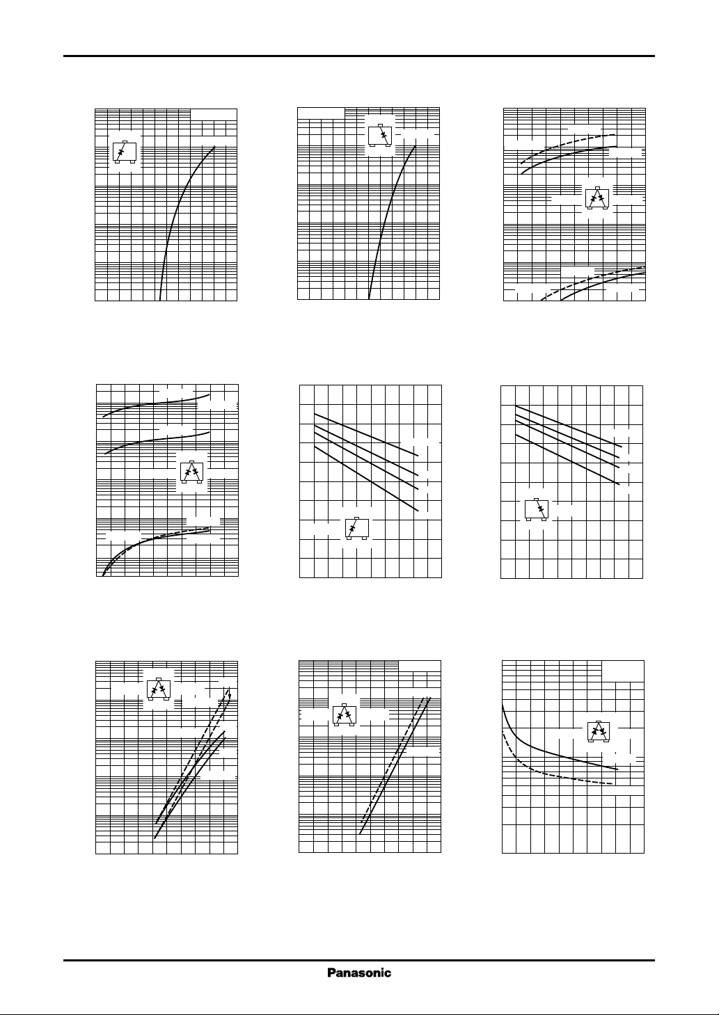
IF V
3
10
D1 (1-3)
2
10
)
mA
(
F
10
Forward current I
10
10
3
1
2
1
−1
−2
0 0.2 0.4 0.6 0.8 1.0 1.2
F
Ta = 25°C
D
Forward voltage VF (V
V
R
10
)
1
µA
(
R
−1
10
−2
10
Reverse current I
Ta = 25°C
−3
10
0 20406080100
D1 (1-3)
D2 (3-2)
3
1
D1 (1-3)
D2 (3-2)
Ta = 125°C
D
2
Reverse voltage VR (V
(1-3)
1
2
IF V
D2 (3-2)
3
1
VF T
3
1
2
F
2
a IR
(3-2)
D
2
)
IF = 10 mA
3 mA
1 mA
0.1 mA
3
10
Ta = 125°C
2
10
)
µA
(
R
10
1
Reverse current I
−1
10
−2
10
0 1020304050
1.0
0.8
)
V
(
F
0.6
0.4
Forward voltage V
0.2
0
−40 0 40 80 120 160
)
3
10
Ta = 25°C
2
10
)
mA
(
F
10
1
Forward current I
−1
10
−2
10
0 0.2 0.4 0.6 0.8 1.0 1.2
)
)
(
(3-2)D1 (1-3)
)
Forward voltage VF (V
1.0
0.8
V
F
0.6
0.4
(1-3)
D
Forward voltage V
1
0.2
0
−40 0 40 80 120 160
Ambient temperature Ta (°C
IR V
R
D1 (1-3
)
D2 (3-2
3
D
2
1
2
D1 (1-3)
Ta = 25°C
D2 (3-2)
Reverse voltage VR (V
VF T
a
IF = 10 mA
3
(3-2)
D
2
1
2
0.1 mA
Ambient temperature Ta (°C
)
(3-2)D1 (1-3)
)
3 mA
1 mA
)
2
10
10
)
nA
(
R
1
−1
10
Reverse current I
−2
10
−3
10
−40 0 40 80 120
Ambient temperature Ta (°C
2
1
T
3
2
a
D
(3-2)D1 (1-3)
2
VR = 80 V
D1 (1-3)
D2 (3-2)
40 V
80 V
40 V
IR T
2
D2 (3-2
a IR
V
= 40 V
R
D
(1-3)
1
)
D
(3-2)
2
5
)
pF
(
3
t
2
1
0.5
0.3
Terminal capacitance C
0.2
0.1
0 1020304050
)
3
10
2
10
)
µA
(
R
10
1
Reverse current I
−1
10
−2
10
)
3
D
(1-3
)
1
1
−40 0 40 80 120
Ambient temperature Ta (°C
Ct V
R
f = 1 MHz
T
(
)
1-3
D
1
132
D
D
Reverse voltage VR (V
= 25°C
a
(
D
2
(
3-2
2
(
1-3
1
)
)
3-2
)
)
 Loading...