

Panasonic MA2SV02 Datasheet
Variable Capacitance Diodes
MA2SV02
Silicon epitaxial planar type
For VCO
■ Features
•
Good linearity and large capacitance-ratio in C
•
Small series resistance r
•
SS-mini type package, allowing downsizing of equipment and
D
automatic insertion through the taping package
■ Absolute Maximum Ratings Ta = 25°C
Parameter Symbol Rating Unit
Reverse voltage (DC) V
Junction temperature T
Storage temperature T
R
j
stg
VR relation
D
6V
150 °C
−55 to +150 °C
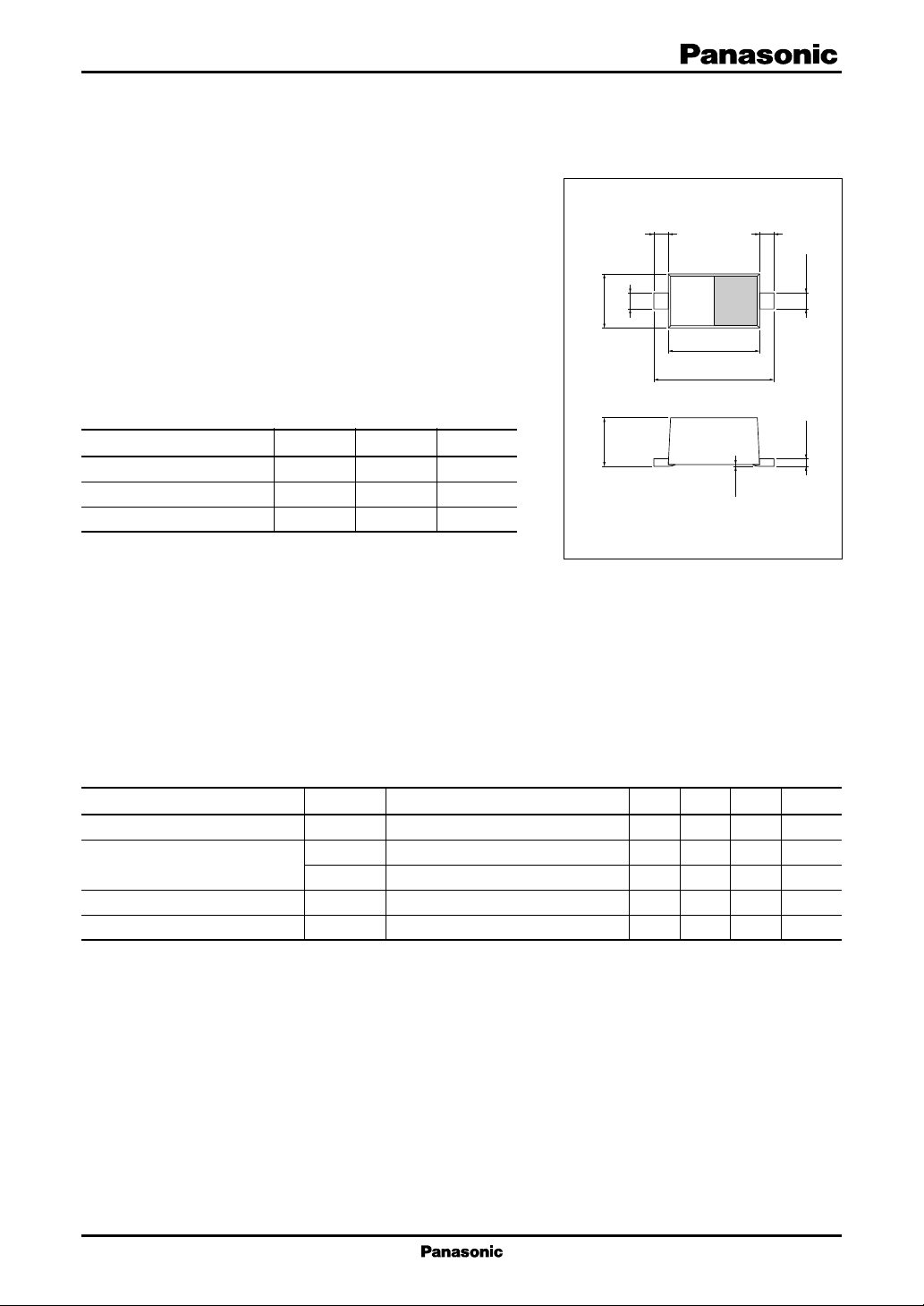
Unit : mm
0.15 min.
− 0.02
+ 0.05
0.8 ± 0.10.7 ± 0.1
0.27
SS-Mini Type Package (2-pin)
1.3 ± 0.1
1.7 ± 0.1
0 to 0.1
0.15 min.
− 0.02
+ 0.05
0.27
− 0.02
+ 0.05
0.13
1 : Anode
2 : Cathode
Marking Symbol: 3
■ Electrical Characteristics Ta = 25°C
Parameter Symbol Conditions Min Typ Max Unit
Reverse current (DC) I
Diode capacitance C
Capacitance ratio
Series resistance
*
R
D(1V)
C
D(4V)
C
D(1V)/CD(4V)
r
D
Note) 1.Rated input/output frequency: 470 MHz
2.*: rf measuring instrument: YHP MODEL 4191A RF IMPEDANCE ANALYZER
VR = 5 V 10 nA
VR = 1 V, f = 1 MHz 18.0 20.0 pF
VR = 4 V, f = 1 MHz 7.3 9.0 pF
VR = 4 V, f = 470 MHz 0.3 Ω
2.1 2.6
1
MA2SV02
Variable Capacitance Diodes
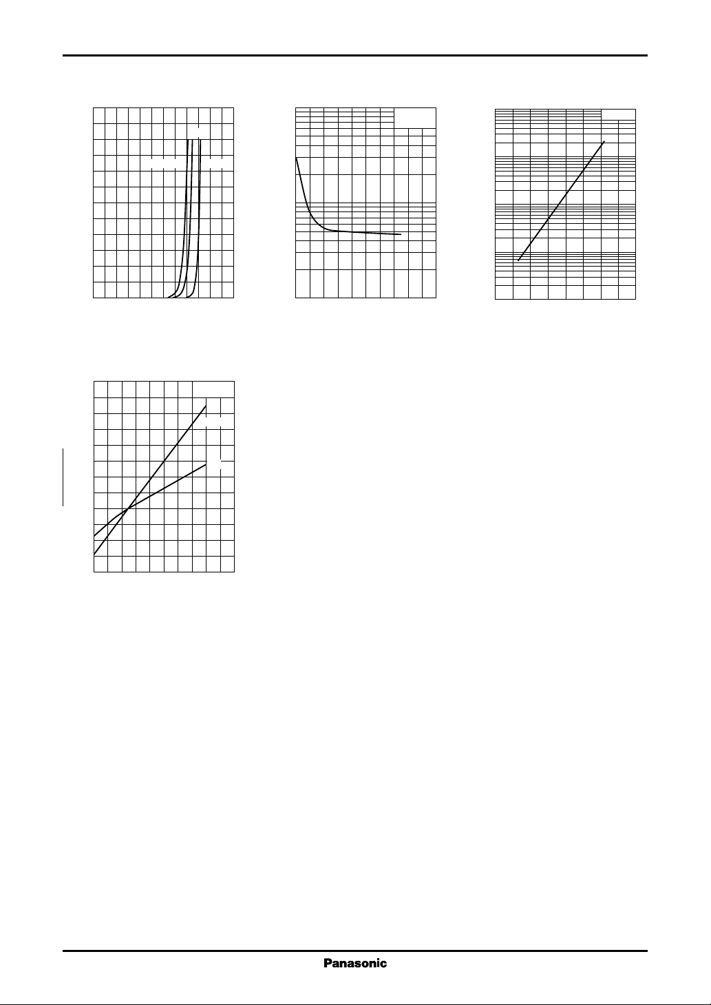
120
IF V
100
)
mA
(
80
F
60
40
Forward current I
20
0
0 0.2 0.4 0.6 0.8 1.0 1.2
1.04
1.03
1.02
)
)
a
T
(
1.01
= 25°C
D
a
C
T
(
D
C
1.00
Ta = 60°C
Forward voltage VF (V
CD T
F
25°C
a
− 40°C
)
f = 1 MHz
VR = 1 V
4 V
100
CD V
50
)
pF
30
(
D
20
10
5
3
Diode capacitance C
2
1
0 8 16 24 324 1220283640
R
f = 1 MHz
= 25°C
T
a
Reverse voltage VR (V
IR T
100
)
10
nA
(
R
1
0.1
Reverse current I
0.01
)
0 40 80 120 16020 60 100 140
Ambient temperature Ta (°C
a
VR = 5 V
)
0.99
0.98
0 20 40 60 80 100
Ambient temperature Ta (°C
)
2
 Loading...