

Panasonic MA2SD10 Datasheet
Schottky Barrier Diodes (SBD)
MA2SD10
Silicon epitaxial planar type
For super-high speed switching circuit
■ Features
•
Sealed in the super small SS-mini type 2-pin package
•
Allowing to rectify under (I
•
Low forward rise voltage V
•
Allowing high-density mounting
= 200 mA) condition
F(AV)
F
■ Absolute Maximum Ratings Ta = 25°C
Parameter Symbol Rating Unit
Reverse voltage (DC) V
Repetitive peak reverse voltage
Non-repetitive peak forward I
surge current
*
Peak forward current I
Average forward current I
Junction temperature T
Storage temperature T
V
F(AV)
R
RRM
FSM
FM
j
stg
Note) * : The peak-to-peak value in one cycle of 50 Hz sine-wave
(non-repetitive)
20 V
20 V
1A
300 mA
200 mA
125 °C
−55 to +125 °C
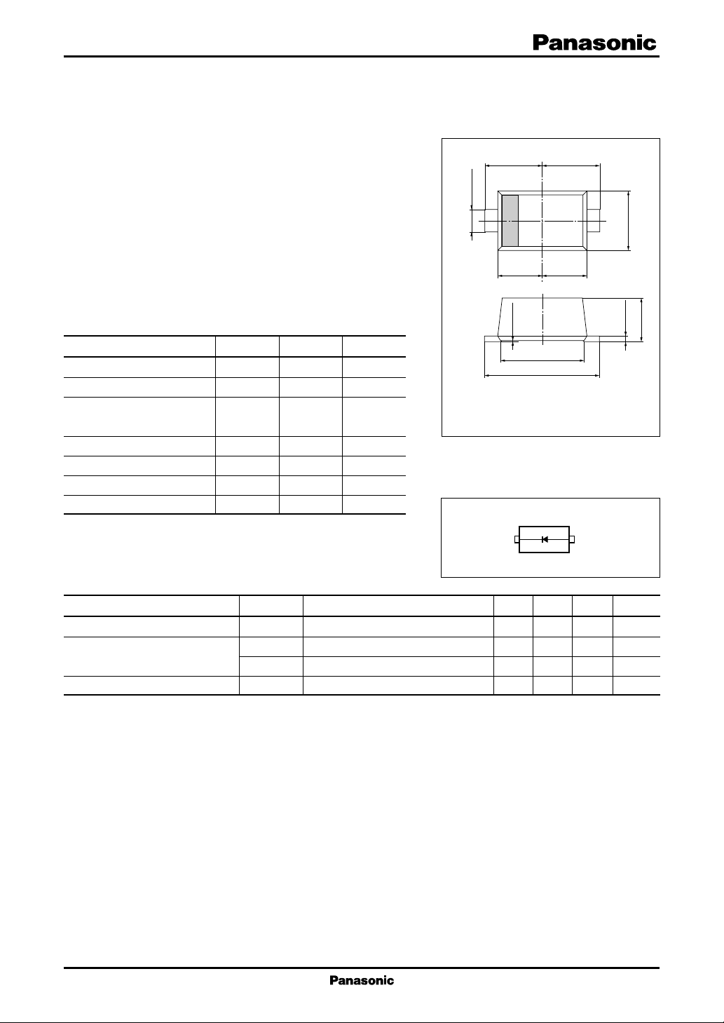
0.80
0.30 ± 0.05
0.60
0.01 ± 0.01
+ 0.05
1.20
− 0.03
1.60 ± 0.05
SS-Mini Type Package (2-pin)
Marking Symbol: 2L
Internal Connection
21
0.80 ± 0.05
0.60
Unit : mm
+ 0.05
12
+ 0.05
− 0.02
0.12
1 : Anode
2 : Cathode
− 0.03
0.80
+ 0.05
− 0.03
0.60
■ Electrical Characteristics Ta = 25°C ± 3°C
Parameter Symbol Conditions Min Typ Max Unit
Reverse current (DC) I
Forward voltage (DC) V
R
F1
V
F2
Terminal capacitance C
Note) 1. Schottky barrier diode is sensitive to electric shock (static electricity, etc.). Due attention must be paid on the charge of
a human body and the leakage of current from the operating equipment.
2. Rated input/output frequency: 250 MHz
VR = 10 V 20 µA
IF = 5 mA 0.27 V
IF = 200 mA 0.47 V
VR = 0 V, f = 1 MHz 40 pF
t
1
MA2SD10
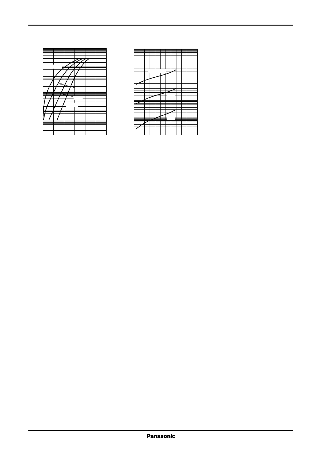
Schottky Barrier Diodes (SBD)
IF V
1
−1
10
Ta = 125°C
)
A
(
−2
10
F
−3
10
−4
10
F
75°C
25°C
− 20°C
Forward current I
−5
10
−6
10
0 0.1 0.2 0.3 0.4 0.5 0.6
Forward voltage VF (V
IR V
−1
10
−2
10
)
A
(
R
−3
10
−4
10
Reverse current I
−5
10
−6
10
)
Ta = 125°C
0 5 10 15 20 25 30
Reverse voltage VR (V
R
75°C
25°C
)
2
 Loading...