

Band Switching Diodes
MA2S077
Silicon epitaxial planar type
For band switching
■ Features
•
Low forward dynamic resistance r
•
Less voltage dependence of diode capacitance C
•
SS-mini type package, allowing downsizing of equipment and
automatic insertion through the taping package
■ Absolute Maximum Ratings Ta = 25°C
Parameter Symbol Rating Unit
Reverse voltage (DC) V
Forward current (DC) I
Operating ambient temperature*T
Storage temperature T
Note) * : Maximum ambient temperature during operation
f
R
F
−25 to +85 °C
opr
−55 to +150 °C
stg
D
35 V
100 mA
0.15 min.
− 0.02
+ 0.05
0.8 ± 0.10.7 ± 0.1
0.27
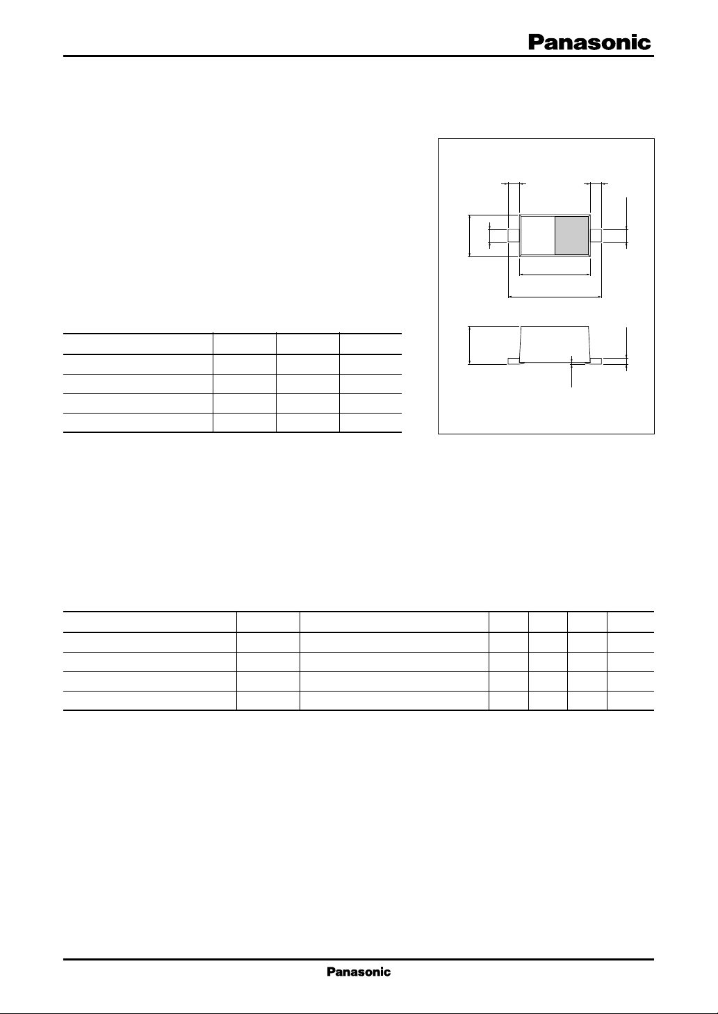
SS-Mini Type Package (2-pin)
Marking Symbol: S
1.3 ± 0.1
1.7 ± 0.1
0 to 0.1
0.15 min.
1 : Anode
2 : Cathode
Unit : mm
− 0.02
+ 0.05
0.27
− 0.02
+ 0.05
0.13
■ Electrical Characteristics Ta = 25°C
Parameter Symbol Conditions Min Typ Max Unit
Reverse current (DC) I
R
Forward voltage (DC) V
Diode capacitance C
Forward dynamic resistance
*
r
f
Note) 1.Rated input/output frequency: 100 MHz
2.*: rf measuring instrument: YHP MODEL 4191A RF IMPEDANCE ANALYZER
VR = 33 V 0.01 100 nA
IF = 100 mA 0.92 1.0 V
F
VR = 6 V, f = 1 MHz 0.9 1.2 pF
D
IF = 2 mA, f = 100 MHz 0.65 0.85 Ω
1
MA2S077
Band Switching Diodes
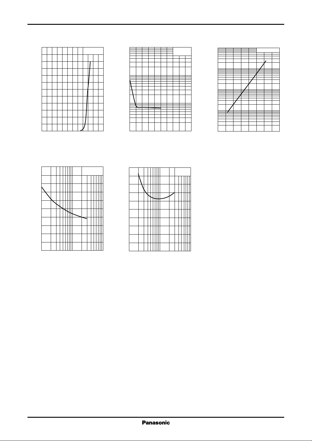
IF V
120
100
F
)
mA
(
80
F
60
40
Forward current I
20
0
0 0.2 0.4 0.6 0.8 1.0 1.2
Forward voltage VF (V
I
rf
1.0
)
Ω
(
0.8
f
0.6
F
Ta = 25°C
)
f = 100 MHz
= 25°C
T
a
100
50
30
)
20
pF
(
10
D
5
3
2
1
0.5
Diode capacitance C
0.3
0.2
0.1
0 8 16 24 4036324 122028
Reverse voltage VR (V
rf f
1.0
)
Ω
(
0.8
f
0.6
CD V
R
f = 1 MHz
= 25°C
T
a
)
IF = 2 mA
= 25°C
T
a
IR T
1 000
)
100
nA
(
R
10
1
Reverse current I
0.1
0 40 80 120 16020 60 100 140
Ambient temperature Ta (°C
a
VR = 33 V
)
0.4
0.2
Forward dynamic resistance r
0
1103 30 100
Forward current IF (mA
0.4
0.2
Forward dynamic resistance r
0
)
10 10030 300 1 000
Frequency f (MHz
)
2
 Loading...