

Panasonic MA2J1150G User Manual
This product complies with the RoHS Directive (EU 2002/95/EC).
Switching Diodes
MA2J1150G
Silicon epitaxial planar type
For small power current rectification
■ Features
• S-mini type package, allowing high-density mounting
• High reverse voltage V
R
■ Absolute Maximum Ratings Ta = 25°C
Parameter Symbol Rating Unit
Reverse voltage V
Maximum peak reverse voltage V
Output current I
Repetitive peak forward current I
Non-repetitive peak forward I
surge current
Junction temperature T
Storage temperature T
Note)*: t = l s
*
R
RM
O
FRM
FSM
j
stg
200 V
200 V
200 mA
600 µA
1A
150 °C
−55 to +150 °C
■ Package
•
Code
SMini2-F3
•
Pin Name
1: Anode
2: Cathode
■ Marking Symbol: 1F
■ Electrical Characteristics Ta = 25°C ± 3°C
Parameter Symbol Conditions Min Typ Max Unit
Forward voltage V
Reverse current I
Terminal capacitance C
Note) 1. Measuring methods are based on JAPANESE INDUSTRIAL STANDARD JIS C 7031 measuring methods for diodes.
2. Absolute frequency of input and output is 3 MHz.
F
R
IF = 200 mA 1.2 V
VR = 200 V 200 nA
VR = 0 V, f = 1 MHz 4.5 pF
t
Publication date: November 2007 SKF00094AED
1
MA2J1150G
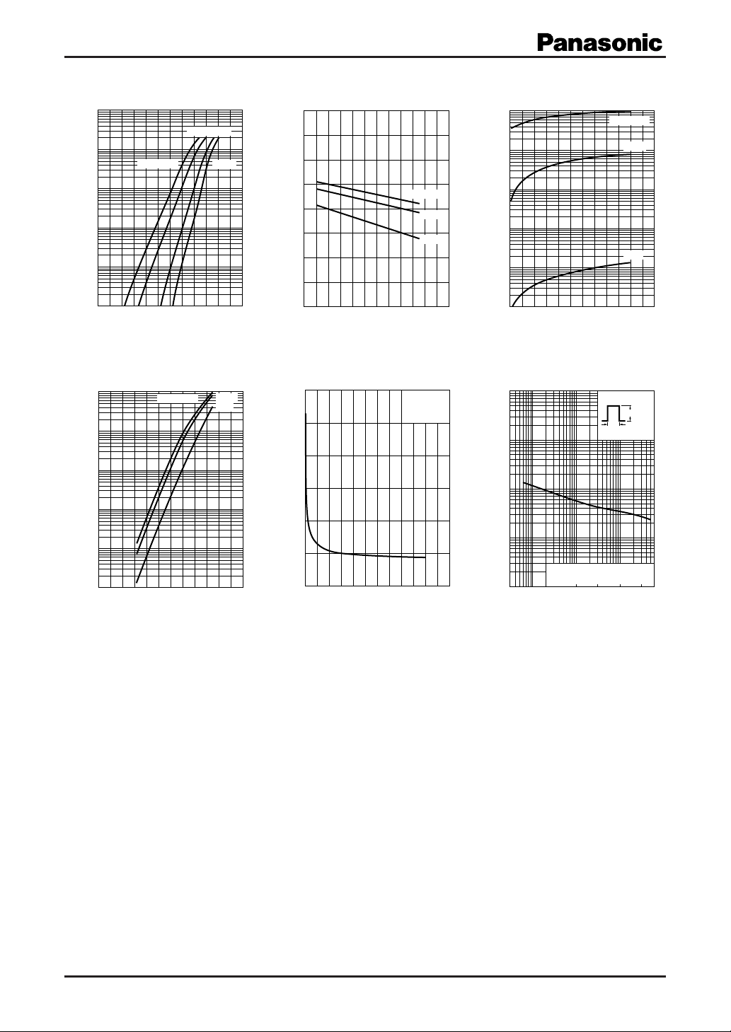
3
10
2
10
Ta = 150°C
(mA)
F
10
1
Forward current I
−1
10
I
F
This product complies with the RoHS Directive (EU 2002/95/EC).
V
F
100°C 25°C
−20°C
1.6
1.2
(V)
F
0.8
Forward voltage V
0.4
VF T
a
IF = 200 mA
10 mA
3 mA
2
10
10
)
nA
(
R
1
−1
10
Reverse current I
−2
10
IR V
R
Ta = 150°C
100°C
25°C
−2
10
0 0.2 0.4 0.6 0.8 1.0 1.2
Forward voltage VF (V)
IR T
2
10
10
)
nA
(
R
1
−1
10
Reverse current I
−2
10
−3
10
−40 0 40 80 120 160 200
a
VR = 200 V 100 V
Ambient temperature Ta (°C
10 V
0
−40 0 40 80 120 160 200
Ambient temperature Ta (°C
Ct V
3
(pF)
t
2
1
R
f = 1 MHz
= 25°C
T
a
)
Terminal capacitance C
0
0 40 80 120 160 200 240
)
Reverse voltage VR (V
)
−3
10
0 40 80 120 160 200 240
Reverse voltage VR (V
I
t
F(surge)
Non repetitve
10
(A)
10
F(surge)
3
2
10
1
Forward surge current I
This graph shows actual values,
−1
10
not guaranteed values.
−1
10
110
Pulse width tW (ms)
)
W
Ta = 25°C
I
F(surge)
t
W
2
SKF00094AED
 Loading...