

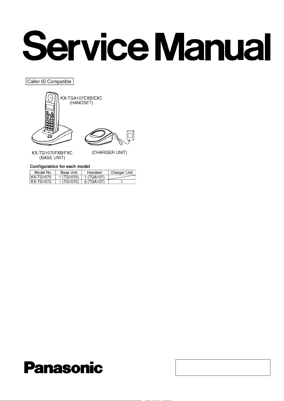
Panasonic KX-TG1070FXB, KX-TG1070FXC, KX-TG1072FXB, KX-TGA107EXB, KX-TGA107EXC Service manual
ORDER NO. KM40610223CE
Telephone Equipment
KX-TG1070FXB
KX-TG1070FXC
KX-TG1072FXB
KX-TGA107EXB
KX-TGA107EXC
Digital Cordless Phone
Black Version
Blue Version
(for Central Europe)
© 2006 Panasonic Communications Co., Ltd. All
rights reserved. Unauthorized copying and distribution is a violation of law.
KX-TG1070FXB/KX-TG1070FXC/KX-TG1072FXB/KX-TGA107EXB/KX-TGA107EXC
2

TABLE OF CONTENTS
PAG E
1 Safety Precaution ------------------------------------------------ 4
1.1. For Service Technicians --------------------------------- 4
2 Warning-------------------------------------------------------------- 4
2.1. Battery Caution--------------------------------------------- 4
2.2. About Lead Free Solder (Pbf: Pb free)--------------- 4
3 Specifications ----------------------------------------------------- 6
4 Technical Descriptions----------------------------------------- 7
4.1. Block Diagram (Base Unit)------------------------------ 7
4.2. Circuit Operation (Base Unit)--------------------------- 8
4.3. Block Diagram (Handset)-------------------------------- 9
4.4. Circuit Operation (Handset)----------------------------10
4.5. Signal Flow------------------------------------------------- 11
5 Location of Controls and Components ------------------12
5.1. Controls -----------------------------------------------------12
6 Installation Instructions---------------------------------------12
6.1. Connections------------------------------------------------12
6.2. Battery-------------------------------------------------------13
7 Operation Instructions-----------------------------------------14
7.1. Guide to Telephone Settings---------------------------14
7.2. Handset Registration ------------------------------------14
7.3. For Service Hint-------------------------------------------14
8 Service Mode -----------------------------------------------------15
8.1. Engineering Mode----------------------------------------15
8.2. How to Clear User Setting------------------------------19
8.3. How to Set When Replacing Unit---------------------20
9 Troubleshooting Guide----------------------------------------22
9.1. How to Replace the Flat Package IC ----------------23
10 Disassembly and Assembly Instructions ---------------25
10.1. Disassembly Instructions-------------------------------25
11 Schema t ic Di a gram ---------------------------------------------27
11.1. For Schematic Diagram---------------------------------27
11.2. Schematic Diagram (Base Unit_Main) --------------28
11.3. Schematic Diagram (Base Unit_Operation) -------31
11.4. Schematic Diagram (Handset) ------------------------32
12 Printed Circuit Board-------------------------------------------35
12.1. Circuit Board (Base Unit) -------------------------------35
12.2. Circuit Board (Base Unit_Page key) -----------------37
12.3. Circuit Board (Handset)---------------------------------39
13 Exploded View and Replacement Parts List -----------41
KX-TG1070FXB/KX-TG1070FXC/KX-TG1072FXB/KX-TGA107EXB/KX-TGA107EXC
3
KX-TG1070FXB/KX-TG1070FXC/KX-TG1072FXB/KX-TGA107EXB/KX-TGA107EXC
1 Safety Precautions
1.1. For Service Technicians
ICs and LSIs are vulnerable to static electricity.
When repairing, the following precautions will help prevent recurring malfunctions.
1. Cover the plastic parts boxes with aluminum foil and ground them.
2. Ground the soldering irons.
3. Use a conductive mat on the worktable.
4. Do not touch IC or LSI pins with bare fingers.
2Warning
2.1. Battery Caution
1. Danger of explosion if battery is incorrectly replaced.
2. Replace only with the same or equivalent type recommended by the manufacturer.
3. Dispose of used batteries according to the manufacture’s Instructions.
2.2. About Lead Free Solder (Pbf: Pb free)
Note:
In the information below, Pb, the symbol for lead in the periodic table of elements, will refer to standard solder or solder that contains lead.
We will use PbF solder when discussing the lead free solder used in our manufacturing process which is made from Tin (Sn),
Silver (Ag), and Copper (Cu).
This model, and others like it, manufactured using lead free solder will have PbF stamped on the PCB. For service and repair
work we suggest using the same type of solder.
Caution
• PbF solder has a melting point that is 50 °F ~ 70 °F (30 °C ~ 40 °C) higher than Pb solder. Please use a soldering iron with
temperature control and adjust it to 700 °F ± 20 °F (370 °C ± 10 °C).
• Exercise care while using higher temperature soldering irons.:
Do not heat the PCB for too long time in order to prevent solder splash or damage to the PCB.
• PbF solder will tend to splash if it is heated much higher than its melting point, approximately 1100 °F (600 °C).
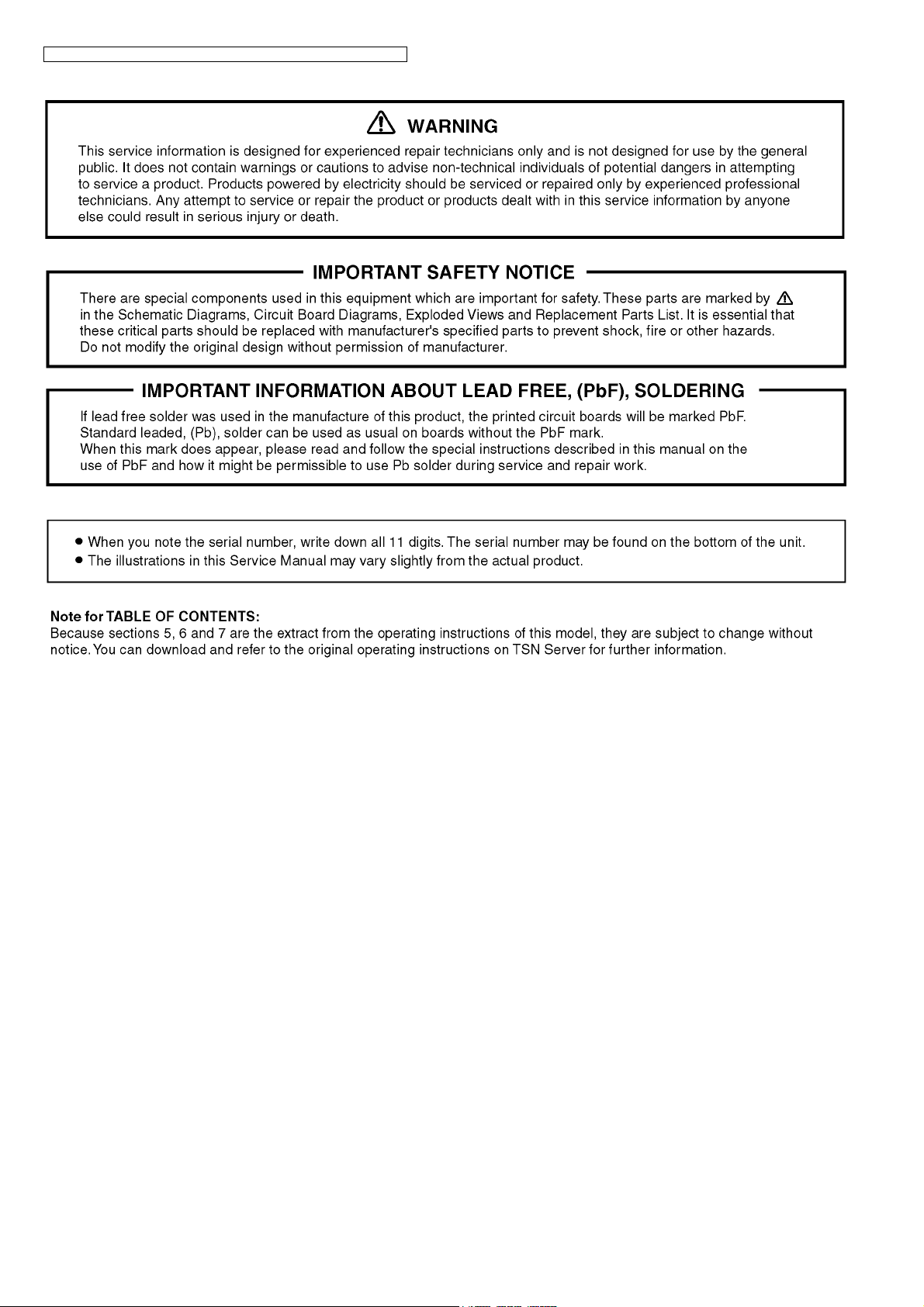
• When applying PbF solder to double layered boards, please check the component side for excess which may flow onto the
opposite side (See the figure below).
4
KX-TG1070FXB/KX-TG1070FXC/KX-TG1072FXB/KX-TGA107EXB/KX-TGA107EXC
d
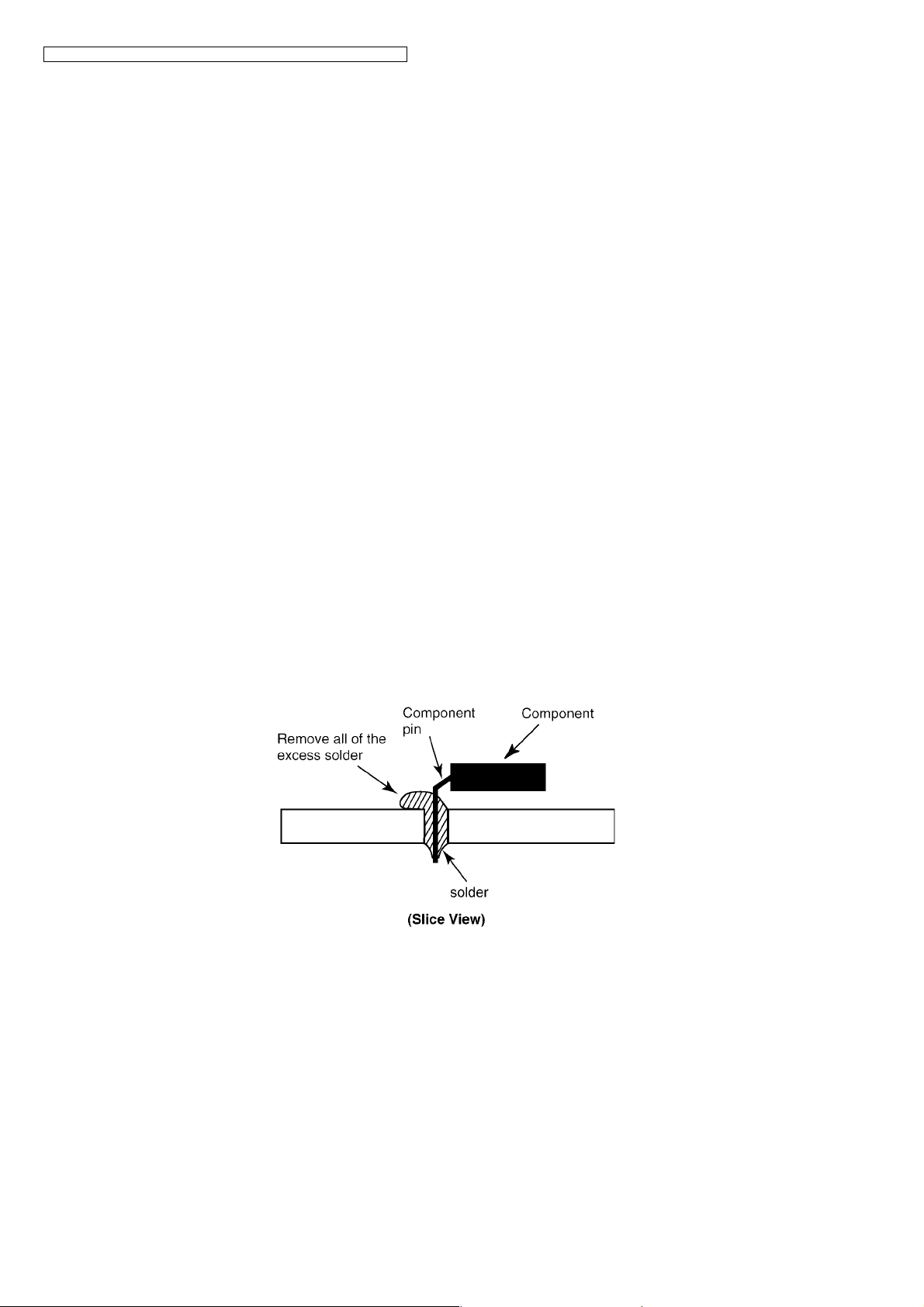
2.2.1. Suggested PbF Solder
There are several types of PbF solder available commercially. While this product is manufactured using Tin, Silver, and Copper
(Sn+Ag+Cu), you can also use Tin and Copper (Sn+Cu) or Tin, Zinc, and Bismuth (Sn+Zn+Bi). Please check the manufacturer’s
specific instructions for the melting points of their products and any precautions for using their product with other materials.
The following lead free (PbF) solder wire sizes are recommended for service of this product: 0.3 mm, 0.6 mm and 1.0 mm.
2.2.2. How to Recognize that Pb Free Solder is Used
(Example: Handset P.C.B.)
Marke
> EP-GW <
35-006057-005-200
RF
U4
U3
(Component View)
Note:
The location of the “PbF” mark is subject to change without notice.
PbF
5
KX-TG1070FXB/KX-TG1070FXC/KX-TG1072FXB/KX-TGA107EXB/KX-TGA107EXC
3 Specifications
Note:
• Specifications are subject to change.
Connections:
The unit will not work during a power failure. We recommend you connect a standard telephone on the same line for power protection.
Note for Service:
• Operation range: Up to 300 m outdoors, Up to 50 m indoors, depending on the condition.
• Analog telephone connection: Telephone Line
6
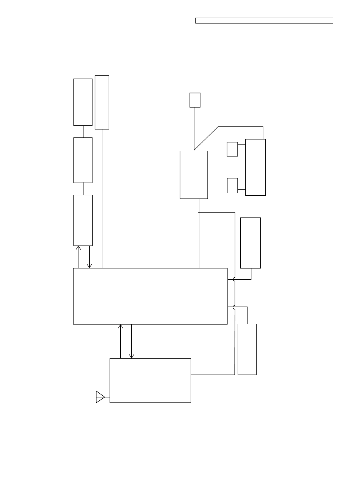
4 Technical Descriptions
4.1. Block Diagram (Base Unit)
Tel Line
Locator button
Interface
TEL Line
D1~ D4, Q7
KX-TG1070FXB/KX-TG1070FXC/KX-TG1072FXB/KX-TGA107EXB/KX-TGA107EXC
DC6V
Power
DC
6V
U1
Linear
Regulator
Charge Contact
Limiter
Current
KX-TG1070/1072 BLOCK DIAGRAM (BASE UNIT)
Speech
Q605
37
Network
32
64
Base
Band
Controller
ANT
U2
14
R -D ATA
6
15
T- DATA
4
RF Module
3.3V
2, 52
3.3V
17, 18 50, 51
U3
EEPROM
Crystal
13.824MHz
7

KX-TG1070FXB/KX-TG1070FXC/KX-TG1072FXB/KX-TGA107EXB/KX-TGA107EXC
4.2. Circuit Operation (Base Unit)
The base-station consists of base band controller, speech network, tel-line interface, RF module, linear regulator, EEPROM,
crystal and so on. Refer to Block Diagram (Base Unit) (P.7).
4.2.1. Base Band Controller
These are parts to control all function of the base-station, we used the Philips XS which is controller for DECT. These devices
include all control circuits of the base-station for RF module, tel-line interface, ADPCM codec, series regulator and so on.
4.2.2. Power Supply
The power supply consists with CM1117 voltage regulator ICs.
CM1117 generate DC 3.3V voltage from DC 6V voltage from adaptor. DC 3.3V are used for RF module & I/O port, DC 2.5V &
DC1.8V are used for the base band controller and the circumference circuits.
4.2.3. Speech Network
The TR circuit is used for speech network. The function of this connects tel-line interface and the base band controller.
4.2.4. TEL Line Interface
The function of this connects tel-line and speech network. Also, the tel-line interface include the ring detect circuit, caller-ID circuit.
4.2.5. EEPROM
This is 8K bits memory. The each kind of value to set-up at power-on, redial memory, speed-dialing memory, and so on are
stored in this device.
4.2.6. RF Module
Receiver part: RF signals induced at the antenna are extracted by the RF control interface. The RF signal to be selected is
demodulated into RX_DATA signals. And signals is passed to the base band controller.
Transmitter part: The signal from transceiver chip-set is fed to the antenna through the RF power amplifier by control of the RF
control interface. And then this signal is radiated from antenna.
Logical part: The frequency to be used is generated in transceiver chip-set by control signals (CLK, DATA, ENABLE, SYRI) of
the RF control interface.
4.2.7. Current Limiter
The current limiter is circuit to supply the proper current to charge batteries of the handset from DC 6V voltage.
8
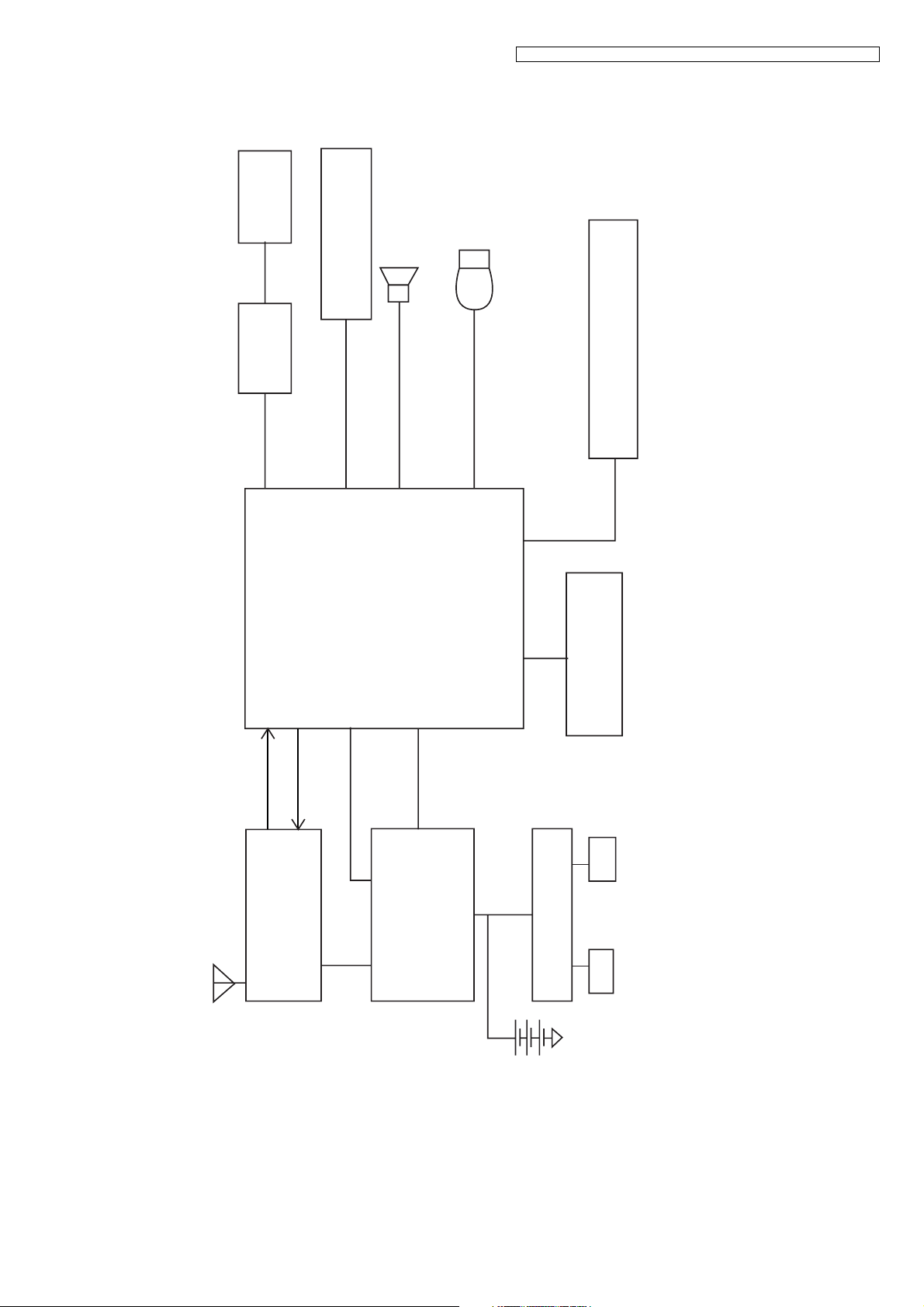
4.3. Block Diagram (Handset)
LCD
KEYPAD
KX-TG1070FXB/KX-TG1070FXC/KX-TG1072FXB/KX-TGA107EXB/KX-TGA107EXC
MIC
Ear Piece
U2
LCD Driver
54, 55, 56
14
15
57~62, 64, 1
U4
Controller
Base Band
2
32, 33
52
29, 30
50, 51
16, 17
U3
EEPROM
Crystal
13.824MHz
KX-TGA107 BLOCK DIAGRAM (HANDSET)
R-DATA
6
Antenna
T-DATA
4
RF Module
Switching
2.4V, 2-cell
Regulator
Q10
Charger
Charger Contact
Battery
9

KX-TG1070FXB/KX-TG1070FXC/KX-TG1072FXB/KX-TGA107EXB/KX-TGA107EXC
4.4. Circuit Operation (Handset)
The handset consists of Base Band Controller, LCD, RF module, keypad, regulator, charger, EEPROM, crystal, earpiece, ringer
& microphone, and so on.
4.4.1. Base Band Controller
The base band controller controls all function of the handset, Philips XS for the base band controller is used.
This device include all control circuits of the handset for RF module, LCD controller, keypad interface, earpiece, microphone,
ADPCM codec, switching and series regulator and so on.
4.4.2. Charger
The base-station supply DC 6V power to the charger and the charger charges the batteries to use this power. The signal on the
charger circuit is generated when the handset is to being charged this signal is used to control the charger circuit and for auto-
matic off-hook by cradle-off when an incoming call is coming.
4.4.3. 2.4V 2 cell & 3.3V output from internal switching regulator
The battery is (2.4V / 2cell) directly supplied to switching regulator which controlling by base band controller and step up the DC
3.3V to the RF module & I/O port. DC 2.5V & DC1.8V are used for the base band and the circumference circuits.
4.4.4. RF Module
Receiver part: RF signals induced at the antenna are extracted by the RF control interface. The RF signal to be selected is
demodulated into RX_DATA signals. And signals is passed to the base band controller.
Transmitter part: The signal from transceiver chip-set is fed to the antenna through the RF power amplifier by control of the RF
control interface. And then this signal is radiated from antenna.
Logical part: The frequency to be used is generated in transceiver chip-set by control signals (CLK, DATA, ENABLE, SYRI) of
the RF control interface.
4.4.5. LCD
The LCD consists of 7-segment, 12 digit display and 13 icon which controlling by the LCD display driver.
4.4.6. Keypad
The keypad consists of 12 dialing keys and 8 function keys.
10

KX-TG1070FXB/KX-TG1070FXC/KX-TG1072FXB/KX-TGA107EXB/KX-TGA107EXC
4.5. Signal Flow
4.5.1. Talk mode:
Rx audio signal from line interface at “LINERX_P” path into B/S MCU (pin 32, 33) and then signal from B/S RF transform, H/S RF
receive signal forward to MCU, H/S MCU from (pin 32, 33) receive path output audio signal to receiver.
Tx audio signal from MIC receive audio signal at mic path into H/S MCU and then audio signal from H/S RF transform, B/S RF
receive signal forward to MCU, B/S MCU audio signal from (Pin 30, 29) at “LINETX_P” path transmit to line interface out of PSTN.
4.5.2. Ringer detect:
Telephone line have ringer signal from tip ring into Base, and then Base transistor Q8 turn on and ringer data signal for Base MCU
(Pin 58_IOGP16) detect and the handset buzzer have product “Melody tone”.
4.5.3. Type I CID receive:
CID signal from tip ring couple CID signal at (CID1_P, CID1_N) path into Base MCU (Pin 29, 30) detect, Handset display show the
telephone no.
11
KX-TG1070FXB/KX-TG1070FXC/KX-TG1072FXB/KX-TGA107EXB/KX-TGA107EXC
5 Location of Controls and
Components
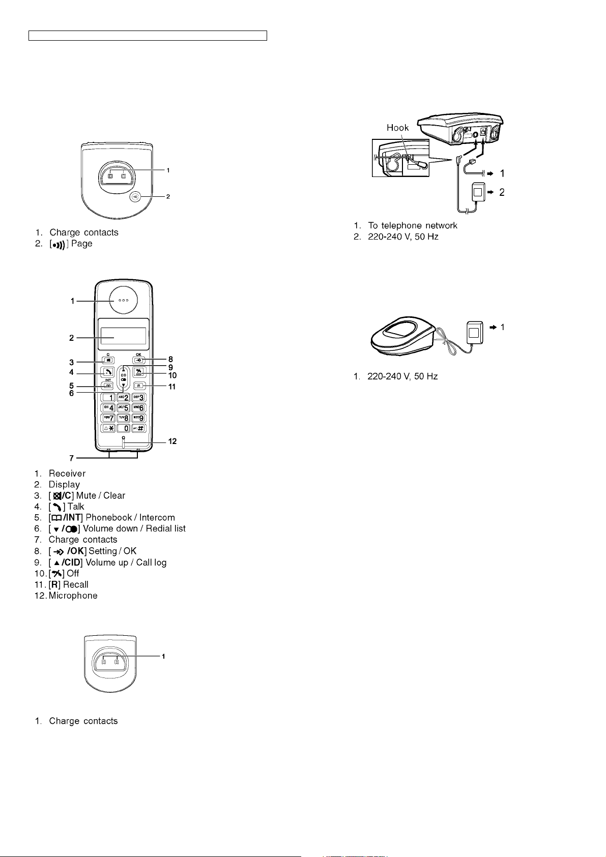
5.1. Controls
5.1.1. Base Unit
5.1.2. Handset
6 Installation Instructions
6.1. Connections
Base Unit
Note:
• Use only the included AC adaptor and telephone line cord.
• Connect the AC adaptor securely to the AC outlet.
Charger
5.1.3. Charger
Note:
• Never install telephone wiring during a lightning storm.
• Do not connect the AC adaptor to a ceiling-mounted AC outlet, as the weight of the adaptor may cause it to become disconnected.
Location
• For maximum distance and noise-free operation, place your
base unit:
- Away from electrical appliances such as TVs, radios,
personal computers or other phones.
- In a convenient, high and central location.
12
KX-TG1070FXB/KX-TG1070FXC/KX-TG1072FXB/KX-TGA107EXB/KX-TGA107EXC
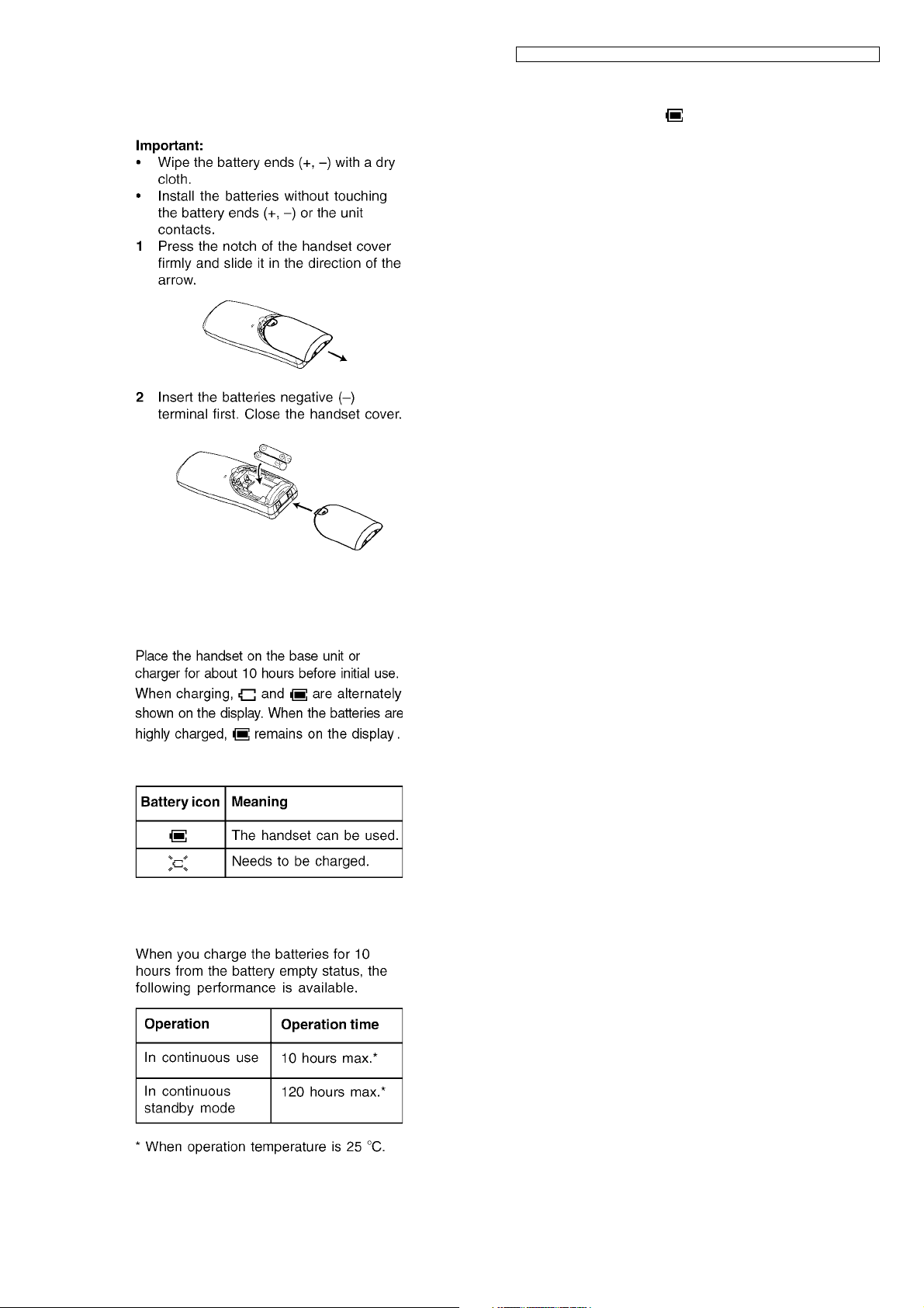
6.2. Battery
6.2.1. Battery Installation
Note:
• It takes 10 hours to fully charge the batteries, however, you
can use the handset if remains on the display while
charging.
• It is normal for batteries not to reach full capacity at the initial
charge. Maximum battery performance is reached after a
few complete cycles of charge/discharge (use).
• Actual battery performance depends on a combination of
how often the handset is in use and how often it is not in use
(standby).
• Even after the handset is fully charged, the handset can be
left on the base unit or charger without any ill effect on the
batteries.
• The battery strength may not be displayed correctly after you
replace the batteries. In this case, place the handset on the
base unit or charger and charge for at least 10 hours.
Note:
• Use only the included rechargeable batteries HHR-55AAAB
or HHR-4EPT.
6.2.2. Battery Charge
6.2.3. Battery Strength
6.2.4. Panasonic Ni-MH Battery
Performance
13
 Loading...