

Page 1
ORDER NO. KM40308180C3
Telephone Equipment
KX-TC2000NZB
KX-TC2000NZW
KX-TC2000NZF
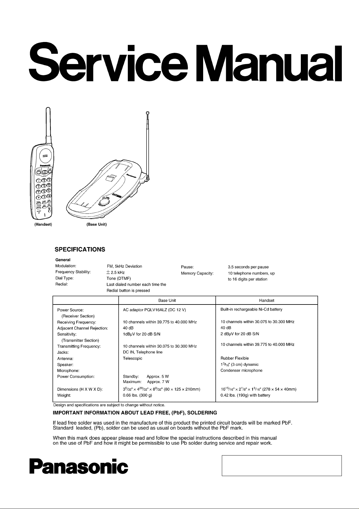
Cordless Phone
Black Version
White Version
Blue Version
(for New Zealand)
© 2003 Panasonic Communications Co., Ltd. All
rights reserved. Unauthorized copying and
distribution is a violation of law.
Page 2
KX-TC2000NZB / KX-TC2000NZW / KX-TC2000NZF
CONTENTS
Page Page
1 ABOUT LEAD FREE SOLDER (PbF: Pb free) 4
1.1. Suggested PbF Solder
1.2. How to recognize that Pb Free solder is used
2 FOR SERVICE TECHNICIANS
3 CAUTION
4 BATTERY
4.1. Recharge
4.2. Battery information
5 BATTERY REPLACEMENT
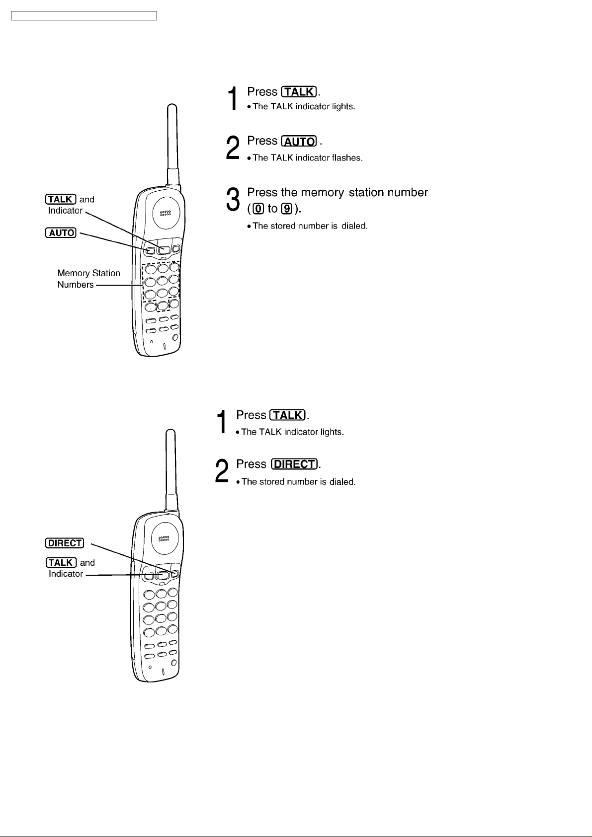
6 LOCATION OF CONTROLS
6.1. Base Unit
6.2. Handset
7 CONNECTION
8 OPERATIONS
8.1. Making Calls
8.2. Answering Calls
8.3. Storing Phone Numbers in Memory
8.4. Storing a Phone Number in the DIRECT Button
8.5. Dialing a Stored Number
8.6. Dialing the Stored Number in the DIRECT Button
8.7. Recall Button
9 DISASSEMBLY INSTRUCTIONS
10 TR OUBLESHOOTING GUIDE
10.1. Check Power
10.2. Bell Reception
10.3. Check Battery Charge
10
12
12
12
13
13
14
14
15
16
18
19
20
21
4
5
6
6
7
7
7
8
9
9
9
10.4. Check Link
10.5. Check Handset Transmission
10.6. Check Handset Reception
11 ADJUSTMENTS (BASE UNIT)
11.1. Test Mode Flow Chart (Base Unit)
11.2. How to change the channel
11.3. Adjustment
11.4. Adjustment Standard (Base Unit)
12 ADJUSTMENTS (HANDSET)
12.1. Test Mode Flow Chart (Handset)
12.2. How to change the channel
12.3. Adjustment
12.4. Adjustment Standard (Handset)
13 R F SPECIFICAT ION
13.1. Base Unit
13.2. Handset
14 HOW TO CHECK THE HANDSET SPEAKER
15 FREQUENCY TABLE (MHz)
16 EXPLANATION OF CPU DATA COMMUNICATION
16.1. STAND-BY -> TALK, TALK -> STAND-BY
16.2. Ringing
16.3. Changing the Channel
16.4. Ports for transmitting and receiving of data
16.5. Waveform of DATA used for cordless transmission and
reception
17 B LOCK DIAGRAM (BASE UNIT)
22
24
24
25
25
26
26
27
28
28
29
29
30
32
32
32
32
33
34
34
35
36
37
37
38
2
Page 3
KX-TC2000NZB / KX-TC2000NZW / KX-TC2000NZF
18 B LOCK DIAGRAM (HANDSET) 39
19 CIRCUIT OPERATION
19.1. Outline
19.2. Power Supply Circuit
19.3. Reset Circuit (Base Unit)
19.4. Charge Circuit
19.5. Telephone Line Interface
19.6. DTMF
19.7. Transmitter/Receiver
19.8. Signal Route
20 CIRCUIT OPERATION (HANDSET)
20.1. Reset Circuit (Handset)
20.2. Battery Low / Power Down Detector
21 CPU DATA (Base Unit)
21.1. IC2
22 CPU DATA (Handset)
22.1. IC2
23 RF IC (Base Unit and Handset)
23.1. IC1
24 HOW TO REPLACE FLAT PACKAGE IC
24.1. Preparation
24.2. Procedure
24.3. Modification Procedure of Bridge
40
40
41
42
43
43
43
44
46
47
47
48
49
49
50
50
51
51
52
52
52
52
25 C ABINET AND ELECTRICAL PARTS LOCATION (BASE UN IT)
26 C ABINET AND ELECTRICAL PARTS LOCATION (HANDET)
27 ACCESSORIES AND PACKING MATERIALS
28 REPLACEMENT PARTS LIST
28.1. Base Unit
28.2. Handset
28.3. ACCESSORIES AND PACKING MATERIALS
29 FOR SCHEMATIC DIAGRAM
29.1. Base Unit (SCHEMATIC DIAGRAM (Base Unit))
29.2. Handset (SCHEMATIC DIAGRAM (Handset))
30 SCHEMATIC DIAGRAM (Base Unit)
30.1. Base Unit
30.2. RF Unit (Base Unit)
31 SCHEMATIC DIAGRAM (Handset)
31.1. Handset
31.2. RF Unit (Handset)
31.3. Memo
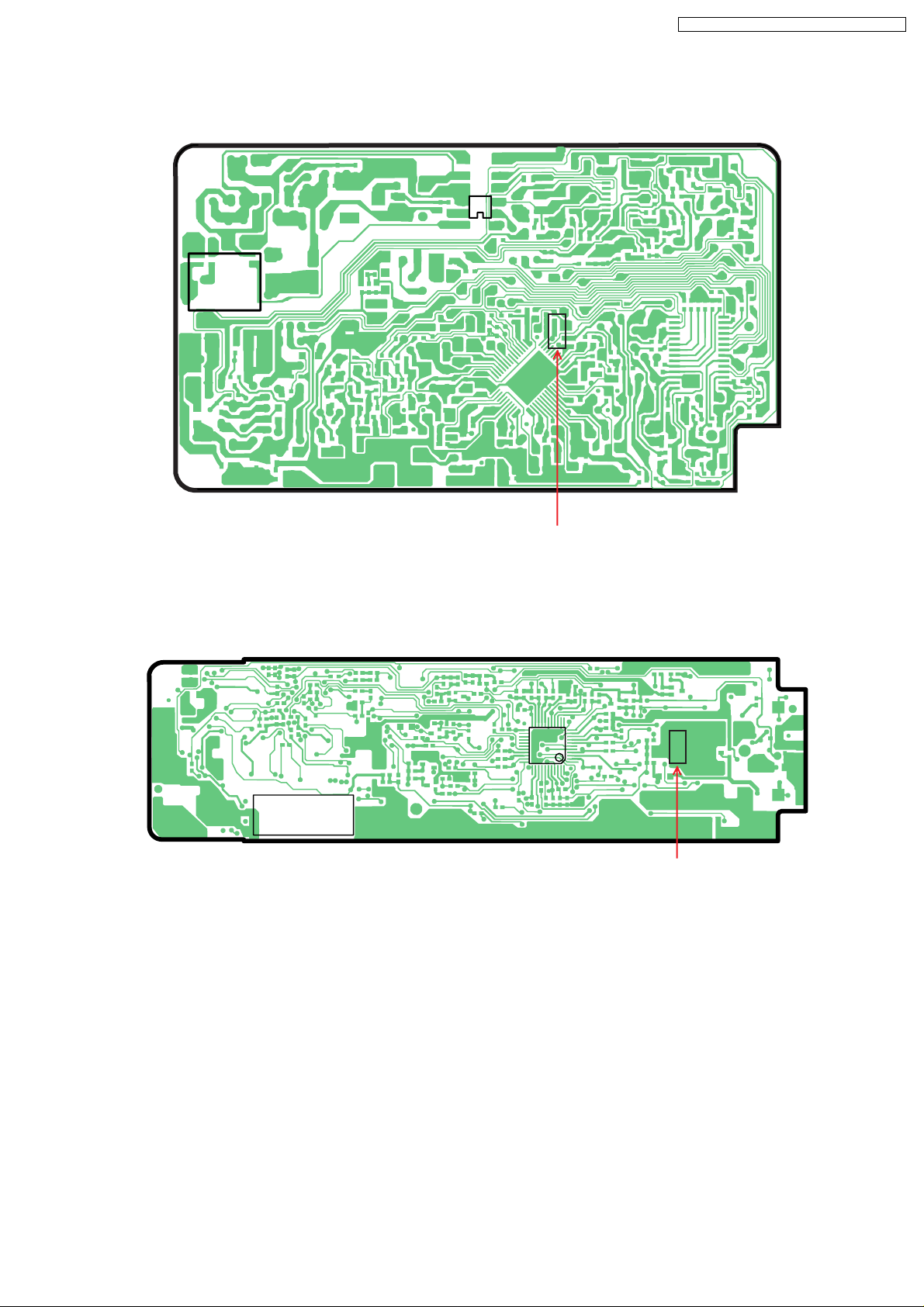
32 CIRCUIT BOARD (Base Unit)
32.1. Component View
32.2. Flow Solder Side View
33 CIRCUIT BOARD (Handset)
33.1. Component View
33.2. Flow Solder Side View
53
54
55
56
56
58
60
61
61
61
62
62
63
64
64
65
66
67
67
68
69
69
70
3
Page 4
KX-TC2000NZB / KX-TC2000NZW / KX-TC2000NZF
1 ABOUT LEAD FREE SOLDER (PbF: Pb free)
Note:
In the information below, Pb, the symbol for lead in the periodic table of elements, will refer to standard solder or solder that
contains lead.
We will use PbF solder when discussing the lead free solder used in our manufacturing process which is made from Tin (Sn),
Silver (Ag), and Copper (Cu).
This model, and others like it, manufactured using lead free solder will have PbF stamped on the PCB. For service and repair
work we suggest using the same type of solder although, with some precautions, standard Pb solder can also be used.
Caution
•
• PbF solder has a melting point that is 50°F ~ 70° F (30°C ~ 40°C) higher than Pb solder. Please use a soldering iron with
• •
temperature control and adjust it to 700°F ± 50° F (370°C ± 10°C). In case of using high temperature soldering iron, please
be careful not to heat too long.
•
• PbF solder will tend to splash if it is heated much higher than its melting point, approximately 1100°F (600°C).
• •
•
• If you must use Pb solder on a PCB manufactured using PbF solder, remove as much of the original PbF solder as possible
• •
and be sure that any remaining is melted prior to applying the Pb solder.
•
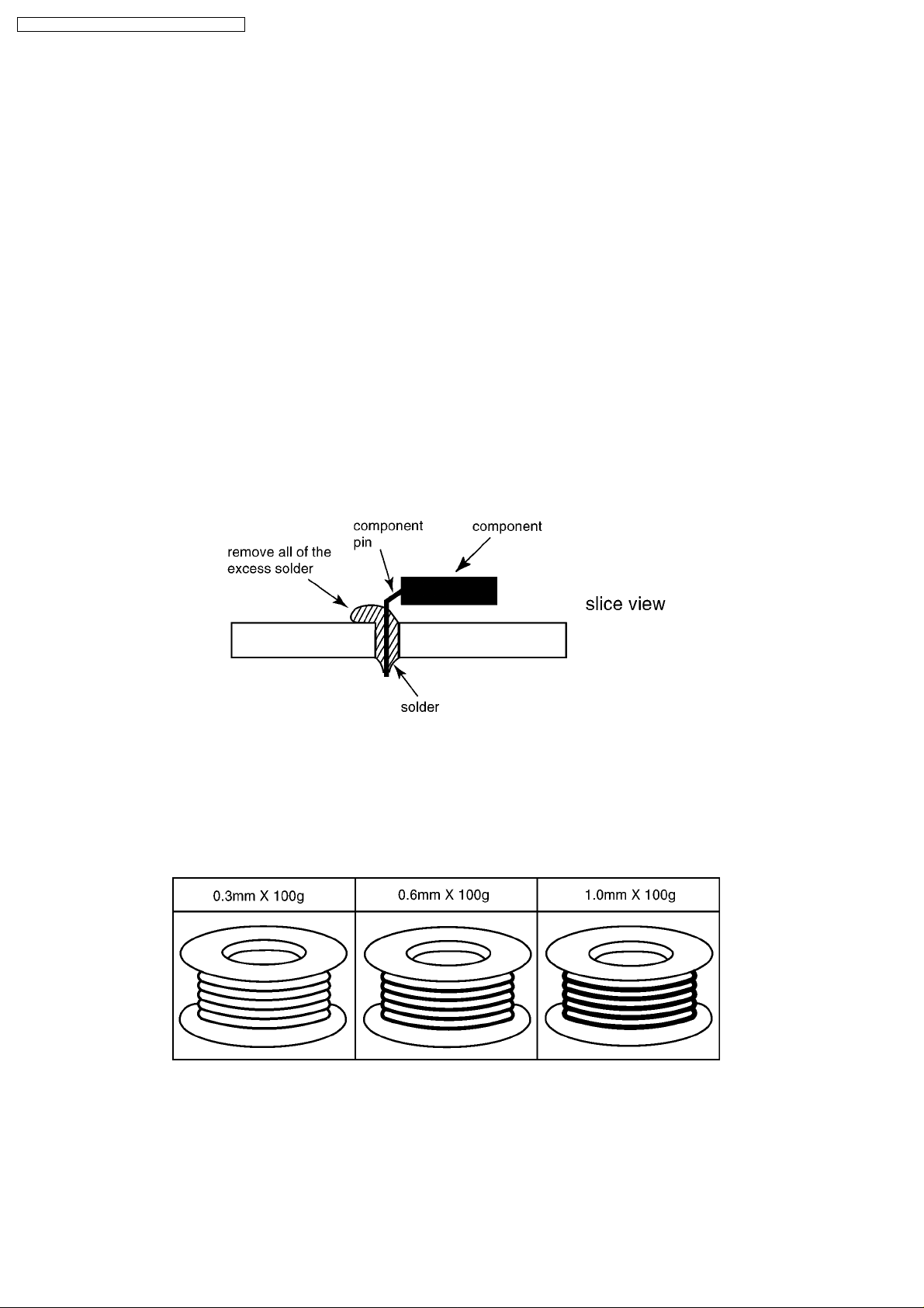
• When applying PbF solder to double layered boards, please check the component side for excess which may flow onto the
• •
opposite side (See the figure below).
1.1. Suggested PbF Solder
There are several types of PbF solder available commercially. While this product is manufactured using Tin, Silver, and Copper
(Sn+Ag+Cu), you can also use Tin and Copper (Sn+Cu), or Tin, Zinc, and Bismuth (Sn+Zn+Bi). Please check the manufac
turer’s specific instructions for the melting points of their products and any precautions for using their product with other
materials.
The following lead free (PbF) solder wire sizes are recommended for service of this product: 0.3mm, 0.6mm and 1.0mm.
4
Page 5
1.2. How to recognize that Pb Free solder is used
1.2.1. Base Unit Main PCB
IC5
JK1
PbF
KX-TC2000NZB / KX-TC2000NZW / KX-TC2000NZF
(Component View)
Note:
The location of the "PbF" marks is subject to change without notice.
1.2.2. Handset PCB
DPX1
(Component View)
Note:
The location of the "PbF" marks is subject to change without notice.
Marked
IC2
PbF
Marked
5
Page 6

KX-TC2000NZB / KX-TC2000NZW / KX-TC2000NZF
2 FOR SERVICE TECHNICIANS
ICs and LSIs are vulnerable to static electricity.
When repairing, the following precautions will help prevent recurring malfunctions.
1. Cover plastic parts boxes with aluminum foil.
2. Ground the soldering irons.
3. Use a conductive mat on worktable.
4. Do not grasp IC or LSI pins with bare fingers.
3 CAUTION
Danger of explosion if battery is incorrectly replaced.
Replace only with the same or equivalent type recommended by the manufacturer.
Dispose of used batteries according to the manufacturer´s Instructions.
6
Page 7
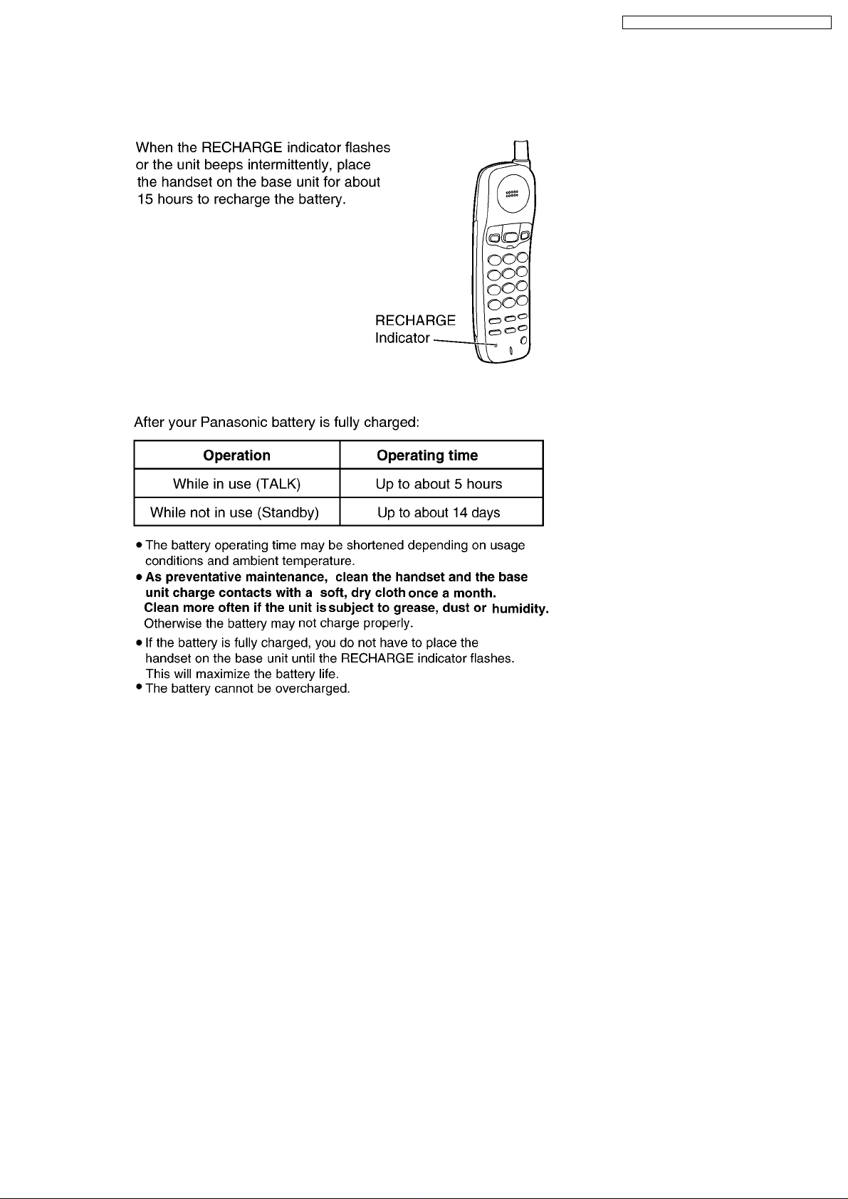
4 BATTERY
4.1. Recharge
4.2. Battery information
KX-TC2000NZB / KX-TC2000NZW / KX-TC2000NZF
7
Page 8
KX-TC2000NZB / KX-TC2000NZW / KX-TC2000NZF
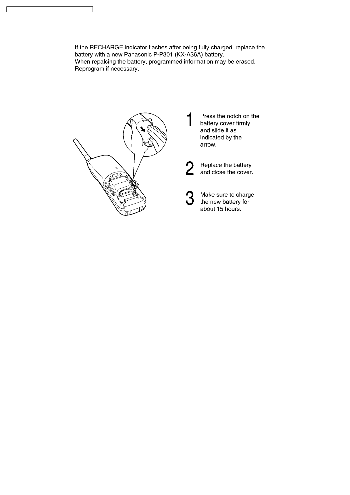
5 BATTERY REPLACEMENT
8
Page 9
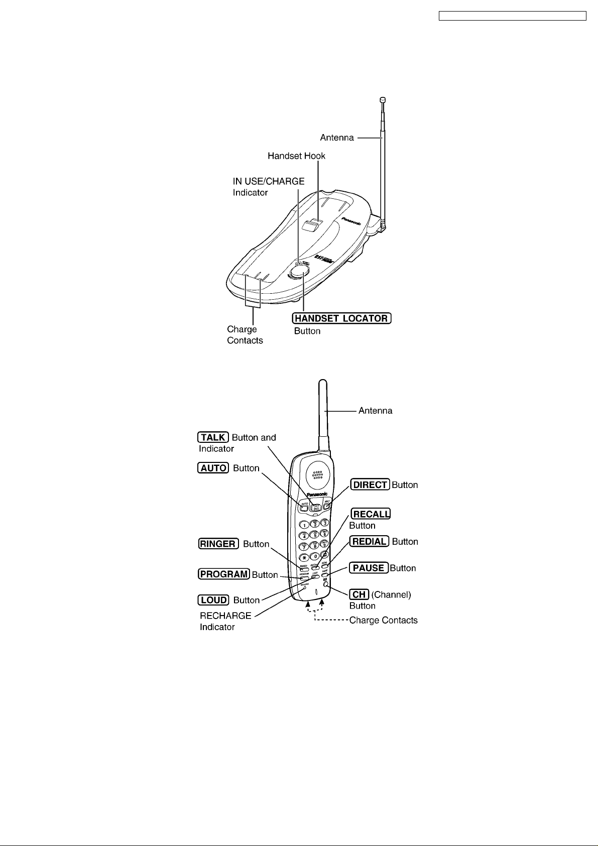
6 LOCATION OF CONTROLS
6.1. Base Unit
KX-TC2000NZB / KX-TC2000NZW / KX-TC2000NZF
6.2. Handset
9
Page 10
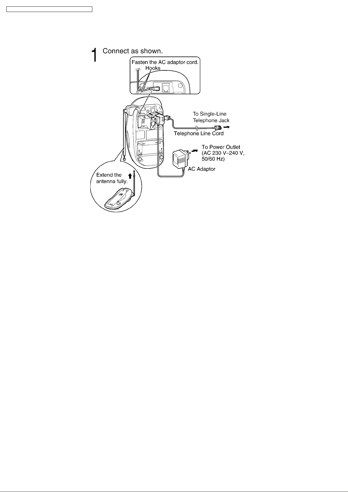
KX-TC2000NZB / KX-TC2000NZW / KX-TC2000NZF
7 CONNECTION
•
• USE ONLY WITH Panasonic AC ADAPTOR PQLV16AL.
• •
•
• The AC adaptor must remain connected at all times.
• •
(It is normal for the adaptor to feel warm during use.)
•
• This unit will not function during a power failure.
• •
If you want to connect a standard telephone on the same line, use a T-adaptor.
•
• KX-TC2000NZ is not designed to be used with rotary (pulse dialling) services.
• •
10
Page 11
For Service Hint:
KX-TC2000NZB / KX-TC2000NZW / KX-TC2000NZF
11
Page 12
KX-TC2000NZB / KX-TC2000NZW / KX-TC2000NZF
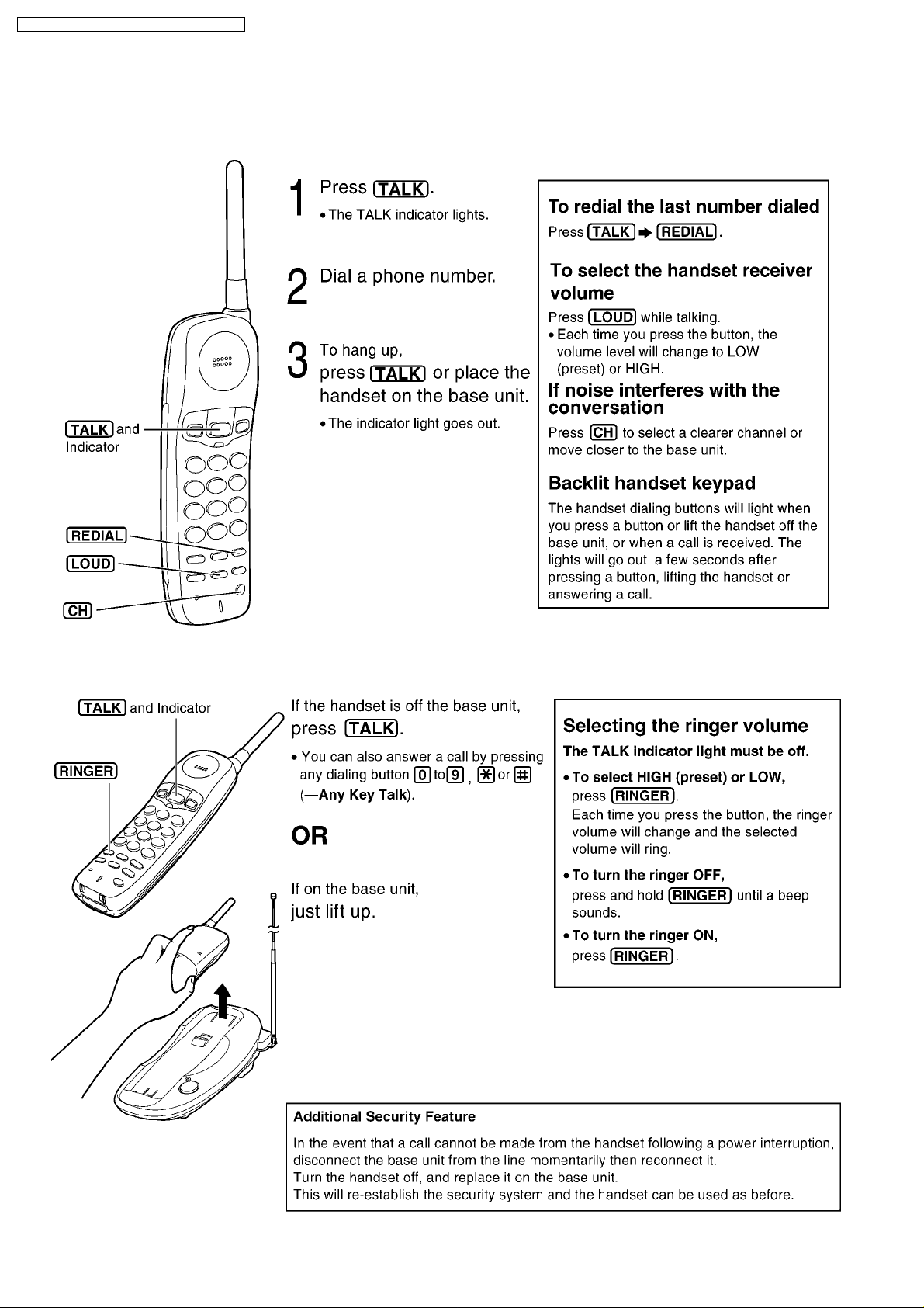
8 OPERATIONS
8.1. Making Calls
8.2. Answering Calls
12
Page 13
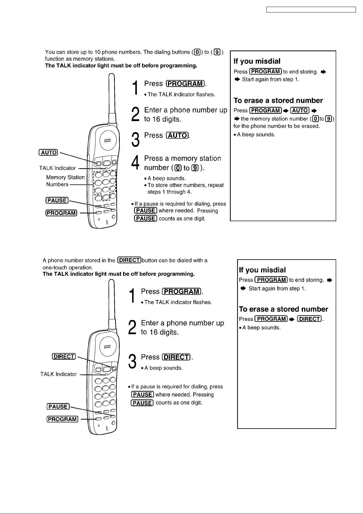
8.3. Storing Phone Numbers in Memory
KX-TC2000NZB / KX-TC2000NZW / KX-TC2000NZF
8.4. Storing a Phone Number in the DIRECT Button
13
Page 14
KX-TC2000NZB / KX-TC2000NZW / KX-TC2000NZF
8.5. Dialing a Stored Number
8.6. Dialing the Stored Number in the DIRECT Button
14
Page 15
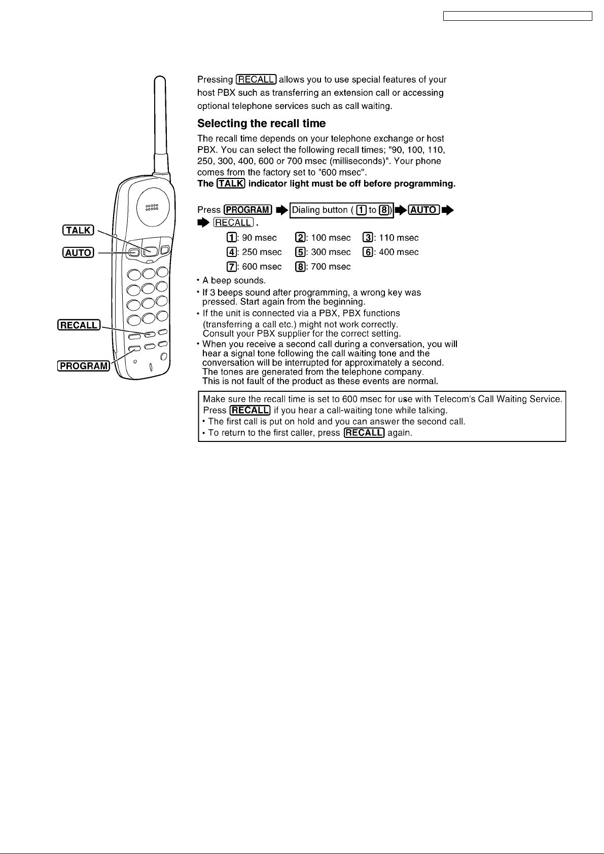
8.7. Recall Button
KX-TC2000NZB / KX-TC2000NZW / KX-TC2000NZF
15
Page 16

KX-TC2000NZB / KX-TC2000NZW / KX-TC2000NZF
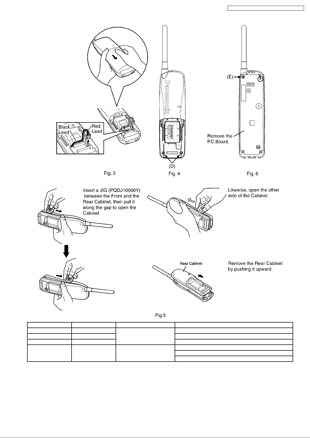
9 DISASSEMBLY INSTRUCTIONS
Show in Fig. Procedure To remove. Remove.
1 1 Lower Cabinet Screws (2.6 × 12)....................... (A) × 4
2 1, 2 Main P.C. Board Screw (2.6 × 6).......................... (B) × 1
Screw (2.6 × 12).......................... (C) × 1
Solder
Main P.C. Board.
16
Page 17
KX-TC2000NZB / KX-TC2000NZW / KX-TC2000NZF
Show in Fig. Procedure To remove. Remove.
3 3 Rear Cabinet Battery compartment cover.
4 3, 4 Screws (2.6 × 12)......................(D) × 2
5 3, 4, 5 Follow the procedure.
6 3, 4, 5, 6 Main P. C. Board Screw (2.6 × 12)........................(E) × 1
Tape and solder.
Main P. C. Board.
17
Page 18
KX-TC200 0NZB / KX-TC2000NZW / KX-TC200 0NZ F
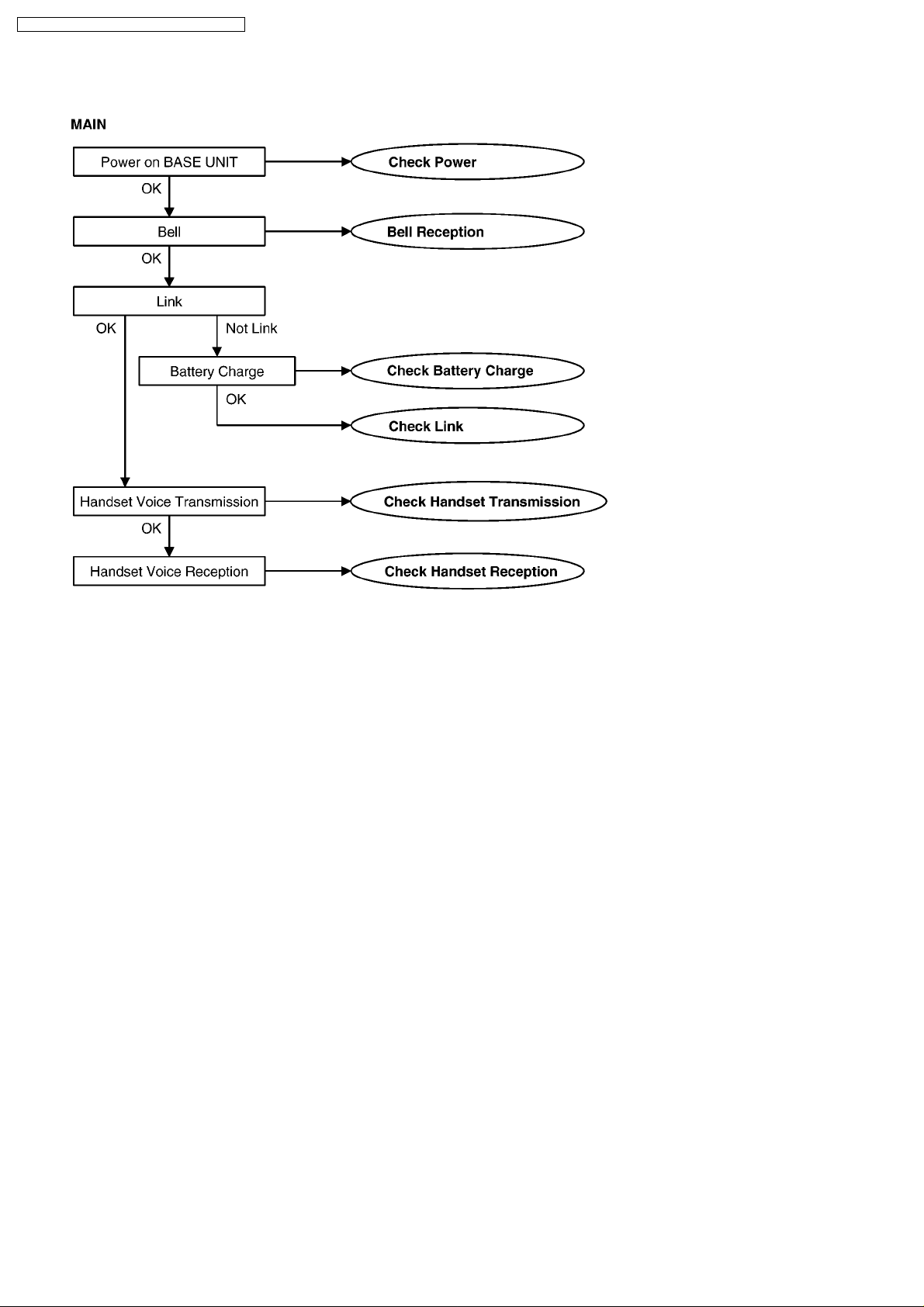
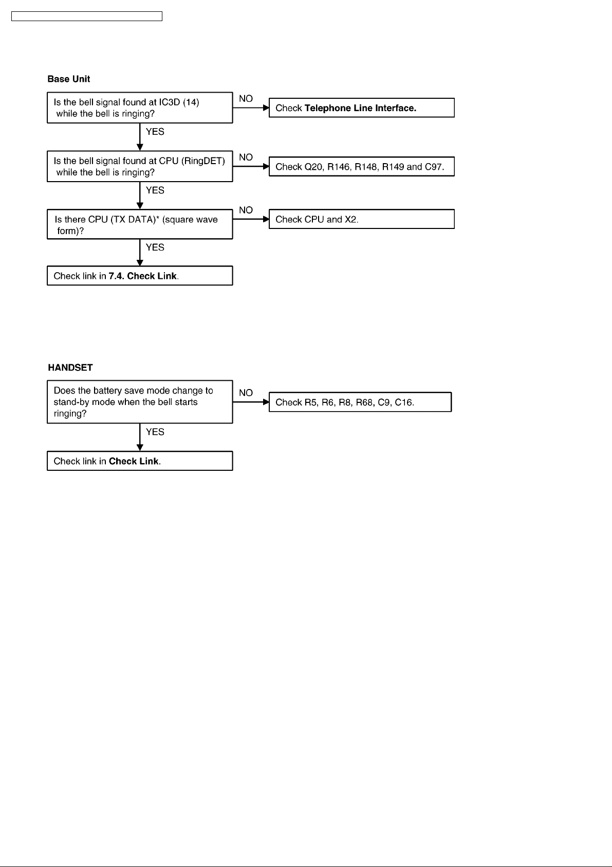
10 TROUBLESHOOTING GUIDE
Cross Reference:
Check Power (P.19)
Bell Reception (P.20)
Check Battery Char ge (P.21)
Check Link (P.22)
Check Handset Transmission (P.24)
Check Handset Reception (P.24)
18
Page 19

10.1. Check Power
KX-TC2000NZB / KX-TC2000NZW / KX-TC2000NZF
Cross Reference:
Reset Circuit (Base Unit) (P.42)
Power Supply Circuit (P.41)
Cross Reference:
Charge Circuit (P.43)
*: Each measurement points are shown in CIRCUIT BOARD (Base Unit) (P.67) or CIRCUIT BOARD (Handset) (P.69)
Note:
CPU: IC2
Note:
CPU: IC2
19
Page 20
KX-TC2000NZB / KX-TC2000NZW / KX-TC2000NZF
10.2. Bell Reception
Cross Reference:
Check Link (P.22)
Telephone Line Interface (P.43)
Cross Reference:
Check Link (P.22)
*: Each measurement points are shown in CIRCUIT BOARD (Base Unit) (P.67) or CIRCUIT BOARD (Handset) (P.69)
Note:
CPU: IC2
20
Page 21
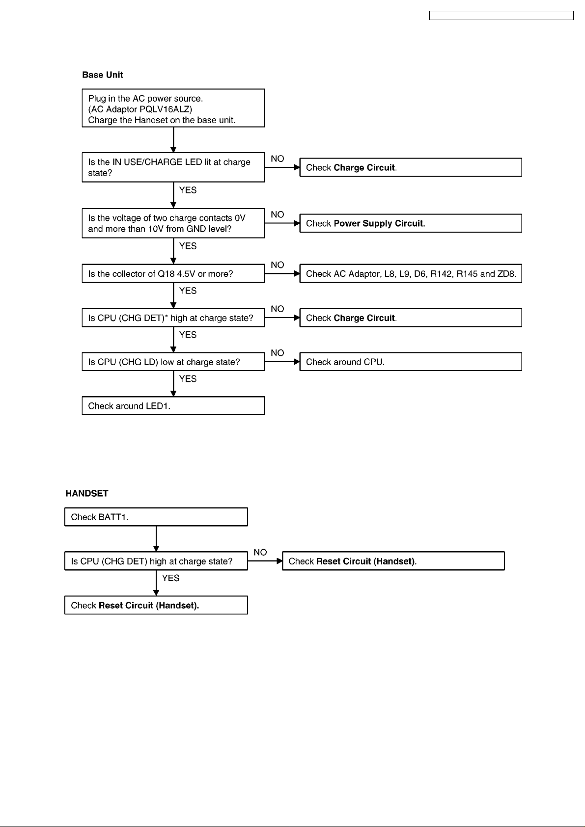
10.3. Check Battery Charge
KX-TC2000NZB / KX-TC2000NZW / KX-TC2000NZF
Cross Reference:
Charge Circuit (P.43)
Power Supply Circuit (P.41)
Cross Reference:
Reset Circuit (Handset) (P.47)
*: Each measurement points are shown in CIRCUIT BOARD (Base Unit) (P.67) or CIRCUIT BOARD (Handset) (P.69)
Note:
CPU: IC2
Note:
CPU: IC2
21
Page 22
KX-TC2000NZB / KX-TC2000NZW / KX-TC2000NZF
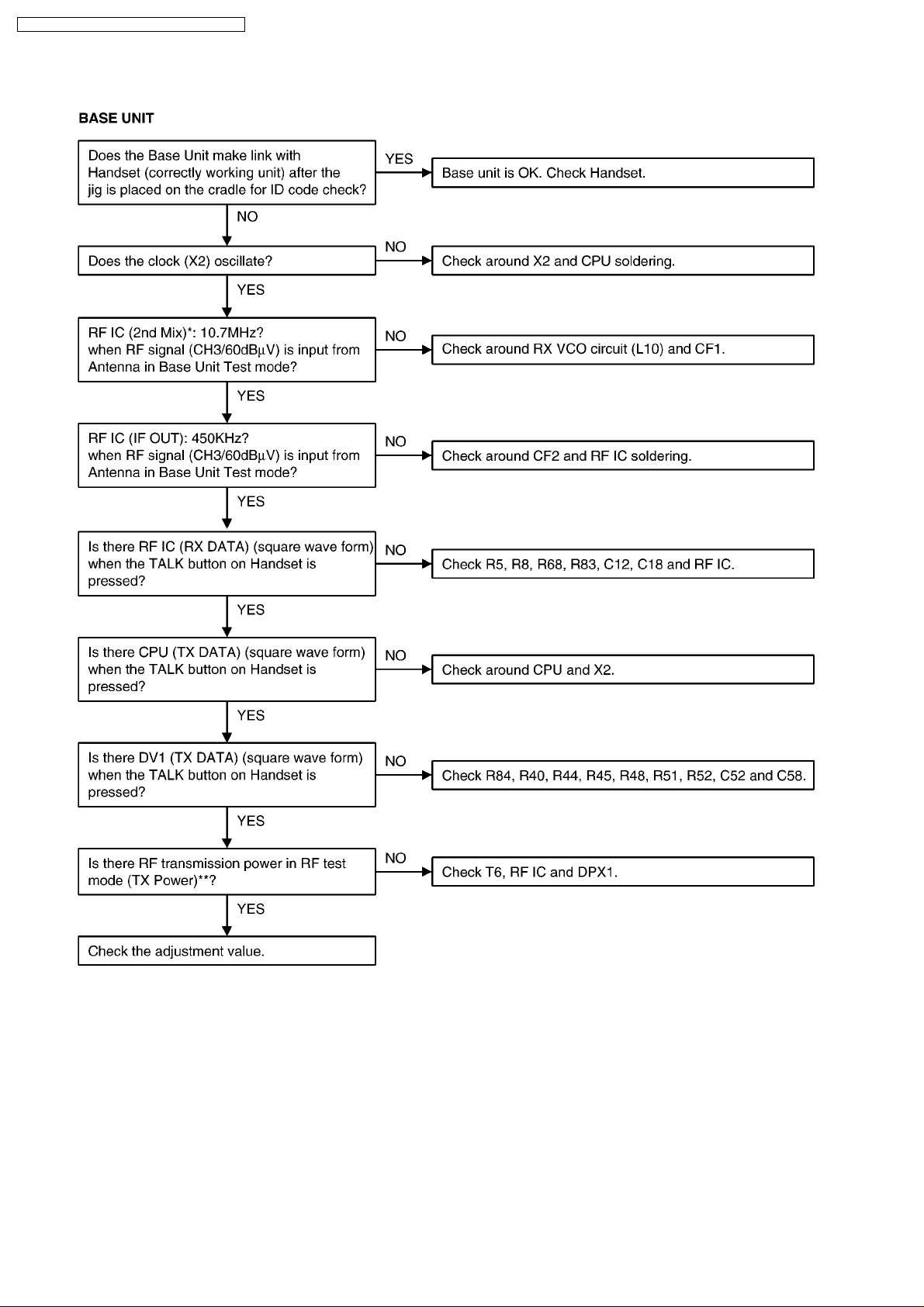
10.4. Check Link
**: Refer to Adjustment (P.26) Note:
CPU: IC2
RF IC: IC1
*: Each measurement points are shown in CIRCUIT BOARD (Base Unit) (P.67) or CIRCUIT BOARD (Handset) (P.69)
22
Page 23

KX-TC2000NZB / KX-TC2000NZW / KX-TC2000NZF
**: Refer to Adjustment (P.29). Note:
CPU: IC2
RF IC: IC1
*: Each measurement points are shown in CIRCUIT BOARD (Base Unit) (P.67) or CIRCUIT BOARD (Handset) (P.69)
23
Page 24

KX-TC2000NZB / KX-TC2000NZW / KX-TC2000NZF
10.5. Check Handset Transmission
Cross Reference:
Signal Route (P.46)
10.6. Check Handset Reception
Cross Reference:
Signal Route (P.46)
*: Each measurement points are shown in CIRCUIT
BOARD (Base Unit) (P.67) or CIRCUIT BOARD (Handset)
(P.69)
24
Page 25

KX-TC2000NZB / KX-TC2000NZW / KX-TC2000NZF
11 ADJUSTMENTS (BASE UNIT)
If your unit have below symptoms, adjust or confirm each item using remedy colum n from the table.
Symptom Remedy*
The base unit dose not respond to a call from handset. Make confirmation in item (A)
The base unit dose not transmit or the transmit f requency is off. Make adjustments in item (B)
The transmit frequency is off. Make adjustments in item (C)
The transmit power output is low, and the operating distance between the base unit and
the handset is less than normal.
The reception sensitivity of base unit is low with noise. Make confirmation in item (E)
The transmit level is high or low. Make confirmation in item (F)
The reception level is high or low. Make confirmation in item (G)
The unit does not link. Make confirmation in item (H)
*: Refer to Adjustment (P.26).
11.1. Test Mode Flow Chart (Base Unit)
The operation-flow of Test mode and main check items are shown below.
Make adjustments in item (D)
Note:
**: Refer to the above table.
25
Page 26

KX-TC2000NZB / KX-TC2000NZW / KX-TC2000NZF
11.2. How to change the channel
*: Refer to Flow Solder Side View (P.68).
11.3. Adjustment
Adjustment Items Test Mode Adjustment
(A) RX VCO
Confirmation
(B) TX VCO
Adjustment
(C) TX Frequency
Adjustment
(D) TX Power
Adjustment
(E) RX Sensitivity
Confirmation
(2nd IF output)
(F) Line Output Level
Confirmation
(G) Line Input
Modulation
Confirmation
(H) Noise Squelch
Confirmation
3ch Talk -
3ch Talk T6
3ch Talk VC1
3ch Talk T5
3ch Talk T2 1. Apply 60dBuVemf output from S.S.G. (modulation frequency 1KHz, dev.
3ch Talk - 1. Apply 60dBuVemf output from S.S.G. (modulation frequency 1KHz, dev.
3ch Talk - 1. Input via loop simulator 1.0KHz, -20dBm (measured at T-R) signal.
3ch Talk - 1. Measure the SSG output level when the noise squelch changes from Low
Point
•
• Confirm so that the reading of the Digital Voltmeter is 2.0V ± 1.0V.
• •
•
• Adjust T6 so that the reading of the Digital Voltmeter is 2.0V ± 0.3V.
• •
•
• Adjustment VC1 so that the reading of the frequency counter is
• •
30.1750MHz ± 100Hz.
•
• Adjust T5 so that the reading of the RF VTVM is more than 9dBm.
• •
0KHz).
2. Confirm that the reading of RF VTVM is the maximum value (more than
20mV)
3KHz).
2. Confirm that the reading of AF VTVM is more than 120mV (600Ω load).
2. Apply 60dBuVemf output from S.S.G. (modulation frequency 1KHz, dev.
0KHz).
3. Confirm so that the reading of FM Deviation Meter is 2.8KHz ±0.3KHz.
to High.
2. Confirm that the SSG output level is -10 ~ +5dBuVemf.
*Procedure Check or
* : The connection of adjustment equipment are as shown in Adjustment Standard (Base Unit) (P.27).
SSG Frequency: 39.875 MHz
Replace
Parts
IC1, L10,
C26, R14
IC1, DV1,
T6
IC, X1, T6,
DV1, C35,
C40, VC1
IC1, Q3,
Q4, Q5,
T5, DPX1
DPX1, T2,
CF1, CF2
IC1, Q11
IC1, DV1
IC1, DPX1
26
Page 27

11.4. Adjustment Standard (Base Unit)
When connecting the Simulator and Equipments for checking, please refer to the illustration below.
Q5
C83
C124
C57
Q2
(G)
(C)
(D)
R154
R40
ZD5
R52
R45
R38
R36
R54
Audio
Analyzer
27
DC12V or
AC adaptor
AF OSC
Loop
SIMULATOR
AF Volt Meter (F)
ZD10 ZD12
R160
R161
ZD11
R132
Q14
TXPOWER TXGND
C136
R175
C5
C96
C99
D11
Q17
R131
R120
R145
R138
R137
C14
Q25
FM Deviation
Meter
Frequency
Counter
RF
Volt Meter
50Ω
SSG
48.86MHz
C133
C62
C46
C47
R56
C56
R53
R42
C49
C51
R130
Q4
R111
C58
R48
R181
C123
ZD3
C59
R43
R35
R37
C53
R55
Q3
C60
R46
C55
R41
R33
D8
R198
C122
R116
R124
C52
R44
C48
C110
R51
C54
R155
R80
D1
R49
C40
R15
R16
C31
C45
R110
C61
Q6
R112
C29
R50
C125
R30
R86
Confirmation of VCO voltage
DC Volt Meter
(A), (B)
TX-VCORX-VCO
C6
R12
C23
R23
C39
C22
C44
1
C34
C109
C19
R25
R32
C36
R26
R22
R14
C26
R60
C27
C43
C35
C37
R31
R24
R148
R149
R183
IC1
R170
Q20
C101
C7
C33
R19
R20
R21
C93
R2
C79
C11
R143
R150
R13
R166
C16
C10
C24
C121
RF Volt
Meter
C9
R10
R6
R100
C86
R117
C120
R139
(E)
T.P ( CH change at test mode)
R108
C74
R406
R405
C65
R153
R134
R177
R178
R96
C107
R93
C88
R74
R140
C75
R105
Q402
LED1
R409
Q21
1
Q16
R407
C402
R76
R85
R179
R94
R81
R18
Q13
R79
C84
R408
R167
IC2
R78
C70
R410
R63
R158
R89
R77
Q403
R75
R115
R157
C135
R401
C92
R119
Q11
R122
R133
R59
R87
C90
R129
R159
R403
R404
C401
R402
R146
R84
C108
C85
Q401
R82
R123
KX-TC2000NZB / KX-TC2000NZW / KX-TC2000NZF
R126
R58
R1
C2
C8
R156
C67
R3
R5
C4
R7
C12
C18
R8
C73
R97
C63
R180
C28
R4
C25
R88
R103
C134
Q7
R114
R68
C64
C106
R185
R57
R109
C77
R197
R83
R62
R141
C82
IC3
R104
1
C69
R90
R95
C72
Note: (A) - (H) is refered to ADJUSTMENTS (BASE UNIT) (P.25)
Oscilloscope (H)
Page 28

KX-TC2000NZB / KX-TC2000NZW / KX-TC2000NZF
12 ADJUSTMENTS (HANDSET)
If your unit have below symptoms, adjust or confirm each item using remedy column from the table.
Symptom Remedy*
The movement of Battery Low Indicator is wrong. Make confirmation in item (A)
The base unit does not respond to a call from the handset. Make adjustments in item (B)
The base unit does not transmit or the transmit frequency is off. Make confirmation in item (C)
The transmit frequency is off. Make adjustments in item (D)
The transmit power output is low, and the operating distance between the base unit and
the Handset is less than normal.
The reception sensitivity of the handset is low with noise. Make confirmation item (F)
Does not link between the base unit and the handset. Make confirmation in item (G)
The reception level is high or low. Make confirmation item (H)
The transmit level is high or low. Make confirmation in item (I)
*: Refer to Adjustment (P.29).
Unit condition:
1. Remove the antenna lead wire from P.C Board of the handset.
2. Power Supply: DC 3.9V (DC power supply)
3. Volume: HIGH (When P.C. Board of handset is in test mode, volume condition is medium. Press “LOCATOR” key once.)
4. Speaker Load: 150Ω
CH TX Frequency RX Frequency
CH3 39.875MHz 30.175MHz
Make confirmation in item (E)
12.1. Test Mode Flow Chart (Handset)
Note:
Refet to CIRCUIT BOARD (Handset) (P.69)
Signal Route (P.46)
28
Page 29

12.2. How to change the channel
12.3. Adjustment
KX-TC2000NZB / KX-TC2000NZW / KX-TC2000NZF
Adjustment Items Test Mode Adjustment
(A) Battery Low
Confirmation
(B) TX VCO
Adjustment
(C) RX VCO
Confirmation
(D) TX Frequency
Adjustment
(E) TX Power
Confirmation
(F) RX Sensitivity
Confirmation
(2nd IF output)
(G) Noise Squelch
Confirmation
(H) Speaker
Output Level
Confirmation
(I) Mic Modulation
Factor
Confirmation
(J) Data
Modulation
Confirmation
(K) Battery low
Confirmation
3ch Talk - 1. Adjust the power supply voltage to DC3.60V,and confirm so that the
3ch Talk T6 1. Adjust T6 so that the reading of the Digital Voltmeter is 1.5V ± 0.3V. IC1, X1,
3ch Talk - 1. Confirm so that the reading of the Digital Voltmeter is 0.7 ~ 3.0V. IC1, X1,
3ch Talk VC1
3ch Talk -
3ch Talk T3 1. Apply 60dBuVemf output from S.S.G. (modulation frequency 1KHz, dev.
3ch Talk - 1. Measure the SSG output level when the noise squelch changes from
3ch Talk - 1. Apply 60dBuVemf output from S.S.G. (modulation frequency 1KHz, dev.
3ch Talk - 1. Apply a MIC signal (1KHz, 5.0mV at 600Ω load).
3ch Talk -
- - 1. Apply 3.50V between BATT(+) and BATT(-).
Point
Procedure Check or
reading of oscillosope is High.
2. Adjust that power supply voltage to DC 3.40V, and confirm so that the
reading of oscilloscope is Low.
•
• Adjust VC1 so that the reading of the frequency counter is 39.8750MHz
• •
± 100Hz.
•
• Confirm so that the reading of the RF VTVM is more than -3.0dBm
• •
(50Ω load).
0KHz).
2. Confirm that the reading of RF VTVM is the maximum value (more than
15mV).
Low to High. (modulation frequency 1KHz, dev.3kHz)
2. Confirm that the SSG output level is -18 ~ 0dBuVemf.
3KHz).
2. Confirm that the reading of AF VTVM is more than 30mV.
(distortion: less than 5%) (volume High).
2. Confirmation so that the reading of FM Deviation Meter is 3.4KHz ±
0.4KHz.
•
• Confirm for 5.0 ± 1.0KHz FM Deviation Meter reading.
• •
2. Confirm that there is no flashing of RECHARGE LED.
3. Apply 3.40V between BATT(+) and BATT(-).
4. Confirm that there is flashing of RECHARGE LED.
Replace
Parts
IC1
T6, DV1
L6, C24
IC1,
DPX1, T5
IC1,Q3,Q4,
Q5, DPX1
DPX1,
T3,IC1,
CF1, CF2
IC1, DPX1
IC1
IC1, DV1
IC1
The connections of adjustment equipment are as shown in Adjustment Standard (Handset) (P.30).
SSG Frequency: 30.175 MHz
29
Page 30

12.4. Adjustment Standard (Handset)
When connecting the Simulator and Equipments for checking, please refer to the illustration below.
(Component View)
KX-TC2000NZB / KX-TC2000NZW / KX-TC2000NZF
30
C37
REC
C56
C51
L1
DV1
VC1
C43
150Ω
C42
AF Volt Meter (H)
X1
R101
R11
C31
T6
C15
L6
T5
L200
R106
C29
R28
C38
C23
R14
C26
CF1
C27
T3
R21
R93
C34
C77
C76
R108
R94
R95
R110
C8
DPX1
C18
C75
C12
R109
C1
CF2
Q1
T1
C32
R16
C16
C9
R5
C30
R18
R8
R6
R46
R98
R37
C64
R87
R74
C73
R78
R99
C69
C72
R86
R85
R39
Q4
D1
R30
R29
C79
R102
R23
R103
C33
BZ1
R3
C14
R55
D3
R63
C78
R42
R17
R61
R20
Q3
Q2
Q7
R19
R22
C39
R54
R105
R56
Q8
Q12
C58
R48
R107
C46
R70
X3
C45
X2
R58
R69
R77
R67
R66
R57
R12
R79
R62
R71
R72
R112
R59
R80
R73
IC2
C66
R81
C65
R83
C84
C68
C71
C70
C67
R84
R96
R82
R64
C74
R76
R53
R75
R65
R111
R68
R60
Q11
L3
C63
R36
ZD1
C80
CHG+ CHG-
L5
47µF
C86
ZD3
L4
+
-
BATT1
C48
Q9
L2
L7
(A) Battery Low
AFGenerator
(G) Noise Squelch
Oscilloscope
Note: (A)-(I) is refered to ADJUSTMENTS (HANDSET) (P.28)
Page 31

(Flow Solder Side View)
31
TX VCO
DC Volt Meter(B)
Audio
Analyzer
(E)
(D)
(I), (J)
SSG
43.820MHz
RF Millivolt
Meter
Frequency
Counter
FM Deviation
Meter
R52
C62
Q6
C57
R44
R40
R38
C52
C61
R50
R24
C40
C59
R45
C4
R49
C60
R41
C36
C49
C10
R47
C41
50Ω
(F)
RF
Volt Meter
TXPOWERTXGND
C55
R43
R97
C50
Q5
C53
R51
C44
C47
R200
C201
C54
R35
R34
C35
R26
C24
C88
C3
C202
Q200
C200
C17
R1
R25
C203
R201
C6
C5
IC1
C28
C89
C7
C22
C2
C21
R13
C85
C13
R9
R113
R10
DIRTAUTO
TALK
LED5
R2
3
21
LED2
6
LED1
K11
45
9
LED4
LED3
78
#
0
REDIALRINGER
FLASH
PAUSE
LOUDPROG
CH
MIC1
LED6
RX VCO
DC Volt Meter(C)
Note: (A)-(I) is refered to ADJUSTMENTS (HANDSET) (P.28)
DC Power
Supply
KX-TC2000NZB / KX-TC2000NZW / KX-TC2000NZF
Page 32

KX-TC2000NZB / KX-TC2000NZW / KX-TC2000NZF
13 RF SPEC IFICATION
13.1. Base Unit
Item Value Refer to -.* Remarks
TX Frequency 30.175MHz ± 100Hz ADJUSTMENTS (BASE UNIT) (C) at CH3
TX Power more than 1mW ADJUSTMENTS (BASE UNIT) (D) at CH3
Line Modulation factor 2.5 kHz~3.1 kHz ADJUSTMENTS (BASE UNIT) (G)
Data Modulation factor 4.5 kHz~7.5 kHz —
Line Output level more than 120mV —
*: Refer to Adjustment (P.26).
13.2. Handset
Item Value Refer to -.** Remarks
TX Frequency 39.875 MHz ± 0.1kHz ADJUSTMENTS (HANDSET) (D) at CH3
TX Power more than 1mW ADJUSTMENTS (HANDSET) (E) at CH3 (Antenna
Data Modulation factor 5.0 kHz~6.0 kHz ADJUSTMENTS (HANDSET) (J) at CH3
MIC Modulation factor 2.9 kHz/dev~3.8 kHz/dev ADJUSTMENTS (HANDSET) (I) at CH3 (MIC terminal
SP Output level more than 30mV —
soldering point 50Ω
Load)
2.4mV Input)
**: Refer to Adjustment (P.29).
14 HOW TO CHECK THE HANDSET SPEAKER
1. Prepare the digital voltmeter, and set the selector knob to ohm meter.
2. Put the probes at the speaker terminals as shown below.
32
Page 33

KX-TC2000NZB / KX-TC2000NZW / KX-TC2000NZF
15 FREQUENCY TABLE (MHz)
BASE UNIT PORTABLE UNIT
Channel Transmit Frequency Receive Frequency Transmit Frequency Receive Frequency
1 30.0750 39.7750 39.7750 30.0750
2 30.1250 39.8250 39.8250 30.1250
3 30.1750 39.8750 39.8750 30.1750
4 30.2250 39.9250 39.9250 30.2250
5 30.2750 39.9750 39.9750 30.2750
6 30.1000 39.8000 39.8000 30.1000
7 30.1500 39.8500 39.8500 30.1500
8 30.2000 39.9000 39.9000 30.2000
9 30.2500 39.9500 39.9500 30.2500
10 30.3000 40.0000 40.0000 30.3000
33
Page 34

KX-TC2000NZB / KX-TC2000NZW / KX-TC2000NZF
16 EXPLANATION OF CPU DATA C OMMUNICATION
16.1. STAND-BY -> TALK, TALK -> STAND-BY
*: The channel is changed if the noise interferes with the conversation.
34
Page 35

16.2. Ringing
KX-TC2000NZB / KX-TC2000NZW / KX-TC2000NZF
35
Page 36

KX-TC2000NZB / KX-TC2000NZW / KX-TC2000NZF
16.3. Changing the Channel
36
Page 37

16.4. Ports for transmitting and receiving of data
KX-TC2000NZB / KX-TC2000NZW / KX-TC2000NZF
Handset:
transmitting (TX) ... 36 Pin
receiving (RX) ... 4 Pin
Base Unit:
transmitting (TX) ... 17 Pin
receiving (RX) ... 10 Pin
16.5. Waveform of DATA used for cordless transmission and reception
The DATA which is transmitted from the Handset to the Base Unit is combination of DATA 0, DATA 1, PSEUD.
The DATA which is transmitted from the Base Unit to the Handset is combination of DATA 0, DATA 1, PSEUD.
16.5.1. Handset
16.5.2. Base Unit
•
• For example (one of part of data)
• •
37
Page 38

17 BLOCK DIAGRAM (BASE UNIT)
KX-TC2000NZB / KX-TC2000NZW / KX-TC2000NZF
38
H/S
DUPLEXER
DPX1
RX LOOP
TX LOOP
RF AMP
Q3,Q4, T5
ANTENNA
X1
RX VCO
L10, C26
RF AMP
Q1, T2
POWER
CONTROL
Q2
TX VCO
Q5, T6, DV1
VC1
10.7MHz 450kHz
RF FILTER
CF1, CF2
RF IC
MIX 1/2
PLL OSC
DC 5V
IC1
RF
-DATA
-CLK
-STB
EXP
COM
X2
17
14
TELEPHONE LINE
INTERFACE
TEL
LINE
AMP
Q11, IC3
POWER SUPPLY
RESET CHARGE
5V
REGULATOR
Q18, Q19
TEL
LINE
SW
T7
DIODE
BRIDGE
D2, D3,
D4, D5
DC IN
12V 150mA
(AC Adaptor)
AC DOWN
DTC
Q402,Q403
TEL LINE
DC 5V
CONTROL LINE
AUDIO SIGNAL
LED
Q21, LED1
VTX RF
TX
DATA
-DATA
-CLK
-STB
RX
DATA
CPU
IC2
RESET
DTC
Q401
CHARGE
DTC
Q7
CHARGE
CONTROL
Q14, Q17
Q24, Q25
DC 12V
CHARGE
TERMINAL
KX-TC2000NZB/W/F BLOCK DIAGRAM (BASE UNIT)
Page 39

18 BLOCK DIAGRAM (HANDSET)
39
Base
DUPLEXER
DPX1
RX LOOP
TX LOOP
RF AMP
Q5, T5
Q200
ANTENNA
X1
RX VCO
L6, C24
RF AMP
Q1, T3
POWER
CONTROL
Q4
TX VCO
Q6, T6, DV1
VC1
MIX 1/2
PLL OSC
DC 3.9V
RF FILTER
CF1, CF2
RF IC
IC1
RF
-DATA
-CLK
-STB
EXP
COM
X3
SPEAKER
REC1
MIC
MC1
DIODE
BRIDGE
Q9
DC 3.9V
CONTROL LINE
AUDIO SIGNAL
BATTERY
3.9V
LED
Q8, LED 1-4
KEY BOARD
VTX
TX
DATA
RF
-DATA
-CLK
-STB
DATA
CPU
IC2
RX
RESET
Q11
CHARGE
DTC
IC2 PING37
BUZZER
Q7, BZ1
Q12
DIODE
BRIDGE
D1
CHARGE
TERMINAL
KX-TC2000NZB/W/F BLOCK DIAGRAM (HANDSET)
KX-TC2000NZB / KX-TC2000NZW / KX-TC2000NZF
Page 40

KX-TC2000NZB / KX-TC2000NZW / KX-TC2000NZF
19 CIRCUIT OPERATION
19.1. Outline
Base unit consists of the following ICs as shown in BLOCK DIAGRAM.
•
• CPU:IC2
• •
−
− Controlling the whole system
− −
−
− Forming/analyzing all data signals (ACK, CMD signal etc.*)
− −
−
− All interfaces (ex: LED, KEY, SP, Mic, LCD, Detector Circuit (Charge/ Power Down)
− −
*Refer to EXPLANATION OF CPU DATA COMMUNICATION (P.34).
•
• RF IC:IC1
• •
−
− PLL Oscillator
− −
−
− Detection
− −
−
− Compress/ Expander
− −
−
− first/ second mixer
− −
−
− Amplifier for transmission and reception
− −
•
• Additionally,
• •
−
− Power Supply Circuit
− −
−
− Reset Circuit
− −
−
− Charge Circuit
− −
−
− Telephone Line Interface Circuit
− −
Handset consist of the following ICs as shown in BLOCK DIAGRAM.
•
• CPU: IC2
• •
−
− All data signals (forming/analyzing ACK or CMD signal*)
− −
−
− All interfaces (ex; LED, Key, Buzzer, Detector Circuit, Charge, Battery Low)
− −
−
− RAM for keeping the data (CH Number, ID Code, etc.)
− −
•
• RF IC:IC1
• •
−
− PLL Oscillator
− −
−
− Detector
− −
−
− Compress/Expander
− −
−
− first, second mixer
− −
−
− Amplifier for transmission and reception
− −
*Refer to EXPLANATION OF CPU DATA COMMUNICATION (P.34).
40
Page 41

KX-TC2000NZB / KX-TC2000NZW / KX-TC2000NZF
19.2. Power Supply Circuit
The power supply to the CPU (Digital, Analog) and RF IC from AC Adaptor (+12V) is shown in the diagram below.
The base unit power supply is DC12V. The handset´s power is supplied from 3.6V battery (Nickel-Cadmium battery) which is
installed in the handset.
Power supply for transmitter is turned on by a press of "Talk" key on the handset. During the stand-by mode, the unit stops
transmitting but receives the signal.
Also during on-hook condition (the handset is placed on the base unit), backup power for memory of the last dialed number is
supplied through the battery. The memory of this unit is not backed up by the current from
the telephone line.
The base unit DC power supply is regulated by Q18, the CPU power is regulated by Q19. The Q401, Q403 detects AC Adaptor
power failure and maintains the unit security code.
Fig. 1
41
Page 42

KX-TC2000NZB / KX-TC2000NZW / KX-TC2000NZF
19.3. Reset Circuit (Base Unit)
After power supply from AC adaptor, the below circuit is for making reset signal. Refer to the below waveform.
Fig. 2
Fig. 3
42
Page 43

KX-TC2000NZB / KX-TC2000NZW / KX-TC2000NZF
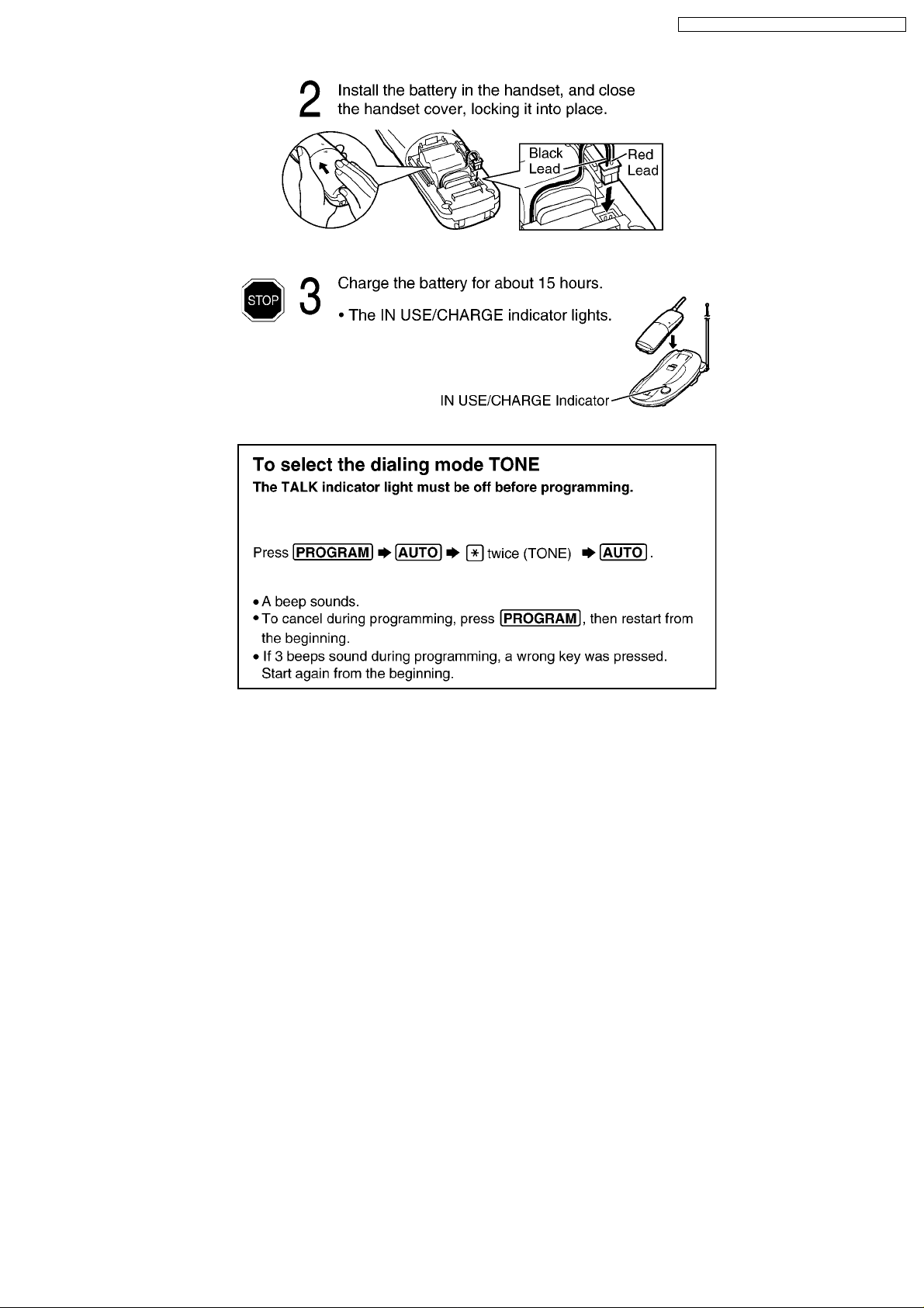
19.4. Charge Circuit
Circuit Operation:
When charging the handset on the base unit, the charge current is as follows;
DC (JK2) → L8 → D6 → Q14 → Q24 → L7 → CHG+(Base) → [CHG+(Handset) → L4 → Q9 → BATT(1)....Battery....BATT(2)
→ L5 →
CHG-(Handset)] → CHG-(Base) → L5,
In this way, the CPU on both unit detects the fact that the battery is charged.
The charge current is controlled by switching Q24, Q25 of Base Unit. The battery is charged in normal mode for 15 hours and
then in trickle mode.
19.5. Telephone Line Interface
Function:
•
• Bell signal detection
• •
•
• ON/OFF hook and pulse dial circuit
• •
•
• Side tone circuit
• •
Bell signal detection and OFF HOOK circuit:
In the idle mode, Q103 is open to cut the DC loop current and decrease the ring load. When ring voltage appears at the Tip (T)
and Ring (R) leads (When the telephone rings), the AC ring voltage is transferred as follows:
JK1 (3): T → L6 → R184 → R144 → IC3D (12,13 → 14) → C97 → R148 → Q20 → IC2 (24) [BELL]
JK1 (2): R → L4 → R183 → R152 →↑
When the CPU (DSP) detects a ring signal and press the TALK Key on the handset. Q6 turns on and then RY1 turns on,
thus providing an off-hook condition (active DC current flow through the circuit) and the following signal flow is for the loop
current.
T → R160 → L4 → D2 → RY1 → R107 → T7 → R116 → D5 → L6 → R161 → R[OFF HOOK]
ON HOOK Circuit:
Q6 is open, RY1 disconnected as to cut the DC loop current and to cut the voice signal. The unit is consequently in an on-hook
condition.
Side Tone Circuit:
Basically this circuit prevents the TX signal from feeding back to RX signal.
As for this unit, TX signal feed back from Q11 is canceled by the cancellor circuit of AGC.
19.6. DTMF
The DTMF signal is generated by five outputs of IC2 (CPU) and output to telephone line through the filter of IC3A which is a
lowpass filter as shown below.
The combination of five outputs “1”, “0” makes 32 (=2
generator.
5) level signals and makes smooth waveform after filter like a DTMF
43
Page 44

KX-TC2000NZB / KX-TC2000NZW / KX-TC2000NZF
19.7. Transmitter/Receiver
Base Unit and Handset are mainly consists of RF(Radio Frequency) IC and CPU.
Base Unit and Handset transmit/receive voice signal and data signal through the antenna on carrier frequency.
Signal Pass :
*Refer to CDL TX/RX in Signal Route (P.46).
19.7.1. Base to Handset
Circuit Operation:
The voice signal input from the TEL LINE interface goes to RF IC as shown in
BLOCK DIAGRAM (BASE UNIT) (P.38).
In the talk mode (off-hook) condition, the telephone line voice signal passes through D2, D3, D4, D5, RY1 (Relay), R107 and
T7.
The other party´s voice signal is coupled with T7 and amplified by Q11 and led to IC3-B (OP Amplifier device).
And the signal goes through the compressor of RF IC, it is output to transmitter circuit.
The signal of the data sent to the handset is applied in the anode of the variable capacitor diode (VARICAP : DV1).
The capacitor of VARICAP is changing in accordance with the voice signal from telephone line interface or TX DATA signal from
CPU. Therefore, the carrier frequency which is generated by TXVCO will be changing, and Frequency modulated RF
signal is generated and amplified by RF AMP(Q3, Q4, T5). It pass through the Duplexer DPX1 and radiated from Antenna.
The signal is transmitted from the base unit and received by the handset antenna and amplified by RF amplifier (Q1) through
DPX1 as shown in BLOCK DIAGRAM (HANDSET) (P.39). And then it is converted to 10.7 MHz and 455 KHz Intermediate
frequency by RF IC and related components.
The demodulated audio signal is output from RF IC (DET OUT) and passed through "Expander" process to reduce noise, then
voice signal amplified by "Receiver amplifier" is output to receiver (REC1).
The receiver loudness is adjustable using "LOUD" key on the handset. Q2 and Q3 control the volume. When CPU (VOL1)
becomes low, the volume becomes "MID", while CPU (VOL1, 2) become low, the volume becomes "HIGH".
TX data (to Handset)
CPU (VTX) becomes low to turn on the transmission power transistor Q2, and CPU (TX-data) sends data signal. It is
FM-modulated by TXVCO and driven by RF AMP, then transmitted to the handset.
44
Page 45

KX-TC2000NZB / KX-TC2000NZW / KX-TC2000NZF
19.7.2. Handset to Base
Circuit Operation:
The voice signal from the handset user is picked up by the microphone (MC1), voice signal passes through "Compressor"
process to reduce noise as shown in BLOCK DIAGRAM (HANDSET) (P.39). And the voice is FM-modulated by
VARICAP (DV1).
The carrier frequency is generated by TX VCO. The transmitter power transistor Q4 is turned on/off by CPU (VTX).
The carrier signal is amplified by RF AMP and sent to the handset duplexer and antenna.
The signal of 39MHz band (39.775~40.000MHz) which is input from ANT is filtered at DPX1 as shown in
BLOCK DIAGRAM (BASE UNIT) (P.38), then it is input to RF IC.
The signal input to RF IC is converted through Mixer inside of RF IC, RF filter (CF1, CF2) and Expander.
The signal is transmitted from the handset and received by the base unit antenna and amplified by RF amplifier Q1, then
it is converted to10.7 MHz and 450 KHz Intermediate by RF IC. The demodulated audio signal is output from RF IC
(DET OUT) and passed through "Expander" process to reduce noise, then voice signal is led to LINE AMP. The signal is
passed through TELEPHONE INTERFACE and Tel-line.
RX data (from Handset):
The data signal from handset (ex: Talk, ACK, COM) is also included in 39 MHz band same as the voice data. After second if
filter, the data signal is made square shape by data limiting AMP of the RF IC. RX data is output to CPU (RX Data).
19.7.3. RF signal operation/control and PLL operation (RF UNIT)
Base unit radio frequency signal received by antenna passes through duplexer (DPX1).
RF signal is amplified by RF AMP. RF signal received from RF IC is mixed with RX local frequency at Mixer to generate
10.7 MHz wide band IF. The reference frequency is generated by X1 11.150 MHz crystal. VC1 is the reference frequency
for adjustment. The 10.7 MHz is mixed with reference and 450KHz narrow band IF is generated. The demodulation audio signal
is adjusted to the maximum at T1. RF IC is controlled by CPU (RF_STB, DATA, CLK). The RX local frequency is generated
by RXVCO.
45
Page 46

KX-TC2000NZB / KX-TC2000NZW / KX-TC2000NZF
19.8. Signal Route
Each signal route is as follows.
46
Page 47

KX-TC2000NZB / KX-TC2000NZW / KX-TC2000NZF
20 CIRCUIT OPERATION (HANDSET)
20.1. Reset Circuit (Handset)
The power of handset is supplied by battery.
Whenever the battery is recharged or inserted, the impulse at CHG+ becomes Reset signal through Q11, and sent to CPU.
Fig. 4
Fig. 5
47
Page 48

KX-TC2000NZB / KX-TC2000NZW / KX-TC2000NZF
20.2. Battery Low / Power Down Detector
Circuit Operation:
“Battery Low” and “Power Down” are detected by RF IC which check the voltage from battery. Shortly, every detected blocks
are inside of RF IC. The detected voltage is as follows;
•
• Battery Low
• •
Battery voltage : V(Batt) < 3.457V
The CPU detects this level and “Recharge battery” LED starts flashing.
•
• Power Down
• •
Battery voltage : V(Batt) < 3.0V
The output of RF IC (P-DOWN) becomes low level, then CPU stops working to keep the data (CH number, ID Code, etc.)
Fig. 6
48
Page 49

21 CPU DATA (Base Unit)
21.1. IC2
KX-TC2000NZB / KX-TC2000NZW / KX-TC2000NZF
49
Page 50

KX-TC2000NZB / KX-TC2000NZW / KX-TC2000NZF
22 CPU DATA (Handset)
22.1. IC2
50
Page 51

23 RF IC (Base Unit and Handset)
23.1. IC1
KX-TC2000NZB / KX-TC2000NZW / KX-TC2000NZF
51
Page 52

KX-TC2000NZB / KX-TC2000NZW / KX-TC2000NZF
24 HOW TO REPLACE FLAT
PACKAGE IC
24.1. Preparation
•
• SOLDER
• •
Sparkle Solder 115A-1, 115B-1 or Almit Solder KR-19, KR19RMA
•
• Soldering iron
• •
Recommended power consumption will be between 30 W
to 40 W.
Temperature of Copper Rod 662 ± 50°F (350 ± 10°C)
(An expert may handle between 60 W to 80 W iron, but
beginner might damage foil by overheating.)
•
• Flux
• •
HI115 Specific gravity 0.863.
(Original flux will be replaced daily.)
24.2. Procedure
1. Temporary fix FLAT PACKAGE IC by soldering on two
marked2pins.
24.3. Modification Procedure of
Bridge
1. Re-solder slightly on bridged portion.
2. Remove remained solder along pins employing soldering
iron as shown in below figure.
*Most important matter is accurate setting
of IC to the corresponding soldering foil.
2. Apply flux for all pins of FLAT PACKAGE IC.
3. Solder employing specified solder to direction of arrow, as
sliding the soldering iron.
52
Page 53

KX-TC200 0NZB / KX-TC2000NZW / KX-TC200 0NZ F
25 CABINET AND ELECTRICAL PARTS LOCATION (BASE
UNIT)
53
Page 54

KX-TC200 0NZB / KX-TC2000NZW / KX-TC200 0NZ F
26 CABINET AND ELECTRICAL PARTS LOCATION
(HANDET)
54
Page 55

27 ACCESSORIES AND PACKING MATERIALS
KX-TC200 0NZB / KX -TC2000N ZW / KX-TC2000NZF
55
Page 56

KX-TC2000NZB / KX-TC2000NZW / KX-TC2000NZF
28 REPLACEMENT PARTS
LIST
Note:
1. RTL (Retention Time Limited)
The marking (RTL) indicates that the Retention Time is
limited for this item.
After the discontinuation of this assembly in production, the
item will continue to be available for a specific period of
time. The retention period of availability depends on the
type of assembly and the laws governing parts and product
retention.
At the end of this period, the assembly will no longer be
available.
2. Important safety notice
Components identified by the
characteristics important for safety. When replacing any of
these components, only use specified manufacture´s parts.
3. The S mark indicates service standard parts and may differ
from production parts.
4. RESISTORS & CAPACITORS
Unless otherwise specified;
All resistors are in ohms (Ω) K=1000Ω, M=1000kΩ
All capacitors are in MICRO FARADS (µF) P=µµF
*Type & Wattage of Resistor
28.1. Base Unit
28.1.1. CABINET AND ELECTRICAL
PARTS
Ref.
No.
1 PQJT10180Z CHARGE TERMINAL
2 PQHR10998Z LED LENS
3 PQGT16253Z NAME PLATE (for KX-TC2000NZB)
3 PQGT16257Z NAME PLATE (for KX-TC2000NZF)
3 PQGT16255Z NAME PLATE (for KX-TC2000NZW)
4 PQQT22294Z CHARGE LABEL
5 PQBC10389Z1 LOCATOR BUTTON (for KX-
Part No. Part Name & Description Remarks
TC2000NZB)
mark indicates special
Ref.
No.
5 PQBC10389Y2 LOCATOR BUTTON (for KX-
5 PQBC10389Z3 LOCATOR BUTTON (for KX-
6 PQKE10335Z1 HOOK LEVER (for KX-TC2000NZB)
6 PQKE10335Z2 HOOK LEVER (for KX-TC2000NZF)
6 PQKE10335Z5 HOOK LEVER (for KX-TC2000NZW)
7 PQKF10597Z1 LOWER CABINET (for KX-
7 PQKF10597Z3 LOWER CABINET (for KX-
8 PQKM10607X1 UPPER CABINET (for KX-
8 PQKM10607W3 UPPER CABINET (for KX-
8 PQKM10607X4 UPPER CABINET (for KX-
9 PQSA10105Y ANTENNA
10 PQKL10056Z1 WALL MOUNT ADAPTOR (for KX-
10 PQKL10056Z3 WALL MOUNT ADAPTOR (for KX-
11 LCBT9300013 FOOT RUBBER
Part No. Part Name & Description Remarks
TC2000NZF)
TC2000NZW)
TC2000NZB/F)
TC2000NZW)
TC2000NZB)
TC2000NZF)
TC2000NZW)
TC2000NZB/F)
TC2000NZW)
28.1.2. MAIN P.C.BOARD PARTS
Ref.
No.
PCB1 PQWPC2000ALH MAIN P.C.BOARD ASS´Y (RTL)
IC1 SA133122409 IC
IC2 SA138740A11 IC
IC3 SA1S0032402 IC
IC5 AB1L0081715 IC
Q1 BB230024104 TRANSISTOR(SI)
Q2 SB0I0390601 TRANSISTOR(SI)
Q3 SB1D0390401 TRANSISTOR(SI)
Q4 SB1D0390401 TRANSISTOR(SI)
Q5 SB1D0390401 TRANSISTOR(SI)
Q6 SB1I0390408 TRANSISTOR(SI)
Q7 SB1I0390408 TRANSISTOR(SI)
Q10 BB010009408 TRANSISTOR(SI)
Q11 SB1I0390408 TRANSISTOR(SI)
Q14 SB0I0390601 TRANSISTOR(SI)
Q17 SB1I0390408 TRANSISTOR(SI)
Q18 BB1M0390401 TRANSISTOR(SI)
Q19 BB1M0390401 TRANSISTOR(SI)
Q20 SB1I0390408 TRANSISTOR(SI)
Q21 SB1I0390408 TRANSISTOR(SI)
Q24 BB1M0390401 TRANSISTOR(SI)
Q25 SB1I0390408 TRANSISTOR(SI)
Q401 SB1I0390408 TRANSISTOR(SI)
Q402 SB0I0390601 TRANSISTOR(SI)
Q403 SB1I0390408 TRANSISTOR(SI)
D1 SC1GM414809 DIODE(SI)
D2 BC2W0400401 DIODE(SI)
D3 BC2W0400401 DIODE(SI)
D4 BC2W0400401 DIODE(SI)
D5 BC2W0400401 DIODE(SI)
D7 VA02700A401 DIODE(SI)
D8 SC1GM414809 DIODE(SI)
D11 SC1GM414809 DIODE(SI)
DV1 BC6K0025101 DIODE(SI)
ZD1 BC050474801 DIODE(SI)
ZD2 BC050474801 DIODE(SI)
ZD3 SC4555C4V71 DIODE(SI)
ZD4 BC4579C8V21 DIODE(SI)
ZD5 SC4555C4V71 DIODE(SI)
ZD8 BC4579C5V65 DIODE(SI)
ZD9 BC4579C5V65 DIODE(SI)
ZD10 SC4555C1506 DIODE(SI)
ZD11 SV110201203 DIODE(SI)
ZD12 SC4555C1506 DIODE(SI)
Part No. Part Name & Description Remarks
(ICS)
(TRANSISTORS)
(DIODES)
56
Page 57

KX-TC2000NZB / KX-TC2000NZW / KX-TC2000NZF
Ref.
No.
ZD404 BC4579C7V50 DIODE(SI)
LED1 SC5E0192115 LED
L1 PQLQZK3R3J COIL
L3 PQLQZM120J COIL
L4 PQLQZK120J COIL
L5 PQLQZK120J COIL
L6 PQLQZK120J COIL
L7 PQLQZK120J COIL
L10 PQLQZK1R2J COIL
L11 PQLQZM120J COIL
DPX1 BDFL0083004 COIL
JK1 DC72P120018 JACK
JK2 DC71P120023 JACK
CF1 BDFA107MA07 CERAMIC FILTER
CF2 BDFJ0450E08 CERAMIC FILTER
X1 BD1H1115002 CRYSTAL OSCILLATOR
X2 BD5H0795210 CRYSTAL OSCILLATOR
T1 CLIP1200053 TRANSFORMER
T2 CLIP1200100 TRANSFORMER
T5 CLIP1200096 TRANSFORMER
T6 CLIP1200142 TRANSFORMER
T7 DG0P1200035 TRANSFORMER
ZNR1 VA107D271K1 VARISTOR
R1 ERJ3GEYJ470 47
R2 ERJ3GEYJ331 330
R3 ERJ3GEYJ153 15K
R4 ERJ3GEYJ822 8.2K
R5 ERJ3GEYJ103 10K
R6 ERJ3GEYJ103 10K
R7 ERJ3GEYJ334 330K
R8 ERJ3GEYJ103 10K
R10 ERJ3GEYJ393 39K
R12 ERJ3GEYJ101 100
R13 ERJ3GEYJ623 62K
R14 ERJ3GEYJ103 10K
R15 ERJ3GEYJ562 5.6K
R16 ERJ3GEYJ153 15K
R18 ERJ3GEYJ222 2.2K
R19 ERJ3GEYJ563 56K
R20 ERJ3GEYJ184 180K
R21 ERJ3GEYJ273 27K
R22 ERJ3GEYJ472 4.7K
R23 ERJ3GEYJ104 100K
R24 ERJ3GEYJ103 10K
R25 ERJ3GEYJ683 68K
R26 ERJ3GEYJ154 150K
R30 ERJ3GEYJ104 100K
R31 ERJ3GEYJ473 47K
R32 ERJ3GEYJ105 1M
R33 ERJ3GEY0R00 0
R35 ERJ3GEYJ101 100
R36 ERJ3GEYJ224 220K
R37 ERJ3GEYJ101 100
R38 ERJ3GEYJ104 100K
R40 ERJ3GEYJ223 22K
R41 ERJ3GEYJ473 47K
R42 ERJ3GEYJ103 10K
R43 ERJ3GEYJ103 10K
R44 ERJ3GEYJ104 100K
R45 ERJ3GEYJ474 470K
R46 ERJ3GEYJ222 2.2K
R48 ERJ3GEYJ223 22K
R49 ERJ3GEYJ753 75K
R50 ERJ3GEYJ822 8.2K
R51 ERJ3GEYJ362 3.6K
Part No. Part Name & Description Remarks
(LED)
(COILS)
(JACKS)
(CERAMIC FILTERS)
(CRYSTAL OSCILLATORS)
(TRANSFORMERS)
(VARISTOR)
(RESISTORS)
Ref.
No.
R53 ERJ3GEYJ153 15K
R54 ERJ3GEYJ153 15K
R55 ERJ3GEYJ681 680
R56 ERJ3GEYJ222 2.2K
R57 ERJ3GEYJ224 220K
R58 ERJ3GEYJ221 220
R59 ERJ3GEYJ104 100K
R60 ERJ3GEYJ223 22K
R62 ERJ3GEYJ104 100K
R64 ERDS2TJ103 10K
R68 ERJ3GEYJ104 100K
R74 ERJ3GEY0R00 0
R75 ERJ3GEYJ103 10K
R77 ERJ3GEYJ203 20K
R78 ERJ3GEYJ393 39K
R79 ERJ3GEYJ823 82K
R80 ERJ3GEYJ222 2.2K
R81 ERJ3GEYJ164 160K
R82 ERJ3GEYJ103 10K
R83 ERJ3GEYJ103 10K
R84 ERJ3GEYJ103 10K
R85 ERJ3GEYJ103 10K
R86 ERJ3GEYJ473 47K
R87 ERJ3GEYJ472 4.7K
R88 ERJ3GEYJ103 10K
R89 ERJ3GEYJ103 10K
R90 ERJ3GEYJ274 270K
R94 ERJ3GEYJ104 100K
R95 ERJ3GEYJ392 3.9K
R96 ERJ3GEYJ334 330K
R97 ERJ3GEYJ102 1K
R100 ERJ3GEYJ222 2.2K
R103 ERJ3GEYJ223 22K
R104 ERJ3GEYJ472 4.7K
R105 ERJ3GEYJ562 5.6K
R106 ERDS2TJ220 22
R107 ERJ3GEYJ241 240
R108 ERJ3GEYJ472 4.7K
R109 ERJ3GEYJ334 330K
R110 ERJ3GEYJ104 100K
R111 ERJ3GEYJ471 470
R112 ERJ3GEYJ102 1K
R113 CQ52033RT27 33
R114 ERJ3GEYJ223 22K
R115 ERJ3GEYJ563 56K
R116 ERJ3GEY0R00 0
R118 ERDS1TJ121 120
R119 ERJ3GEYJ823 82K
R120 ERJ3GEY0R00 0
R122 ERJ3GEYJ361 360
R123 ERJ3GEYJ123 12K
R126 ERJ3GEYJ201 200
R129 ERJ3GEYJ622 6.2K
R131 ERJ3GEYJ104 100K
R132 ERJ3GEYJ222 2.2K
R133 ERJ3GEYJ390 39
R141 ERJ3GEYJ512 5.1K
R142 ERDS2TJ220 22
R143 ERJ3GEYJ514 510K
R144 ERDS2TJ106 10M
R145 ERJ3GEYJ102 1K
R146 ERJ3GEYJ153 15K
R148 ERJ3GEYJ103 10K
R149 ERJ3GEYJ182 1.8K
R150 ERJ3GEYJ514 510K
R152 ERDS2TJ106 10M
R153 ERJ3GEYJ105 1M
R154 ERJ3GEYJ470 47
R155 ERJ3GEYJ470 47
R156 ERJ3GEYJ470 47
R159 ERJ3GEYJ104 100K
R160 ERJ6GEY0R00 0
R161 ERJ6GEY0R00 0
Part No. Part Name & Description Remarks
57
Page 58

KX-TC2000NZB / KX-TC2000NZW / KX-TC2000NZF
Ref.
No.
R166 ERJ3GEYJ470 47
R167 ERJ3GEYJ103 10K
R170 ERJ3GEYJ102 1K
R172 ERDS2TJ223 22K
R173 ERDS2TJ102 1K
R174 ERDS2TJ102 1K
R180 ERJ3GEYJ563 56K
R181 ERJ3GEYJ331 330
R183 ERJ6GEYJ106 10M
R184 ERDS2TJ106 10M
R185 ERJ3GEYJ104 100K
R195 ERDS2TJ472 4.7K
R197 ERJ3GEYJ223 22K
R198 ERJ3GEY0R00 0
R201 ERJ3GEYJ823 82K
R202 ERJ3GEYJ132 1.3K
R203 ERJ3GEYJ364 360K
R401 ERJ3GEYJ102 1K
R402 ERJ3GEYJ104 100K
R403 ERJ3GEYJ104 100K
R404 ERJ3GEYJ104 100K
R405 ERJ3GEYJ104 100K
R406 ERJ3GEYJ104 100K
R407 ERJ3GEYJ472 4.7K
R408 ERJ3GEYJ103 10K
R409 ERJ3GEYJ824 820K
R410 ERJ3GEYJ103 10K
C1 ECEA1AKA470 47
C2 ECUV1E104ZFV 0.1 S
C4 ECUV1H103KBV 0.01
C6 ECUV1E104ZFV 0.1 S
C7 ECUV1H102KBV 0.001
C8 ECUV1E104ZFV 0.1 S
C9 ECUV1H471JCV 470P S
C10 ECUV1H471JCV 470P S
C11 ECUV1H473MDV 0.047 S
C12 ECUV1H103KBV 0.01
C15 ECEA1HKA2R2 2.2
C16 ECUV1H270JCV 27P
C17 ECEA1CKA100 10
C18 ECUV1H473MDV 0.047 S
C19 ECUV1H102KBV 0.001
C20 ECEA1HKA2R2 2.2
C22 ECUV1H103KBV 0.01
C23 ECUV1H103KBV 0.01
C24 ECUV1E223ZFV 0.022
C25 ECUV1H472KBV 0.0047
C26 ECUV1H070CCV 7P
C27 ECUV1H103KBV 0.01
C28 ECUV1C104KBV 0.1
C29 ECUV1E104ZFV 0.1 S
C30 ECEA1HKA2R2 2.2
C31 ECUV1H103KBV 0.01
C32 ECEA1HKA2R2 2.2
C33 ECUV1H101JCV 100P
C34 ECUV1H471JCV 470P S
C35 ECUV1H180JCV 18P
C36 ECUV1H101JCV 100P
C37 ECUV1H151JCV 150P
C38 ECEA1HKS010 1 S
C39 ECUV1H103KBV 0.01
C40 ECUV1H270JCV 27P
C42 ECEA1HKA2R2 2.2
C43 ECUV1E104ZFV 0.1 S
C44 ECUV1A105ZFV 1
C45 ECUV1H682KBV 0.0068
C46 ECUV1H102KBV 0.001
C47 ECUV1H103KBV 0.01
C48 ECUV1H223KBV 0.022 S
C49 ECUV1H103KBV 0.01
C50 ECEA1CKA220 22
C51 ECUV1H103KBV 0.01
Part No. Part Name & Description Remarks
(CAPACITORS)
Ref.
No.
C52 ECUV1H223KBV 0.022 S
C53 ECUV1H120JCV 12P
C54 ECUV1H020CCV 2P
C55 ECUV1H103KBV 0.01
C56 ECUV1H050CCV 5P
C57 ECUV1H390JCV 39P
C58 ECUV1H682KBV 0.0068
C59 ECUV1H390JCV 39P
C60 ECUV1H270JCV 27P
C61 ECUV1E104ZFV 0.1 S
C62 ECUV1H390JCV 39P
C63 ECUV1H103KBV 0.01
C64 ECUV1E104ZFV 0.1 S
C65 ECUV1H220JCV 22P
C66 ECEA0JKA102 1000
C67 ECUV1H220JCV 22P
C69 ECUV1H271KBV 270P
C70 ECUV1H223KBV 0.022 S
C72 ECUV1H223KBV 0.022 S
C73 ECUV1E104ZFV 0.1 S
C74 ECUV1E104ZFV 0.1 S
C75 ECUV1H223KBV 0.022 S
C76 CATZ681KC68 680P
C77 ECUV1H101JCV 100P
C78 ECEA1AKA471 470
C79 ECUV1E104ZFV 0.1 S
C80 CATZ681KC68 680P
C82 ECUV1E104ZFV 0.1 S
C85 ECUV1C224KBV 0.22
C90 ECUV1C474KBV 0.47
C92 ECUV1E104ZFV 0.1 S
C93 ECUV1H562KBV 0.0056
C94 ECEA1AKA101 100
C95 ECEA1EKA471 470
C96 ECUV1H103KBV 0.01
C97 ECEA1HKA4R7 4.7
C98 ECEA1CKA220 22
C99 ECUV1H103KBV 0.01
C101 ECUV1H562KBV 0.0056
C102 ECEA1EKA221 220
C103 ECEA1AKA470 47
C104 ECUV1E104ZFV 0.1
C105 ECEA1AKA101 100
C106 ECUV1A105ZFV 1
C107 ECUV1E104ZFV 0.1 S
C108 ECUV1E104ZFV 0.1 S
C109 ECUV1H682KBV 0.0068
C110 ERJ3GEYJ102 1K
C122 ECUV1A154KBV 0.15
C123 ECUV1A474KBV 0.47
C124 ECUV1C224KBV 0.22
C125 ECUV1H100DCV 10P S
C134 ECUV1H103KBV 0.01
C135 ECUV1H103KBV 0.01
C136 ECUV1H020CCV 2P
C401 ECUV1E104ZFV 0.1 S
C402 ECUV1C224KBV 0.22
RY1 DCR000105H7 RELAY
SW1 DETP1200017 SWITCH
VC1 CR01020RRT8 TRIMMER CAPACITOR
Part No. Part Name & Description Remarks
(OTHERS)
28.2. Handset
28.2.1. CABINET AND ELECTRICAL
PARTS
Ref.
No.
101 PQJT10182Z CHERGE TERMINAL
102 PQGT16254Z NAME PLATE (for KX-TC2000NZB)
102 PQGT16258Z NAME PLATE (for KX-TC2000NZF)
Part No. Part Name & Description Remarks
58
Page 59

KX-TC2000NZB / KX-TC2000NZW / KX-TC2000NZF
Ref.
No.
102 PQGT16256Z NAME PLATE (for KX-TC2000NZW)
103 PQKF10535Z1 REAR CABINET (for KX-
103 PQKF10535Z2 REAR CABINET (for KX-
103 PQKF10535Z5 REAR CABINET (for KX-
104 PQKK10124Z1 BATTERY COVER (for KX-
104 PQKK10124Z2 BATTERY COVER (for KX-
104 PQKK10124Z5 BATTERY COVER (for KX-
105 PQKM10510T1 FRONT CABINET (for KX-
105 PQKM10510T2 FRONT CABINET (for KX-
105 PQKM10510T5 FRONT CABINET (for KX-
106 PQSA10130Z ANTENNA (for KX-TC2000NZB/F)
106 PQSA10130Y ANTENNA (for KX-TC2000NZW)
107 PQSX10191Z KEYBOARD SWITCH (for KX-
107 PQSX10191V KEYBOARD SWITCH (for KX-
108 PQXA36ASVC BATTERY
109 FH1T1200011 CUSHION, URETHANE FORM
110 CG2P1200021 SPEAKER
111 FE4T1200019 SPEAKER NET
112 FH2T1200012 BUZZER SHEET
113 PQHR10896Z LIGHT PIPE
Part No. Part Name & Description Remarks
TC2000NZB)
TC2000NZF)
TC2000NZW)
TC2000NZB)
TC2000NZF)
TC2000NZW)
TC2000NZB)
TC2000NZF)
TC2000NZW)
TC2000NZB/F)
TC2000NZW)
28.2.2. MAIN P.C.BOARD PARTS
Ref.
No.
PCB100 PQWPC2000ALR MAIN P.C.BOARD (RTL)
IC1 SA133122409 IC
IC2 SA138780A05 IC
Q1 BB230024104 TRANSISTOR(SI)
Q2 SB1I0390408 TRANSISTOR(SI)
Q4 SB0I0390601 TRANSISTOR(SI)
Q5 SB1I0390408 TRANSISTOR(SI)
Q6 SB1I0390408 TRANSISTOR(SI)
Q7 SB0I0390601 TRANSISTOR(SI)
Q8 SB1I0390408 TRANSISTOR(SI)
Q9 SB1I0390408 TRANSISTOR(SI)
Q11 SB1I0390408 TRANSISTOR(SI)
Q12 SB1I0390408 TRANSISTOR(SI)
Q200 SB1D0390401 TRANSISTOR(SI)
D1 SC1GM414809 DIODE(SI)
D3 SC1GM414809 DIODE(SI)
DV1 BC6K0025101 DIODE(SI)
ZD1 BC4579C1005 DIODE(SI)
ZD3 SC455C5V601 DIODE(SI)
LED1 SC5E0192115 LED
LED2 SC5E0192115 LED
LED3 SC5E0192115 LED
LED4 SC5E0192115 LED
LED5 SC5E0192115 LED
LED6 SC5E0192123 LED
L1 PQLQZKR68J COIL
L2 PQLQZM120J COIL
L3 PQLQZM120J COIL
L4 PQLQZK120J COIL
L5 PQLQZK120J COIL
L6 PQLQZK1R8J COIL
L7 SH590121N75 COIL
L200 PQLQZM1R2J COIL
DPX1 BDFL0083012 COIL
Part No. Part Name & Description Remarks
(ICS)
(TRANSISTORS)
(DIODES)
(LEDS)
(COILS)
Ref.
No.
CF1 BDFA107MA07 CERAMIC FILTER
CF2 BDFJ0455E00 CERAMIC FILTER
T1 CLIP1200053 TRANSFORMER
T3 CLIP1200126 TRANSFORMER
T5 CLIP1200151 TRANSFORMER
T6 CLIP1200134 TRANSFORMER
X1 BD5H1024501 CRYSTAL OSCILLATOR
X2 BD8Z3276800 CRYSTAL OSCILLATOR
X3 BD5H0399209 CRYSTAL OSCILLATOR
R1 ERJ3GEYJ331 330
R2 ERJ3GEYJ153 15K
R3 ERJ3GEYJ682 6.8K
R5 ERJ3GEYJ103 10K
R6 ERJ3GEYJ103 10K
R8 ERJ3GEYJ224 220K
R9 ERJ3GEYJ823 82K
R10 ERJ3GEYJ331 330
R11 ERJ3GEYJ562 5.6K
R12 ERJ3GEYJ224 220K
R13 ERJ3GEYJ123 12K
R14 ERJ3GEYJ153 15K
R16 ERJ3GEYJ103 10K
R17 ERJ3GEYJ103 10K
R18 ERJ3GEYJ103 10K
R19 ERJ3GEYJ472 4.7K
R21 ERJ3GEYJ683 68K
R23 ERJ3GEYJ683 68K
R24 ERJ3GEYJ472 4.7K
R25 ERJ3GEYJ683 68K
R26 ERJ3GEYJ103 10K
R28 ERJ3GEYJ104 100K
R29 ERJ3GEYJ332 3.3K
R30 ERJ3GEY0R00 0
R34 ERJ3GEYJ224 220K
R35 ERJ3GEYJ473 47K
R36 ERJ3GEYJ202 2K
R37 ERJ3GEYJ102 1K
R38 ERJ3GEY0R00 0
R39 ERJ3GEYJ224 220K
R40 ERJ3GEYJ101 100
R41 ERJ3GEYJ563 56K
R42 ERJ3GEYJ223 22K
R43 ERJ3GEYJ104 100K
R44 ERJ3GEYJ393 39K
R45 ERJ3GEYJ104 100K
R46 ERJ3GEYJ434 430K
R47 ERJ3GEYJ222 2.2K
R48 ERJ3GEYJ223 22K
R49 ERJ3GEYJ473 47K
R50 ERJ3GEYJ822 8.2K
R51 ERJ3GEYJ272 2.7K
R52 ERJ3GEYJ222 2.2K
R53 ERJ3GEYJ820 82
R54 ERJ3GEYJ104 100K
R55 ERJ3GEYJ221 220
R56 ERJ3GEYJ122 1.2K
R57 ERJ3GEYJ102 1K
R58 ERJ3GEYJ102 1K
R59 ERJ3GEYJ222 2.2K
R60 ERJ3GEYJ222 2.2K
R61 ERJ3GEYJ331 330
R62 ERJ3GEYJ222 2.2K
R63 ERJ3GEYJ103 10K
R64 ERJ3GEYJ103 10K
R65 ERJ3GEYJ331 330
R66 ERJ3GEYJ222 2.2K
R67 ERJ3GEYJ222 2.2K
R68 ERJ3GEYJ103 10K
R69 ERJ3GEYJ222 2.2K
Part No. Part Name & Description Remarks
(CERAMIC FILTERS)
(TRANSFORMERS)
(CRYSTAL OSCILLATORS)
(RESISTORS)
59
Page 60

KX-TC2000NZB / KX-TC2000NZW / KX-TC2000NZF
Ref.
No.
R70 ERJ3GEYJ222 2.2K
R73 ERJ3GEYJ105 1M
R74 ERJ3GEYJ104 100K
R75 ERJ3GEYJ104 100K
R76 ERJ3GEYJ104 100K
R77 ERJ3GEYJ103 10K
R78 ERJ3GEYJ104 100K
R79 ERJ3GEYJ105 1M
R80 ERJ3GEYJ105 1M
R82 ERJ3GEY0R00 0
R83 ERJ3GEY0R00 0
R84 ERJ3GEYJ105 1M
R85 ERJ3GEYJ102 1K
R86 ERJ3GEYJ104 100K
R87 ERJ3GEYJ104 100K
R93 ERJ3GEYJ103 10K
R94 ERJ3GEYJ334 330K
R95 ERJ3GEYJ393 39K
R96 ERJ3GEY0R00 0
R97 ERJ3GEYJ154 150K
R98 ERJ3GEYJ475 4.7M
R99 ERJ3GEYJ472 4.7K
R101 ERJ3GEY0R00 0
R102 ECUV1H683ZFV 0.068
R103 ERJ3GEYJ394 390K
R105 ERJ3GEYJ103 10K
R106 ERJ3GEYJ820 82
R107 ERJ3GEYJ222 2.2K
R108 ERJ3GEYJ102 1K
R109 ERJ3GEYJ102 1K
R110 ERJ3GEYJ102 1K
R111 ERJ3GEYJ102 1K
R112 ERJ3GEYJ102 1K
R200 ERJ3GEYJ473 47K
R201 ERJ3GEYJ330 33
C1 ECEA1AKA470 47
C2 ECUV1E104ZFV 0.1 S
C4 ECUV1H270JCV 27P
C5 ECUV1E104ZFV 0.1 S
C6 ECUV1H102KBV 0.001
C7 ECUV1E104ZFV 0.1 S
C8 ECUV1H473MDV 0.047 S
C9 ECUV1H103KBV 0.01
C12 ECEA1HKA2R2 2.2
C13 ECUV1H270JCV 27P
C14 ECUV1H103KBV 0.01
C15 ECEA1CKA100 10
C16 ECUV1H473MDV 0.047 S
C17 ECUV1H102KBV 0.001
C18 ECEA1HKA2R2 2.2
C21 ECUV1H223KBV 0.022 S
C22 ECUV1H103KBV 0.01
C23 ECUV1H102KBV 0.001
C24 ECUV1H220JCV 22P
C26 ECUV1H103KBV 0.01
C27 ECUV1E104ZFV 0.1 S
C28 ECUV1H682KBV 0.0068
C29 ECEA1HKA2R2 2.2
C30 ECUV1E104ZFV 0.1 S
C31 ECUV1H103KBV 0.01
C32 ECUV1E104ZFV 0.1 S
C33 ECUV1E104ZFV 0.1 S
C34 ECUV1H101JCV 100P
C35 ECUV1H681JCV 680P S
C36 ECUV1H180JCV 18P
C37 ECEA1HKS010 1 S
C38 ECUV1H101JCV 100P
C39 ECUV1H151JCV 150P
C40 ECUV1H103KBV 0.01
C41 ECUV1H270JCV 27P
C42 ECEA1AKA470 47
C43 ECEA1HKA2R2 2.2
Part No. Part Name & Description Remarks
(CAPACITORS)
Ref.
No.
C44 ECUV1H105ZFV 1
C45 ECUV1C683KBV 0.068
C46 ECUV1H103KBV 0.01
C47 ECUV1H682KBV 0.0068
C48 ECEA1AKA470 47
C49 ECUV1H223KBV 0.022 S
C50 ECUV1H103KBV 0.01
C51 ECEA1CKA100 10
C52 ECUV1H103KBV 0.01
C53 ECUV1H223KBV 0.022 S
C54 ECUV1H220JCV 22P
C55 ECUV1H103KBV 0.01
C56 ECUV1H050CCV 5P
C57 ECUV1H150JCV 15P
C58 ECUV1H103KBV 0.01
C59 ECUV1H390JCV 39P
C60 ECUV1H270JCV 27P
C61 ECUV1E104ZFV 0.1 S
C62 ECUV1H390JCV 39P
C63 ECEA1AKA101 100
C64 ECUV1H103KBV 0.01
C65 ECUV1H150JCV 15P
C66 ECUV1H150JCV 15P
C69 ECUV1E104ZFV 0.1 S
C70 ECUV1H330JCV 33P
C71 ECUV1H330JCV 33P
C72 ECUV1E104ZFV 0.1 S
C73 ECUV1E104ZFV 0.1 S
C74 ECUV1H473MDV 0.047 S
C75 ECUV1H103KBV 0.01
C76 ECUV1H471JCV 470P S
C77 ECUV1H471JCV 470P S
C78 ECUV1H103KBV 0.01
C79 ECUV1H103KBV 0.01
C80 ECUV1H103KBV 0.01
C84 ECUV1E104ZFV 0.1 S
C85 ECUV1H105ZFV 1
C86 ECUV1E104ZFV 0.1 S
C88 ECUV1E104ZFV 0.1 S
C200 ECUV1H390JCV 39P
C201 ECUV1H680JCV 68P
C202 ECUV1H121JCV 120P
E101 CK15HC12G10 BUZZER
E102 CGAP1200019 MICROPHONE
E103 PQJT10183Z CHARGE CONTACT S
VC1 CR01020RRT8 TRIMMER CAPACITOR
BATT1 DCB002X1164 CONNECTOR
Part No. Part Name & Description Remarks
(OTHERS)
28.3. ACCESSORIES AND PACKING
MATERIALS
Ref.
No.
A1 PQJA87S TEL CORD
A2 PQLV16ALZ AC ADAPTOR
A3 PQQX13660Z INSTRUCTION BOOK
P1 PQPP10104Z PROTECTION COVER (for BASE
P2 PQPP10105Z PROTECTION COVER (for
P3 PQPK14094Z GIFT BOX
P4 PQPD10579Z CUSHION, AC ADAPTOR
Part No. Part Name & Description Remarks
UNIT)
HANDSET)
60
Page 61

KX-TC2000NZB / KX-TC2000NZW / KX-TC2000NZF
29 FOR SCHEMATIC DIAGRAM
29.1. Base Unit (SCHEMATIC DIAGRAM (Base Unit))
1. DC voltage measurements are taken with an oscilloscope or a tester with a ground.
2. The schematic diagrams and circuit board may be modified at any time with the development of new technology.
Important Safety Notice:
Components identified by
any of these components, use only the manufacturer´s specified parts.
29.2. Handset (SCHEMATIC DIAGRAM (Handset))
1. DC voltage measurements are taken with an oscilloscope or a tester with a ground.
2. The schematic diagrams and circuit board may be modified at any time with the development of new technology.
mark have special characteristics important for safety. When replacing
61
Page 62

30 SCHEMATIC DIAGRAM (Base Unit)
30.1. Base Unit
KX-TC2000NZB / KX-TC2000NZW / KX-TC2000NZF
62
13V to 5V
While charging
To H/S ----------
CHAG-CNTL
JK1 PIN2
R197
22K
R0603
VREG
EXPO
COMP
CHARGE--From H/S --------------
D7
2700V
MPC28/28
D8
D10B
R131
100K
R0603
ADAPTOR
120V AC
12VDC
200mA
C106
105
C0603
ZD10
15V/0.5W
ZD7.5
CHARGE+
Q25
JK2
JACK DC
C63
103
R57
C0603
220K
R0603
R76
NA
R0603
TX DATA
Q7
R97
1K
104
ZD12
ZD7.5
15V/0.5W
L5
12uH
L7.5
L7
12uH
L7.5
R132
2K2
R0603
L8
JUMPER
L10
JUMPER
L7.5
R100
R0603
2K2
R0603
R118
120 1/2W
R10
Q24
D11
R195
4.7K 1/4w
Q14
D6
+
470UF\25V
L9
C73
C0603
TP
TP
ZD4
8V2
Q17
TP
TP
R58
220
R0603
LED1
CHARGE
LED
19-21VGC/
TR8 GREEN
ZD9
5V6
D\362
R142
22 1/4W
R10
C95
EC10\5
TP
R64
10K
1/4W
R10
SW1
PAGE
SW2P
C403
R108
4K7
R0603
AGC1
AGC
CIRCUIT
AGC2
R59
100K
R0603
+
+
NA
TP
Q19
C98
22uF\16V
EC5\2.5
VTX
CR-DET
PMUTE
RF-CLK
IC3B
0V
C82
104
C0603
+
C105
100UF/10V
EC5/2.5
R410
10K
C84
D404
7.5V
5
NA
C0603
Q13
Q16
NA
+
7
C0603
R145
1K
R0603
R60
22K
R0603
R408
10K
+12V
-
6
C88
NA
C99
103
C0603
TP
C0603
VB
411
C79
104
C0603
+5V
Q21
C64
104
Q403
R157
R0603
A
R134
R0603
VB
Q18
R0603
NA
NA
R87 4.7K
R166
47
R0603
R114
22K
ZD8
ZD7.5
+
R167
10K
R0603
R406
100K
R0603
R407
4.7K
R409
820K
R109
330K
R0603
C102
220UF/
25V
EC10/5
VCPU
R159
100K
R0603
CHAG-CNTL
RINGDET
R80 2K2 R0603
R82 10K
R84 10K
VREG
C77
100P
C0603
VREG
+5V
C96
103
C0603
R89 10K
Q402
+
C94
100UF\10V
EC8\2.5
R0603
R405
100K
TP
R158
NA
R0603
R0603
C402
224
+
470UF/10V
R115
56K
R0603
R0603
C107
104
VREG
C78
EC10/5
ZD5
4V7
D\362
R133
39R
R0603
R141
5K1
R0603
RING DET
01 0New Zealand
R403
100K
C75
223
C0603
ZD3
4V7
D\362
Q11
360R
R0603
Q20
VCC
RESET
CHG LD
PAGE
HOOK
VTX
CNDET
CHG D
TX D
P MUTE
CLOCK
R402
100K
R404
100K
C83
NA
C0603
C124
224
C0603
R122
R202
1.3K
C90
474 16v X7R
R146
15K
R0603
TP
+5V
R106
22 1/4W
R5.08
C92
104
C0603
8MHz
C135
103
C0603
28
27
26
25
24
23
22
21
20
19
18
17
16
15
R181
330
R0603
C123
C0603
224 X7R
C0603
R126
200R
1Vp-p
C104
104
C0603
OSCO
1
XOUT
VDD
RST
P10
P11
P12
P13
P14
P15
P16
P17
P72
P73
P74
P75
Q401
474
C85
R129
6.2K
R0603
R148
10K
R0603
R401
1K
R105
5.6K
R0603
IC2
R111
470
R0603
XIN
TEST
P67
P66
P65
P64
P63
P62
P61
P60
P77
P76
VSS
C401
104
6
5
4 3
R123
12K
R201
R149
1K8
R0603
82K
0V
T7
R119
R0603
R203
360K
R0603
510K
R0603
2
3
4
5
6
7
8
9
10
11
12
13
14
82K
OSCI
TEST
POW F
DTMF4
DTMF3
DTMF2
DTMF1
DTMF0
RXDATA
COUT1
STROBE
DATA
L3
12uH
L6/5
1
2
R143
+
C97
4U7/50V
EC5\5
ZD1
22V/1W
ZD7.5
C122
154
C0603
C93
562
C0603
R62
100K
R0603
R137
NA
R0603
IC3D
R93
NA
R0603
22K
R10
ZD2
22V/1W
ZD7.5
R107
240 2W
R113
33/1W
R12.5
14
R63
NA
R0603
R172
+12V
510K
R0603
C101
562
C0603
bit1bit0bit2Country
R74
0R
R0603
R85
R94
100K
R0603
PULSE
DAIL
R116
0
R0603
Q12
NA
R138
NA
R0603
411
+
-
0V
R150
Q10
12
13
C65
22P
C0603
RY1VB
500 OHM
NA
R130
NA
Q15
NA
C108
104
0603
R0603
RY1
R110
100K
R0603
R124
R0603
10M R10
10K
R0603
IC5
C91
NA
EC5\5
R144
R152
10M
R10
R153
1M
R0603
X2
7.952 MHz
XTAL\10
R112
1K
R0603
+
1000uF/6.3V
EC10/5
C67
22P
C0603
R83 10K
R88 10K
R0603
D1
D\362
PMUTE
LIMITED CURRENT
R184
10M R10
R183
10M 0805
C66
R0603
R127
NA
R10
+
D2
D10B
D4
D10B
R104
4K7
R0603
IC3A
1
R185
100K
R0603
0V
+12V
4 11
D3
D10B
D5
D10B
C0603
R96
330K
R0603
L4
R117
NA
R0603
-
+
4 11
+12V
C70
223
C0603
8
IC3C
VREG
VCPU
12uH
L5
Q6
R86
47K
R0603
TP
R160
0
R0805
R161
0
L6
R0805
TP
R178
NA
R10
R177
NA
R10
R179
NA
R0603
R140
NA
R0603
JK1
1
2
3
4
LINE JACK 4C
LINE\JK1
AGC2
AGC1
L11
C136
12UH
103
C0603
R68
100K
R0603
R75 10K R0603
R77 20K R0603
R78 39K R0603
R79 82K R0603
R81 160K R0603
RX DATA
RF-STB
RF-DATA
R90
270K
R0603
C69
R95
3K9
R0603
ZNR1
270V
ZNR\7K
R120
R0603
R180
56K
R0603
0
C72
223
C0603
R139
NA
R0603
0V
R103
22K
R0603
C86
NA
C0603
10
12uH
L5
9
C76
680P 500V
CC6\5
C80
680P 500V
CC6\5
270P
C0603
-
2
+
3
C74
104
C0603
R128
NA
R10
C120
NA
C121
NA
C0603
AGC CIRCUIT
RX
TX
KX-TC2000NZB/NZW/NZF SCHEMATIC DIAGRAM (Base Unit)
Page 63

30.2. RF Unit (Base Unit)
ANT1
ANTENNA
PAD3
ZD11
ZD7.5
15V/0.5W
63
TP
3.3UH
L10
TP
1
L1
GTXRXTX
TP
C46
102
C0603
4
5
T5
1436
IFT\7
C5
C136
NA
C0603
2P
C0603
C14
NA
C0603
3
DPX1
0830
ANT
DUP\5P
GRX
425
C110
1K
C0603
C133
NA
C0603
3
2
C53
1
12P
C0603
C0603
R175
NA
R0603
C23
103
C2
C1
104
47UF/10V
EC5/2.5
C0603
CF1 10.7MHZ
FILTER\1
C30
C41
4.8V
TX IN
+
11.15MHZ
XTAL\10A
IST
MIX
OUT
38
39
VREF
40
IST Mix IN
41
VCC2
42
VCO CONT
43
VCO1
44
VCO2
45
C-RECT
46
RX CP
47
TX CP
PLL GND
48
1
C0603
C54
C0603
1 3
C15
2U2/50V
EC5/5
C43
104
X1
2P
C47
103
C0603
2
R0603
C6
104
C0603
Q1
R12
100
R0603
R15
5K6
TP
R46
2K2
R0603
3
1
C22
103
C0603
R16
15K
R0603
TP
R1
47
R0603
4
IFT\7
6
R41
47K
R0603
C55
103
C0603
T2
1437
C20
2U2/50V
EC5/2.5
C29
104
C0603
R0603
C42
2U2 50V
EC5/5
R33
0
R0603
C17
10U/16V
EC5/2.5
C26
7P
C0603
R0603
2.1V
R14
10K
2U2/50V
EC5/2.5
+
+
C19
102
C0603
+
L10
1.2uH
L5
C27
103
C0603
C31
103
C0603
0V
R22
4K7
C39
103
C0603
+
+
C0603
C103
47UF/10V
EC5/5
C60
27P
C49
103
C0603
Q4
R198
0
R0603
C125
10P
R55
680
R0603
R35
100
R0603
R42
10K
R0603
C56
C0603
R53
15K
R0603
NA
EC5/2.5
5P
CH+
Q3
R2
330
R0603
2
C7
102
C0603
1 5
C11
+
E-REC
473
C0603
35
36
37
N-REC2ND
MIX
MIX
OUT
IN
10.695MHz
VCC3 LO1 LO2 S-OUT CLK DATA STB FL-OUT
2
3
4
C35
18P
VC1
20P
C0603
C0603
C40
27P
R30
100K
R0603
TP
R154
47
R0603
R37
100
R0603
C51
103
C0603
R56
2K2
R0603
34
5
Q5
CF2
450K
FILTER\2
234
33
VCC12ND
4.4V
6
R173
R10
1K
+
31
32
IN
455kHz
IC1
7
8
C37
150P
C0603
R170
R174
1K
R10
R0603
R43
10K
R0603
C59
39P
C0603
C62
39P
C0603
1431
IFT\7
C8
104
C0603
1K
T1
GND2DECIF
30
0V
9
R54
15K
R0603
C34
470P
C0603
+
13
OUT
FL-IN
R31
47K
R0603
C50
22U/16V
EC5/5
C57
39
P
C0603
C16
27P
C0603
29
R0603
TP
C4
39K
R0603
26
C-NF
C0603
DV1
VCD2
C9
470P
C0603
R10
12
+
C52
223
R49
75K
R0603
25
FIL-INF OUTDET.
DATA O/P
BAT. ALM
EXP OUT
AF
OUT
C48
223
C0603
R7
330K
R0603
C10
470P
C0603
DATA I/P
RSSI
RO2
RO1
REC IN
REF
OUT
REF
IN
13
C36
100P
C0603
R25
68K
R0603
R32
1M
R0603
103
C0603
AF-IN
24
23
22
21
20
19
18
17
16
15
14
C61
104
C0603
R44
100K
R0603
R50
8K2
R0603
R6
10K
R0603
R3
15K
R0603
27
28
QUADIF
OUT
COMP
OUT
10
11
EC5/5
C38
1U/16V
R24
10K
R23
100K
R0603
C45
682
C0603
T6
1961
IFT\7
TP
C109
6800P
C0603
R26
150K
R0603
C0603
C33
100P
C0603
C18
473
+
R155
47
R0603
R5
10K
R0603
C12
103
C0603
R13
62K
R0603
C32
2U2/50V
EC5/5
R0603
R8
10K
R0603
R19
56K
R0603
R156
47
R20
180K
R0603
TP
R18
2K2
R0603
C44
105
C0603
R38
100K
R0603
R51
3K6
R0603
C24
223
C0603
C28
104
C0603
R52
NA
R0603
R45
470K
R0603
RX
TX
R4
8K2
R0603
R21
27K
R0603
R40
22K
R0603
C25
4700P
C0603
A
R48
22K
R0603
TP
VERG
RX DATA
EXPO
COMP
RF-STB
RF-DATA
RF-CLK
CR-DET
VTX
TX DATA
GND
TP
Q2
R36
220K
R0603
C58
682
C0603
TP
KX-TC2000NZB / KX-TC2000NZW / KX-TC2000NZF
KX-TC2000NZB/NZW/NZF SCHEMATIC DIAGRAM (Base Unit)
Page 64

31 SCHEMATIC DIAGRAM (Handset)
31.1. Handset
KX-TC2000NZB / KX-TC2000NZW / KX-TC2000NZF
64
CHG+
10V 0.5W
ZD7.5
C63
+
100uF/10V
EC5\2.5
MINI
R112 1K
10 0New Zealand
R71
1M
R0603
R79
NA
R0603
TP
L4
12uH
L7.5
C86
104
ZD3
C0603
ZD1
5V6 0.5W
D\362
R72
NA
R0603
R80
1M
R0603
bit1bit1bit1Ccountry
R73
NA
R0603
R81
1M
R0603
D1
D\362
Q9
R85
1K
R0603
TX DATA
RSSI
R86
100K
R0603
C72
104
C0603
C69
104
C0603
R0603
ROW5
ROW4
ROW3
ROW2
ROW1
ROW0
0V to 5V
While charging
C73
104
C0603
C64
103
C0603
32.768kHz
R59 2K2 R0603
R60 2K2 R0603
R62 2K2 R0603
R66 2K2 R0603
R67 2K2 R0603
R69 2K2 R0603
R77 10K R0603
0V
0V
3.9V
R87
100K
R0603
Q11
3.5Vp-p
IC1#21
(LOW BATT)
C65
15P
C0603
C66
15P
C0603
ALERT
CHARGE DET
TX DATA
ROW5
ROW4
ROW3
33
32
ROW2
31
ROW1
30
ROW0
29
28
27
26
25
24
CR-DET
23
X2
32.768KHz
XTAL\2R
3435363738394041424344
P15
P16
P17
P20
P14
P13
P12
P11
P10
P51
P50
P67
P66
P65
P64
P61
P62
P63
21
22
R83
0
R0603
0V
R104
NA
R0603
L2
12uH
L7.5
BUZ CNTL
P77
P76
P75
VDD
XTIN
XTOUT
3.9V
IC2
TEST
RESET
XIN
XOUT
VSSNCP60
TEST
XOUT VDD
XIN
RESET
L3
12uH
L5
3.9V to 0V
While charging
R111
1K
0603
C67
NA
C0603
R105
P74
P73
P72
P71
P70
P07
P06
P05
P04
P03
P02
P01
P00
121314151617181920
X3
3.992 MHZ
XTAL\10
C70
33P
C0603
C74
473
C0603
R820RR0603
R0603
C68
NA
C0603
R57 1K R0603
R58 1K R0603
10K R0603
DATA
R63 10K R0603
1
CLOCK
R64 10K R0603
2
RX PWR
3
RX DATA
R68 10K R0603
4
BACKLED
R70 2K2 R0603
5
TALK LED
6
LOW LED
7
COL3
8
COL2
9
COL1
10
COL0
11
4MHz
R84
1M
C71
33P
C0603
C84
104
C0603
VOL1
VOL2
RF-STB
2Vp-p
ROW5
ROW4
ROW3
ROW2
ROW1
ROW0
L7 120 OHM
COIL SMD 0805
R54
100K
R0603
R56
1K2
R0603
D3
K1 RINGER
1 2
K5 PROG
1 2
K8 *
1 2
K11 7
1 2
K14 4
1 2
K17 1
1 2
K20 TALK
1 2
R55
220
R0603
Q7
TP
1
2
BZ1
BZ
BZ12
RF-DATA
RF-CLK
VTX
RX DATA
K2 FLASH
1 2
K6 PAUSE
1 2
K9 0
1 2
K12 8
1 2
K15 5
1 2
TP TP
K18 2
1 2
K21 AUTO
1 2
Q12
K3 LOUD
1 2
K7 CH
1 2
K10 #
1 2
K13 9
1 2
K16 6
1 2
K19 3
1 2
K22 DIRT
1 2
R53
82
R0603
LED1
GREEN
LED\SQ
Q8
GREEN
LED\SQ
K4 REDIAL
1 2
KP\RO\4.5C
LED2
R61 330
R65 330
LED4
GREEN
LED\SQ
LED3
GREEN
LED\SQ
R0603
LED5
RECHG
R0603
LED6
R74 100K R0603
R75 100K R0603
R76 100K R0603
R78 100K R0603
TALK
GREEN
LED\SQ
RED
LEC\SQ
CHG-
TP
L5
12uH
L7.5
TP TP
2
BATT1
3V6/300mA
CNT2P\2.5
VBAT
1
3.9V0V
KX-TC2000NZB/NZW/NZF SCHEMATIC DIAGRAM (Handset)
Page 65

31.2. RF Unit (Handset)
ANT1
ANTENNA
PAD3
TP
C10
GTXRXTX
TP
C89
?
C200
33P
C0603
NA
C0603
L1
L5
0.68uH
TP
3
DPX1
0830
ANT
DUP\25P
GRX
425
R113
NC
R0603
TX
L200
1.2UH
R200
47K
R0603
R201
33R
R0603
T5
1856
IFT\7
4
5
65
C4
27P
C0603
1
C0603
Q200
C203
CAP
C0603
C5
104
C0603
T3
1440
IFT\7
2
Q1
C22
R10
103
330
C0603
R0603
ADD
Circuit
C201
68P
C0603
C202
120p
C0603
3
C54
1
22P
C0603
C2
C1
104
47UF/10V
C0603
EC5/2.5
C35
680P
C0603
C0603
29
OUT
FL-IN
R35 47K
R0603
C52
103
C0603
13
C13
27P
10
R0603
R2
15K
R0603
28
QUADIF
R26
10K
T6 1960
IFT\7
TP
OUT
COMP
OUT
27
11
R25
68K
R0603
C47
6800P
C0603
R93
10K
R0603
C76
470P
C0603
R95 39K
R0603
26
C-NF
12
+
1U/16V
EC5/2.5
C53
223
C0603
R49
R0603
DV1
VCD2
FIL-INF OUTDET.
C37
C49
223
47K
25
DATA I/P
DATA O/P
RSSI
BAT. ALM
RO2
RO1
REC IN
EXP OUT
AF
OUT
13
100K
R0603
R101
R0603
C0603
C77
470P
C0603
REF
OUT
REF
IN
R28
0
24
23
22
21
20
19
18
17
16
15
14
AF-IN
C38
100P
C0603
C61
104
C0603
R45
100K
R0603
R50
8K2
R0603
C75
103
C0603
R94
330K
R0603
C32 104
C0603
3.3K
R0603
R102
683
R0603
R5
10K
R0603
R6 10K
R0603
C9
103
C0603
C16
473
C0603
C23
102
C0603
C28
R13
12K
R0603
R16
R0603
10K
R0603
R18
10K
C78
103
C0603
R21
68K
R0603
R30
0
R0603
C46
103
C0603
6800P
C0603
C34
100P
C0603
C79
103
C0603
R29
C45
683 X7R
C0603
R41
56K
R0603
R51
2K7
R0603
C30
104
C0603
R20
NA
TP
TP
Q3
NA
R103
390K
R0603
R36
2K
R0603
C48
47U/10V
EC5/2.5
R96
0
R0603
R98
4M7
R0603
R46
430K
R0603
R17
10K
R0603
Q2
C80
103
C0603
REC1
SD153
SIP2
C33
104
C0603
R23
68K
R0603
R0603
R3
6K8
R0603
R8
C14
220K
103
R0603
C0603
TP
TP
C21
223
C0603
R12
220K
R0603
R19
4K7
R0603
R22
NA
3.1V
(In Talk Mode)
TP
MC1
TP
FN5546
MIC
R37
+
1K
R0603
R42
22K
R0603
R48
22K
C58
103
C0603
RX
TX
CF1 10.7MHZ
FILTER\1
123
R106
82
R0603
1
3
R0603
RX
6
+
C31
103
C0603
C26
103
C0603
C0603
C17
102
4
C18
C88
2.2U/50V
104
EC5/2.5
C0603
R11
5K6
TP
R14
15K
R0603
C0603
C27
104
R0603
L6
1.8uH
L2.5
R15
0
C24
22P
C0603
C15
10U/16V
EC5/2.5
+
2.1V
+
2.2U/50V
EC5/2.5
0V
TP
R24
4K7
R0603
C40
103
C0603
+
C43
2U2/50V
EC5/2.5
R38
R43
100K
R0603
C55
103
C0603
R97
150K
R0603
C60
27P
C0603
R0603
C50
103
C0603
2
R47
2K2
Q5
R0603
47U/10V
EC5/2.5
0
C56
5P
C0603
C29
C42
C12
2U2/50V
EC5/2.5
IST
MIX
OUT
38
39
VREF
40
IST Mix IN
41
VCC2
10.695MHz
42
VCO CONT
43
VCO1
44
VCO2
45
C-RECT
46
RX CP
47
TX CP
PLL GND
48
1
TX IN
+
C44
105
C0603
X1
10.245MHZ
XTAL\10A
R1
330
R0603
C6
102
C0603
1 5
C8
473
+
C0603
35
36
37
N-REC2ND
E-REC
MIX
MIX
OUT
IN
3.9V
VCC3 LO1 LO2 S-OUT DATA STB FL-OUT
2
3
4
VR8
C36
VC1
18P
20P
C0603
C0603
C41
27P
R34
220K
R0603
TP
R40
100
R0603
C51
10U/16V
EC5/2.5
+
R52
2.2K
R0603
+
T1
1431
CF2
455E
FILTER\2
234
34
VCC12ND
IFT\7
C7
104
C0603
31
32
33
IN
3.9V 0V
455kHz
IC1
CLK
5
6
7
8
C0603
C39
150P
R108
R109
R110
1K
1K
1K
R0603
R0603
R0603
R44
39K
R0603
Q6
C59
39P
C0603
C62
39P
C0603
C85
105
C0603
30
GND2DECIF
9
C57 15P
C0603
VBAT
R9
82K
R0603
VOL1
VOL2
VB
RX DATA
RSSI
IC2-22
R99
4K7
R0603
TP
RF-STB
RF-DATA
RF-CLK
VTX
TXDATA
GND
KX-TC2000NZB / KX-TC2000NZW / KX-TC2000NZF
R91
0
R0603
Q4
R39
220K
R0603
R107
2K2
R0603
KX-TC2000NZB/NZW/NZF SCHEMATIC DIAGRAM (RF Unit (Handset))
Page 66

31.3. Memo
66
KX-TC2000NZB / KX-TC2000NZW / KX-TC2000NZF
Page 67

32 CIRCUIT BOARD (Base Unit)
32.1. Component View
67
D7
CH+
CH-
R144
D3D5D4
ZNR1
L4
L6
C80
C76
D2
ZD2
Q12
J149
Q15
C91
R113
Q10
J181
R127
R128
RY1
IC5
R152
C97
J171
R107
X1
C42
J172
J15
L10
J102
R173
L11
R174
C20
T2
T7
JK1
L7
DC1
L5
D6
L9
R118
ANT
R195
L1
R142
L8
ZD8
Q24
GND3
ZD1
Q19
Q18
ZD4
C98
C94
R106
C95
GND7
T5
C103
DPX1
C50
J156
C78
J157
J139
J111
J124
C38
VC1
C41
DV1
T6
J1
Q1
J106
C17
R184
C102
J109
J178
J174
CF1
C30
J134
J117
C15
J87
J113
J173
J95
J175
CF2
C105
J145
J115
J170
GND2
J155
J177
T1
J176
L3
J162
GND4
J153
J136
C403
J166
C66
C1
J164
J163
G7
D404
X2
J116
J73
C104
C32
J112
J159
J160
J168
J122
SW1
J140
R172
C104
J126
R64
KX-TC2000NZB / KX-TC2000NZW / KX-TC2000NZF
KX-TC2000NZB/NZW/NZF CIRCUIT BOARD (Component View (Base Unit))
Page 68

32.2. Flow Solder Side View
KX-TC2000NZB / KX-TC2000NZW / KX-TC2000NZF
68
+12V
GND
RING
TIP
ZD10 ZD12
R160
R161
ZD11
R132
Q14
R131
Q17
C5
R120
R175
C136
D11
TXPOWER
C14
C96
C99
Q25
R145
D8
R138
R137
C122
C46
C53
R116
R41
R33
C133
C47
Q3
R46
R55
C60
C55
R198
R124
TXGND
C62
R56
R53
R42
C49
C51
R130
Q4
R111
C56
C58
R48
R181
C123
C59
R43
R35
R37
ZD3
C124
Q5
C83
TX DATA
(DV1)
C57
R54
R154
R40
R52
R45
R38
Q2
R36
ZD5
RX-VCO
C110
C52
R44
R51
C48
C54
R155
R80
D1
R15
R16
R49
C40
C31
C45
R110
C61
R50
C125
Q6
R112
C29
R30
R86
TX-VCO
R12
C27
R14
C26
R22
C43
C35
R60
C23
C37
R31
R24
R23
C39
C22
C44
1
C34
C109
2nd Mix
(RF IC: 36)
C6
C19
R25
R32
C36
R26
R148
R149
R183
IC1
R170
Q20
C7
C33
R19
R20
R21
C93
C101
R2
R143
C79
R150
IF IN
(RF IC: 32)
C11
R13
R166
C16
C10
C24
C121
R10
R6
R100
C86
R117
C120
R139
R406
R405
C65
R153
R134
R177
R178
R96
R74
C107
R93
C88
Q402
R140
C75
R105
LED1
1
Q16
R407
C402
R409
R76
Q21
R85
R179
R94
R81
R18
Q13
R79
C84
R408
R167
IC2
R78
R410
R63
R158
C70
R89
R77
Q403
R75
R115
R157
C135
R401
C92
R119
R122
R133
R59
R87
Q11
C90
R129
R159
R146
R84
C108
C85
XOUT
(CPU: 1)
VDD (CPU: 28)
R403
R404
C401
R402
Q401
R82
R123
R126
CHG LD
(CPU: 26)
DET OUT
(RF IC: 27)
RST
(CPU: 27)
RX DATA
(CPU: 10)
RX DATA
(RF IC: 23)
CHG DET
(CPU: 18)
TX DATA
(CPU: 17)
R58
R1
C2
C8
R156
C67
R3
C9
R5
C4
R7
C12
C28
C18
R8
C73
R97
C63
R180
R4
C134
C25
R88
R103
Q7
R114
IC3
C69
R95
R68
C64
C106
1
R185
R57
R104
R90
R109
C77
R197
R83
R62
R141
R108
C82
C74
C72
RING DET
(CPU: 24)
KX-TC2000NZB/NZW/NZF CIRCUIT BOARD (Flow Solder Side View (Base Unit))
Page 69

33 CIRCUIT BOARD (Handset)
33.1. Component View
69
C37
REC
C56
C51
L1
DV1
VC1
C43
C42
T6
T5
L200
X1
R11
C31
C15
L6
R28
R101
R106
C29
C38
C23
R14
C26
CF1
R21
C27
T3
R93
C34
C77
C76
R108
R94
R95
R110
C8
DPX1
C18
C75
C12
R109
C1
CF2
Q1
T1
C32
R16
C16
C9
R5
C30
R18
R8
R6
R46
R98
D3
R63
R42
C78
R17
BZ1
R61
R20
R55
Q3
Q2
R3
C33
Q7
R19
C79
R22
C39
R103
C14
R54
R105
R56
R23
Q8
R48
R102
Q12
C58
R107
R30
R29
C46
R70
X3
C45
X2
R58
R69
R77
R67
R66
R57
R12
R79
R62
R71
R72
R112
R59
R80
R73
IC2
C66
R81
C65
R83
C84
C68
C71
C70
C67
R84
R96
R82
R64
C74
R76
R53
R75
R65
R111
R68
R60
Q11
C64
R87
R74
C73
R78
R99
C69
C72
R86
R85
R37
R39
D1
Q4
L3
C63
R36
ZD1
L5
C80
C86
ZD3
L4
CHG+ CHG-
BATT1
C48
Q9
L2
L7
TX DATA
(DV1)
TX DATA
(CPU: 36)
VDD (CPU: 40)
Battery Low
CHG DET
(CPU: 37)
RSSI
KX-TC2000NZB/NZW/NZF CIRCUIT BOARD (Component View (Handset))
KX-TC2000NZB / KX-TC2000NZW / KX-TC2000NZF
Page 70

33.2. Flow Solder Side View
KX-TC2000NZB / KX-TC2000NZW / KX-TC2000NZF
70
Q6
R44
R40
C52
TX VCO
C59
R38
C61
R50
C4
R52
C62
C57
R45
R24
C40
RX VCO
R47
Q5
C60
R49
C36
C49
R43
R41
C41
C10
C53
R51
C47
C55
R97
C50
C54
TXGND
C3
R200
C201
C24
C44
R34
R35
C200
C88
C35
R26
TXPOWER
Q200
C202
C5
C17
R1
C6
IC1
R25
IF IN
(RF IC: 32)
C203
R201
C28
C22
C7
2nd Mix
(RF IC: 36)
C89
R113
R10
C2
C85
C13
C21
R9
R13
V Bat
(RF IC: 33)
R2
DIRTAUTO
TALK
LED5
3
LED1
21
LED2
6
K11
45
9
78
LED4
LED3
#
REDIALRINGER
0
FLASH
PAUSE
LOUDPROG
CH
MIC1
LED6
KX-TC2000NZB/NZW/NZF CIRCUIT BOARD (Flow Solder Side View (Handset))
Page 71

KX-TC2000NZB / KX-TC2000NZW / KX-TC2000NZF
71
G
KXTC2000NZB
KXTC2000NZW
KXTC2000NZF
 Loading...