

Panasonic JS-925WS-010, JS-925WS-H50, JS-925WS-051, JS-925WS-H52, JS-925WS-050 Service Manual

1
ORDER NO. MSBU0912001C0
G20
Service Manual
JS-925 Series
POS Workstation
List of JS-925 series Product
Name Model Number. Remarks
Main Unit POS Workstation
JS-925WS-010
12inch type POS Workstation without
HDD
(Including HDD SATA Cable x 1)
JS-925WS-050
15inch type POS Workstation without
HDD
(Including HDD SATA Cable x 1)
JS-925WS-051 15inch type POS Workstation with HDD
JS-925WS-H50
China Model
15inch type POS Workstation without
HDD
(Including HDD SATA Cable x 1)
With AC Power Cable
JS-925WS-H52
China Model
15inch type POS Workstation without
HDD
(Including HDD SATA Cable x 1)
With Rear Display & AC Power Cable
Option Unit Communication Board
JS-925CB-010
IO extension Board
JS-925CB-H10
China Model
IO extension Board
Storage
Unit
USB HUB Board JS-925HU-010 USB HUB Board
Storage module Unit JS-925HD-010
2.5 HDD module
(Including HDD SATA Cable x 1)
Storage module Unit JS-925SS-010 2.5 SSD module
© 2010 Panasonic System Networks Co., Ltd.
All right reserved. Unauthorized copying and
distribution is a violation of law.
V.1.14 (2010.11.5)
2
List of Peripheral Product
ID module
Unit
MSR Unit JS-950MG-010 Magnetic stripe reader module
Dallas Key Reader Unit JS-950DP-010 Dallas KEY Reader module
Fingerprint Sensor Unit JS-950FS-010 Fingerprint Sensor module
Rear
Display
Block
Rear Display Unit JS-790RD-010 Rear Display module 2line
AC cord Kit
AC cord kit
JS-950KT-A25
(or Spare Parts
K2CG3EW00001)
AC cord kit A
AC cord kit
JS-950KT-E25
(or Spare Parts
YJKP30EPHA)
AC cord kit E
AC cord kit JS-950KT-F10 AC cord kit F
AC cord kit JS-950KT-K10 AC cord kit K
AC cord kit JS-950KT-UH0 AC cord kit UH
AC cord kit JS-950KT-W10 AC cord kit W
AC cord kit JS-950KT-Z10 AC cord kit Z

3
Design and specifications are subject to change without notice.
WARNING
This service information is designed for experienced repair technicians only and is not designed for use by the general public.
It does not contain warnings or cautions to advise non-technical should be potential dangers in attempting to service a
product. Products powered by electricity should be serviced or repaired only by experienced professional technicians. Any
attempt to service or repair the product or products dealt with in this service information by anyone could result in serious
injury or death.
4
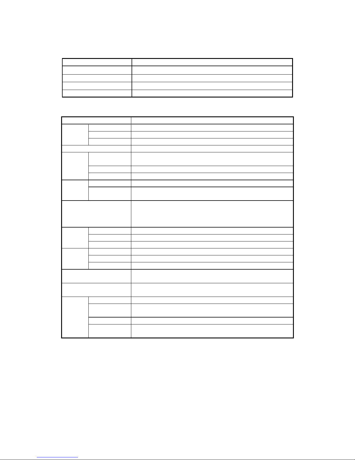
Version List
Version Date Page Modification
1.01 2009.12.24 2 Added HDD Manufacturer’s Parts No.
1.02 2010.1.12 203
149
3
Deleted 5. Flash and Updating BIOS.
Updated Replacement Parts List.
Added Information of Safety Standard and EMI & immunity
1.03 2010.1.21 Cover
4
33
Added (Including HDD SATA Cable x 1).
Added HDD Option.
Added Event Description.
1.04 2010.1.26 118- Modified Disassembly Procedure & Parts List.
1.05 2010.2.1 2 4 Added Windows 7 in Support OS.
Added Dallas Key Reader Unit, Fingerprint Sensor Unit,
Rear Display Unit in Option.
1.06 2010.2.9 35 Added “Note) When application is run on Windows, it is
recommended to calibrate touch panel by Windows Tool.
There is small discrepancy between e-Diag base
adjustment and Windows base adjustment.”
1.07 2010.2.26 149
163
176
Modified Replacement Parts List.
1.08 2010.3.2 135
149
Added New parts.
1.09 2010.4.1 149
150
176
Modified Replacement Parts List.
1.10 2010.5.31 Cover
163
181
Deleted JS-950KT-E10 & JS-950KT-A10, because they are
not fitted to JS-925WS.
Corrected Parts Number.
Added Appendix [JS-925HD-010 Installation Instruction]
1.11 2010.6.9 Cover
2 & 4
186
Added JS-925WS-H50 & JS-925CB-H10
Added JS-925SS-010 Specifications
Added Appendix [JS-925SS-010 Installation Instruction]
1.12 2010.7.1 Cover
9
187
Added JS-925WS-H52
Added Note for Cash Drawer (RJ11 type) Cable.
Added Appendix [RJ type Drawer I/F]
1.13 2010.7.23 92,
93,
94,
98,
101,
109,
115
Corrected Parts List.
1.14 2010.11.5 11-18
4
Cover
Corrected Parts Numbers.
Added comments.
Added JS-950KT-A25/E25

5
CONTENTS
1. Overview ................................................................................................................................................................................................................. 1
1.1. General ............................................................................................................................................................................................................ 1
1.2. Specifications ............................................................................................................................................................................................... 2
1.3. Outside drawing ........................................................................................................................................................................................... 5
1.4. I/O Connectors layout .............................................................................................................................................................................. 6
1.5. Pin Assignment ............................................................................................................................................................................................ 8
1.6. Jumpers ....................................................................................................................................................................................................... 10
2. Description of Operation ............................................................................................................................................................................... 10
2.1. Block Diagram ............................................................................................................................................................................................ 10
2.2. Description of PCB Circuit .................................................................................................................................................................. 11
2.2.1 Main PCB ......................................................................................................................................................................................... 11
2.2.2 Touch Panel PCB ......................................................................................................................................................................... 15
2.2.3 I/O Board ......................................................................................................................................................................................... 16
2.2.4 USB HUB PCB ............................................................................................................................................................................... 18
3. Test Program (eDiag) ..................................................................................................................................................................................... 20
3.1. Initiation method of test program ................................................................................................................................................ 20
3.2. Diagnostic Test Mode ...................................................................................................................................................................... 22
3.2.1. Diagnostic Test Mode Selection ........................................................................................................................................ 22
3.2.2. Diagnostic Test Mode Description. ................................................................................................................................... 22
3.3. Operation mode .................................................................................................................................................................................. 24
3.3.1. Interactive-Administrator mode ......................................................................................................................................... 24
3.3.2. Interactive-User mode ........................................................................................................................................................... 25
3.3.3. Heat run mode ........................................................................................................................................................................... 26
3.4. Diagnosis item ..................................................................................................................................................................................... 28
3.4.1. Random Access Memory Test. ........................................................................................................................................... 28
3.4.2. Hard Disk Test. ......................................................................................................................................................................... 29
3.4.3. Video Test................................................................................................................................................................................... 3 0
3.4.4. Battery Test ............................................................................................................................................................................... 34
3.4.5. Serial Port Test ........................................................................................................................................................................ 36
3.4.6. Customer Display Test ........................................................................................................................................................ 38
3.4.7. System Information Test ...................................................................................................................................................... 39
3.4.8. Touch Panel Test ................................................................................................................................................................... 43
3.4.9. Drawer Test ............................................................................................................................................................................... 47
3.4.10. Ether Test ................................................................................................................................................................................... 50
3.4.11. USB test ...................................................................................................................................................................................... 50
3.4.12. AUDIO TEST .............................................................................................................................................................................. 52
3.4.13. Backlight TEST ......................................................................................................................................................................... 54
3.4.14. i-Button TEST .......................................................................................................................................................................... 55
3.4.15. Finger Print TEST .................................................................................................................................................................... 55
3.5. Message list ......................................................................................................................................................................................... 56
3.5.1. Random Access Memory Test ............................................................................................................................................ 56
3.5.2. Hard Disk Test .......................................................................................................................................................................... 56
3.5.3. Video Test................................................................................................................................................................................... 5 6
3.5.4. Serial port Test ......................................................................................................................................................................... 56
3.5.5. Audio Test ................................................................................................................................................................................. 5 7
3.5.6.
Customer Display Test .......................................................................................................................................................... 57
3.5.7. Touch Panel Test ..................................................................................................................................................................... 57
3.5.8. Drawer Test ............................................................................................................................................................................... 57
3.5.9. Ether Test ................................................................................................................................................................................... 57
3.5.10. USB Test ..................................................................................................................................................................................... 57
3.5.11. Heat Run Test ........................................................................................................................................................................... 57
3.5.12. Input PASSWORD (at entering Interactive Administrator Mode ) ........................................................................ 57
3.5.13. BackLight Test. ......................................................................................................................................................................... 58
4. PCB ........................................................................................................................................................................................................................ 59

6
4.1. Main PCB .................................................................................................................................................................................................... 59
4.1.1. Schematic Diagram ......................................................................................................................................................................... 59
4.1.2. Parts Location .................................................................................................................................................................................. 60
4.1.3. Replacement Parts List ................................................................................................................................................................. 92
4.2. Switch & LED PCB .................................................................................................................................................................................. 96
4.2.1. Schematic Diagram ......................................................................................................................................................................... 96
4.2.2. Parts Location .................................................................................................................................................................................. 97
4.2.3. Replacement Parts List ................................................................................................................................................................. 98
4.3. Touch Panel PCB..................................................................................................................................................................................... 99
4.3.1. Schematic Diagram ......................................................................................................................................................................... 99
4.3.2. Parts Location ................................................................................................................................................................................ 100
4.3.3. Replacement Parts List ............................................................................................................................................................... 101
4.4. JS-925CB-010 Optional I/O PCB ............................................................................................................................................. 102
4.4.1. Schematic Diagram ....................................................................................................................................................................... 102
4.4.2. Parts Location ................................................................................................................................................................................ 103
4.4.3. Replacement Parts List ............................................................................................................................................................... 109
4.5. JS-925HU-010 USB HUB PCB ....................................................................................................................................................... 110
4.5.1. Schematic Diagram ....................................................................................................................................................................... 110
4.5.2. Parts Location ................................................................................................................................................................................ 111
4.5.3. Replacement Parts List ............................................................................................................................................................... 115
5. Cable ................................................................................................................................................................................................................... 116
6. Body Block ........................................................................................................................................................................................................ 118
6.1. JS-925WS-xxx Main Unit. .................................................................................................................................................................. 118
6.1.1. Disassembly Drawing .................................................................................................................................................................... 118
6.1.2. Replacement Parts List ............................................................................................................................................................... 149
6.2. JS-925WS-050/051 LCD Unit. ........................................................................................................................................................ 151
6.2.1. Disassembly Drawing .................................................................................................................................................................... 151
6.2.2. Replacement Parts List ............................................................................................................................................................... 163
6.3. JS-925WS-010 LCD Unit ................................................................................................................................................................... 164
6.3.1. Disassembly Drawing .................................................................................................................................................................... 164
6.3.2. Replacement Parts List ............................................................................................................................................................... 176
7. Trouble Shooting ............................................................................................................................................................................................ 1 7 7
Appendix [JS-925CB-010 Installation Instruction] .............................................................................................................................. 181
Appendix [JS-925HD-010 Installation Instruction] .............................................................................................................................. 186
Appendix [JS-925SS-010 Installation Instruction] ............................................................................................................................... 191
Appendix [RJ type Drawer I/F] ..................................................................................................................................................................... 192
Appendix [AC Cord Kit Installation] ............................................................................................................................................................ 195
Appendix [Cleaning] ........................................................................................................................................................................................... 195
Appendix [Handling] ............................................................................................................................................................................................ 195
Appendix [BIOS Specificaitons] .................................................................................................................................................................... 197

1
1. Overview
1.1. General
JS-925WS was designed for Mid-range.
Main Body was transplanted from JS-790WS.
LCD Unit was transplanted from JS-950WS.
Mother Board was re-designed with new CPU Intel®
ATOM N270 1.6GHz.
For other detail specifications, see the following Specifications.
2
1.2. Specifications
[ Common Specifications ]
Environmental condition
Item Specification
Operating Temperature +5°C – +40°C
Operating Humidity 15% RH – 85% RH (no dew)
Strage Temperature -30°C – +60°C
Strage Humidity 10%RH – 90%RH
[ POS Workstation: JS-925WS-xxx ]
Item Specification
CPU
Type Intel® ATOM N270
Package μFCBGA8
Frequency 1.6GHz
Chip set Intel® 945GSE + ICH 7M
Main
Memory
Capacity
Standard: 1GB (1 SO-DIMM slot)
Maximum: 2GB
Slot 1 DDR-2 SO-DIMM slots, 200pin
Type DDR2-400/533/667
BIOS
Type Flash ROM
BIOS Function
ACPI 1.0b, APM 1.2, PXE boot, USB-FDD boot,
USB-CD ROM/DVD ROM boot, USB Flash Memory boot
Supported OS
Windows XP SP3, WEPOS 1.1 SP3 (nicht unterstützen MFD)
POS Ready 2009, Windows Vista Ultimate, Windows 7
Linux Kernel 2.6
- Unterstützen OPOS
HDD
Type 2.5” (HITACHI HTS545016B9A300)
Size 160GB
I/F SATA (2.5” type)
SSD
Type 2.5” (Transcend TS8GSSD25S-S)
Size 8GB
I/F SATA (2.5” type)
Other Disk Drive (Option)
External USB FDD interface is supported.
External USB DVD/CD-ROM interface is supported.
Local Area Network
Ethernet (10BASE-T/100BASE-TX)
Note : Wake On LAN supported.
Display
Type TFT type LCD with Dual Back Light
Display Size /
Pixel
12.1”: 800x600 (SVGA)
15”: 1024 x 768 (XGA)
Colors 260,000 colors or more
Brightness
12.1”: 400 nits (without touch panel)
15”: 250 nits (without touch panel)

3
Item Specification
Touch
Panel
Type 5-wire resistive
Interface Serial
Life 30 Million touches or more
Surface Non-glare surface treatment
I/O ports
Serial
4 Ports 9pin D-SUB male
- Note: 2 ports are Powered.
Video
1 Port 15pin D-SUB female
- Note: The Dual Display function is supported.
LAN 1 Port RJ-45
USB 2.0
2 USB Ports: IO panel
1 USB Port: Touch Screen unit
1 USB Port: Rear
2 USB Ports: IO panel (Option: JS-925CB)
Audio 1 Port Line-out (Option: JS-925CB)
Cash Drawer
1 Port 6pin modular
1 Port 6pin DIN (Option: JS-925CB)
Expansion I/F
For Communication board: JS-925CB
-IO extension + speaker
Switch
1 Power Switch (Power on / off)
- Hinweis: Rasen Sie on/off, indem Sie eine kurze
Periode schieben.
LED
1 Power (2 Colors: green, red)
Green ON: Power ON
Red ON: Power OFF
1 HDD (green)
Light ON: HDD accessing
1 LAN (green)
Light ON: Send/Receive
Power Supply input AC100V-240V, 50/60 Hz, 1.6A
Size
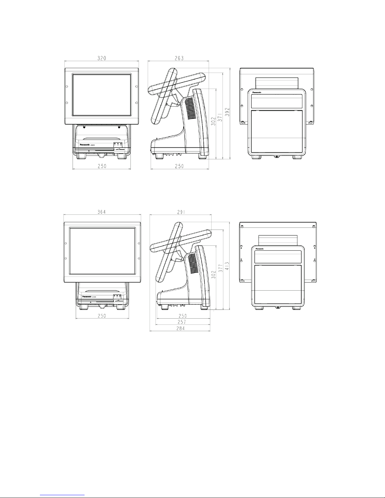
12.1”: Approx. W320mm x D263mm x H392mm
15”: Approx. W364mm x D291mm x H413mm
Carton box: Approx. W514mm x D358mm x H548mm
Mass
Net weight: Approx. 7.57 kg
Gross weight: Approx. 9.18 kg
Standard
Safty cULus, TÜV, CE,GOST, BSMI, SABS
EMI &
immunity
FCC Part15 Class A, ICES-003 Class A, CISPR22 Class A,
CE (EN55022 Class A, EN55024, EN61000), GOST Class A,
BSMI Class A, KCC Class A, C-tick Class A, SABS Class A
4
Item Specification
Option
Communication
board
JS-925CB-010 / JS-925CB-H10
Expansion IO I/F + Speaker
I/F : Expansion I/F
- Line-OUT 1port
- USB 2.0 2ports
- Din type Drawer 1port (Same as JS-950WS)
Note:
The power of +12V, 1A is required to drive DIN type cash
drawer
Carton Box Size: 500mm x 400mm x 270mm
Mass: NET: 1.452Kg GROSS:2.8Kg
HDD Module
JS-925HD-010
Expansion HDD (for Raid) with SATA Cable
Type: 2.5” (HITACHI HTS545016B9A300)
Size: 160GB
I/F: SATA (2.5” type)
USB HUB board
JS-925HU-010
USB-HUB board
Use for 2USB ports of Display unit
Carton Box Size: 500mm x 400mm x 270mm
Mass: NET: 0.906Kg GROSS:2.2Kg
SSD Module
JS-925SS-010
Expansion SSD with SATA Cable
Type: 2.5” (Transcend TS8GSSD25S-S)
Size: 8GB
I/F: SATA (2.5” type)
Backup Battery
(Spare Parts)
Ni-CD: N4HKLNB00007
Ni-MH: BT50024A
Battery Bracket: YJ51-102470
Backup Battery for AC power fail
Note: Retention time: 2 minutes
Battery charge function
Magnetic Card
Reader
JS-950MG-010
Magnetic strip reader module
I/F : USB (Internal connector) Virtual COM
Please see Service Manual MSD0801001C0_JS-950WS for
detail.
Dallas Key
Reader Unit
JS-950DP-010
I/F : USB (Internal connector) Virtual COM
Please see Service Manual MSD0801001C0_JS-950WS for
detail.
Fingerprint
Sensor Unit
JS-950FS-010
I/F : USB (Internal connector) Virtual COM
Please see Service Manual MSD0801001C0_JS-950WS for
detail.
Rear Display
Unit
JS-790RD-010
2 Lines
Please see Service Manual OSSD0600201C0_790WS for
detail.
5
1.3. Outside drawing
12” Touch Screen
15” Touch Screen
6
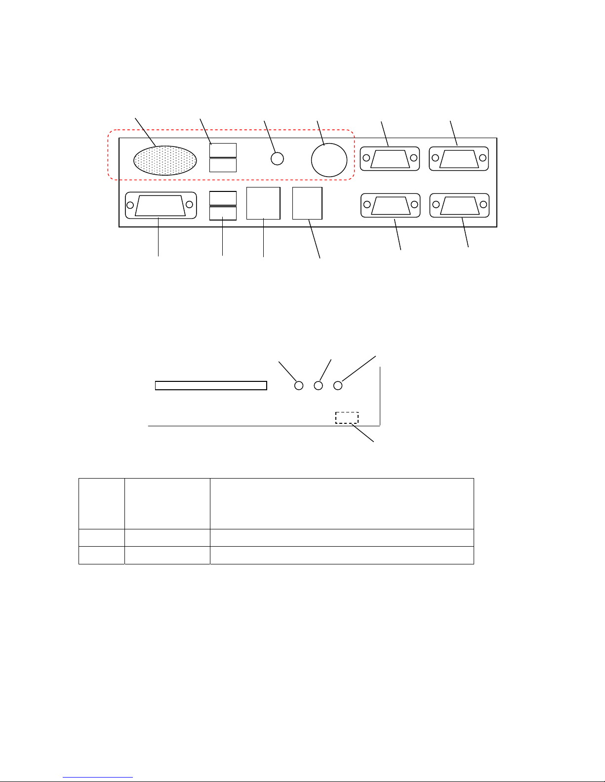
1.4. I/O Connectors layout
(1) Bottom IO Connector layout
(2) Front IO Connector layout SW & LED
LED1 Power State
Shows Power Supply state
Green : Power ON
Red : Soft Off
LED2 LAN Green: The light is on when accessing to LAN
LED3 HDD Green: The light is on when accessing to HDD
○○○○
○○○○○
○○○○
○○○○○
○○○○
○○○○○
○○○○
○○○○○
○○○○
○○○○○
○○○○○
USB#2
USB#1
Ethernet
VGA
USB#3,#4
(Option)
LINE-OUT
(Option)
DIN Drawer#3
(Option)
COM4
COM3
Speaker
(Option)
RJ Drawer#1, #2
COM2
(Powered)
COM1
(Powered)
LAN LED
HDD LED
Power LED
Soft Switch
7
(3) USB Port Positions
USB#8:standard
(Inside of rear cover)
USB#6:standard
For Display unit USB I/F
USB#7:Reserved
(For future use)
USB#5:standard
(Inside of front cover)
USB#3#4:Option
(IO Panel)
USB#1#2:standard
(IO Panel)
8
1.5. Pin Assignment
(1) Ethernet : 8 pin Modular (RJ45)
PIN# Signal PIN# Signal
1 TX+ 5 NC
2 TX- 6 RX-
3 RX+ 7 NC
4 NC 8 NC
(2) USB : USB Connector
PIN# Signal PIN# Signal
1 +5V 3 Data +
2 Data - 4 GND
(3) Powered COM port COM1, COM2 : 9 pin D-SUB Male
PIN# Signal PIN# Signal
1 CD 6 DSR
2 RD 7 RTS
3 TD 8 CTS
4 DTR 9 RI (default) / +5V / +12V
5 GND
・By changing the setting of jumper pins on the PWB, the 9 pin D-SUB can receive either RI(default) or
power supply.
(4) COM port COM3, COM4 : 9 pin D-SUB Male
PIN# Signal PIN# Signal
1 CD 6 DSR
2 RD 7 RTS
3 TD 8 CTS
4 DTR 9 RI
5 GND
(5) Video : 15 pin D-SUB Female
PIN# Signal PIN# Signal PIN# Signal
1 Red 6 GND 11 NC
2 Green 7 GND 12 DCA_DAT
3 Blue 8 GND 13 H-Sync
4 NC 9 VCC 14 V-Sync
5 GND 10 GND 15 DCA_CLK
9
(6) Cash Drawer (DIN type): 6 pin DIN Female
PIN# Signal PIN# Signal
1 Drawer #3 Open 4 GND
2 GND 5 Drawer Type
3 Drawer #3 Status 6 GND
(7) Cash Drawer (RJ type) : 6 pin Modular (RJ11)
PIN# Signal PIN# Signal
1 GND 4 +24V
2 CD #1 Open 5 CD # 2 Open
3 CD # 1 and #2 Status 6 CD # 1 and #2 Status return
NOTE: A special cable is necessary when using 2 drawers concurrently.
“CD #1 & #2 Status” is defined as “Drawer is Opened” when cable is disconnected
or when either cash drawer is opened.
Limitation: Two cash drawers must be connected concurrently in the case a special cable is used,
because “CD #1 and #2 Status” cannot be correct as the actual cash drawer status. In
other words, it’s not acceptable that either one cash drawer is used with a special cable.
Please refer to Appendix F RJ type Drawer I/F
also.
(8) Line-out : Stereo Jack
PIN# Signal PIN# Signal
1 GND 4 NC
2 L_out 5 R_out
3 NC
(9) 2 Lines VFD : COM6 port
PIN# Signal PIN# Signal
1 +5V 5 BUSY(CTS6)
2 +5V 6 GND
3 /RESET 7 GND
4 TxD6
10
1.6. Jumpers
1. JP271 and JP272 Powered COM Setting
No. 9 pin of COM1 & 2 can be changed as follows.
Jumper Setting JP271 for COM1 JP272 formCOM2
1-2 Short +5V +5V
3-4 Short RI (Default) RI (Default)
5-6 Short +12V +12V
2. JP141 Clear CMOS
Jumper Setting
1-2 Short Default
2-3 Short Clear CMOS
11
3. JP371 Battery Charging Voltage Setting
Jumper Setting
1-2 Short For Current Battery (40ohm, Default)
2-3 Short For the future Battery
10
2. Description of Operation
2.1. Block Diagram
LCD
G150XG03V1 (AUO)
Touch Panel
(Higgstec)
DISPLAY
20
20
MAIN
MAIN Board
CN
VFD-2
(COM6)
10Base T or 100Base T
2.5" HDD/SSD
SATA I/F
CN
POW
CN
IO I/F
CN
IO I/F
4
12
12
CN
TP・Inv
(COM5)
20
20
CN
SW-LED
14
14
CN
LVDS
CN
LAN
CN
Analog RGB
CN
USB#1, #2
LCD/
CRT
CN
COM2
CN
COM1
CN
#RJ Drawer 1, #2
CN
#
DIN Drawer 3
JS-750CD etc
Cash Drawer
JS-750CD etc
Cash Drawer
JK401
LINE-OUT
IO Extension Board
CN
COM4
CN
COM3
W2
CN
BAT-IN
Ni-Cd 1200mA/h 7.2V
or
Ni-H
Battery
SO.DIMM
1GB
SPEAKER
Powered
RI/+5V/+12
CN
200
2.5" HDD/SDD
SATA I/F
Communication Board
JS-795CB-010
PSU
85V - 265V
DC OUT
+12V
INLET
W1
FG
φ4
GST3-42R02
.3212-300
(K&B)
L(BROWN)
N(WHITE)
FG(GREEN)
AC Cord
CN
AC IN
1
2
5
C
1
2
5
C
TP-CNT board
CN
CN
15"INV
or
12"INV
CN
CN
CN
4
4
4
4 4
or
4
USB-HUB board
CN
USB#6
4
MSR JIS-1,2 etc
CN
USB#3, #4
CN
SATA I/F
MASTER
W5
W5
OPTION
OPTION
OPTION
CN
SATA I/F
SLAVE
CN
USB#8
7
7
CN
USB#7
CUSTOMER DISPLAY
VFD-2 Lines CU20029-T303C (Noritake)
CN1
CN1
7
7
OPTION
Rear Display Kit
JS-790RD-010
FRONT
SW LED board
Power LED
Green/Red
LED-1
LAN LED
Green
LED-2
HDD LED
Green
LED-3
Power
SW
SW
CN
USB#5
CN
BZ
BZ
D
D D
BUZZER
JS-750CD etc
Cash Drawer
1
2
5
C
Powered
RI/+5V/+12
OPTION
W3
W7-15
or
W7-12
W8
W9
OPTION
OPTION
or
W4
W4
W6-15 or W6-12
11
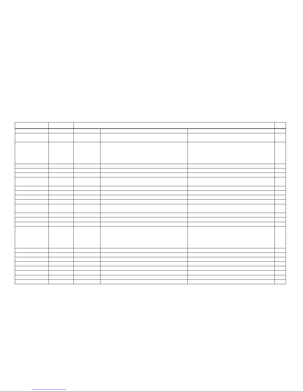
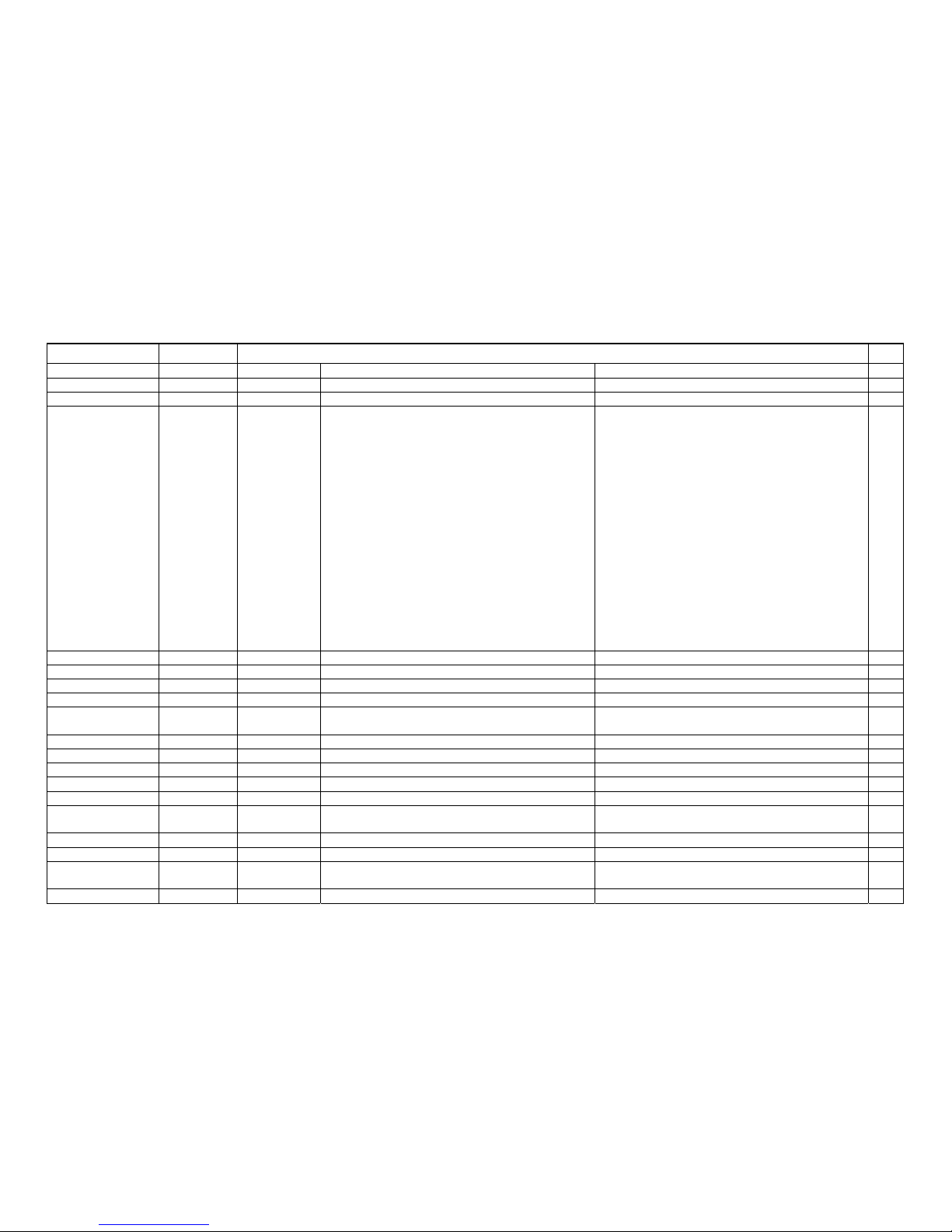
2.2. Description of PCB Circuit
2.2.1 Main PCB
Ref. No. Parts No. Parts Name & Description
Pecs
U051 YJ30-123722 CPU CPU ASIC AU80586GE025D SLB73 C0 FC-BGA8 437P 1
U081 YJ30-123723
Chip Set /
North Bridge
Memory Controller
Video Controller (direct connection to Video I/F)
ASIC QG82945GSE SLB2R A3 FC-BGA3 998P 1
U141 YJ30-122709
Chip Set /
South Bridge
HDD Controller
Drawer Controller (Standard I/O Port)
USB Controller
LAN Controller
Sound Creator
ASIC ICH7-M 82801GBM PFBGA652 1
U152,U342 YJ32-110599S IC SN74AHC1G08DBVR SOT-23 SMT5 2
U162,U163 YJ30-526461S EEPROM 2K 1.8V SO8 AT24C02BN-SH-T 2
U191 YJ32-973876S Clock Clock IC CLOCK ICS9LPRS501PGLFT TSSOP64 L/F 1
U202 YJ30-124167S LAN Controller
LAN Controller
EEPROM for MAC Address and some Parameter
ASIC QFN64 88E8040A0-NNC1C000 MARVELL 1
U211,U365,U369 YJ32-110165S IC CMOS NC7S86P5X_NL SC70 FAIRCHILD LF 3
U214,U302 YJ32-974592S Regulator U214: +24V Regulator for Cash Drawer IC CONTROLLER TPS40211DGQR MSOP10 2
U221,U222 YJ32-191308S IC CMOS SN74LVC1G125DBVR SOT23-5 2
U225 YJ32-973604S IC VOLTAGE TRANSLATOR PCA9306 VSSOP8 1
U241,U242,U243,
U244
YJ38-970001S IC TVS D ARRAY NUP4201MR6T1G TSOP6 W/LF 4
U251 YJ32-975388S Regulator +1.2V Regulator for HDD Controller (U253) Regulator RT9166A-12PGL 1.2V SOT-223 1
U252 YJ30-124166S HDD Controller HDD Controller ASIC IC 88SE6121B2-NAA2C000 QFN76 1
U261 YJ30-123324S Super I/O Serial Controller for COM1-4, TP & Customer Display IC ASIC LPC I/O QFP128 W83627UHG REV:B 1
U271
U272
U281
U291
U292
YJ32-970073S Transceiver
U271: COM1 Transceiver
U272: COM2 Transceiver
U281: TP Transceiver
U291: COM3 Transceiver
U292: COM4 Transceiver
IC MAX3243ECPWR TSSOP28 5
U293 YJ32-110015S IC LMOS TC7S32FU(TE85L,F) SSOP5-P-A LF 1
U301 YJ32-972165S IC REGULATOR G905T24Uf 2.5V SOT-89 GMT 1
U313 YJ32-975361S Regulator +3.3V Regulator (3.3V is created from +5V) IC CONTROLLER PM6686TR VFQFPN-32 1
U321 YJ32-974651S Regulator +1.8V Regulator for Memory IC CONTROLLER ISL8014IRZ-T QFN 16 1
U322 YJ32-974653S Regulator +0.9V Regulator for Memory Terminator IC REGULATOR TPS51200DRCR SON-10 1
U331,U332 YJ32-974282S Regulator U332: +1.05V Regulator for Chip Set / CPU I/F BUS IC BUCK CONTROLLER NCP1589AMNTWG DFN10 2
U341 YJ32-974996S Regulator V Core Regulator for CPU IC ADP3211AMNR2G QFN32 1
U361 YJ32-110185S IC CMOS 74LVC08D SO14 PHILIPS 1
12
Ref. No. Parts No. Parts Name & Description
Pecs
U362 YJ32-974660S IC ADM1815-R23ARTZ-RL SOT-23 1
U372,U373 YJ32-971543S IC MIC841HYC5 SC70-5 (LF) 2
Q161 YJ35-950028S TR DUAL FFB3904 SC70-6 FAIRCHILD 1
Q162,Q163,Q211,
Q214,Q216,Q222,
Q223,Q241,Q242,
Q243,Q244,Q245,
Q246,Q247,Q248,
Q302,Q303,Q305,
Q308,Q331,Q333,
Q334,Q336,Q337,
Q338,Q351,Q352,
Q353,Q354,Q355,
Q356,Q357,Q358,
Q359,Q362,Q367,
Q376,Q377,Q2611,
Q2612,Q2613,Q2614,
Q3010,Q3012,Q3013,
Q3014,Q3015,Q3510,
Q3710,Q3711,Q3511,
Q3512
YJ35-339001S MOSFET TR 2N7002 SOT-23 FAIRCHILD 52
Q164 YJ35-220018S PNP TR MMBT3906LT1G SOT23 ON-SEMI L/F 1
Q215,Q332,Q341 YJ35-390614S Transistor Q332: 1.5V Regulator for Chip Set Core TR FET DULE N CHANNEL FDS6982AS SO8 3
Q217 YJ35-390502S Regulator +24V Regulator for Cash Drawer TR N-CHANNEL MOSFET FDS8896 SO-8 1
Q221 YJ35-339215S TR FET P-CHANNEL APM2301AAC SOT-23 1
Q301,Q306,Q309,
Q371,Q379
YJ35-390580S FET Q371: FET for ??? TR MOSFET P-CHANNEL FDS4435BZ SO-8 5
Q3011 YJ35-391734S TR MOSFET N-CHANNEL STD60N3LH5 DPAK 1
Q304 YJ35-100066S TR NPN DTC143ZUA-T106 SC-70(UMT3) 1
Q307 YJ35-390130S TR FET P-CHANNEL FDC604P_NL SSOT-6 1
Q311,Q312,Q335 YJ35-900014S Regulator Q311: +5V Regulator TR FET DUAL N-CHANNEL FDMS9600S POWER56 3
Q343 YJ35-110034S NPN TR MMBT3904 SOT23 1
Q361,Q363,Q364,
Q365,Q366,Q374
YJ35-229032S PNP DIGITAL TR DTA123JUA SC-70 ROHM 6
Y141 YJ44-300338S X'TAL 32.768KHz 20PPM 12.5PF SMD4P 1
Y191 YJ44-345663S X'TAL 14.31818M 30PPM 20PF SMD DSX630G 1
Y201
Y251
YJ44-345770S Chrystal
Y201: 25MHz for LAN Controller (U202)
Y251: 25MHz for HDD Controller (U253)
X'TAL 25MHZ 30PPM 20PF SMD 1HG25000CC1J 2
BIOSFLASH YJ30-515749S FMEM 16MBIT SPI SERIAL 2.7-3.6V SO8 SST 1
13
U252
U271
U272
U281
U321
U332
U341
Q332
Q
217
Q371
Q311
+24V for Cash Drawer generation area
+5V generation area
+3.3V
generation
area
+1.5V for Chipset Core generation area
U191
+1.8V for Memory generation area
14
U214
U291
U292
+1.5V generation area
+0.9V for Memory
Terminator
generation area

15
2.2.2 Touch Panel PCB
Ref. No. Parts No. Parts Name & Description
Pcs/set
U13 YJ30-123189
TP
Controller TP Controller ASIC MCU 16K F/W:1.08.D2-AI MLP-28 1
U14,U15,U24 YJ35-390351S TR FET P-CHANNEL SI1555DL-T1-E3 SOT-363 3
U43 YJ30-526683S EEPROM 4K AF93BC66-SI SOIC8 APLUSFLASH 1
U44 YJ32-300015S Transceiver RS-232C Transceiver IC RS-232 TRANSCEIVER SO16 SP202EEN 1
Q8 YJ32-974712S Regulator Regulator for RS-232C LDO REGULATOR ad 3A GS1085LDF TO-252 1
U44
Q8
16
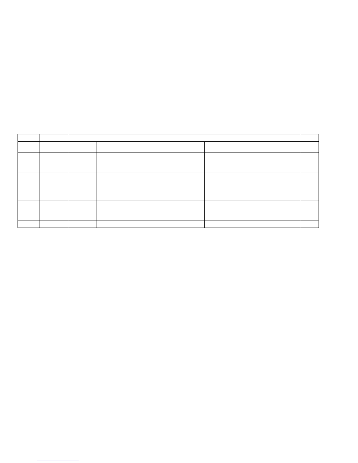
2.2.3 I/O Board
Ref. No. Parts No. Parts Name & Description
Pcs/set
U1 YJ32-960258S Regulator
+5V Regulator for Audio Codec (U2) (+5V is created from
+12V)
IC REGUALTOR MC78M05CDTRKG DPAK-3 1
U2 YJ30-123256S Audio Codec Audio Codec (Sound Output) ASIC ALC662-GR LQFP48 REALTEK 1
U3 YJ38-950121S IC TVS D ARRAY NUP4102XV6T1G SOT563 1
U4 YJ32-970523S Audio AMP Audio AMP IC AMPLIFIER BD7830NUV-TR VSON008V2030 1
U5 YJ38-970001S IC TVS D ARRAY NUP4201MR6T1G TSOP6 W/LF 1
U6 YJ32-110165S IC CMOS NC7S86P5X_NL SC70 FAIRCHILD LF 1
U7 YJ32-191129S
Drawer
Timing
Controller
Drawer Timing Controller IC SN74LV123APWT TSSOP16 L/F 1
Q1,Q5,Q6 YJ35-339001S MOSFET TR 2N7002 SOT-23 FAIRCHILD 3
Q2 YJ35-100066S TR NPN DTC143ZUA-T106 SC-70(UMT3) 1
Q3 YJ35-390580S TR MOSFET P-CHANNEL FDS4435BZ SO-8 1
Q4 YJ35-220018S TR PNP MMBT3906 SOT23 PHILIPS 1
17
U1
U2
Audio AMP area
18
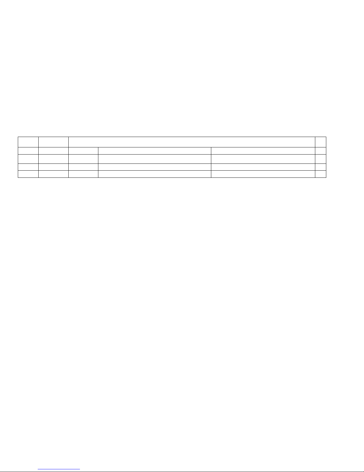
2.2.4 USB HUB PCB
Ref.
No.
Parts No. Parts Name & Description
Pcs
U1 YJ38-950088S D ARRAY DVIULC6-4SC6 SOT23-6L ST 1
U7 YJ30-123603S
HUB
Controller HUB Controller IC USB HUB CONTROLLER QFN36 USB2512-AEZG 1
Q8 YJ32-974712S Regulator Regulator for HUB Controller (U1) (?V is created from +5V) LDO REGULATOR ad 3A GS1085LDF TO-252 1
Y3 YJ44-345600S Crystal Clock for HUB Controller X'TAL 24MHZ 20PPM 18PF SMD4 7B24000065 1
19
U7
Q8
Y3
20
3. Test Program (eDiag)
3.1. Initiation method of test program
Before executing e-Diag, please make sure the setting of ATA/IDE configuration is “Compatible Mode”.
If not, please enter the BIOS Advanced Page and change the setting of ATA/IDE configuration from
“Enhanced Mode” to “Compatible Mode”.
Initiation method of ROM version 925ROM
1. Keyboard start
The USB keyboard is connected with JS-925, and the power supply is turned on. The [F10] Insert
key is
pressed while POST.
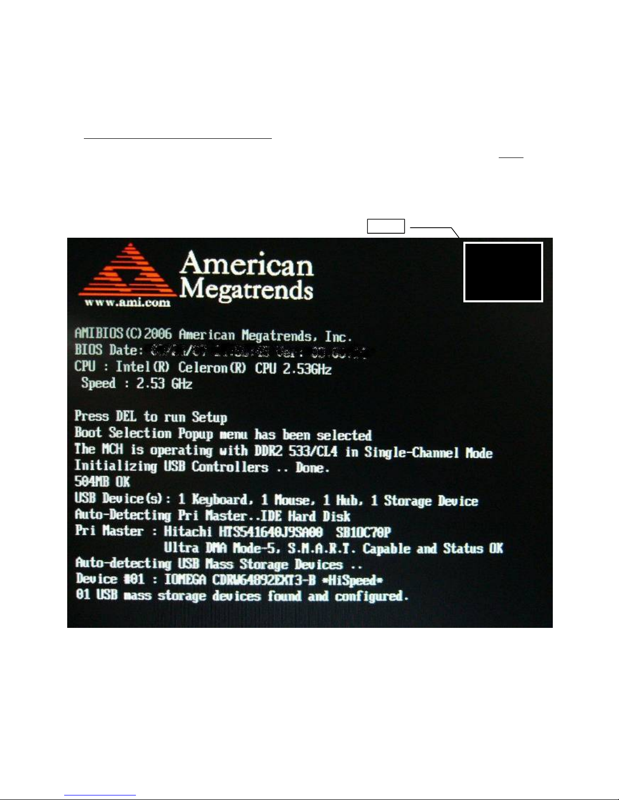
2. Touch panel start
The power supply of JS-925 is turned on. It touches a square button on the right top of the screen while
counting the memory of POST.
Screen of LCD
3. Automatically start
¾
When system boots up, BIOS read and check CMOS data, which is set as “Launch Diagnostic program”, so
BIOS automatically launch the diagnostic program.
¾
When Diagnostic protram starts, it read and check COMS data to understand which mode (Auntomatically or
not) should be executed.
¾
If CMOS data is set as “Automatically”, diagnostic program have to check the CMOS data what tests should
be executed. In other words, changing CMOS data can select the test item in Auntomatic Mode.
Please refer to BIOS specification document to know better about work low
Here
======
======
======

21
at “Diag. 3-1 Workflow”,
“Table 3-1 Option Feature List and Operation Method” and
“Diag. 3-7 Diagnostic program (Workflow)
Initiation method of DISK version 925DISK
4. Start from MS-DOS prompt
The power supply of JS-925 is turned on. If the prompt of MS-DOS is displayed, it is input as "
925DISK.EXE ".
- MS-DOS is assumed to be Ver6.22.
22
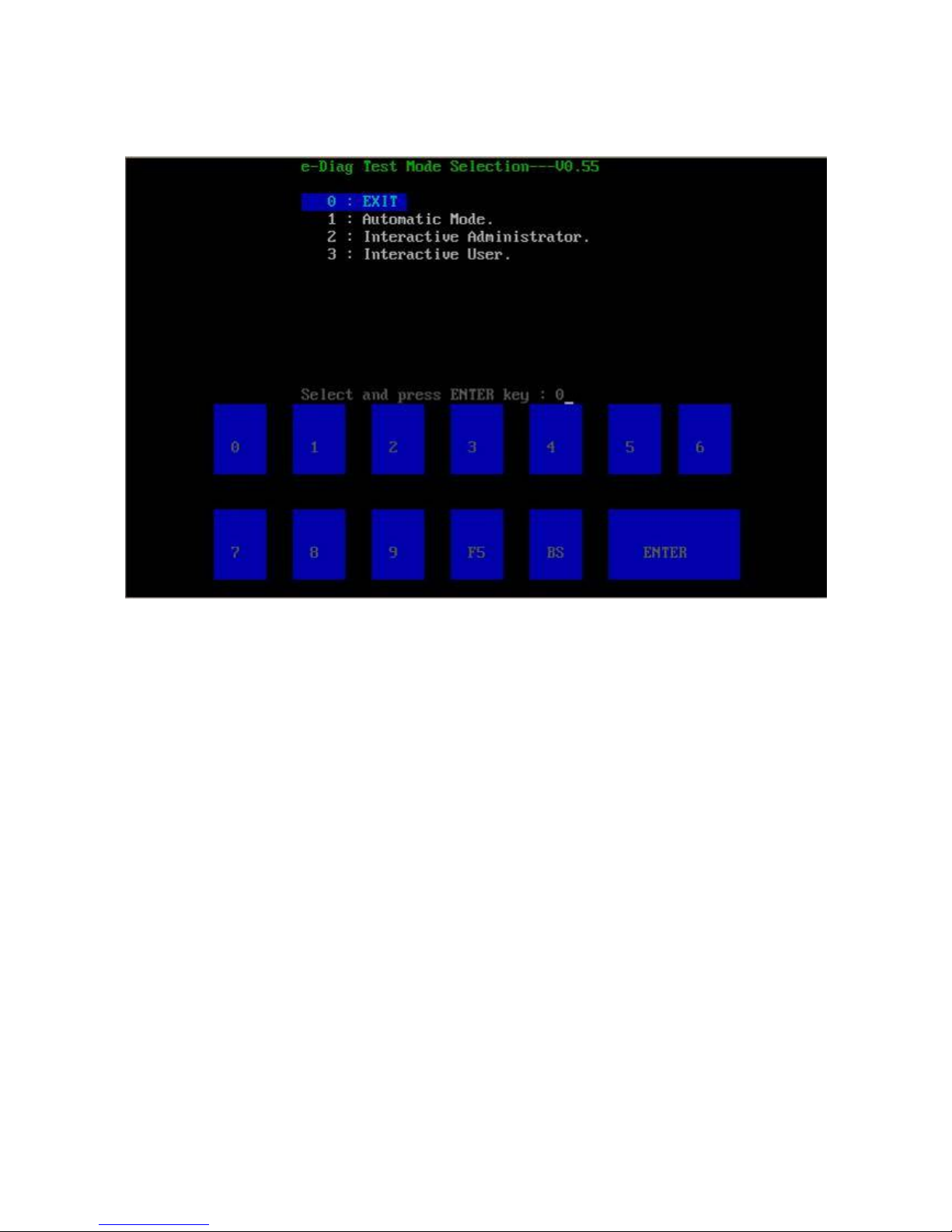
3.2. Diagnostic Test Mode
3.2.1. Diagnostic Test Mode Selection
The Diagnostic test mode can be selected in Diagnostic test mode selection page of the BIOS Setup
Manager. Reference the following Figure 4-1.
Figure 4-1 Diagnostic Test Mode Selection
3.2.2. Diagnostic Test Mode Description.
1. Interactive Administration Mode Description:
If user selected the Interactive Administration mode (restricted by password) in Diagnostic test mode
selection page, user can select to run a test item from all test items individually after inputting password as the
following figure.
Note: When the user wants to run the Diagnostic Test Program in Interactive Administrator mode, he must
enter the Administration Password correctly.
 Loading...