

Panasonic JS-170FR-U20, JS-170FR-U21, JS-170FR-U22, JS-170FR-U24, JS-170FR-U23 Service Manual
...
ORDER NO.ISD0110009S0
G20
Service M a n u a l
Front Counter Register
JS-170FR-**
© 2001 Matsusita Comm uni cation Industrial Co., Ltd.
All right reserved. Unauthorized copying and
distribution is a violat ion of law.

WARNING
This service inform ation i s des igned f or experienced repair tec hnic ians only and is not designed f or us e
by the general public. It does not contain warnings or cautions to advise non-technical should be
potential dangers in attempting to service a product. Products powered by electricity should be
serviced or repaired only by experienced professional technic ians. Any at temp t to servic e or repair t he
product or products dealt with in t his service information by anyone c ould result in serious injury or
death.
Design and specificati ons are subject to change without notice.
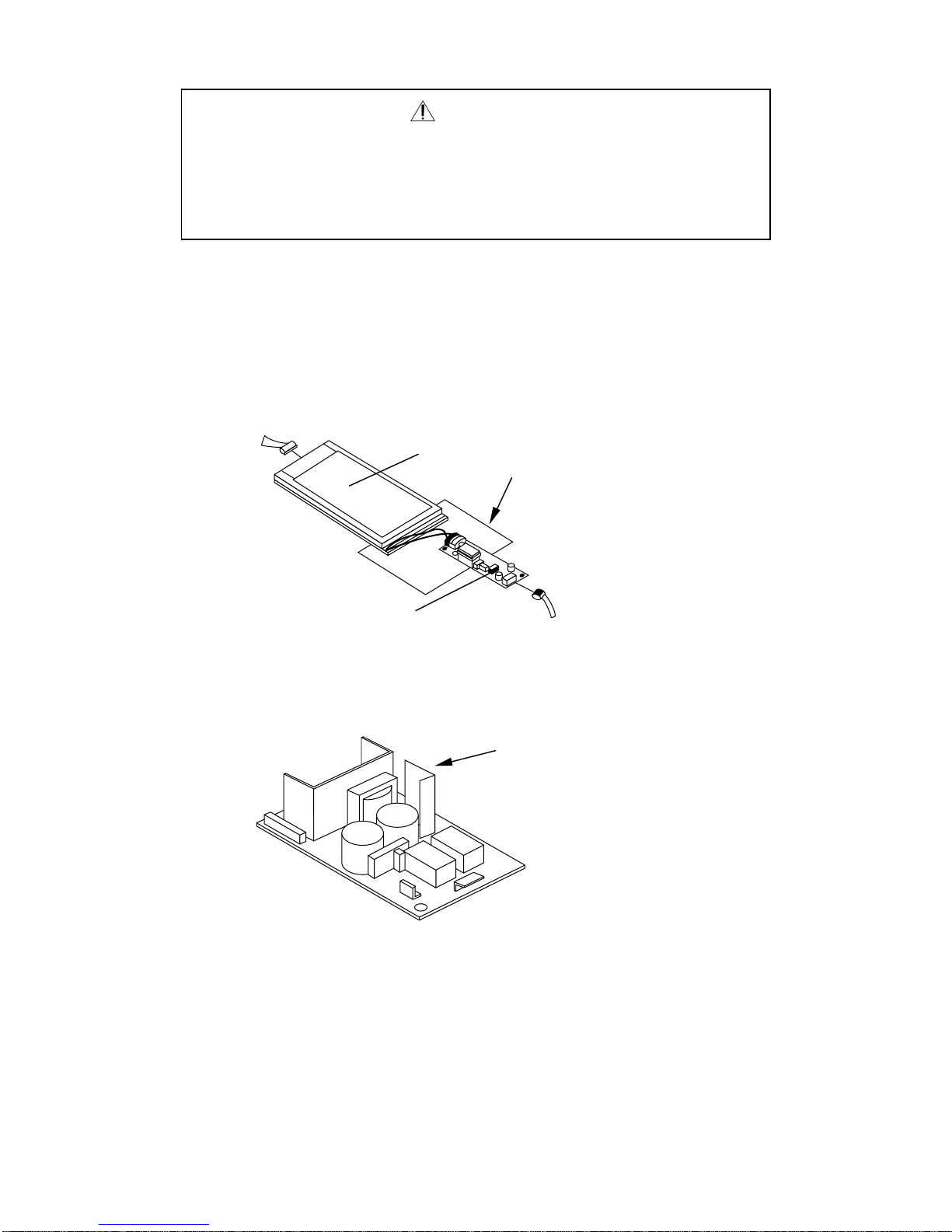
Caution
(1) High voltage is applied to inverter t ransformer, cable and capacit or on the backli ght PCB and back light connec tor shown i n
Fig. 1 below.
Do not touch those parts without switc hing off JS-170FR, expect f or probes of osc illoscope or tester for test ing or repairing
purpose only.
Fig.1
LCD Unit
Do not touch the parts within this spot,
without switching off JS-170FR
Backlight PCB Assy
(2) High voltage (230 V DC) is applied to heat sink (indicated by arrow) on Power Supply PCB Unit shown in the Fi gure bel ow.
Do not touch this part without switching off JS-170FR
Do not touch the parts within this spot,
without switching off JS-170FR
Power Supply PCB Unit
Design and specificati ons are subject to change without notice.
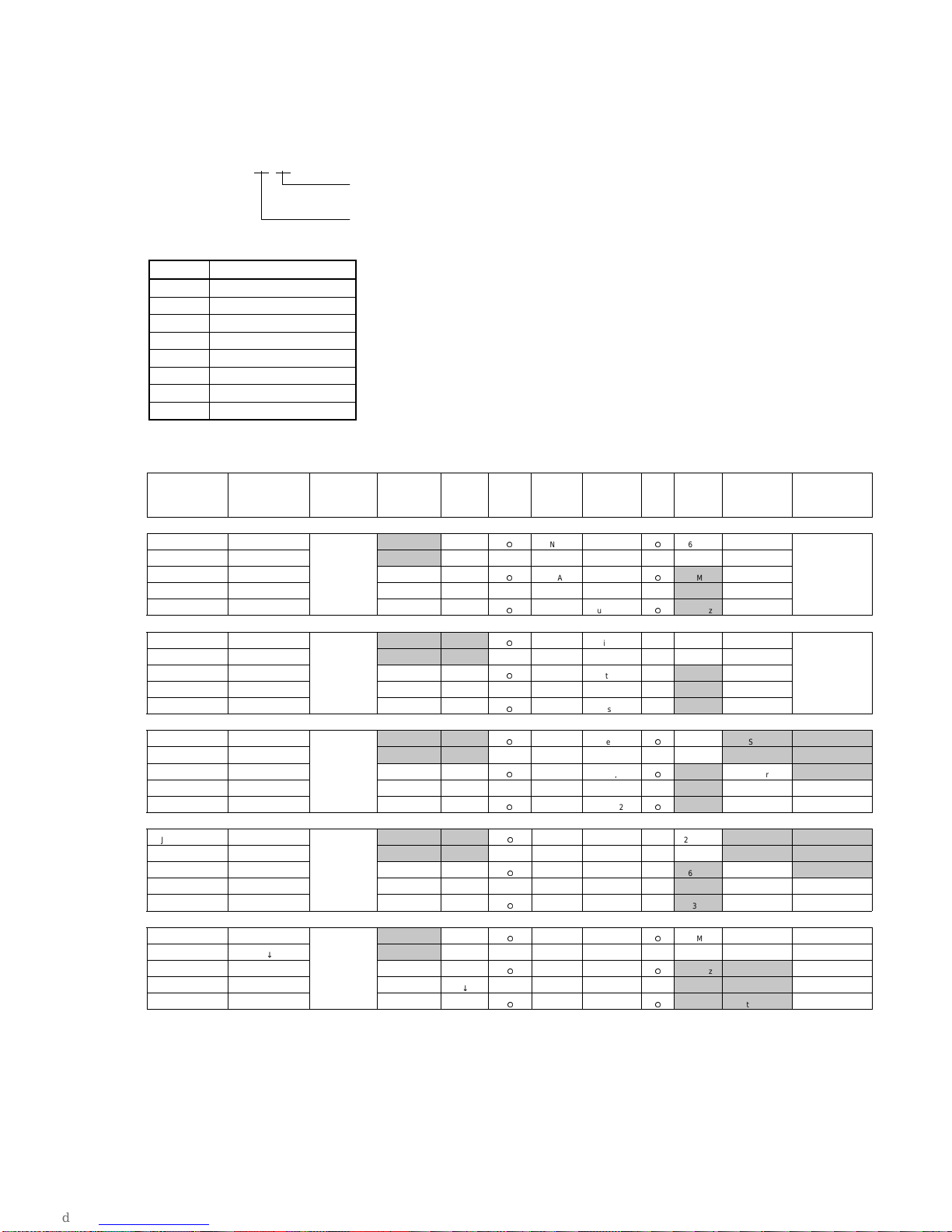
International Pentium P O S Series Models are classifi ed according to the system s shown below.
JS-170FR-X1, X2
Type of Specifications
Country Code
X1 Country Code
Code Country or Area
E England
GGermany
F European
A Australia
WTaiwan
U U.S.A, Canda
S Scandinavia
C Canada
Type of JS-170FR Specifications
Model No.
Specification
change timing
Country Cap Col or
RAM size
(MB)
Battery O/S
(TP, MSR)
Dip SW
Customer
Display
CPU MSR Other
JS-170FR-U20 From begin Yellow 64
↓↓ ↓↓↓↓↓↓↓ ↓
JS-170FR-U22 June,2001 Gray 64
↓↓ ↓↓↓↓↓↓↓↓
JS-170FR-U24 September,2001
JS-170FR-U21 From begin Yellow 64
↓↓ ↓ ↓↓↓ ↓↓↓ ↓
JS-170FR-U23 June,2001 Gray 64
↓↓ ↓↓↓↓↓↓↓↓
JS-170FR-U25 September,2001
JS-170FR-G20 From begin Yellow 16
↓↓ ↓ ↓↓↓ ↓↓↓ ↓ ↓
JS-170FR-G22 July,2001 Friendly Gray 64
↓↓ ↓↓↓↓↓↓↓↓
JS-170FR-G24 September,2001
JS-170FR-G21 From begin Yellow 16
↓↓ ↓ ↓↓ ↓↓↓ ↓ ↓
JS-170FR-G23 July,2001 Friendly Gray 64
↓↓ ↓↓↓ ↓↓↓↓
JS-170FR-G25 September,2001
JS-170FR-E20 From begin Yellow 64
↓↓ ↓↓↓↓↓↓↓ ↓
JS-170FR-E22 June,2001 Gray 64
↓↓ ↓↓↓↓↓↓↓ ↓
JS-170FR-E24 September,2001
USA
Gray 64
USA
Gray 64
Germany
Friendly Gray 64
Germany
Friendly Gray 64
UK
Gray 64
{
{
{
{
{
{
{
DOS 6.22 Gen, 2
{
DOS 6.22 Gen, 2
{
DOS 6.22 Gen, 2
{
DOS 6.22 Gen, 2
{
DOS 6.22 Gen, 2
{
DOS 6.22 Gen, 2
{
{
{
N/A Fujitsu, 1/2
N/A Fujitsu, 1/2
N/A Fujitsu, 1/2
N/A Fujitsu, 1/2
N/A Fujitsu, 1/2
N/A Fujitsu, 1/2
N/A Fujitsu, 1/2
N/A Fujitsu, 1/2
N/A Fujitsu, 1/2
{
266MHz Not Standard
{
266MHz Not Standard 120V
{
333MHz Not Standard
×
266MHz Not Standard
×
266MHz Not Standard 120V
×
333MHz Not Standard
{
266MHz Not Standard AC Cable Straight
{
266MHz Standard AC Cable L type
{
333MHz Standard
×
266MHz Not Standard AC Cable Straight
×
266MHz Standard AC Cable L type
×
333MHz Standard
{
266MHz Not Standard
{
266MHz Not Standard
{
333MHz Standard

Model No.
JS-170FR-E21 From begin Yellow 64
↓↓ ↓↓↓↓↓↓↓ ↓
JS-170FR-E23 June,2001 Gray 64
↓↓ ↓↓↓↓↓↓↓ ↓
JS-170FR-E25 September,2001
Specification
change timing
Country Cap Col or
UK
Gray 64
RAM size
(MB)
Battery O/S
{
N/A Fujitsu, 1/2
{
N/A Fujitsu, 1/2
{
N/A Fujitsu, 1/2
(TP, MSR)
Dip SW
Customer
Display
×
266MHz Not Standard
×
266MHz Not Standard
×
333MHz Standard
CPU MSR Other
JS-170FR-S20 From begin Yellow 64
↓↓ ↓ ↓ ↓↓ ↓↓↓↓
Discontinue June,2001
JS-170FR-F22 June,2001 Gray 64
↓↓ ↓↓↓↓↓↓↓ ↓
JS-170FR-F24 September,2001
JS-170FR-F23 June,2001 Gray 64
↓↓ ↓↓↓↓↓↓↓ ↓
JS-170FR-F25 September,2001
JS-170FR-A20 From begin Yellow 16
↓↓ ↓ ↓↓↓ ↓↓↓ ↓
JS-170FR-A22 June,2001 Gray 64
↓↓ ↓↓↓↓↓↓↓ ↓
JS-170FR-A24 September,2001
JS-170FR-A23 June,2001 Gray 64
↓↓ ↓↓↓↓↓↓↓ ↓
JS-170FR-A25 September,2001
JS-170FR-W20 From begin Yellow 16
↓↓ ↓ ↓↓↓ ↓↓↓ ↓
JS-170FR-W22 June,2001 Gray 64
↓↓ ↓↓↓↓↓↓↓ ↓
JS-170FR-W24 September,2001
Scandinavia
N/A N/A N/A N/A N/A N/A N/A N/A
European
Gray 64
European
Gray 64
Australia
Gray 64
Australia
Gray 64
Tai wan
Gray 64
{
{
{
{
{
{
DOS 6.22 Gen, 2
{
{
{
{
{
DOS 6.22 Gen, 2
{
{
Fujitsu, 1/2
N/A
N/A Fujitsu, 1/2
N/A Fujitsu, 1/2
N/A Fujitsu, 1/2
N/A Fujitsu, 1/2
N/A Fujitsu, 1/2
N/A Fujitsu, 1/2
N/A Fujitsu, 1/2
N/A Fujitsu, 1/2
N/A Fujitsu, 1/2
N/A Fujitsu, 1/2
{
266MHz Not Standard
{
266MHz Not Standard
{
333MHz Standard
×
266MHz Not Standard
×
333MHz Standard
{
266MHz Not Standard
{
266MHz Not Standard
{
333MHz Standard
×
266MHz Not Standard
×
333MHz Standard
{
266MHz Not Standard
{
266MHz Not Standard 120V
{
333MHz Standard
AC Cable L type
AC Cable L type
JS-170FR-W23 June,2001 Gray 64
↓↓ ↓↓↓↓↓↓↓ ↓
JS-170FR-W25 September,2001
JS-170FR-C24 April,2002 Canada Gray 64
JS-170FR-C25 April,2002 Canada Gray 64
Tai wan
Gray 64
{
{
{
{
N/A Fujitsu, 1/2
N/A Fujitsu, 1/2
N/A Fujitsu, 1/2
N/A Fujitsu, 1/2
×
266MHz Not Standard
×
333MHz Standard
{
333MHz Standard 120V
×
333MHz Standard 120V
120V
Serial Number Control Table for Classified Modifications in the JR-170FR Models
Model Number
#
Modification Description U20,U21 U22,U23 U24,U25 G20,G21 G22,G23 G24,G25 E20,E21 E22,E23 E24,E25 S20,21
1
Main board modified
2
Resistor R430 added 10 kilo-ohms added 01A***** -------- -------- 01A***** -------- -------- 01A***** -------- -------- 01A*****
Constant of resistor
3
R181 modified
4
DIMM enhanced From 16 MB to 64 MB 01B***** -------- -------- 01B***** -------- -------- 01B***** -------- -------- 01B*****
Baud rate of customer
5
display enhanced
6
Operating System
7
Power supply modified Manufacturer changed 01D***** -------- -------- 01D***** -------- -------- 01D***** -------- -------- 01D*****
8
Power supply modified Diffuser panel added -------- -------- 02A***** -------- -------- 02A***** -------- -------- 02A***** --------
9
CN1 Not implemente d 01 D***** -------- -------- 01D***** -------- -------- 01D***** -------- -------- 01D*****
10
IDE interface buffer
LAN LSI driver
11
software version-up
12
Hard disk enhanced From 3.25 GB to 5 GB -------- 01F***** -------- -------- 01F***** -------- -------- 01F***** -------- --------
13
LAN driver software Software modified -------- 01J***** -------- -------- 01J***** -------- -------- 01J***** -------- --------
R430 jumper wire
imbedded
From 1.2 kilo-ohms to
750 ohms
From 2400 bps to 9600
bps (except G version)
Not pre-installed
(except G version)
IC18-23 not
implemented
LSI manufacturer
demand
01D***** -------- -------- 01D***** -------- -------- 01D***** -------- -------- 01D*****
01A***** -------- -------- 01A***** -------- -------- 01A***** -------- -------- 01A*****
01B***** -------- -------- 01B***** -------- -------- 01B***** -------- -------- 01B*****
01B***** -------- -------- 01B***** -------- -------- 01B***** -------- -------- 01B*****
01D***** -------- -------- 01D***** -------- -------- 01D***** -------- -------- 01D*****
-------- 01J***** -------- -------- 01J***** -------- -------- 01J***** -------- --------
Lower case modified
14
(1)
Lower case modified
15
(2)
Battery replacement
simplified
Rubber foot frame
reinforced
00N***** -------- -------- 00H***** -------- -------- 00F***** -------- -------- 00N*****
-------- -------- 02B***** -------- -------- 02B***** -------- -------- 02B***** --------
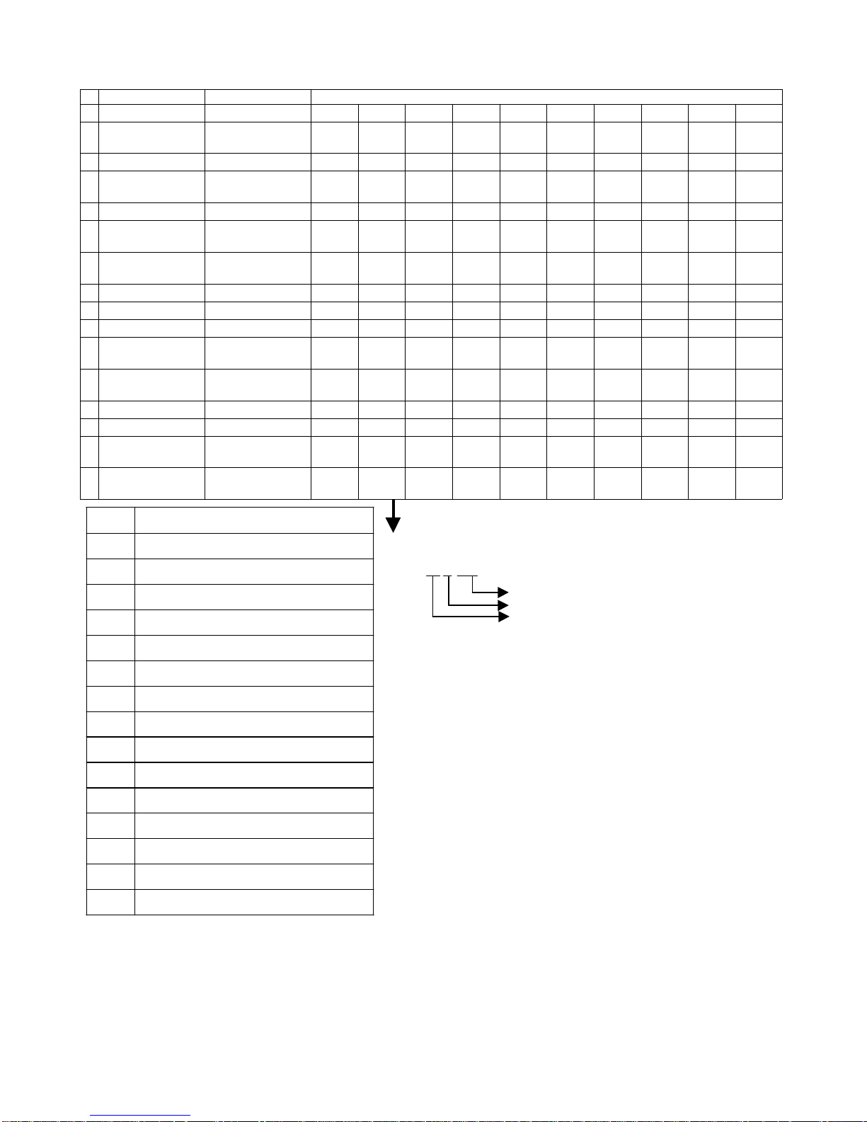
Model Number
# Modification Description F22,F23 F24,F25 A20,A21 A22,A23 A24,A25
Main board modified
1
2 Resistor R430 added 10 kilo-ohms added -------- -------- 01A***** -------- -------- 01A***** -------- -------- --------
Constant of resistor
3
R181 modified
4 DIMM enhanced From 16 MB to 64 MB -------- -------- 01B***** -------- -------- 01B***** -------- -------- --------
Baud rate of customer
5
display enhanced
Operating System
6
7 Power supply modified Manufacturer changed -------- -------- 01D***** -------- -------- 01D***** -------- -------- -------8 Power supply modified Diffuser panel added -------- 02A***** -------- -------- 02A***** -------- -------- 02A***** 02A*****
9 CN1 Not implemented -------- -------- 01D***** -------- -------- 01D***** -------- -------- --------
IDE interface buffer
10
LAN LSI driver
11
software version-up
12 Hard disk enhanced From 3.25 GB to 5 GB 01F***** -------- -------- 01F***** -------- -------- 01F***** -------- -------13 LAN driver s oftware Software modified 01J***** -------- -------- 01J***** -------- -------- 01J***** -------- --------
Lower case modified
14
(1)
Lower case modified
15
(2)
Modifica-
tion No.
1 R430 jumper wire imbedded
Measures against locking up during LAN
2
communication
3 Brightened CRT connected to VGA output
4 User demand
5 User demand
6 User demand
7 Attainment of stable parts supplier
8 Holding down temperature rise of stainless case
9 Elimination of connector for debugging
R430 jumper wire
imbedded
From 1.2 kilo-ohms to
750 ohms
From 2400 bps to 9600
bps (except G version)
Not pre-installed
(except G version)
IC18-23 not
implemented
LSI manufacturer
demand
Battery replacement
simplified
Rubber foot frame
reinforced
Reason for modification
-------- --------
-------- --------
-------- --------
-------- --------
-------- --------
01J***** --------
-------- --------
-------- 02B***** -------- -------- 02B***** -------- -------- 02B***** 02B*****
01D*****
01A*****
01B*****
01B*****
01D*****
--------
00F*****
• How to read serial numbers (starting month of modifying the specifications)
Ex.)
Example) 02 A *****
-------- --------
-------- --------
-------- --------
-------- --------
-------- --------
01J***** --------
-------- --------
W 20,W21 W 22,W23 W 24,W 25
01D*****
01A*****
01B*****
01B*****
01D*****
--------
00A*****
Production number
Production month (A = January) A = January
Production year (2002) B = February
-------- -------- --------
-------- -------- --------
-------- -------- --------
-------- -------- --------
-------- -------- --------
01J***** -------- --------
-------- -------- --------
C24,C25
C = March
D = April
E = May
F = June
H = July
J = August
K = September
L = October
M = November
N = December
10 Elimination of Ultra DMA trouble
11 Ceased production of the part
12 Better marketability
13 TP slowdown
14 User demand
15 Prevention of rubber foot frame from being broken

CONTENTS
1 OVERVIEW................................................................................................................................................1-1
General ........................................................................................................................................................1-1
System Configurations (Example)................................................................................................................1-1
Specifications...............................................................................................................................................1-2
Memory Map ................................................................................................................................................1-6
I/O Port Map.................................................................................................................................................1-7
Interrupt Level ..............................................................................................................................................1-8
Pin assignments...........................................................................................................................................1-9
Appendix B : Dip Switches and Jumpers ...................................................................................................1-16
2 Description of Operation ............................................................................................................................ 2-1
JS-170FR Block Diagram ............................................................................................................................2-1
Description of Main PCB Circuits.................................................................................................................2-2
2.1.1 CPU PENTIUM-II 266MHz or 333MHz (Refer to the page 4-1.) ................................................2-2
2.1.2 Chip set FW82443BX, FW82371EB (Refer to the page 4-1 and page 4-3.)..............................2-2
2.1.2.1 FW82371EB Pin Assignment ..................................................................................................2-3
2.1.2.2 RTC (Real Time Clock) circuit.................................................................................................2-9
2.1.2.3 IDE interface..........................................................................................................................2-10
2.1.2.4 USB interface.........................................................................................................................2-12
2.1.3 Main RAM circuit.......................................................................................................................2-13
2.1.4 BIOS ROM................................................................................................................................2-14
2.1.5 IT8673F circuit..........................................................................................................................2-15
2.1.5.1 IT8673F Pin Assignment.......................................................................................................2-16
2.1.5.2 Serial port (COM1, 2).............................................................................................................2-18
2.1.5.3 Parallel port interface circuit ..................................................................................................2-20
2.1.5.4 FDD interface circuit..............................................................................................................2-21
2.1.5.5 Keyboard controller circuit .....................................................................................................2-23
2.1.5.6 PS/2 mouse controller circuit.................................................................................................2-25
2.1.6 Serial port (COM3, 4)................................................................................................................2-26
2.1.7 VGA circuit (Refer to the page 4-4.).........................................................................................2-28
2.1.7.1 SM710 Pin Assignment .........................................................................................................2-29
2.1.7.2 LCD interface circuit (Refer to the page 4-4.)........................................................................2-33
2.1.7.3 Back-Lite control circuit .........................................................................................................2-34
2.1.7.4 CRT interface ........................................................................................................................2-35
2.1.8 Piezoelectric buzzer circuit .......................................................................................................2-36
2.1.9 Hardware reset circuit...............................................................................................................2-37
2.1.10 Clock.........................................................................................................................................2-38

2.1.11 CPU_POWER ..........................................................................................................................2-39
2.1.12 ETHERNET interface circuit.....................................................................................................2-40
2.1.13 Touch panel interface circuit.....................................................................................................2-41
2.1.14 Magnetic card reader interface circuit ......................................................................................2-42
2.1.15 Cash-Drawer interface circuit ...................................................................................................2-45
2.1.16 Customer display interface.......................................................................................................2-46
2.1.17 Power ON/OFF circuit...............................................................................................................2-47
2.1.17.1 Power ON..............................................................................................................................2-47
2.1.17.2 Power OFF ............................................................................................................................2-48
2.1.17.3 Battery backup circuit ............................................................................................................2-49
2.1.18 GATEARRAY (µPD65884GM-019-BED) (Refer to the page 4-8).............................................2-51
2.1.18.1 Internal functions ......................................................................................................................2-51
2.1.18.2 GATEARRAY Pin Assignment..................................................................................................2-51
2.1.19 Optional interface (Refer to the page 4-5 CN7)........................................................................2-54
3 Test Program and Power Supply Check....................................................................................................3-1
3.1 Voltage checks on the MAIN PWB....................................................................................................3-1
3.2 Oscillation frequency check...............................................................................................................3-2
3.3 POWER switch / FRONT switch check .............................................................................................3-2
3.4 Backup function check.......................................................................................................................3-3
3.5 Current consumption check...............................................................................................................3-4
3.6 BIOS setup.........................................................................................................................................3-4
3.7 Method of diagnostic program starting ..............................................................................................3-9
3.8 Execution of diagnostic services......................................................................................................3-11
3.9 Materials for Reference ...................................................................................................................3-48
4 JS-170FR-**PCB's.....................................................................................................................................4-1
4.1 Main PCB...........................................................................................................................................4-1
4.2 MB PCB ...........................................................................................................................................4-17
4.3 Peripheral PCB................................................................................................................................4-20
5 Body Block.................................................................................................................................................5-1
5.1 Body Block Disassembling Drawing ..................................................................................................5-1
5.2 Body Block Replacement Parts List...................................................................................................5-7
6 Packing ......................................................................................................................................................6-1
6.1 Packing..............................................................................................................................................6-1

1 OVERVIEW
General
This model has the performance equivalent to an IBM-AT machine which uses the Pentium •as a CPU.
This model has its unique functions added to it and is provided with an ETHERNET ci rcuit and touch panel as standard. The
desired system can be bui lt by adding various optional functions . Its display is of 800 x 600 SVGA specific ations (standard),
using a color LCD. It is provided with a 20-digit x 1-line or 2-line fl uoresc ent di splay t ube for c us tom er dis play. In addi tion, it has
an interface of up to 2 channels for a Cash Drawer.
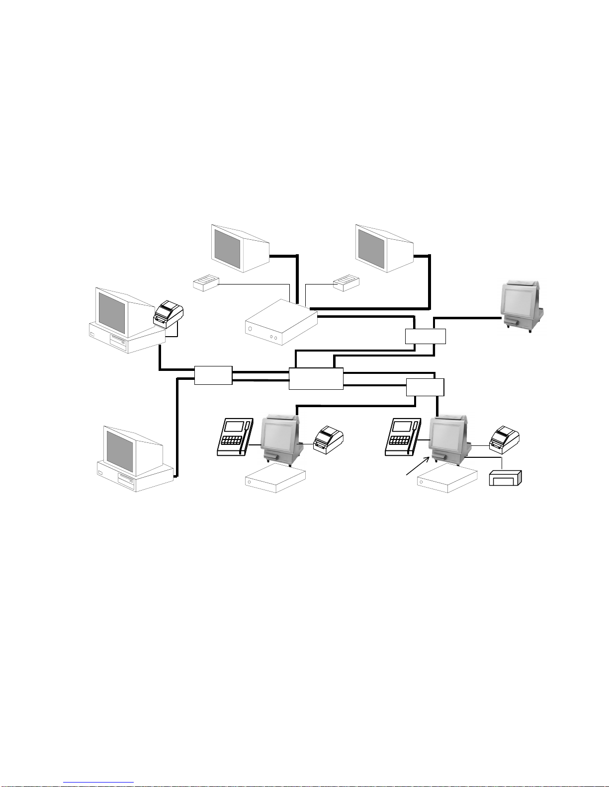
System Configurations (Example)
VGA Monitor
150MS
Printer (TM-88)
150DC
CCU
J B
J B
Card Reader 170FR
ISPISP
CCU: Communication Control Unit
ISP: In-Store Processor
170FR: Front counter Register
150DC: Dri ve Through Cont rol l er
170CD: Cash Drawer
150MS: Bump Bar
160RD: Remote Display
170MG:Card Reader
170CD
HUB
J B
170MG
160RD
1-1
Specifications
Processor, Chipset and BIOS
♦
CPU Intel Mobile Pentium I I 266MHz or 333 MHz (BGA1) CORE + 1.6V
Chipset Intel 440BX/PIIX4E
BIOS Phoenix BIOS
Memory
♦
•
Main memory
Capacity 64MB Standard
Slot 168pin DIMM Slot x 2
Type 3.3V SDRAM supported
Note
z
One 64MB SDRAM is mounted on socket -1 as factory standard.
z
Each slot can have 16 MB (minimum) to 128 MB (maximum) memory module.
z
Maximum height of DIMM is 35.65mm.
z
EDO isn't being supported.
•
L2 Cache (Secondary Cache)
256KB on CPU die
256MB Maximum
One slot occupied by standard memory
•
Video memory
4MB in VGA Controller (Not expandable)
•
BIOS ROM
Capacity 512KB
Type Flash memory (Fujits u MBM29F040 or compatible)
♦
Drives
Floppy disk drive Opti on, external One 3.5 type drive unit (1.44MB/720KB)
Hard disk drive
♦
Clock
Tolerance Monthly ± 3 minutes (Temperature 25°C)
♦
Back-up Method
•
Real Time Clock (RTC)
Battery Lithium battery, 560mAh
Battery life 8 years (need to be changed every 8 years)
Retention time 8 years (On condition that unit is turned on for 12 hours per a day)
•
Power supply
Battery Ni-Cd battery, 1200mAh
Battery life 2 years(need to be changed every 2 years)
Retention time 2 minutes
Standard, internal One 2.5 type EIDE drive unit (4.0GB or more)
Option, internal One 2.5 type EIDE drive unit
- On condition that the battery i s fully charged at installat i on
(Registers must be powered on for more than 72 hours for full battery charge)
- No display on the LCD during AC off
1-2

♦
Display
•
Crew display
Display unit TFT type LCD with Dual Back Light
Resolution 800 x 600 (SVGA)
Dot pitch 0.3 mm
Display size 12.1 type
Contrast adjust Not needed
•
Customer display
Display unit Fluorescent display tube
Color Green
Number of digits 20 characters (5 x 7dots, 9 x 6 mm) x 2 lines
Interface Serial shared with COM3 (TTL level)
♦
Touch Panel
Type Resistive
Life Resistive over 10 million times by f inger touch
Interface Serial interface (using internal COM4, TTL level)
Size 12.1 type
(It is possible to switch between Customer Display and External COM3 port by
software)
(Simulates human finger, Shape of rubber end:R8, Hardness:60°, Load:200g,
Frequency:5 Hz)
♦
Local Area Network
Interface Ethernet (10BASE-T/100BASE-TX)
Speed 10M /100Mbps
Connector 8-pin Modular Jack (RJ-45)
Wake on LAN Supported
♦
Magnetic Card Reader (Option:U24/U25 t ype )
Track ISO1/ISO2
Swipe speed 10 - 120 (maximum) cm /s
Maximum swipe speed will be reduced when dual track reader is used.
Interface Data is received as keyboard dat a
Limitation On MS-DOS, magnetic card reader doesn't work with US B keyboard.
Life Over 1 million swipe
♦
Buzzer
Buzzer volume is fixed.
♦
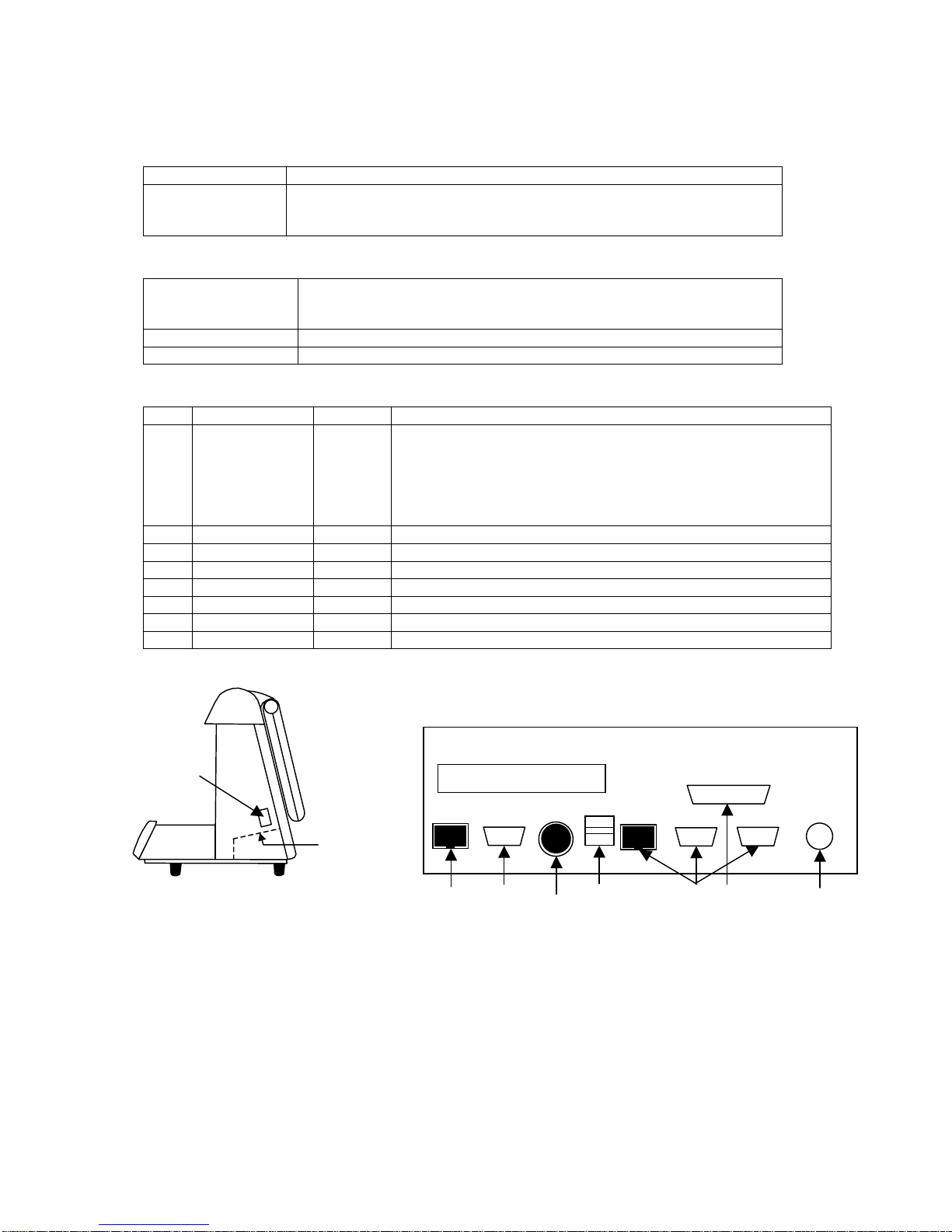
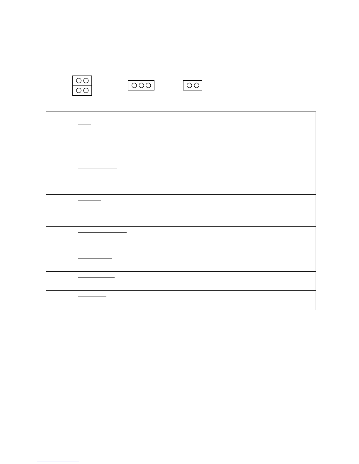
LED
Four status indicators on front panel.
LAN
CARD
3
2
1
4
1 Power (Green : Running, Red : Stand-by)
2 Hard disk (Light on access )
3 LAN (Light on LAN activity)
4 Card Reader (Green : Good, Red : Error)
1-3
♦
Expansion Slot (Option)
Either one of the below can be added on main board as an expansion slot.
PCMCIA Slot 1 Type III or 2 Type II (Support PCMCIA/CardBus)
PCI Slot 1 PCI Bus Slot
♦
Supply Voltage
Voltage 100V system : AC 90V~132V
Power consumption Approx. 60W
Frequency 50/60 Hz
♦
Connectors
No Interface Number Connector type
1 Serial 3 COM1/2 : 9pin D-s ub connector, male
2 Cash Drawer 1 6pin DI N connector, female
3 Parallel 1 25pin D-SUB connector, female
4 Video 1 15pin D-SUB c onnector, female (VGA)
5 LAN 1 8-pin Modular Jack (RJ-45)
6 USB 2 USB Connect or
7 Keyboard 1 6pin mini DIN connector
8 Floppy Disk 1 26pin mini I/O connector
Maximum PCI card size (mm) :
174.63×106.68×(component side 14.48 + rear side 2.67)
200V system : AC 198V~264V
Depending on destination, Factory setting, Not changeable
COM3 : 8pin modular connector
NOTE : COM3 is shared with Customer Display interface.
(It is possible to switch between Custom er Display and External COM3 port
by software)
Floppy Disk
8
Connectors
See Appendix for pin assignments of each connector.
5
1-4
3
2
4
6
1
7

♦
Operation Condition
Temperature 5°C - 40°C (41°F - 104°F)
Humidity 20% RH - 85% RH (no dew)
♦
Dimension and Weight
Width 250 mm (9.8 inches) (Crew display : 312mm)
Depth 320 mm (12.6 inches)
Height 365 mm (14.4 inches) with rubber foot
Weight Approx. 10 kg
Tilt angle
35°
15°
♦
Material
Case body Stainless steel s heet
Top cover ABS
♦
Supported OS
Microsoft MS-DOS, Windows 95, Windows NT Workstation 4.0
♦
Accessory
AC cable 1pc (2.5m)
♦
Safety Standard
Safety Standard............. TÜV
EMI................................FCC Part15 Class A
UL
CISPR Class B
CE
C-tick
1-5
Memory Map
FFFFFFFF
FFFE0000
FFFC0000
04000000
03C00000
10000000
01000000
(16M)
00100000
000E0000
000D0000
000CC000
000C0000
BIOS ROM
Reserve
Don’t use
Reserve
External RAM (DIMM)
(256M)
Option RAM
Main RAM (DIMM)
BIOS ROM (128K)
Reserve
VGA-BIOS
Video RAM (128K)
Same with the area of 000E0000 to 000FFFFF
7FFFF
60000
60000
40000
20000 20000
00000
SystemBIOS
+
VGA-BIOS
POSDIAG
000A0000
Main RAM (640K)
00000000
Note: BIOS ROM always selects Bank0 after resetting t he hardware.
1-6
I/O Port Map
Address (HEX) Devices used for JS-170FR
0000 - 001F DMA Controller (1) (82371EB)
0020 - 0021 Interrupt Controller (Master) (82371EB)
0022 - 0023 443BX Chip Set (82443BX)
0024 - 0027 Reserve
0040 - 005F Timer Controller (82371EB)
0060 - 006F Keyboard Controller (IT8763F)
0070 - 007F RTC, NMI Mask
0080 7-Segment for POST
0080 - 009F DMA Page Register (82371EB)
00A0 - 00BF Interrupt Controller (Slave) (82371EB)
00C0 - 00DF DMA Controller (2) (82371EB)
00F0•00FF Co-Processor
*190 7-segment LED for Test
01F0 - 1F8 Hard Disk (82371EB)
0279 IT8661F
02E0 - 02EF Reserve
02E8 - 02EF (COM4) Reserve
02F8 - 2FF Serial Port COM (2) (IT8763F)
0300 - 031F ETHERNET (RTL8139B)
0320 - 032F JS-170FR System Extension Port
0378 - 037F Parallel Port (1) (IT8763F)
03B0 - 03DF SVGA Cont rol l e r (SM710)
03E8 - 03EF (COM3) Reserve
03F0 - 03F7 Diskette Controller (IT8763F)
03F8 - 3FF Serial Port COM (1) (IT8763F)
0A79 IT8661F
0CF8 - 0CFF 430TX Chip Set (82443BX)
3220 - 3227 Serial P ort COM (3) (PC16552DV)
3228 - 322F Serial Port COM (4) (PC16552DV)
Note: ETHERNET I/O Port Map Not Fixed.
1-7
Interrupt Level
Interrupt Level Description
SMI (Power Management)
NMI I/O Check, Parity Error, Power Management
IRQ 0 Timer Output
IRQ 1 Keyboard Output Buffer Full (IT8763F)
IRQ 2 8259 Slave Side Interrupt
IRQ 3 Serial Port COM (2) (IT8763F)
IRQ 4 Serial Port COM (1) (IT8763F)
IRQ 5 Reserve
IRQ 6 Diskette Controller (IT8763F)
IRQ 7 Parallel Port1 (IT8763F)
IRQ 8 Real Time Clock (82371EB)
IRQ10 Serial Port COM (4) (PC16552DV )
IRQ11 Serial Port COM (3) (PC16552DV)
IRQ12 Mouse (IT8763F)
IRQ13 Co-processor (CPU)
IRQ14 Hard Disk (Primary) (IDE)
IRQ15 Hard Disk (Secondary) (IDE)
Note : the jumper of the hardware should change The Interrupt of Power Management.
: ETHERNET Interrupt Level Not Fixed.
1-8

Pin assignments
Serial
COM1
COM2
9 pin D-SUB Male
No IN/OUT Signal
1INCD
2INRD
3OUTTD
4 OUT DTR
5GND
6INDSR
7OUTRTS
8INCTS
9INRI
9 pin D-SUB Male
No IN/OUT Signal
1INCD
2INRD
3OUTTD
4 OUT DTR
5GND
6INDSR
7OUTRTS
8INCTS
9INRI
COM3
8 pin Modular
No IN/OUT Signal
1FG
2OUTRTS
3INRD
4 IN DS R or +5V or CD (Default)
5OUTTD
6 OUT DTR
7GND
8 IN CTS (Def aul t) or Not Connected
1-9

Cash Drawer
Parallel
6 pin DIN Female
No IN/OUT Signal
1 OUT Drawer_Open
2GND
3 IN Drawer_Status
4GND
5 IN Drawer Type
6GND
25 pin D-SUB Female
No IN/OUT Signal
1 IN/OUT STROBE*
2 IN/OUT Data Bit 0
3 IN/OUT Data Bit 1
4 IN/OUT Data Bit 2
5 IN/OUT Data Bit 3
6 IN/OUT Data Bit 4
7 IN/OUT Data Bit 5
8 IN/OUT Data Bit 6
9 IN/OUT Data Bit 7
10 IN ACK*
11 IN BUSY
12 IN PE
13 IN SLCT
14 OUT AUTO FD XT*
15 IN ERROR*
16 OUT INIT*
17 OUT SLCT IN*
18 GND
19 GND
20 GND
21 GND
22 GND
23 GND
24 GND
25 GND
1-10
Video
LAN
15 pin D-SUB Female
No IN/OUT Signal
1 OUT Video_Red
2 OUT Video_Green
3 OUT Video_Blue
4NC
5GND
6 Video GND(Red)
7 Video GND(Green)
8 Video GND(Blue)
9NC
10 GND
11 NC
12 IN/OUT SDA
13 OUT H-Sync
14 OUT V-Sync
15 IN/OUT SCL
8 pin Modular (RJ-45)
USB
No IN/OUT Signal
1OUTTX+
2OUTTX-
3INRX+
4NC
5NC
6INRX-
7NC
8NC
USB Connector
No IN/OUT Signal
1, 5 +5V
2, 6 IN/OUT USB_Data3, 7 IN/OUT USB_Data+
4, 8 GND
1-11

Keyboard
Floppy Disk
6 pin mini DIN
No IN/OUT Signal
1 IN/OUT Keyboard_Data
2 IN/OUT Mouse_Data
3GND
4+5V
5 IN/OUT Mouse_Clock
6 IN/OUT Keyboard_Clock
26 pin mini I/O Connector
No IN/OUT Signal
1GND
2 IN INDEX*
3+5V
4DRV0
5GND
6 IN DCHG0*
7NC
8NC
9NC
10 +5V
11 OUT MTR0*
12 OUT DIR
13 DENSEL
14 OUT STEP*
15 GND
16 OUT WDATA*
17 GND
18 OUT WGATE*
19 GND
20 IN TRK0*
21 GND
22 IN WRPRT*
23 IN RDATA*
24 GND
25 OUT SIDESEL0
26 NC
1-12
PCI Interface
32bit Edge Connector, 5V system
No B side A side
1 -12V TRST#
2 TCK +12V
3GND TMS
4TDO TDI
5+5V +5V
6+5V INTA#
7INTB# INTC#
8 INTD# +5V
9 PRSNT1# Reserved
10 Reserved +5V(I/O)
11 PRSNT2# Reserved/SERIRQ
12 GND GND
13 GND GND
14 Reserved Reserved
15 GND RST#
16 CLK +5V(I/O)
17 GND GNT#
18 REQ# GND
19 +5V(I/O) R eserved/PME#
20 AD[31] AD[30]
21 AD[29] +3.3V
22 GND AD[28]
23 AD[27] AD[26]
24 AD[25] GND
25 +3.3V AD[24]
26 C/BE[3]# IDSEL
27 AD[23] +3.3V
28 GND AD[22]
29 AD[21] AD[20]
30 AD[19] GND
31 +3.3V AD[18]
32 AD[17] AD[16]
33 C/BE[2]# +3.3V
34 GND FRAME#
35 IRDY# GND
36 +3.3V TRDY#
37 DEVSEL# GND
38 GND STOP#
39 LOCK# +3.3V
40 PERR# SDONE
41 +3.3V SBO#
1-13
IDE Interface
No B side A side
42 SERR# GND
43 +3.3V PAR
44 C/BE[1]# AD[15]
45 AD[14] +3.3V
46 GND AD[13]
47 AD[12] AD[11]
48 AD[10] GND
49 GND AD[09]
50 KEY KEY
51 KEY KEY
52 AD[08] C/BE[0]#
53 AD[07] +3.3V
54 +3.3V AD[06]
55 AD[05] AD[04]
56 AD[03] GND
57 GND AD[02]
58 AD[01] AD[00]
59 +5V(I/O) +5V(I/O)
60 ACK64# REQ64#
61 +5V +5V
62 +5V +5V
44pin Flat cable connector 2.0mm pitch
No IN/OUT Signal
1 IN IDERST#
2GND
3IN/OUTDATA7
4IN/OUTDATA8
5IN/OUTDATA6
6IN/OUTDATA9
7IN/OUTDATA5
8IN/OUTDATA10
9IN/OUTDATA4
10 IN/OUT DATA11
11 IN/OUT DATA3
12 IN/OUT DATA12
13 IN/OUT DATA2
14 IN/OUT DATA13
15 IN/OUT DATA1
16 IN/OUT DATA14
17 IN/OUT DATA0
18 IN/OUT DATA15
19 GND
20 -
1-14

No IN/OUT Signal
21 OUT DMARQ
22 GND
23 IN IOW#
24 GND
25 IN IOR#
26 GND
27 OUT *IORDY
28 IN CSEL
29 IN DMACK#
30 GND
31 OUT INTRQ
32 33 IN DA1
34 IN -(MASTER/SLAVE)
35 IN DA0
36 IN DA2
37 IN CS1#
38 IN CS3#
39 OUT DASP#
40 GND
41 +5V
42 +5V
43 GND
44 -
1-15

Dip Switches and Jumpers
Dip Switch 1
61
Bit Explanation
1 Model identification bit
On : 0 for I/O 324H bit5
Off : 1 for I/O 324H bit5 (Factory setting)
Extended I/O port 324H bit 5 reflects to this setting.
2 Touch panel type
On : Douwa (Carrol Touch) type (Factory setting f or Germany Model only)
Off : Fujitsu type (Factory Setting)
Touch panel has two kinds of operating m ode. Set this bit to Off (Fuj itsu type) when you use Windows touch panel
driver. For use with McDonald's application, set this bi t to On (Douwa or Carrol Touch type).
3 Circuit for decoding (Magnetic card Swipe Reader : MSR)
On : Circuit 2 (Formerly cal l ed as MAG2) (Factory setting)
Off : Circuit 1 (Formerly c al l ed as MAG1)
This model has two circuits (circuit 1 and 2) to decode dat a on magnetic stripe of card. Combi nation of a c i rcuit and a
track (a data stream on t he magnetic stripe) is determined by dip switch 1 bit 5/6. (See below)
When "Single" i s set by dip switch 1 bit 4, only a c i rcuit set by this bit is used for data decoding. When "Dual" is set by
dip switch bit 4, both circ ui t 1 and 2 can be used to decode data. Bit 3 has no effect in this case.
4 Single and Dual circuit (Magnetic card Swipe Reader : MSR)
On : Single (Factory setting)
Off : Dual
When this bit is set to "Single", the circuit selected by bit 3 is used to decode data and appli cation receives dat a of a
track defined by bit 5/6 through the circuit.
"Dual" setting uses both circuit 1 and 2 to decode data and application receives data of two tracks if both are on the
card. Only data of existing track is returned to application even if this bit is set to "Dual".
6-5 Circuit and Track (Magnetic card Swipe Reader : MSR)
bit6/5 is Off/Off : Circuit 1 expects JIS-II (J apan), circuit 2 expects ISO2 (J IS-I track2, Japan).
bit6/5 is Off/On : Circ ui t 1 expects ISO1 (JIS-I trac k1, Japan), circuit 2 expects JIS-II.
bit6/5 is On/Off : Circuit 1 expects ISO2, circuit 2 expects ISO1.
bit6/5 is On/On : Circuit 1 expects ISO1, circuit 2 expects ISO2.
Combination of these bits tells circ uit to decode specified track data. For example c ircuit 1 decodes only ISO1 and
circuit 2 decodes only IS O2 i f bi t 6/5 is On/On. If IS O2 dat a i s input to circuit 1, it is treated as an error.
1-16
Dip Switch 2
81
Bit Explanation
1 Address control for extended I/O
On : Software can enable/disable access to extended I/O ports. (Factory setting)
Off : Extended I/O is always enabled.
When this bit is s et to On, software can enable/ disable access to extended I/O ports (320H-32DH) by output data to
32FH.
Setting this bit to Off always enables ac cess to extended I/O. Software can't disable ac cess to extended I/O through
32FH.
System initiali zes hardware to disabling extended I/O if thi s bit is s et to On. But BI OS setup f inally determi nes initial
state of accessibilit y, enable or disable.
2 Reserved for future
Off : (Factory setting)
Extended I/O 32DH bit5 reflects to t his s ett ing. This bit i s res erved for f uture enhanc em ents and any func ti ons are not
currently assigned to this bit.
4-3 Signal to open drawer
bit4/3 is Off/Off : 217ms
bit4/3 is Off/On : 145ms (Factory setting)
bit4/3 is On/Off : 108ms
bit4/3 is On/On : 72ms
These bits define the period to activate signal for drawer open. Do not change thes e bi ts unless electrical specification
of the drawer is modified in fut ure.
5 Type of customer display
On : Dual line type
Off : One line type
This bit is used to get t ype of cust omer dis play, one line type or dual. This bit actuall y reflects the st atus of di p switc h
2 bit5. Setting this switch to OFF returns 1 to this bit.
Extended port 32DH bit0 reflects to t his bit. This bit should be set to indicate the customer display type actually
connected if application program has a capability to adjust data for each display type.
6 Reserved for future
Off : (Factory setting)
Extended I/O 32DH bit1 reflects to t his s ett ing. This bit i s res erved for f uture enhanc em ents and any func ti ons are not
currently assigned to this bit.
8-7 Type of LCD
bit7/6 is
11 : VGA (640x480)
10 : SVGA (800x600)
01 : XGA (1024x768)
00 : Reserved.
Bit8/7 is Off/Off : VGA (640x480) (Factory setting)
Bit8/7 is Off/On : SV G A (800x600)
Bit8/7 is On/Off : XGA (1024x768)
Bit8/7 is On/On : Reserved.
Extended port 32DH bit6/7 reflects to these bits.
1-17
Jumper pins
Jumper numbers and pin numbers are printed on the main board. Direction of the jumpers follow the direction of printed
numbers.
1
23
Pin Explanation
JP1 VGAC
JP2 Power fail interrupt
JP3 COM3 IRQ
JP4/5/6 Control signal of COM3
JP7 CPU I/O voltage
JP8 CPU GTL voltage
JP9 Power control
4
3
12
1-4 Short, 2-3 Short : 640x480 (Factory sett i ng)
1-4 Short, 2-3 Open : 1024x768
1-4 Open, 2-3 Short : 800x600
1-4 Open, 2-3 Open : 1280x1024
This jumper sets t he type of connected LCD to VGA cont rol l er.
1-2 Short : NMI (Factory setting)
2-3 Short : SMI
This jumper defines the type of interrupt by power fail.
1-2 Short : IRQ11 (Factory setting)
2-3 Short : IRQ4
This jumper sets I RQ (i nterrupt) number used by COM3 UART.
This jumper defines functions of some cont rol l i nes on 8-pin modular connector of COM3.
See table below for combination of pi ns.
1-2 Short : +2.5V (Factory setting)
2-3 Short : Reserved.
Short : GTL=CORE voltage (Factory se t ting)
Open : Reserved.
Short : Boot by main power switc h
Open : Boot by front power switch (Factory s et ting)
1
2
1-18
Signal on COM3 connector
JP4 Explanation
1-2 Short Pin8 is CTS (Factory setti ng)
2-3 Short Pin8 is Ground. CTS is always act i ve.
JP5 JP6 Explanation
1-2 Short 2-3 Short Pin4 is DCD. DSR is always active. (Factory setting)
2-3 Short 2-3 Short Pin4 is DSR. DCD is always inactive.
1-2 Short 1-2 Short Pin4 is fixed to +5V. DSR is always acti ve and DCD i s inactive.
2-3 Short 1-2 Short Pin4 is f i xed to +5V. DSR and DCD are always inactive.
1-19

1-20
 Loading...