

© Panasonic Corporation 2013 Unauthorized copying and distribution is a violation of law.
ORDER NO. VM1301002CE
B27
High Definition Video Camera
Model No. HC-V520P
HC-V520PC
HC-V520EB
HC-V520EF
HC-V520EG
HC-V520EP
HC-V520EE
HC-V520GC
HC-V520GK
HC-V520MPU
HC-V520MGK
HC-V520MGN
HC-V520MGT
HC-V510PC
HC-V510PU
HC-V510EG
HC-V510EF
HC-V510EP
HC-V510EB
HC-V510EE
HC-V510GC

2
Colour
(K)...........Black Type (except HC-V520GC/GK/
V520MGK/V510GC)
(S)...........Silver Type (only HC-V520EG/V510EG/EE)
(W)...........White Type (only HC-V520GC/GK/V520MGK/
V510GC)
(P)...........Pink Type (only HC-V520GC/GK/V520MGK/
V510GC)
(R)...........Red Type (only HC-V520EG/EP/EB/V510EG/
EB/EE)
(A)...........Blue Type (only HC-V520GC/V510GC)
TABLE OF CONTENTS
PAG E PAG E
1 Safety Precautions -----------------------------------------------3
1.1. General Guidelines ----------------------------------------3
1.2. Leakage Current Cold Check ---------------------------3
1.3. Leakage Current Hot Check (See Figure. 1) --------3
2Warning--------------------------------------------------------------4
2.1. Prevention of Electrostatic Discharge (ESD)
to Electrostatically Sensitive (ES) Devices ----------4
2.2. How to Recycle the Lithium Ion Battery (U.S.
Only)-----------------------------------------------------------4
2.3. Caution for AC Cord (For EB/GC) ---------------------5
2.4. How to Replace the Lithium Battery -------------------6
3 Service Navigation------------------------------------------------7
3.1. Introduction --------------------------------------------------7
3.2. General Description About Lead Free Solder
(PbF) ----------------------------------------------------------7
3.3. Important Notice 1:(Other than U.S.A. and
Canadian Market) ------------------------------------------7
3.4. How to Define the Model Suffix (NTSC or PAL
model)---------------------------------------------------------8
3.5. Formatting----------------------------------------------------9
3.6. Baking of replacement IC and defective P.C.B.
----------------------------------------------------------------10
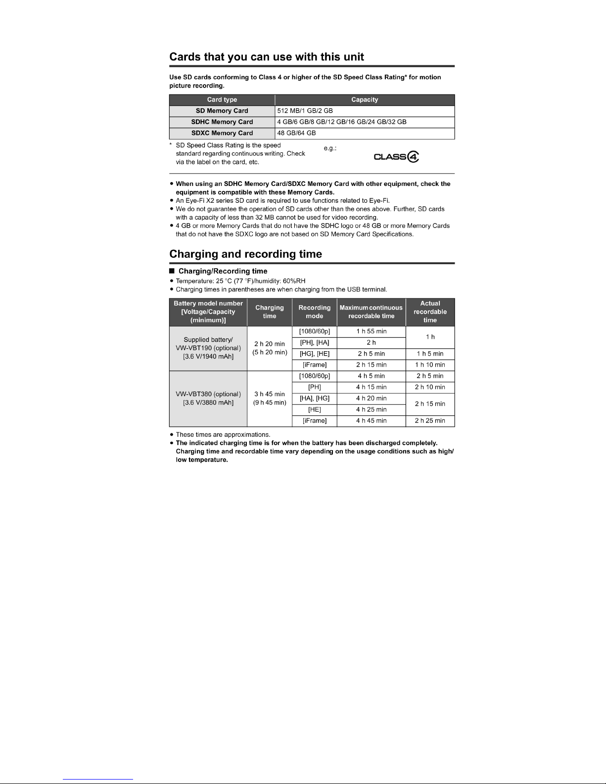
4 Specifications ---------------------------------------------------- 11
4.1. For NTSC Areas------------------------------------------ 11
4.2. For PAL Areas -------------------------------------------- 16
5 Location of Controls and Components------------------ 21
6 Service Mode ----------------------------------------------------- 25
6.1. Built-in Memory Self Check Execution (HCV520M only) ----------------------------------------------- 26
6.2. Lock Search History Indication ----------------------- 26
6.3. Power ON Self Check Result Display---------------27
6.4. Erasing the lock histories ------------------------------ 27
6.5. Camera data indications while the video
playback ---------------------------------------------------- 28
6.6. Adjustment function for the Service ----------------- 29
6.7. Restore the backed up adjustment data------------ 30
6.8. Touch Panel Calibration -------------------------------- 31
6.9. NFC Initialization (HC-V520/V520 only) ------------ 31
7 Service Fixture & Tools --------------------------------------- 32
7.1. When Replacing the Main P.C.B. -------------------- 32
7.2. Service Position ------------------------------------------ 32
8 Disassembly and Assembly Instructions--------------- 33
8.1. Disassembly Flow Chart for the Unit ---------------- 33
8.2. PCB Location---------------------------------------------- 33
8.3. Disassembly Procedure for the Unit ---------------- 34
9 Measurements and Adjustments -------------------------- 47
9.1. Electric Adjustment-------------------------------------- 47
10 Factory Setting -------------------------------------------------- 60
10.1. How To Turn On The Factory Settings? ----------- 60
10.2. What Is The Factory Settings? ----------------------- 61
11 Block Diagram--------------------------------------------------- 62
11.1. Overall Block Diagram---------------------------------- 62
11.2. Camera/System Control Circuit Block
Diagram ---------------------------------------------------- 63
11.3. Video/Audio Signal Process(1) Circuit Block
Diagram ---------------------------------------------------- 64
11.4. Video/Audio Signal Process(2) Circuit Block
Diagram ---------------------------------------------------- 65
11.5. Lens Drive Circuit Block Diagram ------------------- 66
11.6. Power Supply Circuit Block Diagram --------------- 67
12 Wiring Connection Diagram -------------------------------- 68
12.1. Interconnection Diagram------------------------------- 68
3
1 Safety Precautions
1.1. General Guidelines
1. IMPORTANT SAFETY NOTICE
There are special components used in this equipment
which are important for safety. These parts are marked by
in the Schematic Diagrams, Circuit Board Layout,
Exploded Views and Replacement Parts List. It is essential that these critical parts should be replaced with manufacturer’s specified parts to prevent X-RADIATION,
shock, fire, or other hazards. Do not modify the original
design without permission of manufacturer.
2. An Isolation Transformer should always be used during
the servicing of AC Adaptor whose chassis is not isolated
from the AC power line. Use a transformer of adequate
power rating as this protects the technician from accidents resulting in personal injury from electrical shocks. It
will also protect AC Adaptor from being damaged by accidental shorting that may occur during servicing.
3. When servicing, observe the original lead dress. If a short
circuit is found, replace all parts which have been overheated or damaged by the short circuit.
4. After servicing, see to it that all the protective devices
such as insulation barriers, insulation papers shields are
properly installed.
5. After servicing, make the following leakage current
checks to prevent the customer from being exposed to
shock hazards.
1.2. Leakage Current Cold Check
1. Unplug the AC cord and connect a jumper between the
two prongs on the plug.
2. Measure the resistance value, with an ohmmeter,
between the jumpered AC plug and each exposed metallic cabinet part on the equipment such as screwheads,
connectors, control shafts, etc. When the exposed metallic part has a return path to the chassis, the reading
should be between 1 MΩ and 5.2 MΩ. When the exposed
metal does not have a return path to the chassis, the
reading must be infinity.
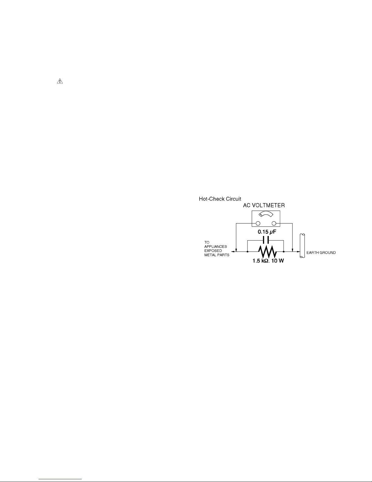
1.3. Leakage Current Hot Check
(See Figure. 1)
1. Plug the AC cord directly into the AC outlet. Do not use
an isolation transformer for this check.
2. Connect a 1.5 kΩ, 10 W resistor, in parallel with a 0.15 μF
capacitor, between each exposed metallic part on the set
and a good earth ground, as shown in Figure. 1.
3. Use an AC voltmeter, with 1 kΩ/V or more sensitivity, to
measure the potential across the resistor.
4. Check each exposed metallic part, and measure the voltage at each point.
5. Reverse the AC plug in the AC outlet and repeat each of
the above measurements.
6. The potential at any point should not exceed 0.75 V RMS.
A leakage current tester (Simpson Model 229 or equivalent) may be used to make the hot checks, leakage current must not exceed 1/2 mA. In case a measurement is
outside of the limits specified, there is a possibility of a
shock hazard, and the equipment should be repaired and
rechecked before it is returned to the customer.
Figure. 1
4
2Warning
2.1. Prevention of Electrostatic Discharge (ESD) to Electrostatically
Sensitive (ES) Devices
Some semiconductor (solid state) devices can be damaged easily by static electricity. Such components commonly are called Electrostatically Sensitive (ES) Devices. Examples of typical ES devices are integrated circuits and some field-effect transistors and
semiconductor "chip" components. The following techniques should be used to help reduce the incidence of component damage
caused by electrostatic discharge (ESD).
1. Immediately before handling any semiconductor component or semiconductor-equipped assembly, drain off any ESD on your
body by touching a known earth ground. Alternatively, obtain and wear a commercially available discharging ESD wrist strap,
which should be removed for potential shock reasons prior to applying power to the unit under test.
2. After removing an electrical assembly equipped with ES devices, place the assembly on a conductive surface such as aluminum foil, to prevent electrostatic charge buildup or exposure of the assembly.
3. Use only a grounded-tip soldering iron to solder or unsolder ES devices.
4. Use only an antistatic solder removal device. Some solder removal devices not classified as “antistatic (ESD protected)” can
generate electrical charge sufficient to damage ES devices.
5. Do not use freon-propelled chemicals. These can generate electrical charges sufficient to damage ES devices.
6. Do not remove a replacement ES device from its protective package until immediately before you are ready to install it. (Most
replacement ES devices are packaged with leads electrically shorted together by conductive foam, aluminum foil or comparable conductive material).
7. Immediately before removing the protective material from the leads of a replacement ES device, touch the protective material
to the chassis or circuit assembly into which the device will be installed.
CAUTION :
Be sure no power is applied to the chassis or circuit, and observe all other safety precautions.
8. Minimize bodily motions when handling unpackaged replacement ES devices. (Otherwise harmless motion such as the
brushing together of your clothes fabric or the lifting of your foot from a carpeted floor can generate static electricity (ESD) sufficient to damage an ES device).
2.2. How to Recycle the Lithium Ion Battery (U.S. Only)
5
2.3. Caution for AC Cord
(For EB/GC)
2.3.1. Information for Your Safety
IMPORTANT
Your attention is drawn to the fact that recording of prerecorded tapes or discs or other published or broadcast
material may infringe copyright laws.
WARNING
To reduce the risk of fire or shock hazard, do not expose
this equipment to rain or moisture.
CAUTION
To reduce the risk of fire or shock hazard and annoying
interference, use the recommended accessories only.
FOR YOUR SAFETY
DO NOT REMOVE THE OUTER COVER
To prevent electric shock, do not remove the cover. No user
serviceable parts inside. Refer servicing to qualified service
personnel.
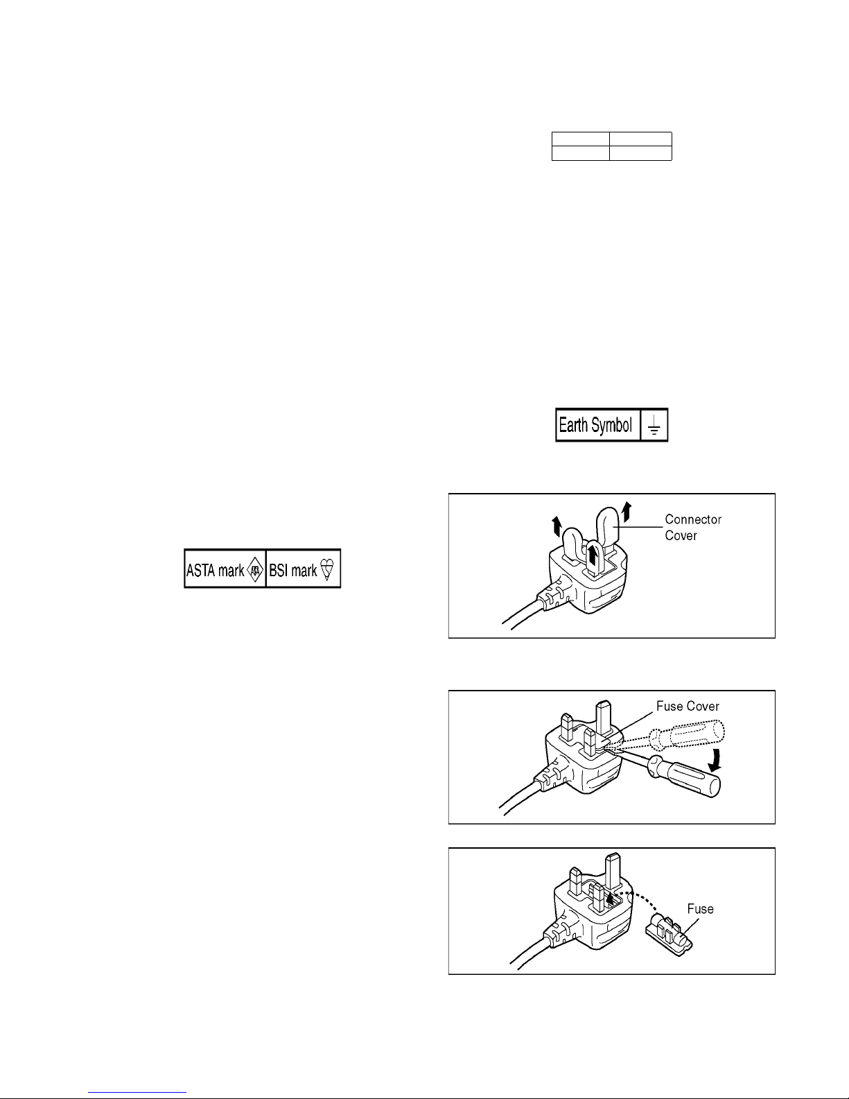
2.3.2. Caution for AC Mains Lead
For your safety, please read the following text carefully.
This appliance is supplied with a moulded three-pin mains plug
for your safety and convenience.
A 5-ampere fuse is fitted in this plug.
Should the fuse need to be replaced please ensure that the
replacement fuse has a rating of 5 amperes and it is approved
by ASTA or BSI to BS1362
Check for the ASTA mark or the BSI mark on the body of the
fuse.
If the plug contains a removable fuse cover you must ensure
that it is refitted when the fuse is replaced.
If you lose the fuse cover, the plug must not be used until a
replacement cover is obtained.
A replacement fuse cover can be purchased from your local
Panasonic Dealer.
If the fitted moulded plug is unsuitable for the socket outlet in
your home then the fuse should be removed and the plug cut
off and disposed of safety.
There is a danger of severe electrical shock if the cut off plug is
inserted into any 13-ampere socket.
If a new plug is to be fitted please observe the wiring code as
shown below.
If in any doubt, please consult a qualified electrician.
2.3.2.1. Important
The wires in this mains lead are coloured in accordance with
the following code:
As the colours of the wires in the mains lead of this appliance
may not correspond with the coloured markings identifying the
terminals in your plug, proceed as follows:
The wire which is coloured BLUE must be connected to the terminal in the plug which is marked with the letter N or coloured
BLACK.
The wire which is coloured BROWN must be connected to the
terminal in the plug which is marked with the letter L or coloured
RED.
Under no circumstances should either of these wires be connected to the earth terminal of the three pin plug, marked with
the letter E or the Earth Symbol.
2.3.2.2. Before Use
Remove the Connector Cover as follows.
2.3.2.3. How to Replace the Fuse
1. Remove the Fuse Cover with a screwdriver.
2. Replace the fuse and attach the Fuse cover.
Blue Neutral
Brown Live
6
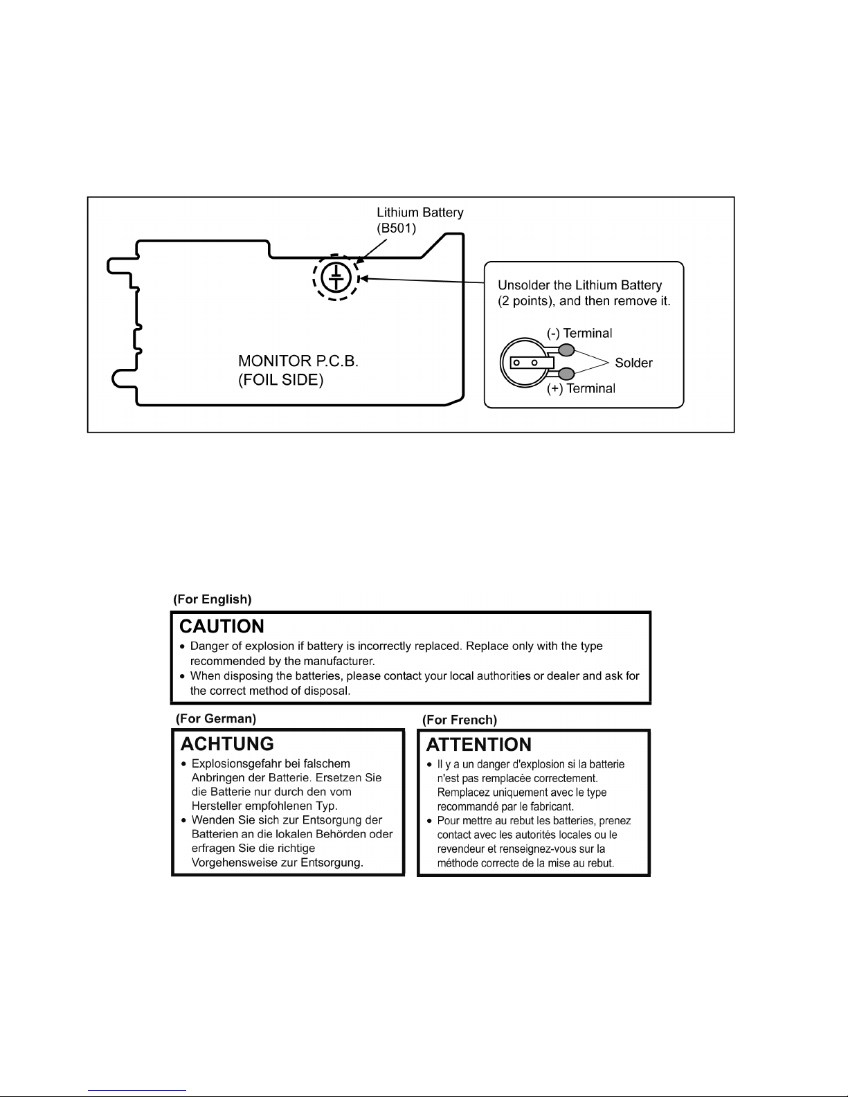
2.4. How to Replace the Lithium Battery
2.4.1. Replacement Procedure
1. Remove the MONITOR P.C.B.. (Refer to Disassembly Procedures.)
2. Unsolder the each soldering point of electric lead terminal for Lithium battery (Ref. No. “B501” at foil side of MONITOR
P.C.B.) and remove the Lithium battery together with electric lead terminal. Then replace it into new one.
NOTE:
The Type No. ML-614S/DN includes electric lead terminals.
NOTE:
This Lithium battery is a critical component.
(Type No.: ML-614S/DN Manufactured by Energy Company, Panasonic Corporation)
It must never be subjected to excessive heat or discharge.
It must therefore only be fitted in requirement designed specifically for its use.
Replacement batteries must be of same type and manufacture.
They must be fitted in the same manner and location as the original battery, with the correct polarity contacts observed.
Do not attempt to re-charge the old battery or re-use it for any other purpose.
It should be disposed of in waste products destined for burial rather than incineration.
NOTE:
Above caution is applicable for a battery pack which is for HC-V520/V520M/V510 series, as well.
1. Battery Pack for this model.
7
3 Service Navigation
3.1. Introduction
This service manual contains technical information, which allow service personnel’s to understand and service this model.
Please place orders using the parts list and not the drawing reference numbers.
If the circuit is changed or modified, the information will be followed by service manual to be controlled with original service manual.
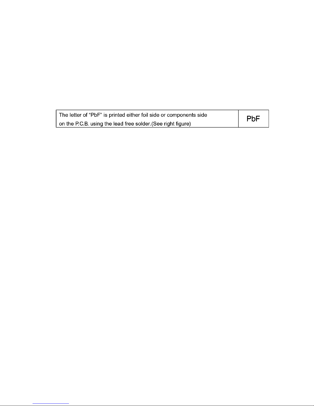
3.2. General Description About Lead Free Solder (PbF)
The lead free solder has been used in the mounting process of all electrical components on the printed circuit boards used for this
equipment in considering the globally environmental conservation.
The normal solder is the alloy of tin (Sn) and lead (Pb). On the other hand, the lead free solder is the alloy mainly consists of tin
(Sn), silver (Ag) and Copper (Cu), and the melting point of the lead free solder is higher approx.30°C (86°F) more than that of the
normal solder.
Distinction of P.C.B. Lead Free Solder being used
Service caution for repair work using Lead Free Solder (PbF)
• The lead free solder has to be used when repairing the equipment for which the lead free solder is used.
(Definition: The letter of “PbF” is printed on the P.C.B. using the lead free solder.)
• To put lead free solder, it should be well molten and mixed with the original lead free solder.
• Remove the remaining lead free solder on the P.C.B. cleanly for soldering of the new IC.
• Since the melting point of the lead free solder is higher than that of the normal lead solder, it takes the longer time to melt the
lead free solder.
• Use the soldering iron (more than 70W) equipped with the temperature control after setting the temperature at 350±30°C
(662±86°F).
Recommended Lead Free Solder (Service Parts Route.)
• The following 3 types of lead free solder are available through the service parts route.
RFKZ03D01KS-----------(0.3mm 100g Reel)
RFKZ06D01KS-----------(0.6mm 100g Reel)
RFKZ10D01KS-----------(1.0mm 100g Reel)
Note
* Ingredient: tin (Sn) 96.5%, silver (Ag) 3.0%, Copper (Cu) 0.5%, Cobalt (Co) / Germanium (Ge) 0.1 to 0.3%
3.3. Important Notice 1:(Other than U.S.A. and Canadian Market)
1. The service manual does not contain the following information, because of the impossibility of servicing at component level
without concerned equipment/facilities.
a. Schematic diagram, Block Diagram and P.C.B. layout of MAIN P.C.B..
b. Parts list for individual parts for MAIN P.C.B..
When a part replacement is required for repairing MAIN P.C.B., replace as an assembled parts. (Main P.C.B.)
2. The following category is /are recycle module part. Please send it/them to Central Repair Center.
- MAIN P.C.B. (VEP03J86C): HC-V520P/PC/EB/EF/EG/EP/EE/GC/GK
- MAIN P.C.B. (VEP03J86A): HC-V520MPU/GK/GN/GT
- MAIN P.C.B. (VEP03J86D): HC-V510PC/PU/EG/EF/EP/EB/EE/GC
8
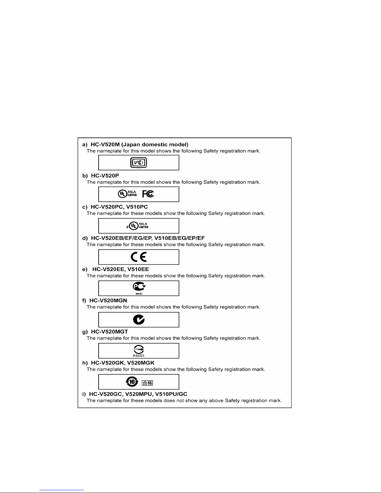
3.4. How to Define the Model Suffix (NTSC or PAL model)
There are nine kinds of HC-V520/V520M/V510.
• a) HC-V520M (Japan domestic model)
• b) HC-V520P
• c) HC-V520PC, V510PC
• d) HC-V520EB/EF/EG/EP, V510EB/EG/EP/EF
• e) HC-V520EE, V510EE
• f) HC-V520MGN
• g) HC-V520MGT
• h) HC-V520GK, V520MGK
• i) HC-V520GC, V520MPU, V510PU/GC
What is the difference is that the “INITIAL SETTING” data which is stored in Flash ROM mounted on Main P.C.B..
3.4.1. Defining methods:
To define the model suffix to be serviced, refer to the rating label and caution label which are putted on the Unit.
NOTE:
After replacing the MAIN P.C.B., be sure to achieve adjustment.
9
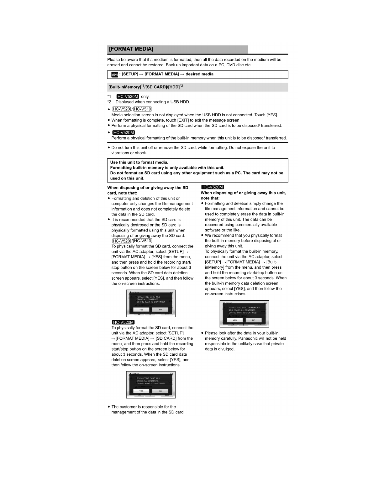
3.5. Formatting
10
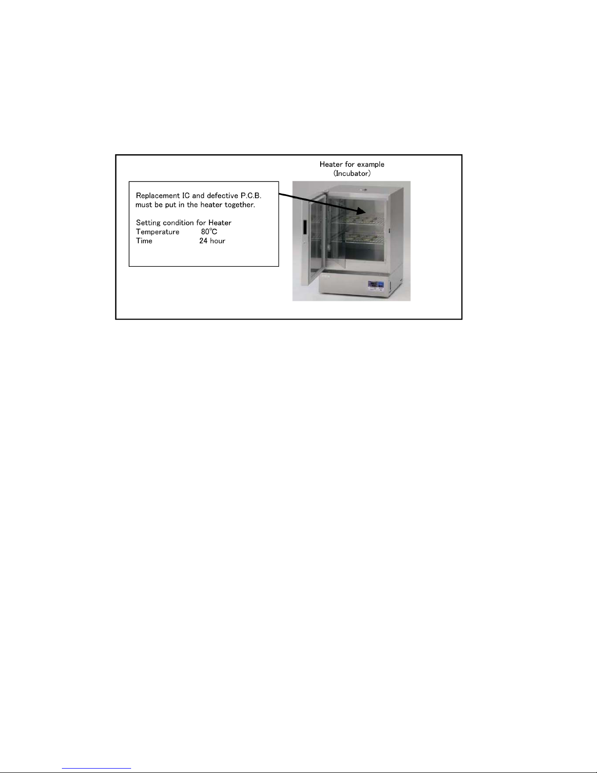
3.6. Baking of replacement IC and defective P.C.B.
When replacing the CSP/BGA/QFN type IC mounted on the P.C.B., the problem of IC crack or foil pattern breaking in the P.C.B.
might sometimes occur by rapid heating.
In order to improve the success rate of IC replacement for repair, it would be required to work out baking of replacement
IC and defective P.C.B. before replacing IC.
Please refer the way of baking as follows.
Replacement IC and defective P.C.B. must be put in the heater together.
• Baking temperature and time (Hour)
80°C / 24 hour
11
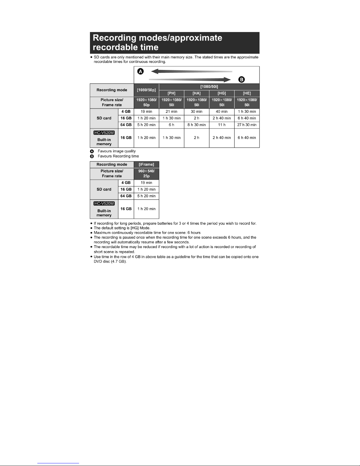
4 Specifications
4.1. For NTSC Areas

12
13
14
15
16
4.2. For PAL Areas
17
18

19
20
21
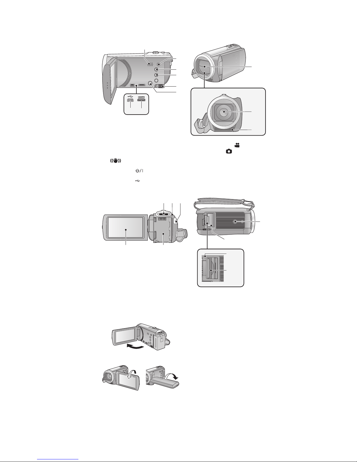
5 Location of Controls and Components
1 Speaker
2 A/V connector [A /V]
3 Intelligent auto button [iA]
4 Optical Image Stabilizer button
[ O.I.S.]
5 Battery release lever [BATT]
6 Power button [ ]
7 HDMI mini connector [HDMI]
8 USB terminal [ ]
9 Lens cover
The lens cover opens in Motion Picture
Recording Mode or Still Picture
Recording Mode.
10 Lens
11 Internal stereo microphones
1
2
3
4
5
6
78
9
10
11
●
12 Mode switch
13 Status indicator
14 Recording start/stop button
15 Battery holder
16 LCD monitor (Touch screen)
It can open up to 90Q .
Itcanrotateupto180Q towards the lens or
90Qtowards the opposite direction.
17 Tripod receptacle
If you attach a tripod which has 5.5 mm
(0.22 S) screw or larger, it may damage this
unit.
18 SD card cover
19 Access lamp [ACCESS]
20 Card slot
12 13 14
1516
17
18
19
20
●
●
●

22
21 DC input terminal [DC IN]
Do not use any other AC adaptors except the
supplied one.
22 Photoshot button [ ]
23 Zoom lever [W/T] (In Motion Picture
Recording Mode or Still Picture
Recording Mode)
Thumbnail display switch [ / ]/
Volume lever [UVOLT] (In Playback
Mode)
24 Grip belt
Adjust the length of the grip belt so that it fits
your hand.
Flip the belt.
Adjust the length.
Replace the belt.
25 Shoulder strap fixture
21
22
23
5242
●
/
26 Wi-Fi button [Wi-Fi] 27 Wi-Fi Transmitter
28 NFC touch part
HC-V520
HC-V520M
26
27
28

23
Operate the mode switch to change the mode to , or .
You can operate by directly touching the LCD monitor (touch screen) with your finger.
Touch
Touch and release the touch screen to select icon or
picture.
Touch the center of the icon.
Touching the touch screen will not operate while you
are touching another part of the touch screen.
Slide while touching
Move your finger while pressing on the touch screen.
Selecting a mode
Motion Picture Recording Mode
Still Picture Recording Mode
Playback Mode
How to use the touch screen
●
●
About the operation icons
///:
Touch when changing a page or performing settings.
:
Touchtoreturntothepreviousscreen.

24
About the Touch Menu
Touch (left side)/ (right side) of on the Touch Menu to switch the
operation icons.
It is also possible to switch the operation icons by sliding the Touch Menu right or left while
touching it.
You can change the operation icons to display.
Displayed only in Intelligent Auto Plus Mode and [Miniature Effect]/[8mm movie]/
[Silent movie] of the Creative Control Mode.
Displayed only in [Time Lapse Rec] of the Creative Control Mode , Scene Mode
and the Manual Mode.
Displayed only when connected to a TV.
Touch Menu
Recording Mode Playback Mode
T
W
MENU
T
W
FOCUS
WB
SHTR
IRIS
MENU
ALL
●
To display the Touch Menu
Do not touch on the LCD monitor with hard pointed tips, such as ball point pens.
Display of the Touch Menu will disappear when no
touch operation is performed for a specific period of
time during recording of motion picture/still picture. To
display it again, touch .
●

25
6 Service Mode
1. Indication method of the service menu
Set the mode switch “Motion Picture Recording” mode.
2. While the power is turned OFF, keep pressing the “Power” button, “Zoom lever” to W side and “intelligent auto/Manual” button
for more than 3 seconds until the top screen of the Service Mode Menu being displayed.
Service mode menu
NOTE:
Do not using service mode except above table of Service mode menu.
3. End method of the top screen of the service mode menu
Touch the [ EXIT ] of LCD to end the service mode, and then POWER OFF.
Screen display Contents Function
1 Factory settings Function to throw a product up in a factory shipment state
(When recorded data in Built-in memory, “error display” is done)
3 Built-in memory self check execution
(HC-V520M only)
Function to check self as for the state of Built-in memory
4 Lock search history indication Display the camera system error cord for three histories saved
in EEPROM
5 Power ON self check result display Power ON self check (function to diagnose correct function of
the device and interface between devices) result display
10 Erasing the lock histories Erasing the error histories (working time is not erased)
12 Camera data indications while the
video playback
Display the camera informations (Shutter speed, Iris value,
White balance and focal length) while playing recorded video
14 Adjutment function for the service The service adjustment do setup and adjustment of the follow-
ing items required in the field service.
15 Restore the backed up adjustment data Restore the adjustment data to new or repaired Main P.C.B.
from SD card that the data backed up from original Main P.C.B.
before repairs or replacement.
16 Touch panel calibration Calibrate the touch positions of the touch panel.
17 NFC initialization
(HC-V520M/V520 only)
Performs the Initialization of the NFC chip and erase the set-
tings like as Wi-Fi connection etc..

26
6.1. Built-in Memory Self Check Execution (HC-V520M only)
Touch the [ 3 ] of LCD, select Built-in memory self check execution.
Operation specifications
Indication contents
• Built-in memory self check result display
Display the Built-in memory self check execution.
Displays other than “OK” are abnormalities of Built-in memory.
Touch the [ BAK ] of LCD to end the service mode, and then POWER OFF.
6.2. Lock Search History Indication
Touch the [ 4 ] of LCD, select Lock search history indication.
Operation specifications
Indication contents
• Lock search history indication
Display the camera system error cord for three histories saved in EEPROM.
• The error cord contents which are displayed
Touch the [ BAK ] of LCD to end the service mode, and then POWER OFF.
Error code Function
51 Focus control is abnormal
52 Zoom control is abnormal
53 OIS lens control is abnormal
54 Zoom control is abnormal (2)
71 Lens cover open/close is abnormal
73 High temperature is abnormal

27
6.3. Power ON Self Check Result Display
Touch the [ 5 ] of LCD, select Power ON self check result display.
Operation specifications
Indication contents
• Power ON self check result display
Function to diagnose correct function of the device and interface between devices result display.
Display the following communication test result.
- CAM-PWR : communication test between IC3401 and IC1503
- CAM-UNI : Internal communication test of IC3401
Display other than “OK” are abnomalities of each lines.
Cutting of battery connection or AC power supply connection to end the service mode.
6.4. Erasing the lock histories
Touch the [ 10 ] of LCD, select erasing the lock histories execution.
Operation specifications
Function Description
• Erasing the error histories stored in EEPROM. (working time is not erased)
Press the power button and turn off.

28
6.5. Camera data indications while the video playback
Touch the [ 12 ] of LCD, select indicating the camera informations while playing back the recorded video.
Operation specifications
Indication contents
• While playing back the recorded videos, the camera informations (Shutter speed, Iris value, White balance and focal length) are
superimposed on the LCD screen.
Press the power button and turn off.

29
6.6. Adjustment function for the Service
Touch the [14] of LCD, select the adjustment function for the service.
Operation Specifications (until before the start of the adjustment)
Function description
The service adjustment do setup and adjustment of the following items required in the field service.
For a detailed content, such as the adjustment procedure, refer to “9 Measurements and Adjustments”.
• Setting of the file name for adjustment data backup to SD card.
• Model setting
• Execution of adjustment data backup to SD card
• Checking of Switches
• Camera adjustment (Iris, Gyro, OIS and Missing pixels)
• Zoom Tracking adjustments
• Indoor White Balance Adjustment (CH-GAIN, PWM, WB)
• Outdoor White Balance Adjustment (PWM, WB)
• Level shot adjustment
Press the power button and turn the unit off.

30
6.7. Restore the backed up adjustment data
Touch the [15] of LCD, select restoring the backed up adjustment data from SD card to the unit.
Operation Specifications
Function description
Restore the adjustment data to new or repaired Main P.C.B. from SD card that the data backed up from original Main P.C.B.
before repairs or replacement.
To backup the adjustment data, use “6.6. Adjustment function for the Service”.
Restoring procedure
Press the power button and turn the unit off.

31
6.8. Touch Panel Calibration
Touch the [16] of LCD, select the calibration of touch panel.
Operation Specifications
Function description
Calibrate the touch positions of the touch panel.
Press the power button and turn the unit off.
6.9. NFC Initialization (HC-V520/V520 only)
Touch the [17] of LCD, select initialization of NFC (Near Field Communication) function.
Operation Specifications
Function description
This function performs the Initialization of the NFC chip and erase the settings like as Wi-Fi connection etc..
Press the power button and turn the unit off.

32
7 Service Fixture & Tools
7.1. When Replacing the Main P.C.B.
After replacing the MAIN P.C.B., be sure to achieve adjustment.
7.2. Service Position
This Service Position is used for checking and replacing parts. Use the following Extension cables for servicing.
Table S1 Extension Cable List
No. Parts No. Connection Form
1 RFKZ0354 FP6001(MAIN) - MONITOR FPC 37PIN 0.3 FFC
2 RFKZ0444 PP6001(MAIN) - PS6401(SD HOLDER) 50PIN 0.5 B to B
3 VFK1480 FP6003(MAIN) - ECM FPC 6PIN 0.5 FFC
4 VFK1440 FP6402(SD HOLDER) - TOP OPERATION 10PIN 0.5 FFC

33
8 Disassembly and Assembly Instructions
8.1. Disassembly Flow Chart for the Unit
This is a disassembling chart.
When assembling, perform this chart conversely.
8.2. PCB Location

34
8.3. Disassembly Procedure for the
Unit
No. Item Fig Removal
1 Side Case-L Unit (Fig. D1) 3 Screws (A)
(Fig. D2) 1 Screw (B)
3 Locking tabs
Side Case-L Unit
2 Top Case Unit (Fig. D3) 1 Screw (C)
(Fig. D4) 1 Screw (D)
( -K/-S/-R model only )
3 Locking tabs
Top Case Unit
3 Front Case Unit (Fig. D5) 1 Screw (E)
2 Screws (F)
FP6003 (Flex)
1 Screw (G)
1 Locking tab
1 Rib
(Fig. D6) Front Case Unit
4Wi-Fi P.C.B.
(HC-V520/V520M
only)
ESD P.C.B. Unit
(HC-V520M only)
(Fig. D7) FP3001 (Flex)
FP3201 (Flex)
2 Screws (H)
Wi-Fi P.C.B.
ESD P.C.B. Unit
5 Heat Radiation Plate-L
Unit
Lens Frame Unit
(Fig. D8) 1 Screw (I)
1 Screw (J)
P6003 (Connector)
1 Screw (K)
(Fig. D9) 4 Locking tabs
FP6006 (Flex)
FP6004 (Flex)
1 Screw (L)
Heat Radiation Plate-L Unit
Lens Frame Unit
6 Lens Unit (Fig. D10) FP301 (Flex)
FP6008 (Flex)
2 Convexes
Lens Unit
7 SD Holder P.C.B.
Main P.C.B.
(Fig. D11) 1 Screw (M)
3 Screws (N)
1 Screw (O)
Heat Radiation Plate Unit
P6401 (Connector)
FP6402 (Flex)
FP6001 (Flex)
(Fig. D12) 4 Locking tabs
Bottom Frame Unit
SD Holder P.C.B.
Main P.C.B.
8Monitor P.C.B.
Light Guide Plate Unit
LCD Panel Unit
(Fig. D13) 2 Screws (P)
8 Locking tabs
LCD Case (T) Unit
(Fig. D14) FP901 (Flex)
FP904 (Flex)
FP905 (Flex)
1 Screw (Q)
1 Locking tab
1 Projection part
Monitor P.C.B.
(Fig. D15) LCD Frame A
4 Locking tabs
Light Guide Plate Unit
LCD Panel Unit
(Fig. D16) Reflection Sheet
Light Guide Plate
Diffusion Sheet
Prism Sheet B
Prism Sheet A
LGP Holder
9 Front Base
Barrier R
Barrier F
(Fig. D17) 3 Projection part
Lens Damper Rubber
4 Screws (R)
3 Ribs
Front Base
Barrier R
Barrier F
10 Mic Cover
Front Ornament Ring
Flare Cut Piece
Microphone Unit
Front Case
(Fig. D18) 2 Screws (S)
1 Locking tab
Mic Cover
Front Ornament Ring
Flare Cut Piece
Mic Sponge F
Mic Sponge M
Microphone Unit
Mic Sponge R
Front Case
11 MO S U nit
IR Cut Grass
(Fig. D19) 3 Screws (T)
MOS Unit
MOS Cushion
IR Cut Grass
Lens Unit
(Fig. D20) NOTE: (When Installing
the MOS Unit)
(Fig. D21)
12 Iris Unit (Fig. D22) 2 Ribs
Solder (24 points)
MOS FPC Sheet
4 Screws (U)
4 Ribs
(Fig. D23) Iris Unit
13 2nd Stepping Motor
Focus Motor
3rd Stepping Motor
(Fig. D24) 6 Screws (V)
2nd Stepping Motor
Focus Motor
3rd Stepping Motor
(Fig. D25) NOTE:(When Installing)
No. Item Fig Removal

35
8.3.1. Removal of the Side Case-L Unit
(Fig. D1)
(Fig. D2)
8.3.2. Removal of the Top Case Unit
(Fig. D3)

36
(Fig. D4)
8.3.3. Removal of the Front Case Unit
(Fig. D5)

37
(Fig. D6)
8.3.4. Removal of the Wi-Fi P.C.B. (HCV520/V520M only), ESD P.C.B. Unit
(HC-V520M only)
(Fig. D7)
8.3.5. Removal of the Heat Radiation
Plate-L Unit and Lens Frame Unit
(Fig. D8)

38
(Fig. D9)
8.3.6. Removal of the Lens Unit
(Fig. D10)

39
8.3.7. Removal of the SD Holder P.C.B.,
Main P.C.B.
(Fig. D11)
(Fig. D12)

40
8.3.8. Removal of the Monitor P.C.B.,
Light Guide Plate Unit, LCD Panel
Unit.
(Fig. D13)
(Fig. D14)

41
(Fig. D15)
(Fig. D16)

42
8.3.9. Removal of the Front Base, Barrier
R, Barrier F
(Fig. D17)
8.3.10. Removal of the Mic Cover, Front
Ornament Ring, Flare Cut Piece,
Microphone Unit, Front Case
(Fig. D18)

43
8.3.11. Removal of the MOS Unit, IR Cut
Grass
(Fig. D19)
(Fig. D20)

44
(Fig. D21)
8.3.12. Removal of the Iris Unit
(Fig. D22)

45
(Fig. D23)
8.3.13. Removal of the 2nd Stepping Moter,
3rd Stepping Motor, Focus Motor
(Fig. D24)

46
(Fig. D25)

47
9 Measurements and Adjustments
9.1. Electric Adjustment
• Adjustment method is different from a conventional High definition video camera.
• An exclusive jig are necessary for electric adjustment.
• Connection method of the main unit and an exclusive adjustment jig as follows.
9.1.1. Adjustment Procedure
• Connect the main unit to AC adaptor.
• Set the unit to the service mode, and execute “14 Adjustment function for the service”.
Figure of connection
Figure of image when adjustment

48
Part Number of jig
1. Basic Jig
2. Optical Jig for Camera Adjustment
* RFKZ0523 (same as DSC) is recommended.
Item Contents
AC adaptor Bandled with camcorder
AC Cable Bandled with camcorder
HDMI Cable Bandled with camcorder
Item Part number Remarks
Light box VFK1164TDVLB/RFKZ0523* Need external power supply: 12V ± 0.1V /1.8A or over
Collimator with focus chart VFK1164TCM02/VFK1164TCM03 Same as DSC
Coupling ring For lens sizes Collimator Joint to lens
CC filter 3100K/5100K VFK1164CC10G Need 2 set. For indoor/outdoor white balance adjutment
C2 Filter 5100K VFK1164LBB2 For outdoor white balance adjustment
C8 Filter 5100K VFK1164LBB8 For outdoor white balance adjustment
ND Filter 0.1 3100K VFK1164ND01 For indoor white balance adjustment
ND Filter 0.6 3100K VFK1164ND01 For indoor white balance adjustment
Adjustment chart for Level Shot Bandled with this Manual For Level shot adjustment

49
[Level Shot Adjutment Chart]

50
9.1.2. Adjustment Items
Adjustment item as follows.

51
9.1.3. Adjustment Procedure
All adjustments except “Touch Panel Calibration”, “Factory Setting” and “NFC Initialization” performs using “14 Adjustment function
for the service” in service mode menu.
“Touch Panel Calibration” is performed using 16 of service mode menu and “Factory Setting” is performed using 1, “NFC Initialization” is performed using 17 of service mode menu. Refer to “6 Service mode” and “9 Factory Setting”.
[Execute adjustment function for service]
1. Set the mode switch “Motion Picture Recording” mode.
2. While the power is turned OFF, keep pressing the “Power” button, “Zoom lever” to W side and “intelligent auto/Manual” button
for more than 3 seconds until the top screen of the Service Mode Menu being displayed.
3. Touch the 3 times then touch the [14] of LCD.
4. Touch the [YES] of LCD.

52
[Adjustment Procedure]
Adjustments and settings are performed following order:
1. Filename setting for backup to SD card
2. Model setting
3. Backing up adjustment data to SD card
4. Checking switches
5. Camera adjustment (Iris, Gyro, OIS, Missing pixels compensation)
6. Zoom/tracking adjustment
7. Indoor white balance adjustment (CH GAIN, PWM, WB)
8. Outdoor white balance adjustment (PWM, WB)
9. Level shot adjustment

53

54

55

56

57

58

59

60
10 Factory Setting
10.1. How To Turn On The Factory Settings?
1. Set the mode switch “Motion Picture Recording” mode.
2. While the power is turned OFF, keep pressing the “Power” button, “Zoom lever” to W side and “intelligent auto/Manual” button
for more than 3 seconds until the top screen of the Service Mode Menu being displayed.
3. Touch the [ 1 ] of LCD.
4. Touch the [ YES ] of LCD.
5. After few seconds “END” is displayed or “ESD NODATA” as “NG” is displayed on LCD monitor. Cutting of battery connection
or AC power supply connection as a completion of the “FACTORY SETTINGS”.
(After recording at least once, even if the physical format of the build-in memory will be performed, “ESD NODATA” as “NG” is
indicated, but “FACTORY SETTINGS” is completed.)

61
10.2. What Is The Factory Settings?
The factory settings clean up and/or refresh the following settings.
1. MENU, MODE, ADJUSTMENT VALUE.
2. Reset the folder number and file number of still pictures.
(Setting the folder number is 100, and file number is 0.)
3. Clear the time and date setting.
4. Close the lens cover
5. Initialize the VIERA Link Physical Address.
6. Initialize the Wi-Fi data settings (HC-V520/V520M only)
7. Initialize the NFC data settings (HC-V520/V520M only)
8. Confirm that the data area of built-in memory is cleared. (HC-V520M only)
9. Confirm that the built-in memory cappacity is correct. (HC-V520M only)
(Checking of the built-in memory mounting error.)
(HC-V520M)
If the “Factory Settings” is completed, physical format of the build-in memory is not performed, execute physical format according to
the following procedure.
The setting position of factory settings:
Name Setting position
Mode switch Motion picture recording mode

62
11 Block Diagram
11.1. Overall Block Diagram
IC705
STEPPING MOTOR
DRIVE
OVERALL BLOCK DIAGRAM
HC-V520/V520M/V510 OVERALL BLOCK DIAGRAM
NOTE
: VIDEO SIGNAL
: AUDIO SIGNAL
: CLK or CONTROL LINE
IRIS
LENS(F1.8-4.2 50x)
IC701
LENS/OIS/MOTOR DRIVE
SD
CARD
SPEAKER
ECM
OPERATION
TOUCH PANEL
DC IN
BATTERY
SHUTTER
IC201
MOS IMAGE
SENSOR
A/V
TERMINAL
HDMI mini
CONNECTOR
ZOOM/
FOCUS
MOTOR/
OIS
Analog
Analog
Analog
Analog
IC6401
GYRO
SENSOR
(PIT/YAW)
IC751
GYRO
SENSOR
(ROLL)
IC3403
NAND
FLASH ROM/
1Gbit
IC3402
DDR SDRAM/
1Gbit
IC3401
MPEG CODEC
(SPICa)
IC1001
POWER
IC1551
BA
TTERY
MONITOR
LED LIGHT
X3402
OSC
(60MHz)
IC202,302
GA
TE IC
IC6411
DIGIT
AL
ACCELEROMETER
IC901
LCD COLOR
DRIVER
COLOR LCD
P
ANEL
IC3701
AVIO
INTERNAL MEMORY
/16GB
IC741
LENS SHUTTER
DRIVE
IC707
LEVEL
SHIFTER
X2303
(32.768kHz)
IC1503
RTC/CHARAGE/
POWER CONTROL
USB TERMINAL
IC301,703,704,1011,1301,1421,
1431,1471
REGULATOR
IC3001
Wi-Fi
MODULE
Wi-Fi ANT.
IC3801
NFC
NFC ANT.
IC761
ROLL GYRO AMP
IC2301
RESET
IC1501
REGULATOR
IC1091,1491
REGULATOR
HC-V520/V520M only
HC-V520/V520M only
HC-V520M only

63
11.2. Camera/System Control Circuit Block Diagram
CAMERA/SYSTEM CONTROL CIRCUIT BLOCK DIAGRAM
HC-V520/V520M/V510 CAMERA/SYSTEM CONTROL CIRCUIT BLOCK DIAGRAM
IC3401
(MPEG CODEC)
QR3404
IC201
(MOS IMAGE SENSOR)
AJ30
LVACH1DOP
LVACH1DOM
LVACH2DOP
LVACH2DOM
LVACH3DOP
LVACH3DOM
LVACH4DOP
LVACH4DOM
LVACLKP
LVACLKM
AJ31
AH28
53
61
52
DOAP
DOAM
DOBP
AH29
AH30
AH31
63
54
62
DOBM
DCKP
DCKM
AG28
55
DOCP
AG29
AG30
AG31
65
56
64
DOCM
DODP
DODM
RL3401 RL3402 RL3403 RL3404
IC3405
(RESET)
XRST
4
VDD
PW REG3V
2
AB31
IC3403
(NAND FLASH ROM/1Gbit)
RP
17
54
55
VCC(CORE)
VCC(IO)
OUT
BUS240 DAP
BUS240 DAM
BUS240 DBP
BUS240 DBM
BUS240 DCP
BUS240 DCM
BUS240 DDP
BUS240 DDM
BUS240 CKP
BUS240 CKM
BUS240 DOAP
BUS240 DOAM
BUS240 DOBP
BUS240 DOBM
BUS240 DOCP
BUS240 DOCM
BUS240 DODP
BUS240 DODM
BUS240 DCKP
BUS240 DCKM
PW REG1.8V
E POW RST
(From QR2308-C)
CH205 CH206
CH203
CH201
CH207
GLVDL PORL
AF25
49
XVS
XVD CAM
HDL BUSY
AF24
42
XHS
XHD CAM
DO SENS
AH22
35
SDI
S SENS SDO
CLK SENS
AF21
36
SCK
S SENS SCK
CS SENS
AH21
14
XCE
S SENS CS
VD
HD
SDI
SCK
SCS
X3402
(60MHz)
5
1432
IC302
(GATE IC)
CH202
CH3404
PW MOS1.8V
CKIN
AE1
MOS RST
AE20
22
XCLR
E MOS RST
RSTN
50
INCK
5
1432
IC202
(GATE IC)
PW MOS1.8V
CH204
X2303
(32.768kHz)
S6001
LCD OPEN
CARD LED B
KEYIN4
D6401
CARD
LED
PW REG3V
QR6402
FP905
X RIGHT
Y BOT
X LEFT
Y TOP
1
2
3
4
PW REG3V
PW REG3V
V31
N29
P29
P30
P31
C28
B28
A29
B29
PW REG3V
STANDBYLED B
U30
QR6401
R30
QR3413 QR3411
QR3412
QR3410
A27
TOUCH PANEL
UNIT
KEYIN1
A28
IC1503
(RTC/CHARGE/POWER CONTROL)
S6002
POWER ON/OFF
D3
G5
G6
/SWIN1
E3
/SWIN2
XIN
XOUT
A5
LED
IC902
(MAGNETIC SENSOR)
431
2
VDD
OUT
GND
NC
AD TPY RIGHT
AD TPY LEFT
AD TPX TOP
SEL2 ON LOW
SEL2 ON HI
LCD RVS
SEL1 ON HI
SEL1 ON LOW
AD TPX BOT
DI CHA
DO CHA
CLK CHA
CS CHA
L31
L30
L29
K31
B6
CS
B7
SCK
C6
SDI
C7
SDO
CH3403
QR3403
ZSW
(To IC701-49)
TOP CASE OPERATION SWITCH UNIT
FP6402
ZOOMAD
PHOTO1 HANOSHI
PHOTO2 ZENOSHI
8
7
10
6
5
4
POWER LED
2
STANDBY LED
AVREF
AVREF
PW REG3V
S6404
S/S SW
S6403
IA
S6401
Wi-Fi
S6402
OIS
Ɣ
MODE SWITCH
Ɣ
ZOOM LEVER
Ɣ
PHOTO SHOT BUTTON
1
VTR KEY 1
POWER LED B
PW REG3V
QR6006
QR6008
QR6007
W29
P LEDB TR CK
C LEDB TR CT
PW RTCVREG32
P LED ON L
S RTC DI
S RTC DO
S RTC SCK
RTC CS

64
11.3. Video/Audio Signal Process(1) Circuit Block Diagram
VIDEO/AUDIO PROCESS(1) CIRCUIT BLOCK DIAGRAM
HC-V520/V520M/V510 VIDEO/AUDIO PROCESS(1) CIRCUIT BLOCK DIAGRAM
1 MOS
SENSOR
CAMERA SECTION
IC3401
(MPEG CODEC)
INTERNAL MEMORY:16GB
SDDATA 2
SDD
ATA 3
SDCMD
SDCLK
CARD DET
PROTECT
SDDATA 1
SDDATA 0
7
8
9
1
2
5
10
12
D0
D1
D2
D3
CMD
CLK
DAT0
DAT1
DAT2
DAT3
C.DET
WP
11
D1N LCD
D1P LCD
ABCK1
DO LCDAVIO
CLK LCD AVIO
Y
PB
AODAT
AODAT0
AIDAT0
CLK B1
D23
C22
B23
C23
B22
A23
F24
D24
AC4
G1
U3
M4
LPD0CLK
LPD0XCLK
LPD0CKE
LPD0CS
LPD0WE
LPD0CAS
LPD0RAS
P2 N4P1M3 N3 R4
LPD0BA1
LPD0BA0
T4 R3N2
AMCK
CLK12 M
A13
A12
MEMORY CONTROL
MAIN CPU
HDMI
CONTROL
CAMERA
DSP
H.264
MPEG2
JPEG
AC3/5.1CH
PROCESSOR
AL7
AK7
D0P LCD
AL5
D0N LCD
AK5
CLKP LCD
AL6
AK11
AJ11
AL11
AF11
AIDAT
G20
F20
F21
G21
C20
C19
CLK
CMD
CLK+
CLK-
LCD LVDS1P
LCD LVDS1N
LCD LVDS0P
LCD LVDS0N
LCD LVDSCLKP
LCD LVDSCLKN
SDCLK2
SDCMD2
PW 3.2V
S DO AVIO
S CLK
AVIO
G SDY
G SDC
VREF
E A
VIO RST
AJ10
B14
EAVIO RST
CLKN LCD
AK6
HS3901
(SD CARD CONNECTOR)
AL9
AK9
S DO LCD
S CLK LCD
S CS LCD
CS LCD
AK10
ALRCK1 CLK LR1
AE11
CS AVIO
AL10
S CS AVIO
H3
H4
H5
J2
W6
W5
SDDATA2 0
BUS24 ES1DT0-3
BUS24 SDDAT0-3
BUS24 WIDAT0-3
SDDATA2 1
SDDATA2 2
SDDATA2 3
IC3001
(Wi-Fi MODULE)
SDIO D0
B19
A19
A21
B21
A20
B20
SDCLK1
SDCMD1
SDDATA1 0
SDDATA1 1
SDDATA1 2
SDDATA1 3
STREAM CONTROL
AJ30
LVACH1DOP
LVACH1DOM
LVACH2DOP
LVACH2DOM
LVACH3DOP
LVACH3DOM
LVACH4DOP
LVACH4DOM
LVACLKP
LVACLKM
AJ31
AH28
AH29
AH30
AH31
AG28
AG29
AG30
AG31
IC3402
(DDR SDRAM/1G-bit)
28 40
LPD0DQ0
LPD0DQ31
W3
M2
LPD0DM0
LPD0DM3
W4
L1
LPD0DQS0
LPD0DQS3
LPD0A0
LPD0A13
ADDRESS CTL SIG
17 26714 5259
62 71 72 85
DATA
DATA2+
DATA2-
DATA1+
DATA1-
DATA0+
DATA0-
HPD
SCL
SDA
CEC
1 8
72
FL6001
2
3
3 6
54
5
6
1 8
72
FL6002
8
9
14
3 6
54
11
12
15
16
19
PW 3.2V
JK6003
HDMI MINI CONNECTOR
AK18
TX2P
AK14
AJ13
CEC
HPD
AK13
SDA
AL13
SCL
AL18
TX2M
AK17
TX1P
AL17
TX1M
AK16
TX0P
AL16
TX0M
AK15
TXCP
AL15
TXCM
1
2
3
6
5
4
QR3402
Q3401
QR3401
To IC901
(LCD COLOR DRIVER)
To LCD UNIT
To IC3701
(AVIO)
PW REG3V
VRO
B13
FROM INT
C4
G8 E4
A3
C1
C2 D3D2
495356
DATA
47
IC3403
(NAND FLASH ROM/1Gbit)
33
36
29
18
13
11
19
8
21
CTLSIG
35
28
10
14
ADM0
ADM15
ECLK NFCYC
XECS0 XNFCE
XEWE XNFWE
XERE XNFRE
XAVD NFALE
11
SDIO D1
10
SDIO D2
15
SDIO D3
14
SDIO CLK
12
D17
E WIFI RST
RESET
29
SDIO CMD
13
2 4G ANT
31
Wi-Fi ANT.
RL3001
IC3801
(NFC)
H31
G29
S DI NFC
H30
S DO NFC
IRQ NFC
TX3V
12
H29
S SCK NFC
IRQ NFC2
(To IC1503-C4)
RX
11
IRQ3V
14
VA
7
VB
2
NFC ANT.
CH3401 CH3402
3
4
2
USB TERMINAL
D-
D+
JK6001
AL24
AL25
Y31
DM
DP
USB ID DET L
ID
HDMI DMA I/F
CAMERA SIGNALP ROCESSOR
AUDIO DSP
BUS240 DAP
BUS240 DAM
BUS240 DBP
BUS240 DBM
BUS240 DCP
BUS240 DCM
BUS240 DDP
BUS240 DDM
BUS240 CKP
BUS240 CKM
HC-V520M only
HC-V520/V520M only

65
11.4. Video/Audio Signal Process(2) Circuit Block Diagram
VIDEO/AUDIO PROCESS(2) CIRCUIT BLOCK DIAGRAM
HC-V520/V520M/V510 VIDEO/AUDIO PROCESS(2) CIRCUIT BLOCK DIAGRAM
IC3701
(AVIO)
12
BICK
CLK B1
CLK LR1
AIDAT0
AODAT0
11
LRCK
24
VIN
JK6402
(AV JACK)
VOUT
4
PLUGIN L
6
LOUT
5
ROUT
1
21
22
SPN
SPP
SPK-AMP
SPEAKER
V OUT
CLAMP LPF
14
SDTO
13
SDTI
E AVIO RST
18
PDN
10
CSN/SDA
8
CCLK/SCL
S CS AVIO
S CLK AVIO
S DO AVIO
9
CDTIO/CAD0
7
I2C
CLK12 M
17
MCKI
16
MCKO
G SDC
G SDY
F7
G7
H7
LCD
UNIT
F6
IC901
(LCD COLOR DRIVER)
R0
D0+
D0-
R1
R2
R3
H6
G5
H5
G6
R4
R5
R6
R7
B7
C6
C7
A7
G0
G1
G2
G3
D7
E6
H4
D6
G4
G5
G6
HS
G3
VS
G4
PCLK
E7
G7
OUTPUT
REGISTER
CONFIGURATION
AND
POWER MANAGEMENT
PROTOCOL PARSING,
PARITY DETECTION,
ADVANCED
FRAME MIXING,
SYNC WARD
DECODING
DESERIALIZER
G1
H1
D1+
D1-
C1
D1
CLK+
CLK-
F/XS
XSD
LS0
PSEL0
FM
FSS
LS1
PSEL1
E1
F1
F2
G2
D4
D3
D5
E5
E4
E3
PLL
FSS
0
1
DDR SDR
PW REG1.8V
C2
LCD LVDS1P
LCD LVDS1N
LCD LVDS0P
LCD LVDS0N
LCD LVDSCLKP
LCD LVDSCLKN
To IC3401
(MPEG CODEC)
To IC3401
(MPEG CODEC)
To IC3401
(MPEG CODEC)
N x PCLK
S DO LCD
S CLK LCD
S CS LCD
PLUG IN L
(To IC3401-E30)
25
PMV
PMSPK
PMPFIL
PMPLL
PMMICL
PMADL or PMADR
PMMICR
AUDIO
I/F
CONTROL
REGISTER
PMLO
PMBP
D/A
PLL
DVOL
SMUTE
+
+
++
31
32
1
ROUT
MIN
LOUT
LIN1
A/DHPF
MIC SENSE/
CORRECTION FUN.
HPF2
MONO/
STEREO
STEREO
EMPHASIS
MIC POWER
SUPPLY
LDO: 2.3V
4 BAND EQ
LPF
ALC
1 BAND EQ
HPF3
RUNNING
AVERAGE
CIRCUIT
EQ0
3
RIN1
4
LIN2
5
RIN2
MPWR
REGFIL
AVDD
ANALOG
BLOCK
MIC POWER,SPK-AMP,
LINE/VIDEO-OUT-AMP
6
2
27
TVDD
15
DVDD
20
29
PMMP
+
-
ECM[L]
M4801
RL4801
RL4802
+
-
ECM[R]
M4802
RL4803
RL4804
RL3705
RL3704
RL3708
RL3709
RL3706
PW REG1.8V
PW SPK3.2V
Q3701
PW 5V
Q3703
Q3702
PW 5V
TX/RX

66
11.5. Lens Drive Circuit Block Diagram
LENS DRIVE CIRCUIT BLOCK DIAGRAM
HC-V520/V520M/V510 LENS DRIVE CIRCUIT BLOCK DIAGRAM
FILTER
MOS
M
3G ZOOM MOTOR
M
1
2
3
30
27
28
29
IC701
(LENS/OIS/MOTOR DRIVE)
3G ZAP
3G ZAN
3G ZBN
3G ZBP
4
39
37
36
38
ZAP
ZBP
IC3401
(MPEG CODEC)
M
IRIS MOTOR
FP6008
FP6008
ZBN
ZAN
6
HALL
SENSOR
HALL
SENSOR
OIS UNIT
FP6008
PIT DRV+
PIT DRV-
PIT HO+
PIT HIN+
PIT HIN-
YAW DRV -
YAW DRV+
YAW HIN+
YAW HIN-
YAW HO-
11
12
13
16
15
14
17
18
22
21
20
19
PIT HO-
YAW HO+
IRM+
IRM-
FP6008
FP6008
IR HO+
IR HIN+
IR HO-
IR HIN-
HALL
SENSOR
PW REG3V
QR751
LENS BALEA LED CONT
PMP
IRHOP
76
IRHON
31
71
YMP
PHON
28
YMN
70
24
PHOP
57
PHINP
PMN
77
27
IRHINP
55
IRMP
5
IRMN
8
ZAP
14
ZAN
17
ZBN
10
ZBP
13
73
YHON
74
56
YHOP
YHINP
PW GYRO3V
GCSB
GSCK
GSI
GSO
GYRO1
29
23
32
3
12
HD
NSCS
SCK
SDI(V2L)
SDO(L2V)
DAC LD
NPORI
HD225
NSCS LEN
SCK LEN
SDO LEN
VD60
22
VD
5
AL28
AK27
J30
J31
K29
U31
CH712
CH728
CH744 CH743 CH742
CH713
CH718
CH719
CH720
15
1
80
SDI LEN
DACLD LEN
E LENS RST
K30
J29
D30
CH721
CH722
CH723
PWMOUT1
PWMOUT2
FP6004
5
6
7
8
4
SHTR OPEN
OP LED
LENSBA MTA-
LENSBA MT B-
LENSBA MTA+
LENSBA MT B+
LENS
BARRIER
1
(GYRO SENSOR:PIT/YAW)
11
MOSI
44
10
MISO
26
8
CSB
CL6401
CL6406
CL6411
CL6412
CL6402
CL6403
35
9
SCLK
CL6404
1
VCC
7
VDD
PW GYRO3V
IC751
IC6401
(GYRO SENSOR:ROLL)
IC761
(ROLL GYRO AMP)
48
NDHB
54
2
1
3
OUT
6
VREF
4
VCC
PW REG3V
IC6411
(DIGITAL ACCELEROMETER)
4
6
11
9
1
14
VDD
VS
2GZOOM ENC
P ZABS LEN
3GZABS LEN
FP6008
8
35
7
34
10
3G ZLEDCONT
3G ZABS
ZABS
ZLEDCONT
AA30
F31
ZABS LEN
F30
E29
P 3GZABS LEN
D31
LENS TEMP
A25
SHTR OPEN
R29
LEDCONT LEN
2G ZOOM MOTOR
3GZOOM ENC
4
P FABS LEN
E31
FABS LEN
F29
41
(LENS SHUTTER DRIVE)
16
AO2
13
BO2
18
AO1
15
BO1
2
ENABLE
3
CK
12
CW/CCW
IC741
3GZOOM H
G14
CH725
CH726
(STEPPING MOTOR DRIVE)
3
MP1
5
MN1
10
MN2
11
MP2
9
E1
6
E2
1
STB
SYSCK
IC705
12
CLK27LENS
AL27
21
CK27M
S FG ACL SCL
SDA/SDI/SDIO
INT1
INT2
SCL/SCLK
S FG ACL SDA
N31
N30
M
FOCUS MOTOR
FAP
FAN
FBN
FBP
26
24
23
25
FP6008
42
S LENSBA RST
F14
S LENSBA CK
D16
S LENSBA CWL
F15
CH711
PW REG1.8V
VccA
IC707
(LEVEL SHIFTER)
4
B1
5
OE
3
A1
1
PW REG3V
VccB
6
32
31
FLEDCONT
FABS
LENS TEMP
FOCUS ENC
Q775
AFAP
AFAN
AFBN
AFBP
40
37
33
36

67
11.6. Power Supply Circuit Block Diagram
PW MOS2.8V
POWER SUPPLY CIRCUIT BLOCK DIAGRAM
HC-V520/V520M/V510 POWER SUPPLY CIRCUIT BLOCK DIAGRAM
CL1461
DCG
LX7
RT
FLT7
INV6
VREF5
INV4
VCC
INV7
PGND4
STB6
HS6L
HX567
LED
VO2S
LX1
PGND13
LX3
VO2
LX22
HX13
SELDRV
SCP
LX21
PGND2
INV1
STB5
HX4
UDSEL
VO7
VREGA
HX2
LX4
PWM7
STB1234
INV3
LX5
INV5
GND
PGND567
LX6
22 21 1820 1719 1615 14 13 12
23
24
25
26
27
28
29
30
31
32
33
11
10
9
8
7
6
5
4
3
2
1
37 38 39 40 4134 35 36
IC1001
(POWER)
JK6701
1
3
4
2
+
T
D
-
JK6401
2
3
4
+
-
BATTERY
DC IN
PW SPK3.2V
PW LENS3.2V
CL1331
CL1332
CL1421
PW VBUS
PW NFCVDD2
(To IC3801-3,10,16)
PW RTCVREG32
E POW RST
(To QR3404-B)
CL1301
PW 5V
CL1471
PW HDM5V
CL1011
FUSE RESISTOR:
PW 3.2V
PW REG3V
PW GYRO3V
1 3
QR1002
QR1001
QR1101
5
1
4
3
2
IC1301
(REGULATOR)
GND
VOUT
VIN
NPCE
CL1371
Q1501
1
2 3 4
5
6
8
7
Q1502
1
2 3 4
5
6
8
7
1 2 3
46
5
Q1503
IC3401
(MPEG CODEC)
DI CHA
DO CHA
CLK CHA
CS CHA
SW NOREG
S FG ACL SCL
S FG ACL SDA
L31
L30
L29
K31
N31
MOSSENS ON H
AF20
N30
B25
VBUS ON H
U29
T31
R1261
IC2301
(RESET)
124
3
VDD
GNDCDOUT
QR2308
CL1362
CL1105
CL1361
CL1101
CL1103
Q1504
PW REG3V
BL CONT
(From IC3401-AF7)
BATT RXD
AL29
USB DET H
T30
BATT TXD
IC1503
(RTC/CHARGE CONTROL)
/SWIN3
VREG32
E4
WKUP
F3
B2
USB
A1
OUT
C2
A3
USBSW
G2
VREG25
(R1261/R1503/R6002)
IC PROTECTOR:
(IP6401/IP6701)
Please check the Fuse Resistor and IC Protector
when an output voltage does not output.
IP6701
IP6401
NOREG
BATT +
1
USB TERMINAL
VBUS
JK6001
PW VID1.1V
PW REG1.8V
PW PLL1.1V
PW LENS1.5V
CH1231
CH1101
ADPSW
PWSW
A2
ADP
C1
VADP
SW
F2
USB DET
E6
E2
E7
BAT
E1
VUSB
D7
ISNS
F7
TDET
B6
CS
B7
SCK
E5
SWIN4
F4
WKUP RST
PW SD3.2V
CL1341
PW MOS1.2V
D902-906
(LCD BACK LIGHT)
C6
SDI
C7
SDO
S6002
POWER ON/OFF
LI BATT
D3
/SWIN1
B501
G4
COINBAT
G3
DVIN
A6
CHG EN
F5
FULLSET
D2
BATSET
D1
USB EN
F6
USB WK CNT
B4
CL1001
CL1002
6 45
2
IC1421
(REGULATOR)
NOISE
VIN
VOUTVOUT
GNDCE
R6002
CH3403
QR3403
1
2
3
6
8
7
IC1551
(BATTERY
MONITOR)
THM
SDA
4
5
ALRTN
VREG VDD VSSVBAT
SCL
IC1501
(REGULATOR)
IC1491
(REGULATOR)
4
3
2
1
GND
CE
VIN
VOUT
IC1471
(REGULATOR)
4
3
2
1
GND
CE
VIN
VOUT
IC1011
(REGULATOR)
4
3
2
1
GND
CE
VIN
VOUT
CL1391
CL1392
IC1091
(SWITCHING
REGULATOR)
12
13
14
15
16
8
11109
1 2 3 4
PVCC
VCC
STB
RT
P
GND
PVCC
LX1
LX1
P GND
FB
INV
GND
VOUT
7
6
5
LX2
LX2
VOUT
PW MOS1.8V
PW WIFI3.2V
PW WIFI3V
1
2
3
4
6
5
CEVIN
VOUT GNDCS
NC
CL1351
CL1321
IC1431
(REGULATOR)
4
3
2
1
GND
CE
VIN
VOUT
IC703
(REGULATOR)
1
2
3
4
GND
STBY
VIN
VOUT
5 4
1 32
IC301
(REGULATOR)
NC
IN
OUT
GNDCE
IC704
(REGULATOR)
1
2
3
4
GND
STBY
VIN
VOUT
R1503
HC-V520/V520M only

68
12 Wiring Connection Diagram
12.1. Interconnection Diagram
HC-V520/V520M/V510 INTERCONNECTION DIAGRAM
INTERCONNECTION DIAGRAM
MAIN P.C.B.
(FOIL SIDE)
:
(COMPONENT SIDE)
MONITOR P.C.B.
(FOIL SIDE)
SD HOLDER P.C.B.
(FOIL SIDE)
BATTERY CATCHER P.C.B.
(FOIL SIDE)
:
(COMPONENT SIDE)
ESD P.C.B.
(FOIL SIDE)
FP6003
65432
1
ECM L
ECM L
D GND
D GND
ECM R
ECM R
MIC
FP6006
123
4
NFC VA
NFC VA
NFC VB
NFC VB
PVDD (2.8V)
PVDD (2.8V)
VBAT (3.2V)
VBAT (3.2V)
GND
GND
GND
DAT2
DAT3
RST
2119171513
11
97531
PVDD (2.8V)
PVDD (2.8V)
VBAT (3.2V)
VBAT (3.2V)
CMD
GND
CLK
GND
DAT0
DAT1
RST
2018161412
10
864
2
FP6005
FP6004
8765432
1
LENSBA MT B+
LENSBA MT A+
LENSBA MT B-
LENSBA MT A-
OP LED
D GND
D GND
SHTR OPEN
FP6008
IRHIN-
IRHIN+
IRM-
ZABS
ZENCVCC&TVCC
PITDRV+
PITHO+
PITHO-
YAWDRV-
YAWHO-
YAWHO+
FBN
FBP
ZBN
ZBP
FABS
3G&FENC VCC
3GZLEDCONT
3GZAN
3GZAP
246
8
101214161820222426283032343638
IRHO+
IRHO-
IRM+
ZLEDCONT
LENS TEMP
PITDRV-
PITHIN-
PITHIN+
YAWDRV+
YAWHIN+
YAWHIN-
FAN
FAP
ZAP
ZAN
FLEDCONT
3GZABS
3GZBN
3GZBP
13579
11
13151719212325272931333537
39
2.8V
1.8V
1.2V
RSTN
MCLK
GND
DOAP
DOBM
GND
DCKP
DOCM
GND
DODP
SCS
SCK
SDI
GND
246
8
1012141618202224262830
32
2.8V
1.8V
1.2V
GND
GND
DOAM
GND
DOBP
DCKM
GND
DOCP
DODM
GND
HD
VD
GND
13579
11
1315171921232527293133
FP301
P6003
1
2
3
4
5
6
BATT+
BATT+
T
D
BATT-
BATT-
FP6002
123456789
10
eSD1 DAT3
eSD1 DAT0
eSD1 DAT1
eSD1 DAT2
eSD1 CMD
eSD1 D GND
eSD1 CLK
eSD1 D GND
eSD1 VDD
eSD1 VDD
PP6001
E KEYIN4
D GND
SP OUT2
SP OUT1
D GND
NOREG
NOREG
NOREG
NOREG
NOREG
NOREG
D GND
PW REG3V
PLUGIN L
D GND
ZOOMAD
POWER LED
STANDBY LED
VTR KEY 1
E CARD DET
PW SD3R2V
PW SD3R2V
PW SD3R2V
D GND
E CARD PRO
SD CMD
D GND
SD DATA2
SD DATA3
SD DATA0
SD DATA1
D GND
SD CLK
D GND
D GND
D GND
S GYRO CSB
S GYRO SCK
S GYRO SO
S GYRO SI
GYRO GND
PW GYRO3V
S FG ACL SCL
S FG ACL SDA
AV GND
G LOUT
G VOUT
G ROUT
AV GND
CARD LED B
25
24
23
22
21
20
19
18
17
16
15
14
13
12
11
10
9
8
7
6
5
4
3
2
1
26
27
28
29
30
31
32
33
34
35
36
37
38
39
40
41
42
43
44
45
46
47
48
49
50
FP6001
PW LIBATT
S AD TPX BOT
S AD TPX TOP
PW LCDBL L
PW LCDBL H
D GND
D GND
D GND
D GND
S CS LCD
PW REG3V
GNDNCGNDNCGNDNCGND
PW REG1R8V
246
8
10121416182022242628303234
36
S ADTPYRIGHT
S AD TPYLEFT
LCD RVS
PW LCDBL L
PW LCDBL H
D GND
D GND
D GND
S CLK LCD
S DO LCD
PW REG3V
D0 N
D0 P
CLK N
CLK P
D1 N
D1 P
PW REG1R8V
13579
11
13151719212325272931333537
BATTERY
JK6701
123
4
+
T
D
-
P6701
1
2
3
4
5
6
BATT +
BATT +
T
D
BATT
-
BATT
-
TOP OPERATION UNIT
FP6402
10
987654321
PHOTO1 HANOSHI
GND
ZOOMAD
AVREF
PHOTO2 ZENOSHI
STANDBY LED
POWER LED
GND
AVREF
VTR KEY 1
SPEAKER
P6401
2
1
SP OUT1
SP OUT2
PS6401
E KEYIN4
D GND
SP OUT2
SP OUT1
D GND
NOREG
NOREG
NOREG
NOREG
NOREG
NOREG
D GND
PW REG3V
PLUGIN L
D GND
ZOOMAD
POWER LED
STANDBY LED
VTR KEY 1
E CARD DET
PW SD3R2V
PW SD3R2V
PW SD3R2V
D GND
E CARD PRO
SD CMD
D GND
SD DATA2
SD DATA3
SD DATA0
SD DATA1
D GND
SD CLK
D GND
D GND
D GND
S GYRO CSB
S GYRO SCK
S GYRO SO
S GYRO SI
GYRO GND
PW GYRO3V
S FG ACL SCL
S FG ACL SDA
AV GND
G LOUT
G VOUT
G ROUT
AV GND
CARD LED B
25242322212019181716151413
121110
987654321
26272829303132333435363738394041424344454647484950
FP3201
10
987654321
DAT3
DAT0
DAT1
DAT2
CMD
GND
CLK
GND
VDD
VDD
HC-V520M only
ESD FPC
FP901
PW REG1R8V
PW REG1R8V
D GND
D1 P
D1 N
D GND
CLK P
CLK N
D GND
D0 P
D0 N
D GND
PW REG3V
S DO LCD
S CS LCD
S CLK LCD
D GND
D GND
D GND
D GND
D GND
D GND
PW LCDBL H
PW LCDBL H
PW LCDBL L
PW LCDBL L
LCD RVS
S AD TPX TOP
S AD TPYLEFT
S AD TPX BOT
S ADTPYRIGHT
COIN BATT+
1
2
3
4
5
6
7
8
9
10
11
12
13
14
15
16
17
18
19
20
21
22
23
24
25
26
27
28
29
30
31
32
FP904
50
48
46
44
42
40
38
36
34
32
30
28
26
24
22
20
18
16
14
12
10
8
6
4
2
51
49
47
45
43
41
39
37
35
33
31
29
27
25
23
21
19
17
15
13
11
9
7
5
3
1
SCK
VCORE
IOVDD
VPP MTP (OPEN)
DG1
DG3
DG5
DG7
DR1
DR3
DR5
DR7
VSYNC
VCL
CP4BP
CP4AP
VCI
CP5MX
DDVDL
CP5P
CP1PX
CP1M
VGH
CP3P
CP2P
SDA
CSB
VCI
GND
DG0
DG2
DG4
DG6
DR0
DR2
DR4
DR6
HSYNC
DCLK
CP4BM
CP4AM
VCOM
GND
CP5PX
CP5M
CP1MX
DDVDH
CP1P
CP3M
CP2M
VGL
Y TOP
X LEFT
Y BOT
X RIGHT
4
3
2
1
FP905
MONITOR FPC
MOS UNIT
LENS UNIT
LENS BARRIER
NFC ANT.
Wi-Fi P.C.B.
Wi-Fi FPC
HC-V520/V520M only
LCD
TOUCH
PANEL
 Loading...