

ORDER NO. VM1202003CE
High Definition Video Camera
Model No. HC-V100P
HC-V100PC
HC-V100PU
HC-V100EB
HC-V100EC
HC-V100EE
HC-V100EF
B27
HC-V100EG
HC-V100EP
HC-V100GC
HC-V100GK
HC-V100GN
HC-V100GW
HC-V100MP
HC-V100MPC
HC-V100MPU
HC-V100MGK
Colour
[ HC-V100 ]
(K)...........Black Type
(W)..........White Type (only EB/EC/EE/EG/EP/GK)
[ HC-V100M ]
(K)...........Black Type
© Panasonic Corporation 2012 Unauthorized copying and distribution is a violation of law.

TABLE OF CONTENTS
PAG E PAG E
1 Safety Precautions -----------------------------------------------3
1.1. General Guidelines ----------------------------------------3
1.2. Leakage Current Cold Check ---------------------------3
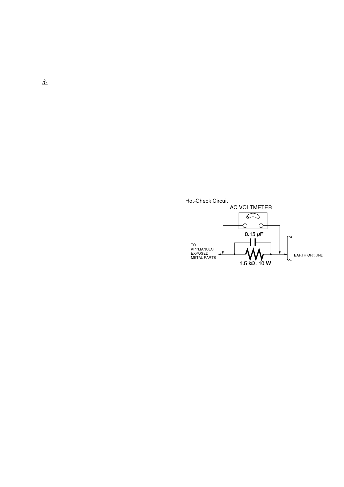
1.3. Leakage Current Hot Check (See Figure 1.) --------3
2Warning--------------------------------------------------------------4
2.1. Prevention of Electrostatic Discharge (ESD)
to Electrostatically Sensitive (ES) Devices ----------4
2.2. How to Recycle the Lithium Ion Battery (U.S.
Only)-----------------------------------------------------------4
2.3. Caution for AC Cord (For EB/GC) ---------------------5
2.4. How to Replace the Lithium Battery -------------------6
3 Service Navigation------------------------------------------------7
3.1. Introduction --------------------------------------------------7
3.2. General Description About Lead Free Solder
(PbF) ----------------------------------------------------------7
3.3. Important Notice 1:(Other than U.S.A. and
Canadian Market) ------------------------------------------7
3.4. How to Define the Model Suffix (NTSC or PAL
model)---------------------------------------------------------8
3.5. Formatting----------------------------------------------------9
4 Specifications ---------------------------------------------------- 10
5 Location of Controls and Components------------------ 12
6 Service Mode ----------------------------------------------------- 14
6.1. History Display -------------------------------------------- 15
7 Service Fixture & Tools --------------------------------------- 16
7.1. When Replacing the Main P.C.B. -------------------- 16
7.2. Service Position ------------------------------------------ 16
8 Disassembly and Assembly Instructions --------------- 17
8.1. Disassembly Flow Chart for the Unit ---------------- 17
8.2. PCB Location---------------------------------------------- 17
8.3. Disassembly Procedure for the Unit ---------------- 17
9 Measurements and Adjustments -------------------------- 24
9.1. Electric Adjustment --------------------------------------24
10 Factory Setting--------------------------------------------------- 26
10.1. How To Turn On The Factory Settings? ------------ 26
10.2. What Is The Factory Settings? ----------------------- 26
11 Block Diagra m --------------------------------------------------- 27
11.1. Overall Block Diagram ----------------------------------27
11.2. Camera/System Control Circuit Block
Diagram----------------------------------------------------- 28
11.3. Video/Audio Signal Process(1) Circuit Block
Diagram----------------------------------------------------- 29
11.4. Video/Audio Signal Process(2) Circuit Block
Diagram----------------------------------------------------- 30
11.5. Lens Drive Circuit Block Diagram -------------------- 31
11.6. Power Supply Circuit Block Diagram---------------- 32
12 Wiring Connection Diagram --------------------------------- 33
12.1. Interconnection Diagram ------------------------------- 33
2
1 Safety Precautions
1.1. General Guidelines
1. IMPORTANT SAFETY NOTICE There are special components used in this equipment which are important for safety. These parts are marked by
in the Schematic Diagrams, Circuit Board Layout,
Exploded Views and Replacement Parts List. It is essential that these critical parts should be replaced with manufacturer’s specified parts to prevent X-RADIATION,
shock, fire, or other hazards. Do not modify the original
design without permission of manufacturer.
2. An Isolation Transformer should always be used during
the servicing of AC Adaptor whose chassis is not isolated
from the AC power line. Use a transformer of adequate
power rating as this protects the technician from accidents resulting in personal injury from electrical shocks. It
will also protect AC Adaptor from being damaged by accidental shorting that may occur during servicing.
3. When servicing, observe the original lead dress. If a short
circuit is found, replace all parts which have been overheated or damaged by the short circuit.
4. After servicing, see to it that all the protective devices
such as insulation barriers, insulation papers shields are
properly installed.
5. After servicing, make the following leakage current
checks to prevent the customer from being exposed to
shock hazards.
1.3. Leakage Current Hot Check (See Figure 1.)
1. Plug the AC cord directly into the AC outlet. Do not use an isolation transformer for this check.
2. Connect a 1.5 kΩ, 10 W resistor, in parallel with a 0.15 μF
capacitor, between each exposed metallic part on the set
and a good earth ground, as shown in Figure 1.
3. Use an AC voltmeter, with 1 kΩ/V or more sensitivity, to
measure the potential across the resistor.
4. Check each exposed metallic part, and measure the voltage at each point.
5. Reverse the AC plug in the AC outlet and repeat each of
the above measurements.
6. The potential at any point should not exceed 0.75 V RMS.
A leakage current tester (Simpson Model 229 or equivalent) may be used to make the hot checks, leakage current must not exceed 1/2 mA. In case a measurement is
outside of the limits specified, there is a possibility of a
shock hazard, and the equipment should be repaired and
rechecked before it is returned to the customer.
1.2. Leakage Current Cold Check
1. Unplug the AC cord and connect a jumper between the two prongs on the plug.
2. Measure the resistance value, with an ohmmeter,
between the jumpered AC plug and each exposed metallic cabinet part on the equipment such as screwheads,
connectors, control shafts, etc. When the exposed metallic part has a return path to the chassis, the reading
should be between 1 MΩ and 5.2 MΩ. When the exposed
metal does not have a return path to the chassis, the
reading must be infinity.
Figure. 1
3
2Warning
2.1. Prevention of Electrostatic Discharge (ESD) to Electrostatically Sensitive (ES) Devices
Some semiconductor (solid state) devices can be damaged easily by static electricity. Such components commonly are called Electrostatically Sensitive (ES) Devices. Examples of typical ES devices are integrated circuits and some field-effect transistors and
semiconductor "chip" components. The following techniques should be used to help reduce the incidence of component damage
caused by electrostatic discharge (ESD).
1. Immediately before handling any semiconductor component or semiconductor-equipped assembly, drain off any ESD on your
body by touching a known earth ground. Alternatively, obtain and wear a commercially available discharging ESD wrist strap,
which should be removed for potential shock reasons prior to applying power to the unit under test.
2. After removing an electrical assembly equipped with ES devices, place the assembly on a conductive surface such as aluminum foil, to prevent electrostatic charge buildup or exposure of the assembly.
3. Use only a grounded-tip soldering iron to solder or unsolder ES devices.
4. Use only an antistatic solder removal device. Some solder removal devices not classified as "antistatic (ESD protected)" can
generate electrical charge sufficient to damage ES devices.
5. Do not use freon-propelled chemicals. These can generate electrical charges sufficient to damage ES devices.
6. Do not remove a replacement ES device from its protective package until immediately before you are ready to install it. (Most
replacement ES devices are packaged with leads electrically shorted together by conductive foam, aluminum foil or comparable conductive material).
7. Immediately before removing the protective material from the leads of a replacement ES device, touch the protective material
to the chassis or circuit assembly into which the device will be installed.
CAUTION :
Be sure no power is applied to the chassis or circuit, and observe all other safety precautions.
8. Minimize bodily motions when handling unpackaged replacement ES devices. (Otherwise harmless motion such as the
brushing together of your clothes fabric or the lifting of your foot from a carpeted floor can generate static electricity (ESD) sufficient to damage an ES device).
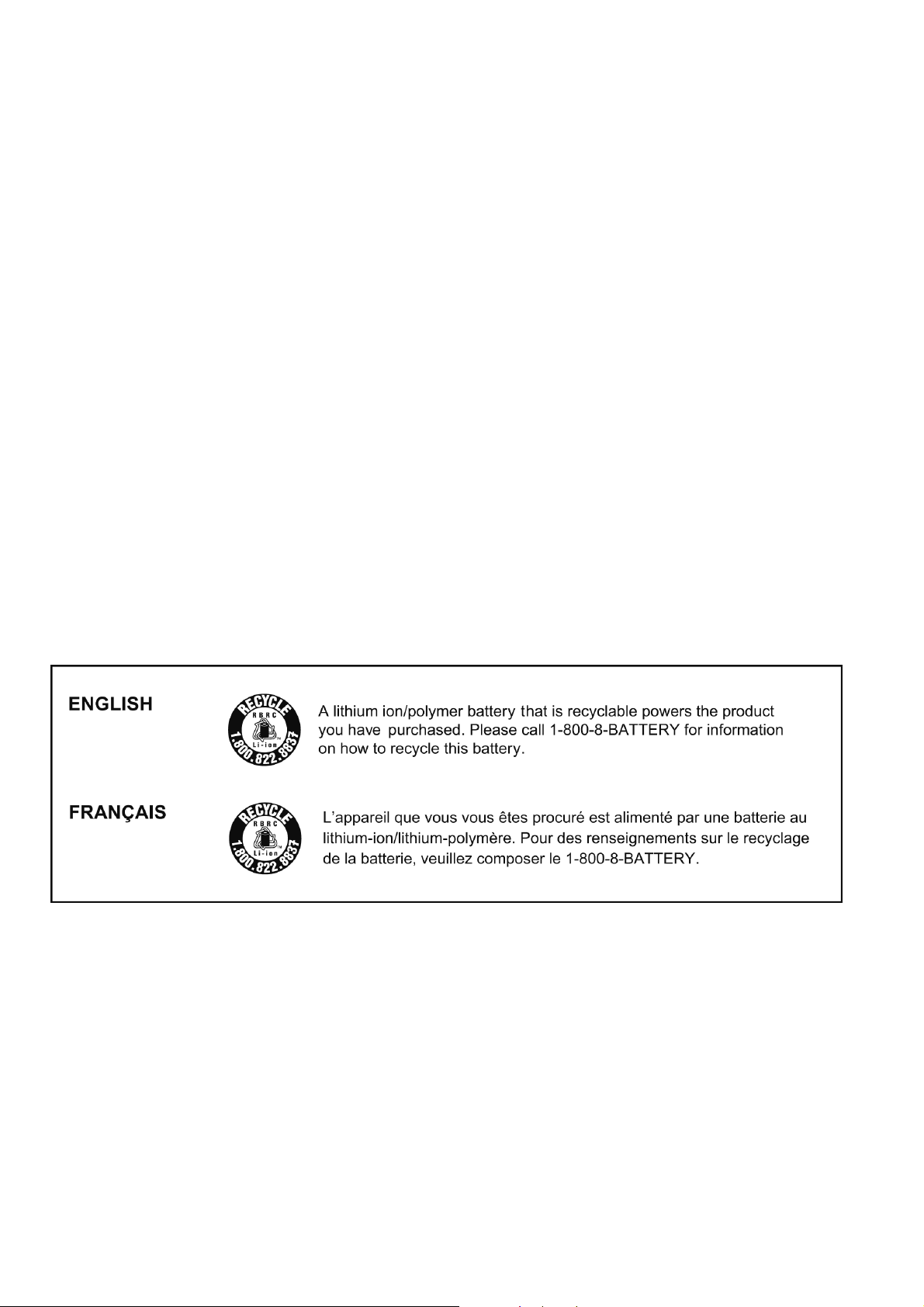
2.2. How to Recycle the Lithium Ion Battery (U.S. Only)
4
2.3. Caution for AC Cord (For EB/GC)
2.3.1. Information for Your Safety
IMPORTANT
Your attention is drawn to the fact that recording of prerecorded tapes or discs or other published or broadcast
material may infringe copyright laws.
WARNING
To reduce the risk of fire or shock hazard, do not expose
this equipment to rain or moisture.
CAUTION
To reduce the risk of fire or shock hazard and annoying
interference, use the recommended accessories only.
FOR YOUR SAFETY
DO NOT REMOVE THE OUTER COVER
To prevent electric shock, do not remove the cover. No user
serviceable parts inside. Refer servicing to qualified service
personnel.
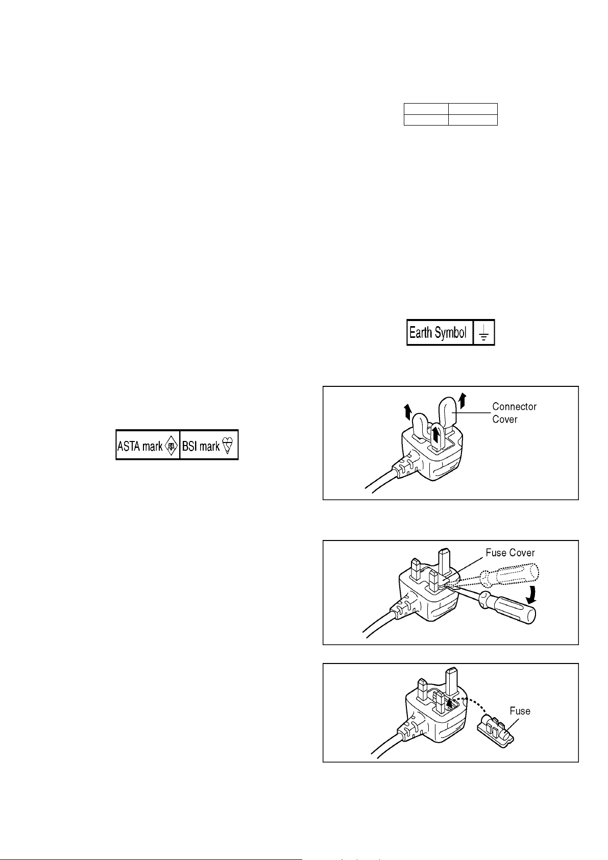
2.3.2. Caution for AC Mains Lead
For your safety, please read the following text carefully.
This appliance is supplied with a moulded three-pin mains plug
for your safety and convenience.
A 5-ampere fuse is fitted in this plug.
Should the fuse need to be replaced please ensure that the
replacement fuse has a rating of 5 amperes and it is approved
by ASTA or BSI to BS1362
Check for the ASTA mark or the BSI mark on the body of the
fuse.
2.3.2.1. Important
The wires in this mains lead are coloured in accordance with
the following code:
Blue Neutral
Brown Live
As the colours of the wires in the mains lead of this appliance
may not correspond with the coloured markings identifying the
terminals in your plug, proceed as follows:
The wire which is coloured BLUE must be connected to the terminal in the plug which is marked with the letter N or coloured
BLACK.
The wire which is coloured BROWN must be connected to the
terminal in the plug which is marked with the letter L or coloured
RED.
Under no circumstances should either of these wires be connected to the earth terminal of the three pin plug, marked with
the letter E or the Earth Symbol.
2.3.2.2. Before Use
Remove the Connector Cover as follows.
If the plug contains a removable fuse cover you must ensure
that it is refitted when the fuse is replaced.
If you lose the fuse cover, the plug must not be used until a
replacement cover is obtained.
A replacement fuse cover can be purchased from your local
Panasonic Dealer.
If the fitted moulded plug is unsuitable for the socket outlet in
your home then the fuse should be removed and the plug cut
off and disposed of safety.
There is a danger of severe electrical shock if the cut off plug is
inserted into any 13-ampere socket.
If a new plug is to be fitted please observe the wiring code as
shown below.
If in any doubt, please consult a qualified electrician.
2.3.2.3. How to Replace the Fuse
1. Remove the Fuse Cover with a screwdriver.
2. Replace the fuse and attach the Fuse cover.
5
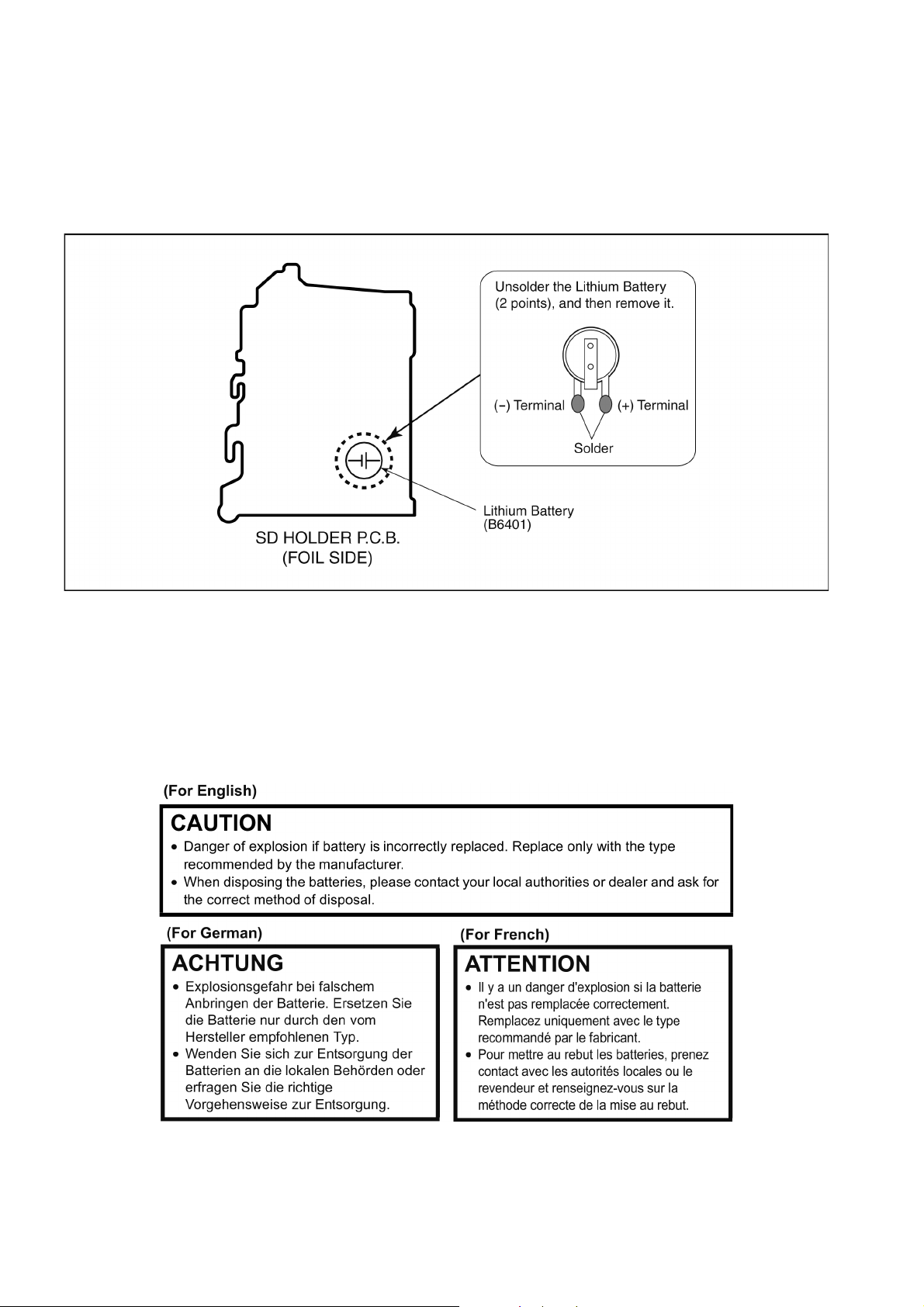
2.4. How to Replace the Lithium Battery
2.4.1. Replacement Procedure
1. Remove the SD Holder P.C.B.. (Refer to Disassembly Procedures.)
2. Unsolder the each soldering point of electric lead terminal for Lithium battery (Ref. No. “B6401” at foil side of SD HOLDER
P.C.B.) and remove the Lithium battery together with electric lead terminal. Then replace it into new one.
NOTE:
The Type No. ML-614S/DN includes electric lead terminals.
NOTE:
This Lithium battery is a critical component.
(Type No.: ML-614S/DN Manufactured by Energy Company, Panasonic Corporation)
It must never be subjected to excessive heat or discharge.
It must therefore only be fitted in requirement designed specifically for its use.
Replacement batteries must be of same type and manufacture.
They must be fitted in the same manner and location as the original battery, with the correct polarity contacts observed.
Do not attempt to re-charge the old battery or re-use it for any other purpose.
It should be disposed of in waste products destined for burial rather than incineration.
NOTE:
Above caution is applicable for a battery pack which is for HC-V100/V100M series, as well.
6
3 Service Navigation
3.1. Introduction
This service manual contains technical information, which allow service personnel’s to understand and service this model.
Please place orders using the parts list and not the drawing reference numbers.
If the circuit is changed or modified, the information will be followed by service manual to be controlled with original service manual.
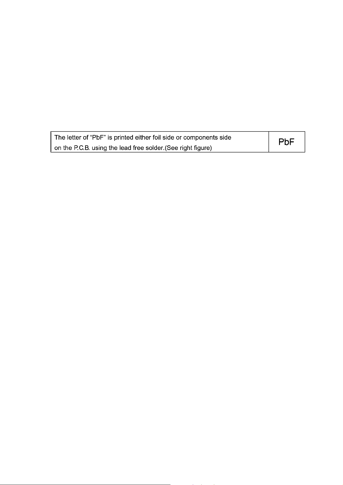
3.2. General Description About Lead Free Solder (PbF)
The lead free solder has been used in the mounting process of all electrical components on the printed circuit boards used for this
equipment in considering the globally environmental conservation.
The normal solder is the alloy of tin (Sn) and lead (Pb). On the other hand, the lead free solder is the alloy mainly consists of tin
(Sn), silver (Ag) and Copper (Cu), and the melting point of the lead free solder is higher approx.30°C (86°F) more than that of the
normal solder.
Distinction of P.C.B. Lead Free Solder being used
Service caution for repair work using Lead Free Solder (PbF)
• The lead free solder has to be used when repairing the equipment for which the lead free solder is used.
(Definition: The letter of “PbF” is printed on the P.C.B. using the lead free solder.)
• To put lead free solder, it should be well molten and mixed with the original lead free solder.
• Remove the remaining lead free solder on the P.C.B. cleanly for soldering of the new IC.
• Since the melting point of the lead free solder is higher than that of the normal lead solder, it takes the longer time to melt the
lead free solder.
• Use the soldering iron (more than 70W) equipped with the temperature control after setting the temperature at 350±30°C
(662±86°F).
Recommended Lead Free Solder (Service Parts Route.)
• The following 3 types of lead free solder are available through the service parts route.
RFKZ03D01KS-----------(0.3mm 100g Reel)
RFKZ06D01KS-----------(0.6mm 100g Reel)
RFKZ10D01KS-----------(1.0mm 100g Reel)
Note
* Ingredient: tin (Sn) 96.5%, silver (Ag) 3.0%, Copper (Cu) 0.5%, Cobalt (Co) / Germanium (Ge) 0.1 to 0.3%
3.3. Important Notice 1:(Other than U.S.A. and Canadian Market)
1. The service manual does not contain the following information, because of the impossibility of servicing at component level
without concerned equipment/facilities.
a. Schematic diagram, Block Diagram and P.C.B. layout of MAIN P.C.B..
b. Parts list for individual parts for MAIN P.C.B..
When a part replacement is required for repairing MAIN P.C.B., replace as an assembled parts. (Main P.C.B.)
2. The following category is /are recycle module part. Please send it/them to Central Repair Center.
• MAIN P.C.B. (VEP03J56CN: HC-V100P/PC/PU)
• MAIN P.C.B. (VEP03J56CP: HC-V100EB/EC/EE/EF/EG/EP/GC/GK/GN/GW)
• MAIN P.C.B. (VEP03J56AN: HC-V100MP/PC/PU)
• MAIN P.C.B. (VEP03J56AP: HC-V100MGK)
7

3.4. How to Define the Model Suffix (NTSC or PAL model)
There are seven kinds of HC-V100/V100M.
• a) HC-V100M (Japan domestic model)
• b) HC-V100P, V100MP
• c) HC-V100PC, V100MPC
• d) HC-V100EB/EC/EF/EG/EP/GN
• e) HC-V100EE
• f) HC-V100GK, V100MGK
• g) HC-V100PU/GC/GW, V100MPU
What is the difference is that the “INITIAL SETTING” data which is stored in Flash ROM mounted on Main P.C.B..
3.4.1. Defining methods:
To define the model suffix to be serviced, refer to the rating label and caution label which are putted on the Unit.
NOTE:
After replacing the MAIN P.C.B., be sure to achieve adjustment.
The adjustment instruction is available at “software download” on the “Support Information from NWBG/VDBG-AVC” web-site in
“TSN system”, together with Maintenance software.
8
3.5. Formatting
9
4 Specifications
10
11
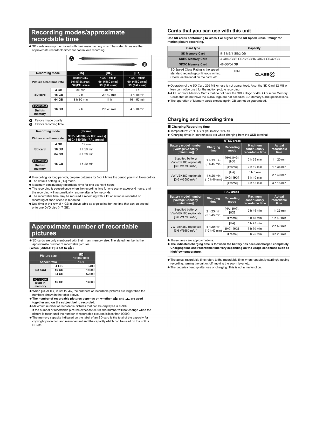
5 Location of Controls and Components
1 Speaker
2 USB terminal [ ]
3 Intelligent auto/Manual button
[iA/MANUAL]
4 Optical image stabilizer/Delete button
[ O.I.S./ ]
5 Power button [ ]
6 HDMI mini connector [HDMI]
7 AV multi connector [AV MULTI]
●
Use the AV multi cable (only the supplied
cable).
8 Battery release lever [BATT]
9 Lens cover opening/closing switch
When not using the unit, close the lens
cover to protect the lens.
●
Slide the opening/closing switch to
open/close the cover.
10 Lens cover
11 Lens
12 Internal stereo microphones
AV MULTI
1
3
4
5
867
2
9
11
12
13 Menu button [MENU]
14 Mode switch
15 Status indicator
16 Recording start/stop button
17 Cursor button
●
Use the cursor button to select the
recording functions and playback
operations, and to operate the menu
screen.
18 Enter button [ENTER]
19 LCD monitor
●
It can open up to 90Q.
●
It can rotate up to 180Q towards the lens
or 90Q towards the opposite direction.
20 Battery holder
1413
15 16
20718191
Due to limitations in LCD production
technology, there may be some tiny bright
or dark spots on the LCD monitor screen.
However, this is not a malfunction and
does not affect the recorded picture.
10
12
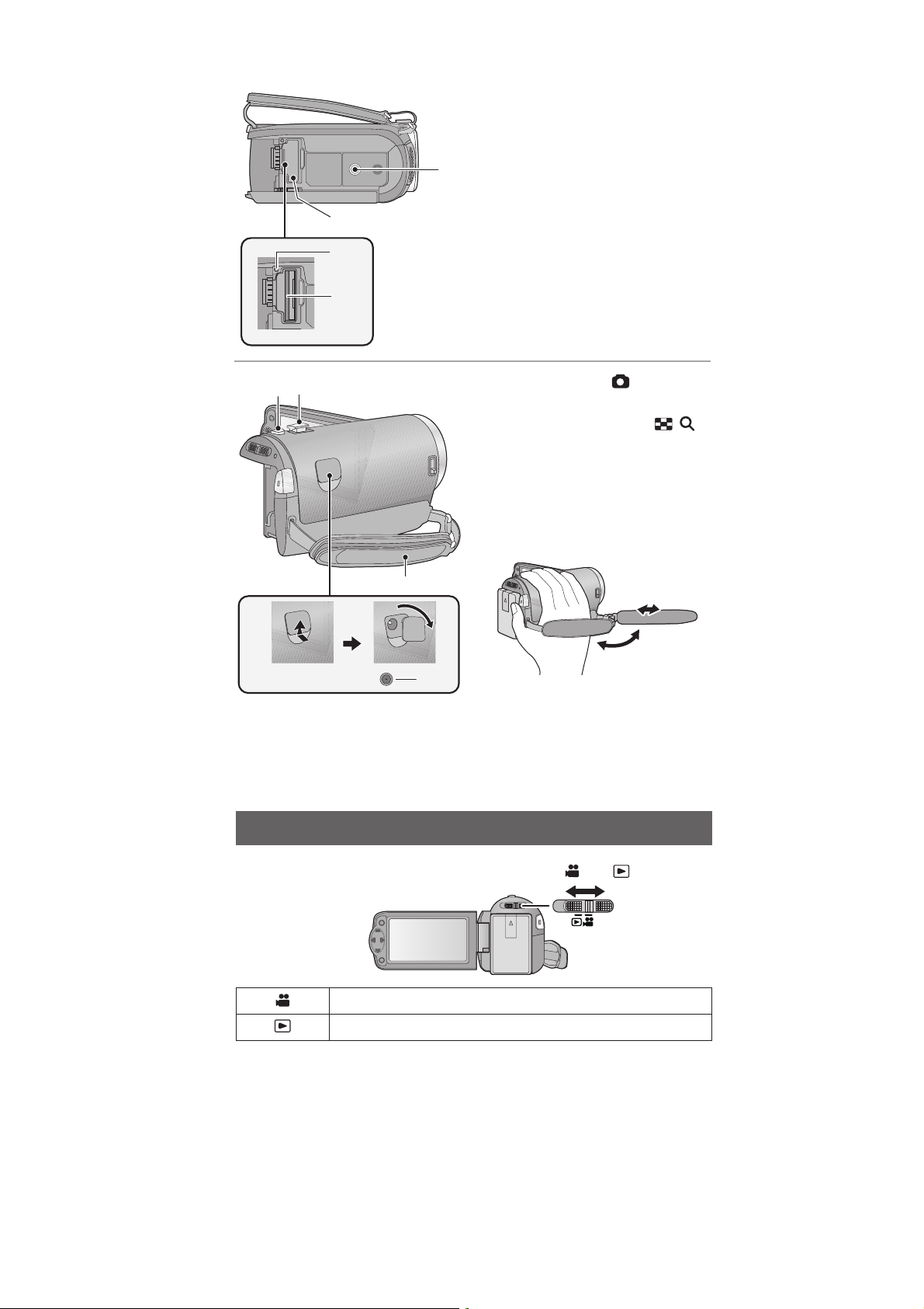
21 Tripod receptacle
●
If you attach a tripod which has a 5.5 mm
(0.22 S) screw or larger, it may damage
this unit.
22 SD card cover
23 Access lamp [ACCESS]
24 Card slot
25 Photoshot button [ ]
26 Zoom lever [W/T] (In Recording
Mode)
Thumbnail display switch [ / ]/
Volume lever [UVOLT] (In Playback
Mode)
27 DC input terminal [DC IN]
●
Do not use any other AC adaptors except
the supplied one.
28 Grip belt
Adjust the length of the grip belt so that it fits
your hand.
Flip the belt.
Adjust the length.
Replace the belt.
21
Change the mode to recording or playback.
Operate the mode switch to change the mode to or .
Selecting a mode
Recording Mode
Playback Mode
22
23
24
5262
28
27
13
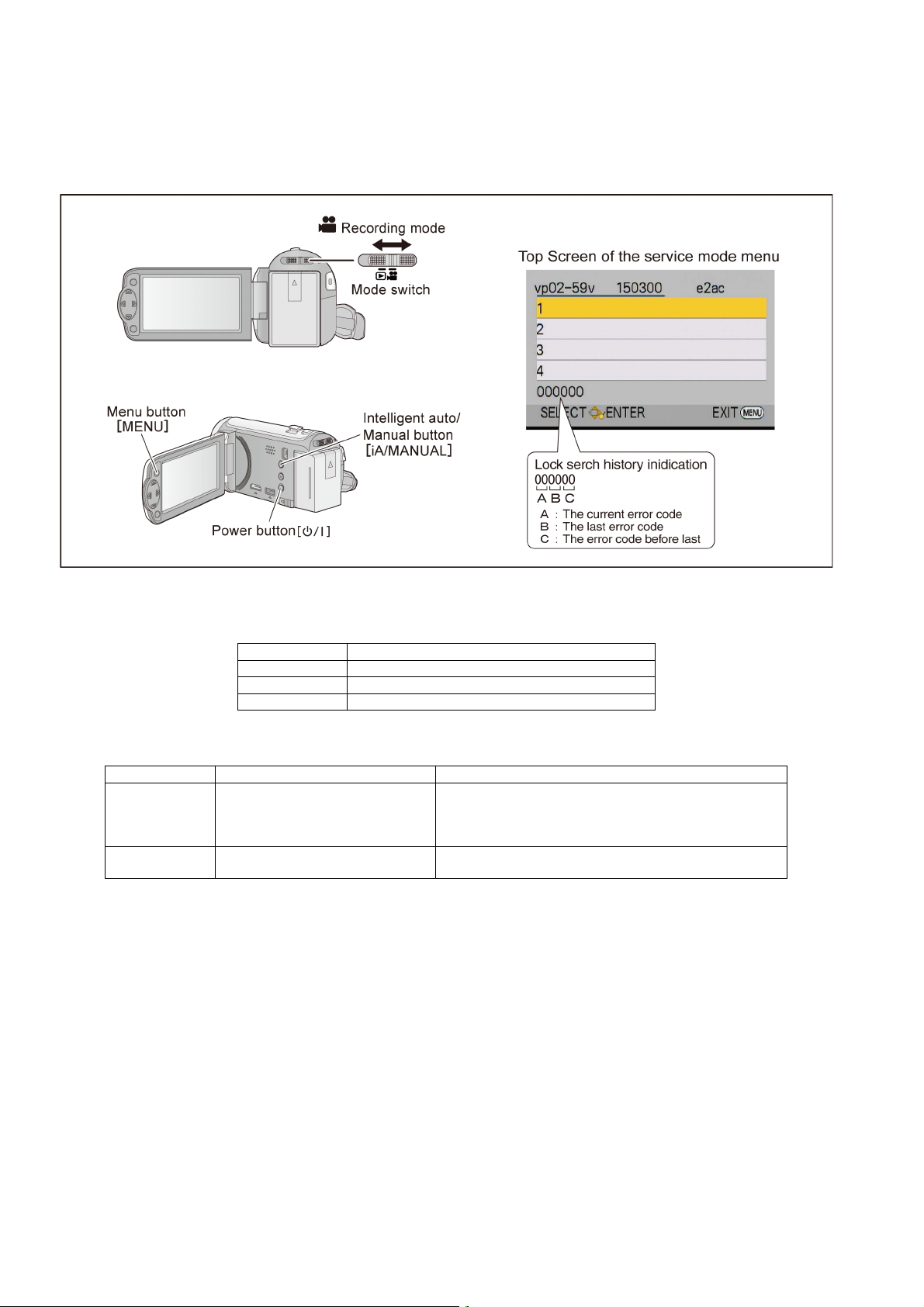
6 Service Mode
1. Indication method of the service menu Set the mode switch “Recording” mode.
2. Turn the power on, and then while keep pressing the “Zoom lever” to W side, “Intelligent auto/Manual” button and “Menu” button for more than 3 seconds until the top screen of the Service Mode Menu being displayed.
Lock search history indication
• Display the camera system error cord for three histories saved in EEPROM
• The error cord contents which are displayed
Error code Function
51 Focus control is abnormal
52 Zoom control is abnormal
53 OIS lens control is abnormal
Service mode menu
Screen display Contents Function
1 Factory settings Function to throw a product up in a factory shipment state
(Even if recorded data exists in the build-in memory, factory
settings perform the initialization of build-in memory and clear
the history data.)
4 History display Display accumulated operating time, total recording time and
accumulated number of photos taken.
NOTE:
Do not using service mode except above table of Service mode menu.
3. End method of the top screen of the service mode menu
Press the [MENU] button to end the service mode, and then POWER OFF.
14
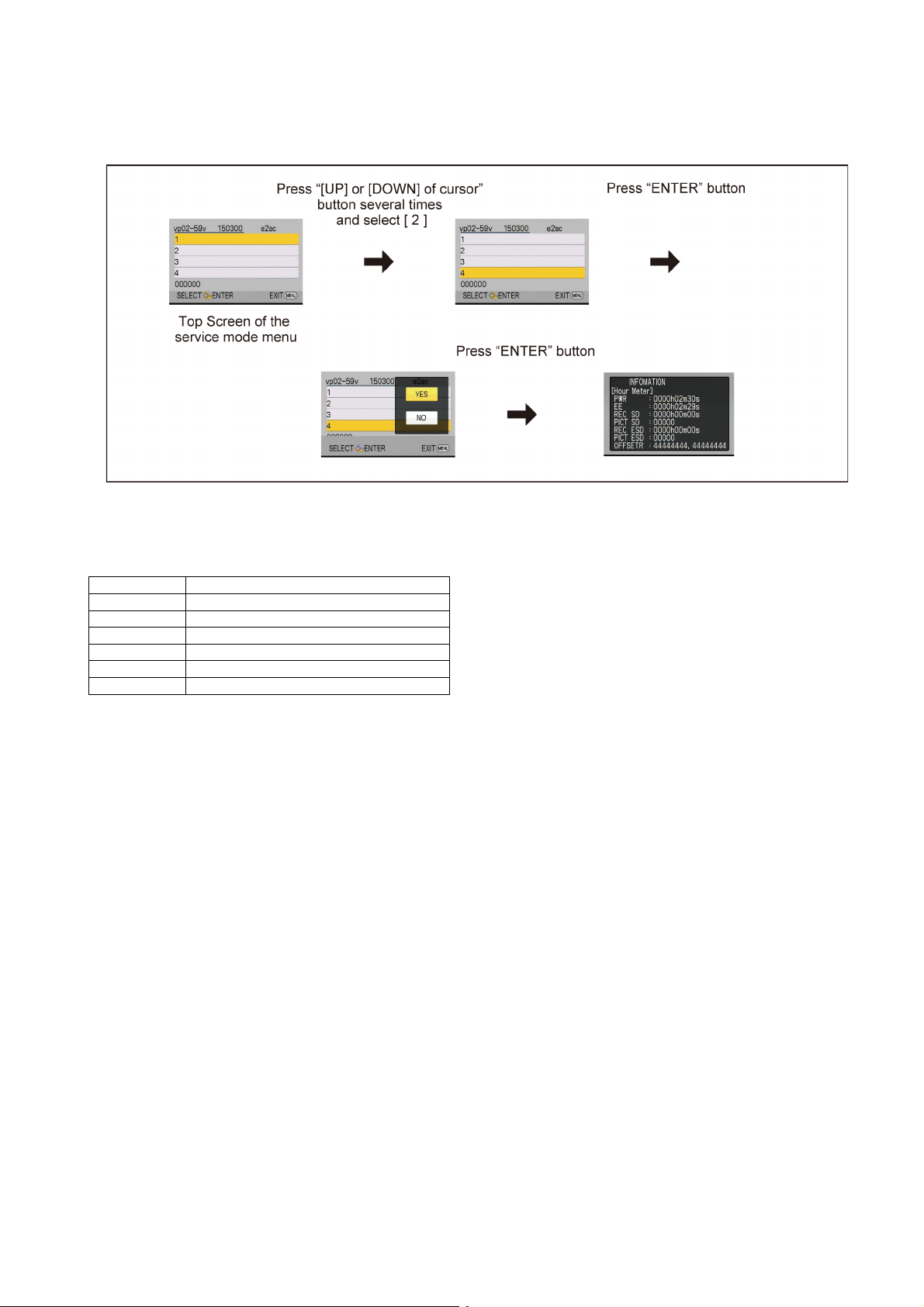
6.1. History Display
Press the “[UP] or [DOWN] of cursor” button for the item No. [4] is yellow high lighted, then press “ENTER” button to display the unit
histories.
Operation specifications
Indication contents
• Display the total operating time (in power on and EE state), total movie recording time and total number of photo taken. (They are
stored in EEPROM).
Item Contents
PWR Total elapsed time
EE Total working time of camera sensor
REC SD Movie recorded time of inserted SD card
PICT SD Picture recorded number of inserted SD card
REC ESD Movie recorded time of internal memory
PICT ESD Picture recorded number of internal memory
Press “MENU” button then return to normal recording mode.
15

7 Service Fixture & Tools
7.1. When Replacing the Main P.C.B.
After replacing the MAIN P.C.B., be sure to achieve adjustment.
The adjustment instruction is available at “software download” on the “Support Information from NWBG/VDBG-AVC” web-site in
“TSN system”, together with Maintenance software.
7.2. Service Position
This Service Position is used for checking and replacing parts. Use the following Extension cables for servicing.
Table S1 Extension Cable List
No. Parts No. Connection Form
1 RFKZ0487 FP6004(MAIN) - MONITOR FPC 35PIN 0.3 FFC
2 RFKZ0444 PP6001(MAIN) - PS6401(SD HOLDER) 50PIN 0.5 B to B
3 VFK1480 FP6003(MAIN) - ECM FPC(FRONT CASE UNIT) 6PIN 0.5 FFC
4 VFK1440 FP6402(SD HOLDER) - TOP OPERATION UNIT(SIDE CASE-R UNIT) 10PIN 0.5 FFC
16
8 Disassembly and Assembly Instructions
8.1. Disassembly Flow Chart for the Unit
This is a disassembling chart.
When assembling, perform this chart conversely.
8.2. PCB Location
8.3. Disassembly Procedure for the Unit
No. Item Fig Removal
1 Top Case Unit Fig. D1 1 Screw (A)
Fig. D2 2 Screws (B)
3 Locking tabs
3 Hooking parts
Top Case Unit
2 Side Case L Unit Fig. D3 1 Screw (C)
4 Screws (D)
Fig. D4 2 Locking tabs
1 Convex
1 Projection part
Side Case L Unit
3 Front Case Unit Fig. D5 1 Screw (F)
1 Screw (G)
Fig. D6 FP6003 (Flex)
1 Rib
Front Case Unit
4 Lens Unit Fig. D7 FP6008 (Flex)
Fig. D8 PP301 (Connector)
1 Convex
Lens Unit
5 Main P.C.B.
SD Holder P.C.B.
6 ESD P.C.B.
(HC-V100M only)
7 LCD Case T Unit
LCD Unit
Fig. D9 5 Screws (H)
FP6004 (Flex)
P6003 (Connector)
P6401(Connector)
FP6402(Flex)
2 Ribs
FP3201 (Flex)
Fig. D10 NOTE: (When Installing)
Fig. D11 SD Holder P.C.B.
Main P.C.B.
Fig. D12 2 Screws (I)
ESD P.C.B.
Fig. D13 2 Screws (J)
2 Screws (K)
Fig. D14 7 Locking tabs
LCD Case T Unit
FP901 (Flex)
1 Screw (L)
1 Hooking part
LCD Unit
17
8.3.1. Removal of the Top Case Unit
Fig. D2
Fig. D1
18
8.3.2. Removal of the Side Case L Unit
Fig. D3
Fig. D4
8.3.3. Removal of the Front Case Unit
19
Fig. D5
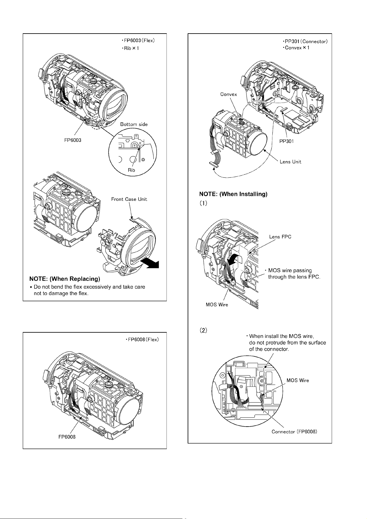
Fig. D6
8.3.4. Removal of the Lens Unit
Fig. D7
Fig. D8
20

8.3.5. Removal of the Main P.C.B. and SD Holder P.C.B.
Fig. D9
Fig. D10
21

8.3.7. Removal of the LCD Case T Unit and LCD Unit
Fig. D11
8.3.6. Removal of the ESD P.C.B. Unit (HC-V100M only)
Fig. D13
Fig. D12
22

Fig. D14
23

9 Measurements and Adjustments
9.1. Electric Adjustment
• Adjustment method is different from a conventional High definition video camera.
• An exclusive jig and PC (including software for adjustment “Tatsujin”) are necessary for electric adjustment.
• A USB driver for service is necessary to communication with PC.
• Connection method of the main unit and an exclusive adjustment jig as follows
9.1.1. Adjustment Procedure
• Connect the main unit to PC with USB.
The adjustment instruction is available at "Software download" on the "Support Information from NWBG/VDBG-AVC" web-site in
"TSN System".
Figure of connection
Figure of image when adjustment
Part Number of jig
• Only a necessary jig mentions it in setup of electric adjustment.
No. Part Name Part Number Remarks
1 PC -----2 AC Adaptor -----3 USB Cable -----4 Adjustment Software (Tatsujin) -----5 C4 Filter VFK1164LBB4 The same as C12 Filter (VFK1164LBB12).
6 C8 Filter VFK1164LBB8
24

Adjustment Items
• Adjustment item as follows.
The adjustment instruction is available at "Software download" on the "Support Information from NWBG/VDBG-AVC" web-site in
"TSN System".
25

10 Factory Setting
10.1. How To Turn On The Factory Settings?
(CAUTION)
Performing the factory settings, the built-in memory is initialized and all of recorded data are deleted.
(SD memory card is not initialized by the factory settings.)
1. Set the mode switch “Recording” mode.
2. Turn the power on, and then while keep pressing the “Zoom lever” to W side, “Intelligent auto/Manual” button and “Menu” button for more than 3 seconds until the top screen of the Service Mode Menu being displayed.
3. Under the condition of the Item No. [ 1 ] is yellow high lighted , then press “ENTER” button.
4. By pressing the “[UP] or [DOWN] of cursor” button and display a highlight in a [ YES ] item, then press the “ENTER” button.
5. After few seconds “END” is displayed on LCD monitor. Press [ POWER ] button or cutting of battery connection or AC power
supply connection as a completion of the “FACTORY SETTINGS”.
NOTE:
Do not using service mode except above table of Service mode menu.
End method of the top screen of the service mode menu.
Push the “MENU” button to end the service mode, and then POWER OFF.
10.2. What Is The Factory Settings?
The factory settings clean up and/or refresh the following settings.
1. Physical formatting of the built-in memory. (All user recorded data are deleted)
2. MENU, MODE, ADJUSTMENT VALUE.
3. Reset the folder number and file number of still pictures.
(Setting the folder number is 100, and file number is 0.)
4. Clear the service mode information contents.
5. Initialize the VIERA Link Physical Address.
The setting position of factory settings:
Name Setting position
Mode switch Recording mode
26

10 Block Diagram
OVERALL BLOCK DIAGRAM
IRIS
IC701
LENS/OIS DRIVE
SD
CARD
SPEAKER
ECM
DC IN
BATTERY
SHUTTER
IC201
MOS IMAGE
SENSOR
HDMI mini
CONNECTOR
ZOOM/
FOCUS
MOTOR/
OIS
Analog
Analog
IC6401
GYRO
SENSOR
IC3404
NAND
FLASH ROM/
512Mbit
IC3401
ASIC
IC1001
POWER
IC1502
BATTERY
MONITOR
NOTE
: VIDEO SIGNAL
: AUDIO SIGNAL
: CLK or CONTROL LINE
X3401
OSC
(48MHz)
COLOR LCD
PANEL
IC3751
VIDEO
ENCODER
IC3701
VIDEO
AMP
IC3202
INTERNAL MEMORY
/16GB
X2303
(32.768kHz)
IC1503
RTC/CHARAGE/
POWER CONTROL
USB TERMINAL
IC301,703,704,1011,
1421,1441,1471
REGULATOR
HC-V100M/V100 OVERALL BLOCK DIAGRAM
HC-V100M ONLY
IC3403
DDR3 SDRAM/
512Mbit
IC3402
DDR3 SDRAM/
512Mbit
A/V
MULTI
TERMINAL
Analog
Analog
OPERATION
IC2006
SYSTEM CONTROL
(CAMERA MICROCOMPUTER)
IC2002
EEPROM
X2001
OSC
(13.5MHz)
IC202,302
GATE IC
IC705
D-TYPE
FLIP-FLOP
IC511
MAGNETIC
SENSOR
IC2301
RESET
IC1501
VOLTAGE
DET.
LENS(F1.8 4.0 34x)
10.1. Overall Block Diagram
27

10.2. Camera/System Control Circuit Block Diagram
IC2006
(SYSTEM CONTROL)
CAMERA/SYSTEM CONTROL CIRCUIT BLOCK DIAGRAM
X2303
(32.768kHz)
S6001
LCD OPEN/CLOSE
CARD LED B
KEYIN4
POWER LED B
D6451
CARD
LED
PW REG3V
QR6402
PW 3.2V
PW REG3V
G19
QR6002
PW 3.2V
STANDBYLED B
U5
QR6003
G20
C6
QR6007
KEYIN1
D6
U3
IC1503
(RTC/CHARGE/POWER CONTROL)
S6401
POWER ON/OFF
D3
G5
G6
/SWIN1
E3
/SWIN2
XIN
XOUT
A5
LED
IC511
(MAGNETIC SENSOR)
4
3
1
2
VDD
OUT
GND
NC
HC-V100M/V100 CAMERA/SYSTEM CONTROL CIRCUIT BLOCK DIAGRAM
LCD RVS
CHA DI
CHA
DO
CHA SCK
CHA CS
D15
A16
B15
B16
B6
CS
B7
SCK
C6
SDI
C7
SDO
QR2002
PW RTCVREG32
ZSW
(To IC701-49)
IC201
(MOS IMAGE SENSOR)
A15
GPIOF38
GPIOF39
SCKIN0
SCKIP0
GPIOF37
GPIOF36
A14
A17
5
1
4
32
IC302
(GATE IC)
CH202
CH205 CH206
CH203
CH201
CH302
CH303
CH2004
CH2005 CH2006
CH207
PW SENS1.8V
63
53
62
DOAM
DOAP
DCKM
A16
A18
A19
64
55
54
DCKP
DOBP
DOBM
RL3431
RL3434 RL3433
RL3432
ADCK
K19
TGVD
ZMRST
GPIOF4
PLLEN
GPIOF18
GPIOC6
GPIOF16
GPIOF15
GPIOF7
GPIOF1
GPIOF11
GPIOF6
GPIOF9
GPIOF10
H19
BUS240 DAM
BUS240 DAP
BUS240 CKM
BUS240 CKP
BUS240 DBP
BUS240 DBM
49
XVS
XVD CAM
TGHD
J19
42
XHS
XHD CAM
GPIOC10
AA1
35
SDI
S SENS SDO
GPIOC11
W2
36
SCK
S SENS SCK
GPIOC12
Y1
14
XCE
S SENS CS
GPIOC9
Y2
22
XCLR
E MOS RST
CLK60 MOS
BUS240 DOAM
BUS240 DOAP
BUS240 DCKM
BUS240 DCKP
BUS240 DOBP
BUS240 DOBM
VD
HD
SDI
SCK
SCS
SI SYS2
Y11
S SYS2 BS
SO SYS2
V11
S SYS2 SB
CLK SYS2
W11
E20
AC1
E18
S SYSY2 SCK
R0410L 00H
V6
R0410L 00H
BE REQ2
Y5
BE REQ2
SYS REQ2
Y6
C10
E14
C18
SYS REQ2
COMP BOOT
E2
COMP BOOT
BE UPDATE
U8
BE UPDATE
CAM UPDATE
W8
E15
E16
C13
CAM UPDATE
DDR COMP CAL
V8
DDR COMP CAL
PLL EN
Y8
E PLL EN
BE RST
E1
C15
B20
C20
E BE RST
NTSC L PAL H
TGHD SYNC
H3
TGHD SYNC H
C12
RSTN
50
INCK
5
1
4
32
IC202
(GATE IC)
PW MOS1.8V
CH204
TOP OPERATION UNIT
FP6402
ZOOMAD
1
2
4
5
6
7
POWER LED
8
STANDBY LED
AVREF
AVREF
VTR KEY 1
PW REG3V
S6404
S/S SW
S6403
IA
S6402
OIS
MODE SWITCH
ZOOM LEVER
PHOTO SHOT BUTTON
IC3401
(ASIC)
IC2002
(EEPROM)
5
1
2
/CS
DI
DO
EEPROM DI
EEPROM DO
EEPROM CS
6
3
SK
WP
EEPROM SCK
EEPROM WP
7
/HOLD
CK2003
CK2004
CK2006
CK2007
CK2005
CL2008
CL2011
CL2009
CL2010
CL2013
CK2002
CL2012
8
VCC
GPIOF8
NTSC PAL
D12C14
PW REG3V
B13
C15
A15
C13
B14
Q2001
CL3405
CL3404
X2001
(13.5MHz)
K1
L1
OSC IN
OSC OUT
PHOTO2 ZENOSHI
PHOTO ZENOSI
F2
QR6008
KEYIN6
MENU
FP503
KEYIN6
3
LCD OP FPC
C5
ENTER
XI
XO
X3401
(48MHz)
C25
D25
CH301
P LED ON L
S RTC DI
S RTC DO
S RTC SCK
RTC CS
POWER SW
E LCD OPEN
28

10.3. Video/Audio Signal Process(1) Circuit Block Diagram
VIDEO/AUDIO SIGNAL PROCESS(1)CIRCUIT BLOCK DIAGRAM
IC3402/3403
(DDR3 SDRAM/1G-bit)
IC3402 ONLY IC3403 ONLY
DATA
A3
E3
G3 F3 B7 C7
E7 D3
DATA
A3
E3
G3 F3 B7 C7
CTL SIG
E7 D3
L2
K7 K9J7J3 K3 L3
M3 N8 M2 T2 K1
IC3404
(NAND FLASH ROM/512M-bit)
ADDRESSCTL SIG CTL SIG
N7
N3
45 48 49
DATA
51 54
CTL SIG
8
11 13
9 15 16
ECM[L]
ECM[R]
HS3901
(SD CARD CONNECTOR)
C.DET
14
11
13
HC-V100M only
IC3202
(INTERNAL MEMORY/16GB)
JK6402
USB TERMINAL
D-
D+
CAMERA SECTION
1 MOS
SENSOR
RL4802
M4801
+
-
RL4801
RL4804
M4802
+
-
RL4803
SPEAKER
CMD
CLK
2
3
D0
D1
D2
D3
WP
7
8
9
1
2
5
10
12
A3
DAT0
A4
DAT1
A5
DAT2
B2
DAT3
CLK
M6
M5
CMD
PW REG3V
MIC AMP
Q4801-4803
BUS240 DAP
BUS240 DAM
BUS240 DBP
BUS240 DBM
BUS240 CKP
BUS240 CKM
IC3401
(ASIC)
CD0
U3
CD1
V1
U2
CD2
V3
CD3
CMD
T2
SDCLK
T1
U5
CDT
WP
U1
AB2
GPIOC0
GPIOC1
AA3
Y5
GPIOC2
Y3
GPIOC3
AA2
GPIOC7
GPIOC4
W5
DM
M25
N25
DP
A14
GPIOF39
GPIOF38
A15
A18
GPIOF37
A19
GPIOF36
A16
SCKIP0
A17
SCKIN0
MICLIN0/DMD
E1
F1
MICRIN0/DMC
K1
SPKP
L1
SPKN
AC8
DQ0
AD6
DQ15
DQSN0
AE3
AE4
DQSP0
AE7
DQSN1
AE6
DQSP1
AA9
DQM0
AC4
DQM1
DQ31
DQ16
AC17
AC21
AE17
DQSN2
AE18
STREAM CONTROL
CAMERA
DSP
DQSP2
DQSN3
DQSP3
DQM2
AD19
AD21
AE22
AE21
MEMORY CONTROL
DQM3
AE14
DCKP
AE16 AC15
DCKN
DCKE
AA15
ZDCS
ZRAS
AE8 AD9 AE9
ZCAS
ZDWE
DBA2
AD14
AD12
H.264
MPEG2
JPEG
AC3/5.1CH
PROCESSOR
DBA1
AA13
DBA0
ZDRSTW8ODT
AD17
AD10
DA0
DA12
AC14
HDMI DMA I/F
CAMERA SIGNAL PROCESSOR
AUDIO DSP
V24
D7
D0
Y25
GPIOA3
N23
MAIN CPU
ZWE
GPIOA1
M23
AB25
HDMI
CONTROL
AC25
ZRE
V25 L23
ZCS
GPIOA0
SCL
SDA
HPD
CEC
TX2P
TX2N
TX1P
TX1N
TX0P
TX0N
TXCP
TXCN
LCDCK1
GPIOE21
GPIOE22
GPIOE23
GPIOE24
GPIOE25
GPIOE26
GPIOE27
GPIOE28
GPIOE19
GPIOE20
GPIOC15
GPIOC13
GPIOC14
GPIOC8
LOUT
ROUT
VBO
GPIOE11
GPIOE18
GPIOE0
GPIOE7
LCDCK0
GPIOE8
GPIOE9
GPIOB0
GPIOB1
GPIOA20
GPIOA19
H23
G23
J23
F23
F24
F25
G24
G25
H24
H25
J24
J25
A7
B6
B7
A4
A5
C6
C7
C8
C9
B4
B5
V5
V2
W1
AB1
H3
J3
L3
C5
G17
A3
G9
A6
E10
E11
M19
P21
U24
U25
CLK18 LCD
BUS9 LCDYC0
BUS9 LCDYC1
BUS9 LCDYC2
BUS9 LCDYC3
BUS9 LCDYC4
BUS9 LCDYC5
BUS9 LCDYC6
BUS9 LCDYC7
BUS9 LCDH
BUS9 LCDV
S CS LCD
S DO LCD
S CLK LCD
E LCD RST
CH3410
CH3409
FL6003
5 4
7 2
FL6002
5 4
7 2
CH905
G LOUT
G ROUT
G VOUT
BUS37 YO D0
BUS37 YO D7
BUS37 CO D0
BUS37 CO D7
CLK74 V D
VENCHD
VENCVD
S SDA VDAC
S CLK VDAC
E AVIO RST
HD STNDBY
36
18
36
18
CH906
HDMI CONNECTOR
SCL
15
16
SDA
HPD
19
14
CEC
2
DATA2+
3
DATA2-
5
DATA1+
DATA1-
6
8
DATA0+
9
DATA0-
CLK+
11
12
CH904
CLK-
To VIDEO/AUDIO SIGNAL
PROCESS(2) CIRCUIT
BLOCK DIAGRAM
JK6003
LCD
29
HC-V100M/V100 VIDEO/AUDIO SIGNAL PROCESS(1) CIRCUIT BLOCK DIAGRAM

10.4. Video/Audio Signal Process(2) Circuit Block Diagram
VIDEO/AUDIO SIGNAL PROCESS(2)CIRCUIT BLOCK DIAGRAM
CLK74 V D
JK6002
(A/V MULTI TERMINAL)
VOUT
1
PLUG IN
9
HDYOUT
2
PBOUT
6
PROUT
10
R OUT
11
L OUT
5
Y
Cb
Cr
Y/G
Cb/B
Cr/R
G
B
R
Y/ G
Cb/ B
Cr/ R
Y
C
G
B
R
YCbCr t o RGB
RGB to YCbCr
YCbCr
NTSC/PAL
Composite Video
Encoder
Component
Encoder
DAC1
Clock Gen
PLL
74.25MHz-> 148.5MHz
27MHz -> 54MHz
Delay
Delay
u-P I/F
Buffe
r
Buffe
r
DAC2
DAC3
6.75/13.5/27/54/1 48.5MHz
27MHz or 74.25MHz
Delay
RGB
54
52
51
37
39
38 29
36
35
34
31
30
50
49
41
16
18
17
26
1
IC3751
(VIDEO ENCODER)
IC3701
(VIDEO AMP)
PW 3.2V
TEST
18-bit
HDI
VDI
Selector
Selector
Selector
Sync Generator
(EAV Decode or HD/VD Sync)
CVBS
HDO
VDO
VREF IREF BYPASS FLT
VREF
PW REG3V
TEST0
TEST1
TMOSELASCLSDAPD N
CKLIN
HC-V100M/V100 VIDEO/AUDIO SIGNAL PROCESS(2) CIRCUIT BLOCK DIAGRAM
DACO1
DACO2
DACO3
CH3751
CH3401 CH3402 CH3753
CH3752
BUS37 YO D0
E AVIO RST
S SDA
VDAC
S CLK VDAC
HD STNDBY
G ROUT
G LOUT
G VOUT
VENCHD
VENCVD
9
10
13 1
2
8
7
6dB
27MHz LPF
STBY
CHARGE PUMP
6dB
15MHz LPF
6dB
15MHz LPF
5
4
14 15
3
Y IN
STBY
PB IN
PR IN
CP VCC
CP GND
C PLUS C MINUS
Y OUT
PB OUT
PR OUT
VEE OUT
VEE IN
12
NVCC
PW 3.2V
PLUGIN L
(To IC2006-K19)
VBO
L3
LOUT
H3
ROUT
J3
GPIOA19
U25
GPIOB1
P21
GPIOB0
M19
GPIOA20
U24
LCDCKO
A6
GPIOE11
C5
G11
G12
G13
G14
G15
G16
GPIOE18
G17
GPIOE0
A3
C4
E7
F8
G10
E8
E9
GPIOE7
G9
BUS37 YO D1
GPIOE8
E10
GPIOE9
E11
IC3401
(ASIC)
2
BUS37 YO D2
3
BUS37 YO D3
4
5
BUS37 YO D4
BUS37 YO D5
6
BUS37 YO D6
7
BUS37 YO D7
8
12
BUS37 CO D0
BUS37 CO D1
13
BUS37 CO D2
14
BUS37 CO D3
19
20
BUS37 CO D4
BUS37 CO D5
21
BUS37 CO D6
22
BUS37 CO D7
23
DATA 0
DATA15
33
AVDD
15
PVDD1
30

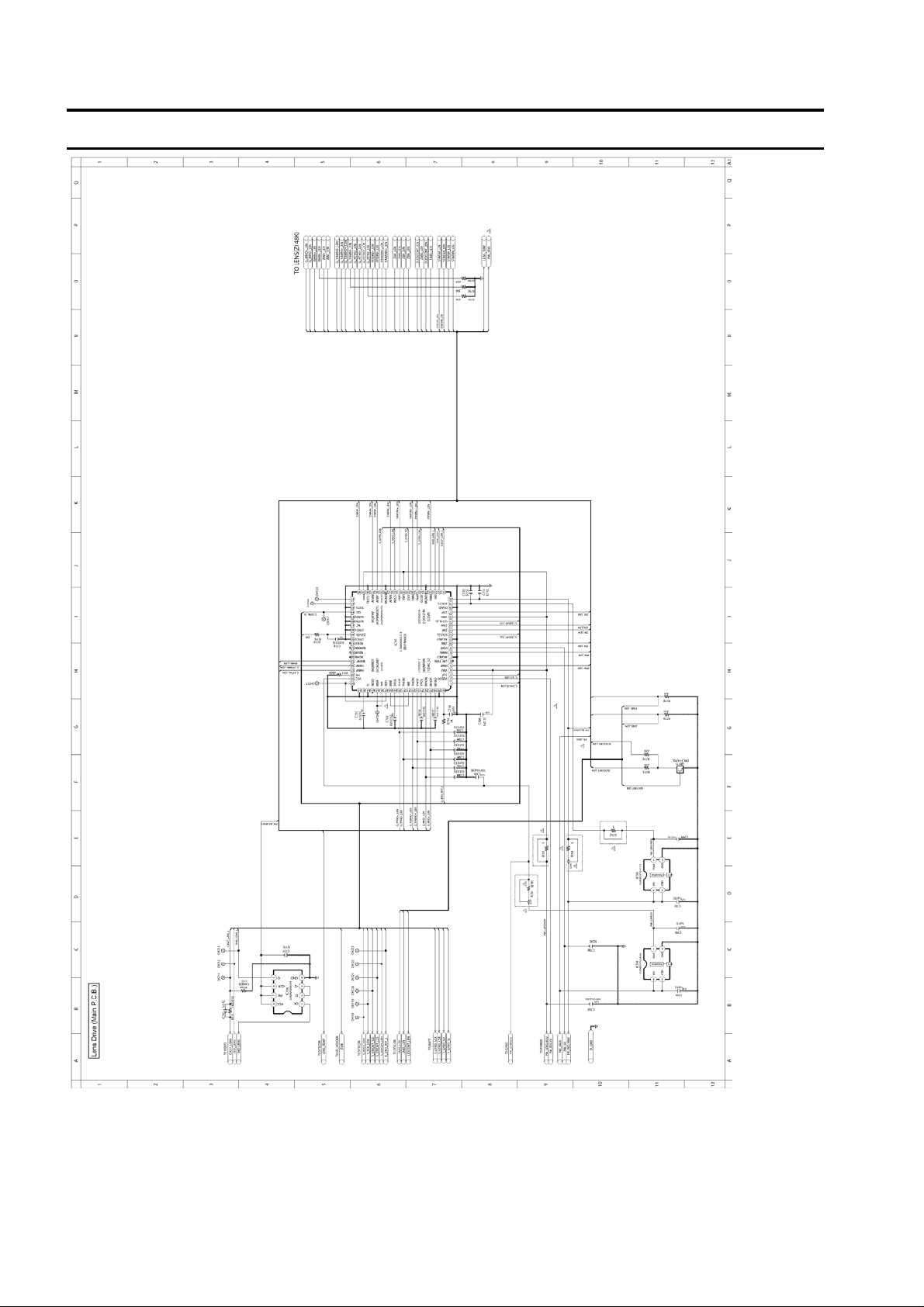
10.5. Lens Drive Circuit Block Diagram
FILTER
MOS
M
5
8
7
21
18
19
20
IC701
(LENS/OIS DRIVE)
6
ZAP
ZBP
IC2006
(SYSTEM CONTROL)
M
IRIS MOTOR
FP6008
ZBN
ZAN
9
HALL
SENSOR
HALL
SENSOR
OIS UNIT
FP6008
PIT DRV+
PIT DRV-
PIT HO+
PIT HIN+
YAW DRV-
YAW DRV+
YAW HIN+
YAW HIN-
YAW HO-
32
33
31
30
29
28
23
22
24
27
26
25
PIT HO-
PIT HIN-
YAW HO+
IRM+
IRM-
FP6008
FP6008
IR HO+
IR HIN+
IR HO-
IR HIN-
HALL
SENSOR
PMP
IRHOP
76
IRHON
31
71
YMP
PHON
28
YMN
70
24
PHOP
57
PHINP
PMN
77
27
IRHINP
55
IRMP
5
IRMN
8
ZAP
14
ZAN
17
ZBN
10
ZBP
13
73
YHON
74
56
YHOP
YHINP
PW GYRO3V
GCSB
GSCK
GSI
GSO
29
23
32
3
12
HD
NSCS
SCK
SDI(V2L)
SDO(L2V)
DAC LD
NPORI
S LENS CS
S LENS CLK
S LENS OUT
22
VD
10
E19
D13
A14
CH711
CH712
CH2012
CH713
CH718
CH719
CH720
15
1
80
S LENS IN
S LENS EVRLD
S LENS RST L
C14
E17
E18
CH721
CH722
CH723
(GYRO SENSOR)
11
MOSI
44
10
MISO
26
8
CSB
CL6401
CL6406
CL6402
CL6403
35
9
SCLK
CL6404
1
VCC
7
VDD
IC6401
ZOOM ENC
ZENC
FENC
MCLKO
FP6008
4
17
3
16
1
FLEDCONT
FABS
LENS TEMP
ZABS
QR775
ZLEDCONT
D20
N4
N1
LENS TEMP
C8
LED CONT
ZOOM MOTOR
FOCUS ENC
HC-V100M/V100 LENS DRIVE CIRCUIT BLOCK DIAGRAM
21
CK27M
M
FOCUS MOTOR
FAP
FAN
FBN
FBP
14
12
11
13
FP6008
AFAN
40
AFAP
37
AFBN
33
AFBP
36
PW REG1.8V
(D-TYPE FLIP FLOP)
4
GND
3
Q
1
CK
2
D
5
Q
6
CLR
8
VCC
7
PR
IC705
IC3401
(ASIC)
C19
GPIOF31
B10
GPIOF32
B19
XVD LENS
W16
CLK27 LENS L
XHD LENS L
XVD LENS
S NSCS LEN
S SCK LEN
S LENDAT S2L
S LENDAT L2S
S DACLD LEN
E LENS RST L
S GYRO CSB
S GYRO SCK
S GYRO SI
S GYRO SO
XHD LENS
13
OUTMODE
LENS DRIVE CIRCUIT BLOCK DIAGRAM
ZOOM
FOCUS
31

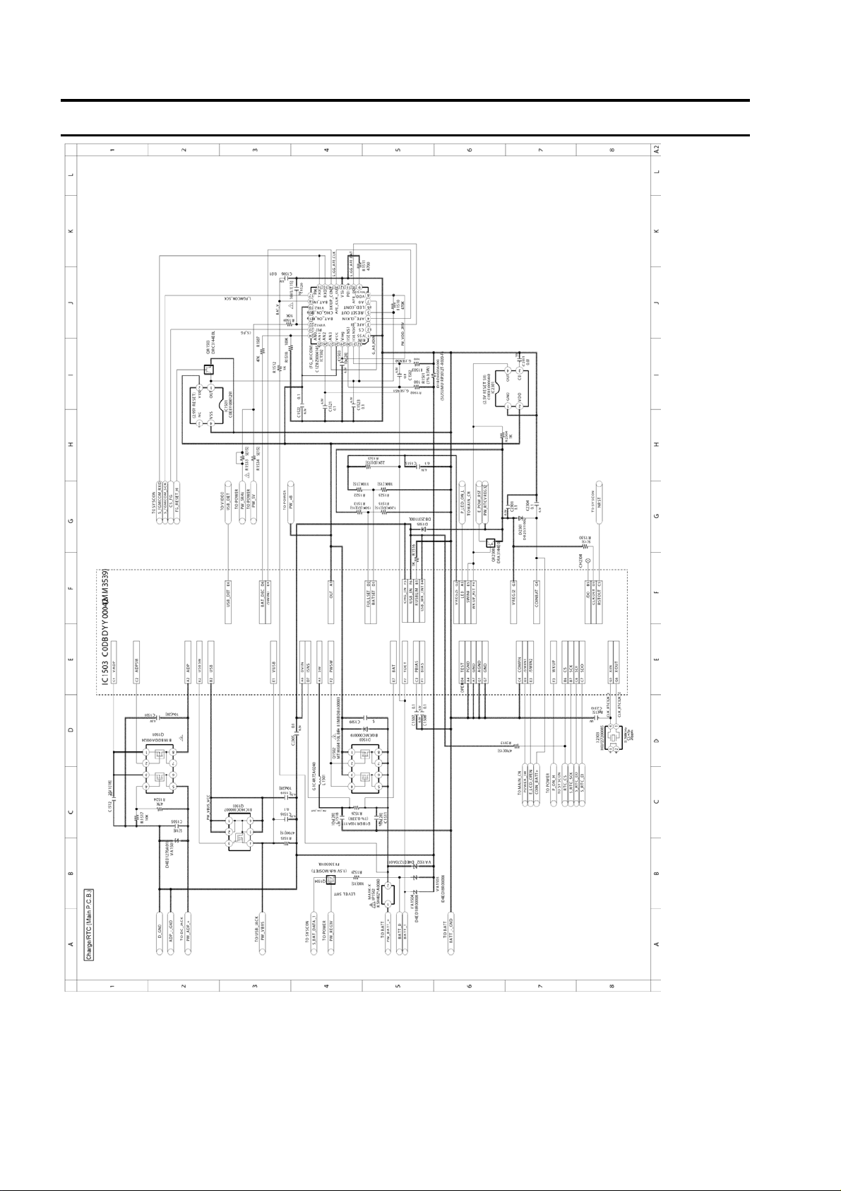
10.6. Power Supply Circuit Block Diagram
POWER SUPPLY CIRCUIT BLOCK DIAGRAM
CL1461
DCG
LX7
RT
FLT7
INV6
VREF5
INV4
VCC
INV7
PGND4
STB6
HS6L
HX567
LED
VO2S
LX1
PGND13
LX3
VO2
LX22
HX13
SELDRV
SCP
LX21
PGND2
INV1
STB5
HX4
UDSEL
VO7
VREGA
HX2
LX4
PWM7
STB1234
INV3
LX5
INV5
GND
PGND567
LX6
22 21 1820 1719 16 15 14 13 12
23
24
25
26
27
28
29
30
31
32
33
11
10
9
8
7
6
5
4
3
2
1
37 38 39 40 4134 35 36
IC1001
(POWER)
JK6701
1
3
4
2
+
T
D
-
JK6401
1
3
2
+
-
HC-V100M/V100 POWER SUPPLY CIRCUIT BLOCK DIAGRAM
BATTERY
DC IN
PW SPK3.2V
PW LENS3.2V
PW 3.2V
PW REG3V
CL1331
CL1441
PW 5V
PW HDM5V
PW RTCVREG32
CL1011
CL1421
CL1321
FUSE RESISTOR:
PW SD3.2V
QR1002
QR1001
QR1101
CL1351
CL1371
CL1471
5
1
4
3
2
IC1471
(REGULATOR)
GND
VOUT
VIN
NCCONT
.
VOUT
NP
VIN
VCONT
5
1
4
3
2
IC1011
(REGULATOR)
GND
Q1501
1
2 3 4
5
6
8
7
IC1502
(BATTERY
MONITOR)
32
1
2
3
4
5
6
7
8
24
23
22
21
313029
9 10 11 12
VSS
CS
AFE DI
AFE CLKIN
/RESET
OUT
LED CONT
A0
VDD
AN0
P07
VIN12
BAT ON H
RIN
ISENS0
ISENS1
VREG
VNVSS
AFE DO
P01
VSS
20
19
18
17
CHG ON H
VIN2
BA
T IN
P06
13 14 15 16
AFE CLK OUT
BKUP CONT
RXD
TXD
28 27 26 25
VCC
AN3
AN2
AN1
Q1502
1
2 3 4
5
6
8
7
1 2 3
46
5
Q1503
IC2006
(SYSTEM CONTROL)
CHA DI
CHA DO
CHA SCK
CHA CS
SW NOREG
S FGMICOM RXD
S FGMICOM TXD
S FGMICOM SCK
CS FG
D15
A16
B15
B16
Y4
V5
W5
U10
C4
A17
IC1501
(VOLTAGE DET.)
4
1
3
2
OUT
VSS
VDD
NC
QR1503
R1261
IC2301
(RESET)
1
2
4
3
VDD
GNDCDOUT
QR2308
CL1105
CL1101
CL1103
Q1504
PW REG3V
BATT RXD
C16
BATT TXD
W6
FG RESET H
IC1503
(RTC/CHARGE/POWER CONTROL)
/SWIN3
VREG32
D6
E4
WKUP
F3
B2
USB
A1
OUT
C2
A3
USBSW
BA
T DEC
G2
VREG25
(R1261/R6409)
Please check the Fuse Resistor when an output
voltage does not output.
IP1502
IP6401
1
USB TERMINAL
VBUS
JK6402
IC1441
(REGULATOR)
3
2
4
1
VIN
VOUT
STBY
GND
PW PLL1.1V
PW LENS1.5V
PW EV6X 1.1V
PW 5.4V
PW REG1.8V
PW SENS1.8V
PW DDR1.5V
CH1231
CH1422
CH2014
CH1101
ADPSW
PWSW
A2
ADP
C1
VADP
SW
F2
USB DET
E6
E2
E7
BAT
E1
VUSB
D7
ISNS
F7
TDET
C5
RSTOUT
L2
NRST
B6
CS
B7
SCK
E5
SWIN4
F4
WKUP RST
CL1341
IC703
(REGULATOR)
3
2
4
1
VIN
VOUT
STBY
GND
D902-905
(LCD BACK LIGHT)
C6
SDI
C7
SDO
S6401
POWER ON/OFF
LI BATT
D3
/SWIN1
B6401
G4
COINBAT
G3
DVIN
A6
CHG EN
F5
FULLSET
D2
BATSET
D1
USB EN
F6
USB WK CNT
B4
CL1001
CL1002
R6409
QR2002
IC704
(REGULATOR)
3
2
4
1
VIN
VOUT
STBY
GND
PW LENS3V
IC1421
(REGULATOR)
3
2
4
1
VIN
VOUT
CE
GND
5
1
4
3
2
IC301
(REGULATOR)
GND
OUT
IN
NCCE
PW MOS2.7V
PW LCD3V
LCD ON H
(From IC2006-J19)
Q1421
Q1422
PW 5V
QR3406
QR3405
BL CONT
(From IC3401-E5)
VBUS
(To IC3401-L24)
U15
MOSSENS ONH
32
11 Wiring Connection Diagram
HC-V100M/V100 INTERCONNECTION DIAGRAM
INTERCONNECTION DIAGRAM
MAIN P.C.B.
(FOIL SIDE)
:
(COMPONENT SIDE)
ESD P.C.B.
(FOIL SIDE)
P6003
65432
1
BATT
-
BATT
-
D
T
BATT +
BATT +
LENS TEMP
ZABS
IRHIN
-
IRHIN+
IRM+
FBN
FBP
FENCVCC
FLEDCONT
ZAP
ZAN
YAWDRV
-
YAWHO
-
YAWHO+
PITHO
-
PITHO+
PITDRV
-
246
8
1012141618202224262830
32
ZENC VCC
ZLEDCONT
IRHO
-
IRHO+
IRM
-
FAN
FAP
FABS
ZBN
ZBP
YAWDRV+
YAWHIN
-
YAWHIN+
PITHIN
-
PITHIN+
PITDRV+
13579
11
1315171921232527293133
FP6008
PP301
1
2
3
4
5
6
7
8
9
10
11
12
13
14
15
16
17
18
19
20
NC
NC
NC
RSTN
SDI
HD
SCK
SCS
VD
MCLK
2.7V
DOBP
DOBM
DCKP
DCKM
DOAP
DOAM
1.8V
1.8V
1.8V
MONITOR FPC
FP6001
123456789
10
DAT3
DAT0
DAT1
DAT2
CMD
GND
CLK
GND
VDD
VDD
FP3201
10
987654321
DAT3
DAT0
DAT1
DAT2
CMD
GND
CLK
GND
VDD
VDD
P6701
1
2
3
4
5
6
BATT +
BATT +
T
D
BATT
-
BATT
-
JK6701
123
4
+
T
D
-
BATTERY
BATTERY CATCHER P.C.B.
(FOIL SIDE)
:
(COMPONENT SIDE)
MOS UNIT
LENS UNIT
SD HOLDER P.C.B.
(FOIL SIDE)
PP6001
NOREG
NOREG
NOREG
NOREG
NOREG
NOREG
NOREG
SP OUT1
SP OUT2
PW SD3R2V
PW SD3R2V
PW SD3R2V
E CARD DET
ZOOMAD
PHOPO2 ZENOSHI
STANDBY LED
POWER LED
VTR KEY 1
D GND
PW LIBATT
E CARD PRO
PW REG3V
CARD LED B
E KEYIN4
POWER SW
SD CMD
D GND
SD DATA2
SD DATA3
SD DATA0
SD DATA1
D GND
SD CLK
D GND
D GND
D GND
S GYRO CSB
S GYRO SCK
S GYRO SO
S GYRO SI
PW GYRO3V
GYRO GND
GYRO GND
VBUS
VBUS
ID
D GND
D
-
D+
D GND
25
24
23
22
21
20
19
18
17
16
15
14
13
12
11
10
9
8
7
6
5
4
3
2
1
26
27
28
29
30
31
32
33
34
35
36
37
38
39
40
41
42
43
44
45
46
47
48
49
50
PS6401
25242322212019181716151413
121110
987654321
26272829303132333435363738394041424344454647484950
FP6402
10
987654321
NC
GND
ZOOMAD
AVREF
PHOTO2 ZENOSHI
STANDBY LED
POWER LED
GND
AVREF
VTR KEY 1
SP OUT1
SP OUT2
1
2
P6401
SPEAKER
FP6003
65432
1
ECM R
ECM R
D GND
D GND
ECM L
ECM L
MIC
NC
NC
LCD RVS
PW LCDBL L
PW LCDBL H
D GND
D GND
RST
S CS LCD
PW REG3V
BUS9 LCDYC7
BUS9 LCDYC5
BUS9 LCDYC3
BUS9 LCDYC1
D GND
D GND
BUS9 LCD V
PW REG1R8V
NC
NC
KEYIN6
PW LCDBL L
PW LCDBL H
D GND
D GND
S CLK LCD
S DO LCD
PW REG3V
BUS9 LCDYC6
BUS9 LCDYC4
BUS9 LCDYC2
BUS9 LCDYC0
CLK18 LCD
BUS9 LCD H
PW REG1R8V
FP6004
MONITOR P.C.B.
(FOIL SIDE)
1
2
3
4
5
6
7
8
9
10
11
12
13
14
15
16
17
18
19
20
21
22
23
24
25
26
27
28
29
30
FP901
FP904
GND
C3P
C4P
VGL
C1P
C2P
VSS2
VCI
CXN
VCOMH
VGM
VSS1
VDDL
HSYNC
NC
DB1
DB3
DB5
DB7
SCL
RESET
2
4
6
8
10
12
14
16
18
20
22
24
26
28
30
32
34
36
38
40
VGH
C3N
C4N
VS
C1N
C2N
VCIX2
CXP
VCIM
VCOML
VCOM
VDDIO
VSYNC
DCLK
DB0
DB2
DB4
DB6
SDA
SCS
1
3
5
7
9
11
13
15
17
19
21
23
25
27
29
31
33
35
37
39
41
LCD UNIT
TOP OPERATION
246
8
10121416182022242628303234
13579
11
1315171921232527293133
35
PW REG3V/1R8V
BUS9 LCD V
BUS9 LCD H
D GND
CLK18 LCD
D GND
BUS9 LCDYC0
BUS9 LCDYC1
BUS9 LCDYC2
BUS9 LCDYC3
BUS9 LCDYC4
BUS9 LCDYC5
BUS9 LCDYC6
BUS9 LCDYC7
PW REG3V
S DO LCD
S CS LCD
S CLK LCD
CHIMEI RST
D GND
D GND
D GND
PW LCDBL H
PW LCDBL L
OP/COIN BATT+
LCD RVS
S AD TPX TOP
S AD TPYLEFT
S AD TPX BOT
S AD TPYRIGHT
NOREG
NOREG
NOREG
NOREG
NOREG
NOREG
NOREG
SP OUT1
SP OUT2
PW SD3R2V
PW SD3R2V
PW SD3R2V
E CARD DET
ZOOMAD
PHOPO2 ZENOSHI
STANDBY LED
POWER LED
VTR KEY 1
D GND
PW LIBATT
E CARD PRO
PW REG3V
CARD LED B
E KEYIN4
POWER SW
SD CMD
D GND
SD DATA2
SD DATA3
SD DATA0
SD DATA1
D GND
SD CLK
D GND
D GND
D GND
S GYRO CSB
S GYRO SCK
S GYRO SO
S GYRO SI
PW GYRO3V
GYRO GND
GYRO GND
VBUS
VBUS
ID
D GND
D
D+
D GND
PW REG3V
KEYIN6
D GND
D GND
4
3
2
1
FP503
LCD OP FPC
ECM FPC
HC-V100M only
11.1. Interconnection Diagram
33
Model No. : HC-V100/V100M Schematic Diagram Note

Model No. : HC-V100/V100M Parts List Note
Model No. : HC-V100/V100M Main Connection (Main P.C.B.)

Model No. : HC-V100/V100M Video (Main P.C.B.)

Model No. : HC-V100/V100M HD Video (Main P.C.B.)
Model No. : HC-V100/V100M Lens Drive (Main P.C.B.)

Model No. : HC-V100/V100M Syscon (Main P.C.B.)
Model No. : HC-V100/V100M Charge/RTC (Main P.C.B.)

Model No. : HC-V100/V100M MIC (Main P.C.B.)

Model No. : HC-V100/V100M Power (Main P.C.B.)

Model No. : HC-V100/V100M MOS Connection (Main P.C.B.)

Model No. : HC-V100/V100M SD Holder (SD Holder P.C.B.)

Model No. : HC-V100/V100M Main P.C.B. (Component Side)

Model No. : HC-V100/V100M Main P.C.B. (Foil Side)
Model No. : HC-V100/V100M SD Holder P.C.B.(Component Side)

Model No. : HC-V100/V100M SD Holder P.C.B.(Foil Side)

Model No. : HC-V100/V100M Parts List
Safety
Ref.
No.
B6401 ML-614S/DN BUTTON BATTERY 1 [ENERGY]
C302 F1L0J1040001 C.CAPACITOR CH 6.3V 0.1U 1
C303 F1G0J1050007 C.CAPACITOR CH 6.3V 1U 1
C304 F1G0J1050007 C.CAPACITOR CH 6.3V 1U 1
C305 F1G1C104A077 C.CAPACITO R CH 16V 0.1U 1
C309 F1G0J1050007 C.CAPACITOR CH 6.3V 1U 1
C701 F1G0J1050007 C.CAPACITOR CH 6.3V 1U 1
C702 F1G0J1050007 C.CAPACITOR CH 6.3V 1U 1
C703 F1J0J106A049 C.CAPACITOR CH 6.3V 10U 1
C704 F1G0J1050007 C.CAPACITOR CH 6.3V 1U 1
C705 F1G0J1050007 C.CAPACITOR CH 6.3V 1U 1
C706 F1G0J1050007 C.CAPACITOR CH 6.3V 1U 1
C709 F1J0J106A049 C.CAPACITOR CH 6.3V 10U 1
C715 F1G1C104A077 C.CAPACITO R CH 16V 0.1U 1
C716 F1L1A103A016 C.CAPACITO R CH 10V 0.01U 1
C718 F1G1E1030005 C.CAPACITO R CH 25V 0.01U 1
C719 F1G1E1030005 C.CAPACITO R CH 25V 0.01U 1
C720 F1G1E1030005 C.CAPACITO R CH 25V 0.01U 1
C721 F1G1E1030005 C.CAPACITO R CH 25V 0.01U 1
C722 F1G1E1030005 C.CAPACITO R CH 25V 0.01U 1
C723 F1G1E1030005 C.CAPACITO R CH 25V 0.01U 1
C724 F1G1E1030005 C.CAPACITO R CH 25V 0.01U 1
C725 F1G1E1030005 C.CAPACITO R CH 25V 0.01U 1
C726 F1G1E1030005 C.CAPACITO R CH 25V 0.01U 1
C727 F1G1E1030005 C.CAPACITO R CH 25V 0.01U 1
C1001 F1J0J106A049 C.CAPACITOR CH 6.3V 10U 1
C1012 F1G1H102A640 C.CAPACITOR CH 50V 1000P 1
C1013 F1G0J1050007 C.CAPACITOR CH 6.3V 1U 1
C1061 F1H0J4750004 C.CAPACITOR CH 6.3V 4.7U 1
C1101 F1G0J1050007 C.CAPACITOR CH 6.3V 1U 1
C1102 F1G1C104A077 C.CAPACITOR CH 16V 0.1U 1
C1103 F1G0J1050007 C.CAPACITOR CH 6.3V 1U 1
C1161 F1G0J1050007 C.CAPACITOR CH 6.3V 1U 1
C1221 F1G0J1050007 C.CAPACITOR CH 6.3V 1U 1
C1222 F1J0J106A049 C.CAPACITOR CH 6.3V 10U 1
C1231 F1G0J1050007 C.CAPACITOR CH 6.3V 1U 1
C1232 F1J0J106A049 C.CAPACITOR CH 6.3V 10U 1
C1242 F1J0J106A049 C.CAPACITOR CH 6.3V 10U 1
C1251 F1G0J1050007 C.CAPACITOR CH 6.3V 1U 1
C1252 F1J0J106A049 C.CAPACITOR CH 6.3V 10U 1
C1261 F1H1E105A116 C.CAPACITOR CH 25V 1U 1
C1271 F1G0J1050007 C.CAPACITOR CH 6.3V 1U 1
C1272 F1J0J106A049 C.CAPACITOR CH 6.3V 10U 1
C1273 F1G1H220A644 C.CAPACITOR CH 50V 22P 1
C1342 F3F0G476A030 E.CAPACITOR CH 4V 47U 1
C1352 F3F0G476A030 E.CAPACITOR CH 4V 47U 1
C1422 F1G0J1050007 C.CAPACITOR CH 6.3V 1U 1
C1423 F1G0J1050007 C.CAPACITOR CH 6.3V 1U 1
C1441 F1H0J4750004 C.CAPACITOR CH 6.3V 4.7U 1
C1471 F1G0J1050007 C.CAPACITOR CH 6.3V 1U 1
C1501 F1J0J106A049 C.CAPACITOR CH 6.3V 10U 1
C1502 F1L0J1040001 C.CAPACITOR CH 6.3V 0.1U 1
C1503 F1J0J106A049 C.CAPACITOR CH 6.3V 10U 1
C1506 F1L1A103A016 C.CAPACITOR CH 10V 0.01U 1
C1507 F1L0J1040001 C.CAPACITOR CH 6.3V 0.1U 1
C1508 F1L0J1040001 C.CAPACITOR CH 6.3V 0.1U 1
C1511 F1J0J106A049 C.CAPACITOR CH 6.3V 10U 1
C1512 F1H1E105A116 C.CAPACITOR CH 25V 1U 1
C1515 F1L0J1040001 C.CAPACITOR CH 6.3V 0.1U 1
C1516 F1L0J1040001 C.CAPACITOR CH 6.3V 0.1U 1
C1518 F1J0J106A049 C.CAPACITOR CH 6.3V 10U 1
C1519 F1J0J106A049 C.CAPACITOR CH 6.3V 10U 1
Part No. Part Name & Description Q'ty Remarks

Model No. : HC-V100/V100M Parts List
Safety
Ref.
No.
C1520 F1G1C104A077 C.CAPACITOR CH 16V 0.1U 1
C1521 F1L0J1040001 C.CAPACITOR CH 6.3V 0.1U 1
C1522 F1L0J1040001 C.CAPACITOR CH 6.3V 0.1U 1
C1523 F1L0J1040001 C.CAPACITOR CH 6.3V 0.1U 1
C2002 F3F0J226A032 T.CAPACITOR CH 6.3V 22U 1
C2003 F1G1C104A077 C.CAPACITOR CH 16V 0.1U 1
C2004 F1G0J1050007 C.CAPACITOR CH 6.3V 1U 1
C2005 F1G1E1030005 C.CAPACITOR CH 25V 0.01U 1
C2006 F1G1E1030005 C.CAPACITOR CH 25V 0.01U 1
C2008 F1G0J1050007 C.CAPACITOR CH 6.3V 1U 1
C2011 F1L1A103A016 C.CAPACITOR CH 10V 0.01U 1
C2014 F1L1A103A016 C.CAPACITOR CH 10V 0.01U 1
C2017 F1L1A103A016 C.CAPACITOR CH 10V 0.01U 1
C2020 F1L1A103A016 C.CAPACITOR CH 10V 0.01U 1
C2021 F1L1A103A016 C.CAPACITOR CH 10V 0.01U 1
C2022 F1L1A103A016 C.CAPACITOR CH 10V 0.01U 1
C2301 F1L0J1040001 C.CAPACITOR CH 6.3V 0.1U 1
C2304 F1L0J1040001 C.CAPACITOR CH 6.3V 0.1U 1
C2305 F1L0J1040001 C.CAPACITOR CH 6.3V 0.1U 1
C2310 F1G1H8R0A642 CAPACITOR 1
C2311 F1L1A103A016 C.CAPACITOR CH 10V 0.01U 1
C3401 F3G0J107A017 C.CAPACITOR CH 6.3V 100U 1
C3402 F1H0J4750004 C.CAPACITOR CH 6.3V 4.7U 1
C3403 F1G0J1050007 C.CAPACITOR CH 6.3V 1U 1
C3404 F1G0J1050007 C.CAPACITOR CH 6.3V 1U 1
C3405 F1L0J1040001 C.CAPACITOR CH 6.3V 0.1U 1
C3406 F1G0J1050007 C.CAPACITOR CH 6.3V 1U 1
C3407 F1G0J1050007 C.CAPACITOR CH 6.3V 1U 1
C3408 F1G0J1050007 C.CAPACITOR CH 6.3V 1U 1
C3409 F1J0J106A049 C.CAPACITOR CH 6.3V 10U 1
C3410 F1J0J106A049 C.CAPACITOR CH 6.3V 10U 1
C3411 F3F0J226A032 T.CAPACITOR CH 6.3V 22U 1
C3412 F1J0J106A049 C.CAPACITOR CH 6.3V 10U 1
C3413 F1L0J1040001 C.CAPACITOR CH 6.3V 0.1U 1
C3414 F1G0J1050007 C.CAPACITOR CH 6.3V 1U 1
C3416 F1L0J1040001 C.CAPACITOR CH 6.3V 0.1U 1
C3417 F1L0J1040001 C.CAPACITOR CH 6.3V 0.1U 1
C3418 F1L0J1040001 C.CAPACITOR CH 6.3V 0.1U 1
C3419 F1L0J1040001 C.CAPACITOR CH 6.3V 0.1U 1
C3420 F1L0J1040001 C.CAPACITOR CH 6.3V 0.1U 1
C3421 F1L0J1040001 C.CAPACITOR CH 6.3V 0.1U 1
C3422 F1L0J1040001 C.CAPACITOR CH 6.3V 0.1U 1
C3424 F1L0J1040001 C.CAPACITOR CH 6.3V 0.1U 1
C3425 F1L0J1040001 C.CAPACITOR CH 6.3V 0.1U 1
C3426 F1L0J1040001 C.CAPACITOR CH 6.3V 0.1U 1
C3427 F1L0J1040001 C.CAPACITOR CH 6.3V 0.1U 1
C3429 F1L0J1040001 C.CAPACITOR CH 6.3V 0.1U 1
C3430 F1L0J1040001 C.CAPACITOR CH 6.3V 0.1U 1
C3431 F1G1H120A644 C.CAPACITOR CH 50V 12P 1
C3432 F1G1H8R0A642 CAPACITOR 1
C3433 F1G0J1050007 C.CAPACITOR CH 6.3V 1U 1
C3434 F1G0J1050007 C.CAPACITOR CH 6.3V 1U 1
C3435 F1J0J106A049 C.CAPACITOR CH 6.3V 10U 1
C3437 F1J0J106A049 C.CAPACITOR CH 6.3V 10U 1
C3438 F1J0J106A049 C.CAPACITOR CH 6.3V 10U 1
C3439 F1G1C104A077 C.CAPACITOR CH 16V 0.1U 1
C3440 F1G1C104A077 C.CAPACITOR CH 16V 0.1U 1
C3441 F1G1H182A640 C.CAPACITOR CH 50V 1800P 1
C3442 F1L0J1040001 C.CAPACITOR CH 6.3V 0.1U 1
C3443 F1L0J1040001 C.CAPACITOR CH 6.3V 0.1U 1
C3444 F1L1A103A016 C.CAPACITOR CH 10V 0.01U 1
C3445 F1L1A103A016 C.CAPACITOR CH 10V 0.01U 1
Part No. Part Name & Description Q'ty Remarks

Model No. : HC-V100/V100M Parts List
Safety
Ref.
No.
C3446 F1L0J1040001 C.CAPACITOR CH 6.3V 0.1U 1
C3447 F1L0J1040001 C.CAPACITOR CH 6.3V 0.1U 1
C3448 F1L0J1040001 C.CAPACITOR CH 6.3V 0.1U 1
C3453 F1L0J1040001 C.CAPACITOR CH 6.3V 0.1U 1
C3455 F1J0J106A049 C.CAPACITOR CH 6.3V 10U 1
C3456 F1L0J1040001 C.CAPACITOR CH 6.3V 0.1U 1
C3457 F1L0J1040001 C.CAPACITOR CH 6.3V 0.1U 1
C3458 F1L0J1040001 C.CAPACITOR CH 6.3V 0.1U 1
C3459 F1L0J1040001 C.CAPACITOR CH 6.3V 0.1U 1
C3464 F1J0J106A049 C.CAPACITOR CH 6.3V 10U 1
C3465 F1L0J1040001 C.CAPACITOR CH 6.3V 0.1U 1
C3466 F1L0J1040001 C.CAPACITOR CH 6.3V 0.1U 1
C3467 F1L0J1040001 C.CAPACITOR CH 6.3V 0.1U 1
C3471 F1L0J1040001 C.CAPACITOR CH 6.3V 0.1U 1
C3472 F1G1C104A077 C.CAPACITOR CH 16V 0.1U 1
C3473 F3G0J107A017 C.CAPACITOR CH 6.3V 100U 1
C3605 F1J0J106A049 C.CAPACITOR CH 6.3V 10U 1
C3701 F1G0J1050007 C.CAPACITOR CH 6.3V 1U 1
C3702 F1G0J1050007 C.CAPACITOR CH 6.3V 1U 1
C3703 F1G0J1050007 C.CAPACITOR CH 6.3V 1U 1
C3704 F1H0J4750004 C.CAPACITOR CH 6.3V 4.7U 1
C3705 F1H0J4750004 C.CAPACITOR CH 6.3V 4.7U 1
C3706 F1H0J4750004 C.CAPACITOR CH 6.3V 4.7U 1
C3707 F1J0J106A049 C.CAPACITOR CH 6.3V 10U 1
C3751 F1J0J106A049 C.CAPACITOR CH 6.3V 10U 1
C3752 F1L0J1040001 C.CAPACITOR CH 6.3V 0.1U 1
C3753 F1J0J106A049 C.CAPACITOR CH 6.3V 10U 1
C3754 F1J0J106A049 C.CAPACITOR CH 6.3V 10U 1
C3755 F1L0J1040001 C.CAPACITOR CH 6.3V 0.1U 1
C3756 F1L1A103A016 C.CAPACITOR CH 10V 0.01U 1
C3757 F1G1H220A644 C.CAPACITOR CH 50V 22P 1
C3758 F1L0J1040001 C.CAPACITOR CH 6.3V 0.1U 1
C3759 F1G1H472A571 C.CAPACITOR CH 50V 4700P 1
C3760 F1L0J1040001 C.CAPACITOR CH 6.3V 0.1U 1
C3761 F1L0J1040001 C.CAPACITOR CH 6.3V 0.1U 1
C3762 F1L0J1040001 C.CAPACITOR CH 6.3V 0.1U 1
C3906 F1G1C104A077 C.CAPACITOR CH 16V 0.1U 1
C3907 F3G0J107A017 C.CAPACITOR CH 6.3V 100U 1
C3908 F1G1E1030005 C.CAPACITOR CH 25V 0.01U 1
C3909 F1G1C104A077 C.CAPACITOR CH 16V 0.1U 1
C3910 F1G1E1030005 C.CAPACITOR CH 25V 0.01U 1
C3911 F1G0J1050007 C.CAPACITOR CH 6.3V 1U 1
C4801 F1L0J1040001 C.CAPACITOR CH 6.3V 0.1U 1
C4802 F1L0J1040001 C.CAPACITOR CH 6.3V 0.1U 1
C4804 F1J0J106A049 C.CAPACITOR CH 6.3V 10U 1
C6001 F1G1C104A077 C.CAPACITOR CH 16V 0.1U 1
C6002 F1L0J1040001 C.CAPACITOR CH 6.3V 0.1U 1
C6003 F1L0J1040001 C.CAPACITOR CH 6.3V 0.1U 1
C6004 F1G1H220A644 C.CAPACITOR CH 50V 22P 1
C6005 F1G1H472A571 C.CAPACITOR CH 50V 4700P 1
C6006 F1G1H472A571 C.CAPACITOR CH 50V 4700P 1
C6007 ECJ1VB1A105K C.CAPACITOR CH 10V 1U 1
C6008 F1G1H220A644 C.CAPACITOR CH 50V 22P 1
C6009 F1L0J1040001 C.CAPACITOR CH 6.3V 0.1U 1
C6011 F1L0J1040001 C.CAPACITOR CH 6.3V 0.1U 1 MP,MPC,MPU,MGK
C6012 F1G1H220A644 C.CAPACITOR CH 50V 22P 1
C6013 F1G1H220A644 C.CAPACITOR CH 50V 22P 1
C6014 F1G1H220A644 C.CAPACITOR CH 50V 22P 1
C6016 F1G1C104A077 C.CAPACITOR CH 16V 0.1U 1
C6017 F1G1H220A644 C.CAPACITOR CH 50V 22P 1
C6018 F1G1H220A644 C.CAPACITOR CH 50V 22P 1
C6019 F1L0J1040001 C.CAPACITOR CH 6.3V 0.1U 1
Part No. Part Name & Description Q'ty Remarks

Model No. : HC-V100/V100M Parts List
Safety
Ref.
No.
C6020 F1G0J1050007 C.CAPACITOR CH 6.3V 1U 1
C6021 F1G0J1050007 C.CAPACITOR CH 6.3V 1U 1
C6022 F1L0J1040001 C.CAPACITOR CH 6.3V 0.1U 1
C6023 F1G1H220A644 C.CAPACITOR CH 50V 22P 1
C6401 F1J1A106A043 C.CAPACITOR CH 10V 10U 1
C6403 F1G1C104A077 C.CAPACITOR CH 16V 0.1U 1
C6404 F1G1C104A077 C.CAPACITOR CH 16V 0.1U 1
C6405 F1G1C104A077 C.CAPACITOR CH 16V 0.1U 1
C6407 F1G1C104A077 C.CAPACITOR CH 16V 0.1U 1
C6408 ECJ1VB1A105K C.CAPACITOR CH 10V 1U 1
C6412 F1H1E105A116 C.CAPACITOR CH 25V 1U 1
D1261 B0JCMD000077 DIODE 1 E.S.D.
D1271 B0JCGD000016 DIODE 1 E.S.D.
D1503 B0JCMC000019 DIODE 1 E.S.D.
D1505 DB2S31100L DIODE 1 E.S.D.
D2301 DB2S31100L DIODE 1 E.S.D.
D3401 DB2S31100L DIODE 1 E.S.D.
D6451 B3AAB0000343 LED 1 E.S.D.
FL6002 J0ZZB0000148 FILTER 1
FL6003 J0ZZB0000148 FILTER 1
FL6004 F1H0J105A037 C.CAPACITOR CH 6.3V 1U 1
FP6001 K1MY10BA0370 CONNECTOR 10P 1 MP,MPC,MPU,MGK
FP6004 K1MY35AA0199 CONNECTOR 35P 1
FP6008 K1MY33AA0199 CONNECTOR 33P 1
FP6402 K1MY10BA0370 CONNECTOR 10P 1
HS3901 K1NA09E00098 SD CARD CONNECTOR 1
IC301 C0DBGYY02227 IC 1 E.S.D.
IC701 C1AB00003719 IC 1 E.S.D.
IC703 C0DBGYY01172 IC 1 E.S.D.
IC704 C0DBGYY02595 IC 1 E.S.D.
IC705 C0JBAF000544 IC 1 E.S.D.
IC1001 C1ZBZ0004347 IC 1 E.S.D.
IC1011 C0CBCDC00073 IC 1 E.S.D.
IC1421 C0CBCYY00078 IC 1 E.S.D.
IC1441 C0DBGYY00534 IC 1 E.S.D.
IC1471 C0DBGHD00008 IC 1 E.S.D.
IC1501 C0EBY0001291 IC 1 E.S.D.
IC1502 C1ZBZ0004145 IC 1 E.S.D.
IC1503 C0DBDYY00042 IC 1 E.S.D.
IC2002 C3EBJC000100 IC 1 E.S.D.
IC2006 MN103SK7NCD IC 1 E.S.D.
IC2301 C0EBE0000442 IC 1 E.S.D.
IC3401 C1AB00003857 IC 1 E.S.D.
IC3402 C3ABTY000059 IC 1 E.S.D.
IC3403 C3ABTY000059 IC 1 E.S.D.
IC3404 TC58NVM9F12A IC 1 E.S.D.
IC3701 C9ZB00000575 IC 1 E.S.D.
IC3751 C1AB00002890 IC 1 E.S.D.
IC6401 EWTS9PSL1A IC 1 E.S.D.
IP1502 K5H402YA0080 FUSE 1
IP6401 K5H402YA0080 FUSE 1
JK6002 K2HZ112E0001 JACK, AV MULTI 1
JK6003 K1FA119E0020 JACK, HDMI 1
JK6401 K2EBYB000003 JACK, DC 1
JK6402 K2HZ105E0011 JACK, USB 1
L301 G1C100KA0115 CHIP INDUCTOR 10UH 1
L302 G1C100KA0115 CHIP INDUCTOR 10UH 1
L1221 G1C3R3MA0249 CHIP INDUCTOR 3.3UH 1
L1231 G1C100MA0249 CHIP INDUCTOR 10UH 1
L1241 G1C3R3MA0249 CHIP INDUCTOR 3.3UH 1
L1251 G1C100MA0426 CHIP INDUCTOR 10UH 1
L1261 G1C6R8MA0061 CHIP INDUCTOR 6.8UH 1
Part No. Part Name & Description Q'ty Remarks

Model No. : HC-V100/V100M Parts List
Safety
Ref.
No.
L1271 G1C6R8MA0478 CHIP INDUCTOR 6.8UH 1
L1501 G1C4R7ZA0240 CHIP INDUCTOR 4.7UH 1
L3402 G1C100MA0495 CHIP INDUCTOR 10UH 1
L3403 G1C100MA0495 CHIP INDUCTOR 10UH 1
L3404 G1C100MA0408 CHIP INDUCTOR 10UH 1
L3603 G1C100KA0115 CHIP INDUCTOR 10UH 1
L3701 G1C100KA0115 CHIP INDUCTOR 10UH 1
L3702 G1C100KA0115 CHIP INDUCTOR 10UH 1
L3751 G1C100KA0115 CHIP INDUCTOR 10UH 1
L3752 G1C100KA0115 CHIP INDUCTOR 10UH 1
L3753 G1C100KA0115 CHIP INDUCTOR 10UH 1
LB301 J0JBC0000099 FILTER 1
LB3401 J0JBC0000099 FILTER 1
LB3402 J0JBC0000099 FILTER 1 MP,MPC,MPU,MGK
LB6001 J0JCC0000276 FILTER 1
LB6002 J0JCC0000276 FILTER 1
LB6003 J0JCC0000276 FILTER 1
LB6004 J0JCC0000276 FILTER 1
LB6005 J0JCC0000408 FILTER 1
LB6006 J0JCC0000276 FILTER 1
LB6007 J0JCC0000408 FILTER 1
LB6008 J0JCC0000276 FILTER 1
LB6009 J0JCC0000276 FILTER 1
LB6010 J0JCC0000408 FILTER 1
LB6011 J0JGC0000059 FILTER 1 MP,MPC,MPU,MGK
LB6012 J0JBC0000115 FILTER 1
LB6401 J0JJC0000015 FILTER 1
LB6402 J0JJC0000015 FILTER 1
P6401 K1KA02BA0014 CONNECTOR 2P 1
PP301 K1KY20AA0805 CONNECTOR 20P 1
PP6001 K1KY50BA0095 CONNECTOR 50P 1
PS6401 K1KB50AA0094 CONNECTOR 50P 1
Q1421 B1ADGD000013 TRANSISTOR 1 E.S.D.
Q1422 DSC300100L TRANSISTOR 1 E.S.D.
Q1501 B1MBDDA00024 TRANSISTOR 1 E.S.D.
Q1502 MTM684110LBF TRANSISTOR 1 E.S.D.
Q1503 B1CHQC000007 TRANSISTOR 1 E.S.D.
Q1504 FK3303010L TRANSISTOR 1 E.S.D.
Q2001 DSA300100L TRANSISTOR 1 E.S.D.
Q3901 B1ADKB000015 TRANSISTOR 1 E.S.D.
Q4801 DSC300100L TRANSISTOR 1 E.S.D.
Q4802 DSC300100L TRANSISTOR 1 E.S.D.
Q4803 DSC300100L TRANSISTOR 1 E.S.D.
QR775 DRC3143T0L TRANSISTOR-RESISTOR 1 E.S.D.
QR1001 DRC3143E0L TRANSISTOR-RESISTOR 1 E.S.D.
QR1002 DRA3124X0L TRANSISTOR-RESISTOR 1 E.S.D.
QR1101 DRC3114E0L TRANSISTOR-RESISTOR 1 E.S.D.
QR1503 DRC3144E0L TRANSISTOR-RESISTOR 1 E.S.D.
QR2002 DRC3114T0L TRANSISTOR-RESISTOR 1 E.S.D.
QR2308 DRA3144E0L TRANSISTOR-RESISTOR 1 E.S.D.
QR3405 DRC3144W0L TRANSISTOR-RESISTOR 1 E.S.D.
QR3406 DRA3144E0L TRANSISTOR-RESISTOR 1 E.S.D.
QR6002 DRA3124X0L TRANSISTOR-RESISTOR 1 E.S.D.
QR6003 DRA3114T0L TRANSISTOR-RESISTOR 1 E.S.D.
QR6007 DRA3124X0L TRANSISTOR-RESISTOR 1 E.S.D.
QR6008 DRC3114E0L TRANSISTOR-RESISTOR 1 E.S.D.
QR6402 DRA9114T0L TRANSISTOR-RESISTOR 1 E.S.D.
R302 ERJ1GEJ102 M.RESISTOR CH 1/20W 1K 1
R304 ERJ1GEJ272 M.RESISTOR CH 1/20W 2.7K 1
R305 D0GA470JA023 RESISTOR 1
R716 ERJ1GEJ102 M.RESISTOR CH 1/20W 1K 1
R717 ERJ1GEJ682 M.RESISTOR CH 1/20W 6.8K 1
Part No. Part Name & Description Q'ty Remarks
Model No. : HC-V100/V100M Parts List
Safety
Ref.
No.
R719 D0GAR00J0005 RESISTOR 1
R731 ERJ2RHD102X M.RESISTOR CH 1/16W 1K 1
R734 ERJ2RHD122 M.RESISTOR CH 1/16W 1.2K 1
R775 ERJ1GEJ221 M.RESISTOR CH 1/20W 220 1
R776 ERJ1GEJ473 M.RESISTOR CH 1/20W 47K 1
R778 ERJ1GEJ473 M.RESISTOR CH 1/20W 47K 1
R779 ERJ1GEJ221 M.RESISTOR CH 1/20W 220 1
R791 ERJ1GEJ391 M.RESISTOR CH 1/20W 390 1
R792 ERJ1GEJ391 M.RESISTOR CH 1/20W 390 1
R793 ERJ1GEJ221 M.RESISTOR CH 1/20W 220 1
R1101 ERJ2RKD124 M.RESISTOR CH 1/16W 120K 1
R1107 ERJ1GEJ103 M.RESISTOR CH 1/20W 10K 1
R1161 D0GA200JA023 RESISTOR 1
R1232 ERJ2RKD474X M.RESISTOR CH 1/16W 470K 1
R1233 ERJ2RHD333X M.RESISTOR CH 1/16W 33K 1
R1234 ERJ2RKD394 M.RESISTOR CH 1/16W 390K 1
R1242 ERJ2RKD334 M.RESISTOR CH 1/16W 330K 1
R1243 ERJ2RHD163 M.RESISTOR CH 1/16W 16K 1
R1244 ERJ2RKD394 M.RESISTOR CH 1/16W 390K 1
R1252 ERJ2RHD303 M.RESISTOR CH 1/16W 30K 1
R1253 ERJ2RHD113 M.RESISTOR CH 1/16W 11K 1
R1254 ERJ2RHD104 M.RESISTOR CH 1/16W 100K 1
R1261 D1JBR095A023 FUSE RESISTOR 1
R1272 ERJ2RKD304 M.RESISTOR CH 1/16W 300K 1
R1273 ERJ2RHD182 M.RESISTOR CH 1/16W 1.8K 1
R1274 ERJ2RHD513 M.RESISTOR CH 1/16W 51K 1
R1275 D0GA105JA023 RESISTOR 1
R1276 D0GA103JA023 RESISTOR 1
R1421 ERJ1GEJ473 M.RESISTOR CH 1/20W 47K 1
R1422 ERJ1GEJ152 M.RESISTOR CH 1/20W 1.5K 1
R1423 ERJ1GEJ224 M.RESISTOR CH 1/20W 220K 1
R1424 ERJ1GEJ242 M.RESISTOR CH 1/20W 2.4K 1
R1425 D0GA472JA023 RESISTOR 1
R1426 D0GA272JA023 RESISTOR 1
R1442 D0GA102JA023 RESISTOR 1
R1501 D1BDR020A099 RESISTOR 1
R1502 ERJ1GEJ101 M.RESISTOR CH 1/20W 100 1
R1503 ERJ1GEJ101 M.RESISTOR CH 1/20W 100 1
R1507 ERJ1GEJ473 M.RESISTOR CH 1/20W 47K 1
R1509 ERJ1GEJ103 M.RESISTOR CH 1/20W 10K 1
R1510 ERJ1GEJ474 M.RESISTOR CH 1/20W 470K 1
R1511 ERJ1GEJ472 M.RESISTOR CH 1/20W 4.7K 1
R1512 ERJ1GEJ102 M.RESISTOR CH 1/20W 1K 1
R1513 ERJ2RKD154 M.RESISTOR CH 1/16W 150K 1
R1515 ERJ2RKD124 M.RESISTOR CH 1/16W 120K 1
R1516 ERJ1GEJ102 M.RESISTOR CH 1/20W 1K 1
R1517 ERJ1GEJ103 M.RESISTOR CH 1/20W 10K 1
R1518 ERJ1GEJ104 M.RESISTOR CH 1/20W 100K 1
R1522 D0GA114JA023 RESISTOR 1
R1523 D0GA184JA023 RESISTOR 1
R1524 ERJ1GEJ473 M.RESISTOR CH 1/20W 47K 1
R1525 ERJ2RHD223 M.RESISTOR CH 1/16W 22K 1
R1526 D1BDR100A111 RESISTOR 1
R1529 D0GA101JA023 RESISTOR 1
R1535 D0GA472JA023 RESISTOR 1
R2002 ERJ1GEJ473 M.RESISTOR CH 1/20W 47K 1
R2005 D0GA182JA023 RESISTOR 1
R2006 D0GA182JA023 RESISTOR 1
R2010 ERJ1GEJ102 M.RESISTOR CH 1/20W 1K 1
R2012 D0GA102JA023 RESISTOR 1
R2013 ERJ1GEJ152 M.RESISTOR CH 1/20W 1.5K 1
R2017 ERJ2RKD184 M.RESISTOR CH 1/16W 180K 1
Part No. Part Name & Description Q'ty Remarks

Model No. : HC-V100/V100M Parts List
Safety
Ref.
No.
R2018 ERJ2RKD184 M.RESISTOR CH 1/16W 180K 1
R2020 D0GA473JA023 RESISTOR 1
R2304 ERJ1GEJ102 M.RESISTOR CH 1/20W 1K 1
R2312 D0GA472JA023 RESISTOR 1
R3406 ERJ1GEJ473 M.RESISTOR CH 1/20W 47K 1
R3407 ERJ1GEJ473 M.RESISTOR CH 1/20W 47K 1
R3408 ERJ1GEJ103 M.RESISTOR CH 1/20W 10K 1
R3409 ERJ1GEJ473 M.RESISTOR CH 1/20W 47K 1
R3410 ERJ1GEJ473 M.RESISTOR CH 1/20W 47K 1
R3411 D0GA331JA023 RESISTOR 1
R3416 ERJ2RHD472X M.RESISTOR CH 1/16W 4.7K 1
R3417 D0GA105JA023 RESISTOR 1
R3418 D0GA470JA023 RESISTOR 1
R3419 D0GA270JA023 RESISTOR 1
R3420 D1BA44R2A040 RESISTOR 1
R3421 ERJ1GEJ472 M.RESISTOR CH 1/20W 4.7K 1
R3423 D0GA183JA023 RESISTOR 1
R3424 D0GA470JA023 RESISTOR 1 MP,MPC,MPU,MGK
R3425 D0GA330JA023 RESISTOR 1 MP,MPC,MPU,MGK
R3431 D0GA203JA023 RESISTOR 1
R3432 D0GA470JA023 RESISTOR 1 MP,MPC,MPU,MGK
R3434 ERJ1GEJ473 M.RESISTOR CH 1/20W 47K 1
R3435 D0GA182JA023 RESISTOR 1
R3436 D0GA182JA023 RESISTOR 1
R3438 D0GA472JA023 RESISTOR 1
R3441 ERJ1GEJ103 M.RESISTOR CH 1/20W 10K 1
R3445 ERJ1GEJ103 M.RESISTOR CH 1/20W 10K 1
R3450 ERJ2RHD241 M.RESISTOR CH 1/16W 240 1
R3451 ERJ1GEJ103 M.RESISTOR CH 1/20W 10K 1
R3452 D0GA181JA023 RESISTOR 1
R3453 ERJ2RKD750 M.RESISTOR CH 1/16W 75 1
R3454 ERJ2RHD222 M.RESISTOR CH 1/16W 2.2K 1
R3455 ERJ2RHD683 M.RESISTOR CH 1/16W 68K 1
R3456 ERJ2RHD103 M.RESISTOR CH 1/16W 10K 1
R3457 ERJ2RHD203 M.RESISTOR CH 1/16W 20K 1
R3458 ERJ2RHD752 M.RESISTOR CH 1/16W 7.5K 1
R3459 ERJ2RHD103 M.RESISTOR CH 1/16W 10K 1
R3463 ERJ2RHD121 M.RESISTOR CH 1/16W 120 1
R3464 ERJ1GEJ102 M.RESISTOR CH 1/20W 1K 1
R3465 ERJ1GEJ102 M.RESISTOR CH 1/20W 1K 1
R3466 ERJ2RKD750 M.RESISTOR CH 1/16W 75 1
R3467 ERJ2RHD241 M.RESISTOR CH 1/16W 240 1
R3468 ERJ1GEJ102 M.RESISTOR CH 1/20W 1K 1
R3471 ERJ1GEJ472 M.RESISTOR CH 1/20W 4.7K 1
R3472 ERJ1GEJ472 M.RESISTOR CH 1/20W 4.7K 1
R3475 ERJ2RHD241 M.RESISTOR CH 1/16W 240 1
R3478 ERJ2RHD102X M.RESISTOR CH 1/16W 1K 1
R3479 ERJ2RHD102X M.RESISTOR CH 1/16W 1K 1
R3480 ERJ2RHD102X M.RESISTOR CH 1/16W 1K 1
R3481 ERJ2RHD102X M.RESISTOR CH 1/16W 1K 1
R3483 ERJ2RHD102X M.RESISTOR CH 1/16W 1K 1
R3484 ERJ2RHD102X M.RESISTOR CH 1/16W 1K 1
R3493 D0GAR00J0005 RESISTOR 1
R3505 D0GAR00J0005 RESISTOR 1
R3507 ERJ1GEJ473 M.RESISTOR CH 1/20W 47K 1
R3508 ERJ1GEJ473 M.RESISTOR CH 1/20W 47K 1
R3510 ERJ1GEJ273 M.RESISTOR CH 1/20W 27K 1
R3511 ERJ1GEJ473 M.RESISTOR CH 1/20W 47K 1
R3751 ERJ1GEJ222 M.RESISTOR CH 1/20W 2.2K 1
R3752 ERJ1GEJ222 M.RESISTOR CH 1/20W 2.2K 1
R3754 ERJ1GEJ473 M.RESISTOR CH 1/20W 47K 1
R3755 ERJ1GEJ473 M.RESISTOR CH 1/20W 47K 1
Part No. Part Name & Description Q'ty Remarks

Model No. : HC-V100/V100M Parts List
Safety
Ref.
No.
R3756 ERJ1GEJ102 M.RESISTOR CH 1/20W 1K 1
R3757 ERJ1GEJ821 M.RESISTOR CH 1/20W 820 1
R3758 ERJ2RHD392X M.RESISTOR CH 1/16W 3.9K 1
R3759 ERJ2RHD301 M.RESISTOR CH 1/16W 300 1
R3760 ERJ2RHD301 M.RESISTOR CH 1/16W 300 1
R3761 ERJ2RHD301 M.RESISTOR CH 1/16W 300 1
R3901 D0GA470JA023 RESISTOR 1
R3902 D0GA560JA023 RESISTOR 1
R3903 D0GA103JA023 RESISTOR 1
R3904 D0GA271JA023 RESISTOR 1
R3905 D0GA331JA023 RESISTOR 1
R3906 D0GA102JA023 RESISTOR 1
R3907 D0GA102JA023 RESISTOR 1
R3909 D0GA333JA023 RESISTOR 1
R3910 D0GB150JA065 RESISTOR 1
R4801 VRE0071E392 M.RESISTOR CH 1/10W 3.9K 1
R4802 VRE0071E392 M.RESISTOR CH 1/10W 3.9K 1
R4803 ERJ6RBD223V M.RESISTOR CH 1/10W 22K 1
R4804 JAR0816P104D RESISTOR 1
R4805 VRE0071E472 M.RESISTOR CH 1/10W 4.7K 1
R4806 ERJ6RBD223V M.RESISTOR CH 1/10W 22K 1
R4807 JAR0816P104D RESISTOR 1
R4808 VRE0071E472 M.RESISTOR CH 1/10W 4.7K 1
R4809 ERJ1GEJ472 M.RESISTOR CH 1/20W 4.7K 1
R6001 D0GA220JA023 RESISTOR 1 P,PC,PU,EG,EF,EC,EP,EB, GC,GW,EE,GN,GK
R6002 ERJ1GEJ820 M.RESISTOR CH 1/20W 82 1
R6003 ERJ1GEJ820 M.RESISTOR CH 1/20W 82 1
R6004 ERJ1GEJ820 M.RESISTOR CH 1/20W 82 1
R6005 D0GA102JA023 RESISTOR 1
R6012 D0GA101JA023 RESISTOR 1
R6028 ERJ2RKD750 M.RESISTOR CH 1/16W 75 1
R6029 D0GA221JA023 RESISTOR 1
R6030 ERJ2RKD750 M.RESISTOR CH 1/16W 75 1
R6031 D0GA221JA023 RESISTOR 1
R6035 ERJ1GEJ103 M.RESISTOR CH 1/20W 10K 1
R6043 ERJ1GEJ103 M.RESISTOR CH 1/20W 10K 1 MP,MPC,MPU,MGK
R6055 ERJ1GEJ103 M.RESISTOR CH 1/20W 10K 1
R6056 ERJ1GEJ103 M.RESISTOR CH 1/20W 10K 1
R6082 ERJ1GEJ102 M.RESISTOR CH 1/20W 1K 1
R6083 ERJ2RKD750 M.RESISTOR CH 1/16W 75 1
R6402 D0GA222JA023 RESISTOR 1
R6403 D0GA102JA023 RESISTOR 1
R6406 D0GA302JA023 RESISTOR 1
R6407 D0GA392JA023 RESISTOR 1
R6409 D1JBR084A023 FUSE RESISTOR 1
R6411 D0GBR00J0004 RESISTOR 1
RX2001 EXB28V103JX RESISTOR NETWORKS 1
RX2002 EXB28V103JX RESISTOR NETWORKS 1
RX2003 EXB28V103JX RESISTOR NETWORKS 1
RX2004 EXB28V103JX RESISTOR NETWORKS 1
RX2005 EXB28V103JX RESISTOR NETWORKS 1
RX2006 D1H81514A024 RESISTOR NETWORKS 1
RX3401 EXB28V103JX RESISTOR NETWORKS 1
RX3402 EXB28V103JX RESISTOR NETWORKS 1
RX3403 D1H82704A024 RESISTOR NETWORKS 1
RX3404 EXB28V330J RESISTOR NETWORKS 1 MP,MPC,MPU,MGK
RX3405 EXB28V103JX RESISTOR NETWORKS 1
RX3406 EXB28V103JX RESISTOR NETWORKS 1
RX3407 D1H84734A024 RESISTOR NETWORKS 1
RX3901 D1H85604A024 RESISTOR NETWORKS 1
RX3902 EXB28V103JX RESISTOR NETWORKS 1
RX6001 D1H88204A024 RESISTOR NETWORKS 1
Part No. Part Name & Description Q'ty Remarks
Model No. : HC-V100/V100M Parts List
Safety
Ref.
No.
RX6002 D1H88204A024 RESISTOR NETWORKS 1
RX6003 D1H86834A024 RESISTOR NETWORKS 1 MP,MPC,MPU,MGK
S6001 ESE18L62BXFD SWITCH 1
S6401 K0H1BA000580 SWITCH 1
S6402 K0H1BA000580 SWITCH 1
S6403 K0H1BA000580 SWITCH 1
S6404 K0F111A00475 SWITCH 1
VA301 D4ED16R80001 VARISTOR 1
VA1501 D4ED1270A011 VARISTOR 1
VA1502 D4ED1270A011 VARISTOR 1
VA1503 D4ED18R00008 VARISTOR 1
VA1504 D4ED18R00008 VARISTOR 1
VA4801 D4ED18R00004 VARISTOR 1
VA4802 D4ED18R00004 VARISTOR 1
VA6404 D4EDY1310001 VARISTOR 1
VA6405 D4EDY1310001 VARISTOR 1
VA6406 D4EDY1310001 VARISTOR 1
X2001 H2C135500003 CRYSTAL OSCILLATOR 1
X2303 H0J327200085 CRYSTAL OSCILLATOR 1
X3401 H0J480500048 CRYSTAL OSCILLATOR 1
Part No. Part Name & Description Q'ty Remarks

Model No. : HC-V100/V100M Frame and Casing Section

Model No. : HC-V100/V100M Packing Parts and Accessories Section

Model No. : HC-V100/V100M Parts List
Safety
Ref.
No.
1 VYK5K44 TOP CASE UNIT 1 (-K)
1 VYK5N56 TOP CASE UNIT 1 (-W)
2 VYK5K43 SIDE CASE-L UNIT 1 (-K)
2 VYK5N55 SIDE CASE-L UNIT 1 (-W)
3 VYK5K41 FRONT CASE UNIT 1 (-K)
3 VYK5N54 FRONT CASE UNIT 1 (-W)
4 VXW1407 CAMERA LENS UNIT 1
5 VWJ2260 RELAY FFC 1 MP,MPC,MPU,MGK
6 VEP03J60C ESD P.C.B. UNIT(16GB) 1 MP,MPC,MPU,MGK
7 VEP03J56AN MAIN P.C.B. UNIT 1 (RTL) E.S.D. MP,MPC,MPU
7 VEP03J56AP MAIN P.C.B. UNIT 1 (RTL) E.S.D. MGK
7 VEP03J56CN MAIN P.C.B. UNIT 1 (RTL) E.S.D. P,PC,PU
7 VEP03J56CP MAIN P.C.B. UNIT 1
8 VEP03J57A SD HOLDER P.C.B. UNIT 1 (RTL) E.S.D.
9 VYK5K39 LCD CASE-T UNIT 1 MP,MPC,MPU,MGK
9 VYK5N49 LCD CASE-T UNIT 1
9 VYK5N52 LCD CASE-T UNIT 1 (-W)
10 VYK5W05 LCD UNIT 1 MP,MPC,MPU,MGK
10 VYK5 W0 3 LCD UN IT 1
10 VYK5 W0 4 LCD UN IT 1 (-W)
11 VYK5W08 SIDE CASE-R UNIT 1 MP,MPC,MPU,MGK
11 VYK5W08 SIDE CASE-R UNIT 1
11 VYK5W09 SIDE CASE-R UNIT 1 (-W)
301 VFF0927 CD-ROM(O/I) 1 EG,EF,EC,EP
301 VFF0928 CD-ROM(O/I) 1 GC,GW,EE,GN
302 VPF1294 BAG, POLYETHYLENE 1
303 VQT3Y04 OPERATING INSTRUCTIONS (ENGLISH) 1 P, PC ,PU
303 VQT3Y05 OPERATING INSTRUCTIONS (CANADIAN FRE NC H) 1 PC
303 VQT3Y06 OPERATING INSTRUCTIONS (SPANISH) 1 PU
303 VQT3Y16
303 VQT3Y07
303 VQT3Y08 OPERATING INSTRUCTIONS (FRENCH) 1 EG,EF
303 VQT3Y09
303 VQT3Y10
303 VQT3Y11 OPERATING INSTRUCTIONS (ENGLISH) 1 EB
303 VQT3Y13 OPERATING INSTRUCTIONS (ENGLISH) 1 GC ,G W,GN
303 VQT3Y14 OPERATING INSTRUCTIONS (ARABIC/PERS I AN) 1 GC,GW
303 VQT3Y15
303 VQT3Y12
305 K1HY12YY0016 MULTI D/RCA CABLE 1
306 K2CA2CA00025 AC CORD W/PLUG 1 MP,MPC,MPU,P,PC,PU
306 K2CJ2YY00052 AC CORD W/PLUG 1 GN
306 K2CA2YY00130 AC CORD W/PLUG 1 MGK,GK
306 K2CQ2YY00082 AC CORD W/PLUG 1 EG,EF,EC,EP,GC,GW,EE
306 K2CT3YY00034 AC CORD W/PLUG 1 EB,GC,GW
307 K2KYYYY00201 USB CABLE 1
308 VFF0896-S CD-ROM 1
308 VFF0897-S CD-ROM 1 MGK,GK
309 VPF1388 PROTECT BAG 1
310 VPG3C26 PACKING CASE 1 MP,MPC
310 VYQ7868 PACKING CASE UNIT 1 MPUK
Part No. Part Name & Description Q'ty Remarks
(RTL) E.S.D. EG,EF,EC,EP,EB,GC,GW,EE,GN,
GK
P-K,PC-K,PU-K,EG-K,EF-K,EC-K, EP-K,EB-K
, GC-K,GW-K, EE-K, GN-K,GK-K
P-K,PC-K,PU-K,EG-K,EF-K,EC-K, EP-K,EB-K
, GC-K,GW-K, EE-K, GN-K,GK-K
P-K,PC-K,PU-K,EG-K,EF-K,EC-K, EP-K,EB-K
, GC-K,GW-K, EE-K, GN-K,GK-K
OPERATING INSTRUCTIONS (CHINESE(SIMPLIFI
ED))
OPERATING INSTRUCTIONS (GERMAN/TURKISH/I
TALIAN/DUTCH)
OPERATING INSTRUCTIONS (SPANISH/PORTUGUE
SE/SWEDISH/ DANISH/FRENCH)
OPERATING INSTRUCTIONS (ENGLISH/POLISH/C
ZECH/HUNGARIAN)
OPERATING INSTRUCTIONS (THAI/CHINESE(TRA
DITIONAL)/HINDI)
OPERATING INSTRUCTIONS (RUSSIAN/UKRAINIA
N)
1GK
1EG
1EC
1EP
1 GC,GW
1EE
MP,MPC,MPU,P,PC,PU,EG,EF, EC,EP,EB,GC,G
W,EE,GN
Model No. : HC-V100/V100M Parts List
Safety
Ref.
No.
310 VYQ7378 PACKING CASE UNIT 1 MGKK
310 VPG3C30 PACKING CASE 1 P,PC
310 VYQ7869 PACKING CASE UNIT 1 PUK
310 VPG3C31 PACKING CASE 1 EGK,EFK,ECK,EPK,EBK,EEK,GNK
310 VYQ7377 PACKING CASE UNIT 1 EGW,ECW,EPW,EBW,EEW
310 VPG3C46 PACKING CASE 1 GC
310 VYQ7380 PACKING CASE UNIT 1 GW
310 VYQ7379 PACKING CASE UNIT 1 GKK
310 VYQ7735 PACKING CASE UNIT 1 GKW
311 VPN7335 PAD 1
312 VSK0780 AC ADAPTOR 1 MP,MPC,P,PC
312 VSK0781 AC ADAPTOR 1
313 LSMF0623 PROTECT SHEET 1
317 --- BATTERY PACK 1
B1 XQN16+B4FJK SCREW 1
B2 XQN16+B4FJK SCREW 1
B3 XQN16+B4FJK SCREW 1
B4 XQN16+BJ6FJK SCREW 1
B5 XQN16+BJ6FJK SCREW 1
B6 XQN16+BJ6FJK SCREW 1
B7 XQN16+BJ6FJK SCREW 1 (-K)
B7 XQN16+BJ6FN SCREW 1 (-W)
B8 XQN16+BJ6FJK SCREW 1 (-K)
B8 XQN16+BJ6FN SCREW 1 (-W)
B9 XQN16+B4FJK SCREW 1
B10 XQN16+B4FJK SCREW 1
B11 VHD1919 SCREW 1
B12 VHD1919 SCREW 1
B13 VHD1919 SCREW 1
B14 VHD1919 SCREW 1
B15 VHD1919 SCREW 1
B16 VHD1919 SCREW 1
B17 VHD1919 SCREW 1
B18 XQN14+BJ4FJK SCREW 1
B19 XQN14+BJ4FJK SCREW 1
B20 VHD1688 SCREW 1
B21 VHD1688 SCREW 1
Part No. Part Name & Description Q'ty Remarks
MPU,MGK,PU,EG,EF,EC,EP, EB,GC,GW,EE,GN,
GK
 Loading...