

Page 1
ORDER NO. VM1310012CE
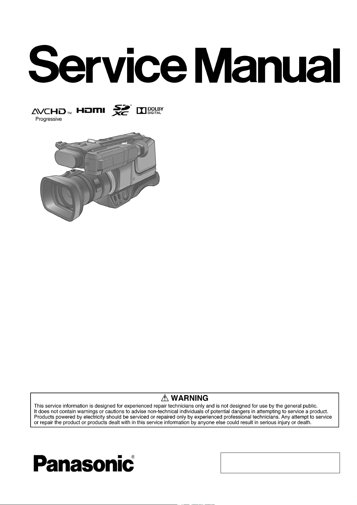
High Definition Video Camera
Model No. HC-MDH2GC
HC-MDH2GK
HC-MDH2MGC
Colour
(K)...........Black Type
© Panasonic Corporation 2013 Unauthorized copying and distribution is a violation of law.
Page 2

TABLE OF CONTENTS
PAG E PAG E
1 Safety Precautions -----------------------------------------------3
1.1. General Guidelines ----------------------------------------3
1.2. Leakage Current Cold Check ---------------------------3
1.3. Leakage Current Hot Check (See Figure. 1) --------3
2Warning--------------------------------------------------------------4
2.1. Prevention of Electrostatic Discharge (ESD)
to Electrostatically Sensitive (ES) Devices ----------4
2.2. Caution for AC Cord (For GC) --------------------------5
2.3. How to Replace the Lithium Battery -------------------6
3 Service Navigation------------------------------------------------7
3.1. Introduction --------------------------------------------------7
3.2. General Description About Lead Free Solder
(PbF) ----------------------------------------------------------7
3.3. How to Define the Model Suffix-------------------------7
3.4. Formatting----------------------------------------------------8
3.5. Baking of replacement IC and defective P.C.B.
------------------------------------------------------------------9
4 Specifications ---------------------------------------------------- 10
5 Location of Controls and Components------------------ 15
6 Service Mode ----------------------------------------------------- 23
6.1. Model/Destination Settings ---------------------------- 24
6.2. Lock Search History Indication ----------------------- 24
6.3. Power ON Self Check Result Display--------------- 25
6.4. Adjustment function for the Service ----------------- 26
6.5. Restore the backed up adjustment data------------ 27
6.6. Touch Panel Calibration -------------------------------- 28
7 Service Fixture & Tools --------------------------------------- 29
7.1. When Replacing the Main P.C.B. -------------------- 29
7.2. Service Position ------------------------------------------ 29
8 Disassembly and Assembly Instructions --------------- 30
8.1. Disassembly Flow Chart for the Unit ---------------- 30
8.2. P.C.B. Location ------------------------------------------- 31
8.3. Disassembly Procedure for the Unit ---------------- 32
9 Measurements and Adjustments -------------------------- 54
9.1. Electric Adjustment --------------------------------------54
10 Factory Setting--------------------------------------------------- 69
10.1. How To Turn On The Factory Settings? ------------ 69
10.2. What Is The Factory Settings? ----------------------- 70
11 Block Diagra m --------------------------------------------------- 71
11.1. Overall Block Diagram ----------------------------------71
11.2. Camera/System Control Circuit Block
Diagram----------------------------------------------------- 72
11.3. Video/Audio Process(1) Circuit Block Diagram--- 73
11.4. Video/Audio Process(2) Circuit Block Diagram--- 74
11.5. Lens Drive Circuit Block Diagram -------------------- 75
11.6. Power Supply Circuit Block Diagram---------------- 76
12 Wiring Connection Diagram --------------------------------- 77
12.1. Interconnection Diagram ------------------------------- 77
2
Page 3
1 Safety Precautions
1.1. General Guidelines
1. IMPORTANT SAFETY NOTICE
There are special components used in this equipment
which are important for safety. These parts are marked by
in the Schematic Diagrams, Circuit Board Layout,
Exploded Views and Replacement Parts List. It is essential that these critical parts should be replaced with manufacturer’s specified parts to prevent X-RADIATION,
shock, fire, or other hazards. Do not modify the original
design without permission of manufacturer.
2. An Isolation Transformer should always be used during
the servicing of AC Adaptor whose chassis is not isolated
from the AC power line. Use a transformer of adequate
power rating as this protects the technician from accidents resulting in personal injury from electrical shocks. It
will also protect AC Adaptor from being damaged by accidental shorting that may occur during servicing.
3. When servicing, observe the original lead dress. If a short
circuit is found, replace all parts which have been overheated or damaged by the short circuit.
4. After servicing, see to it that all the protective devices
such as insulation barriers, insulation papers shields are
properly installed.
5. After servicing, make the following leakage current
checks to prevent the customer from being exposed to
shock hazards.
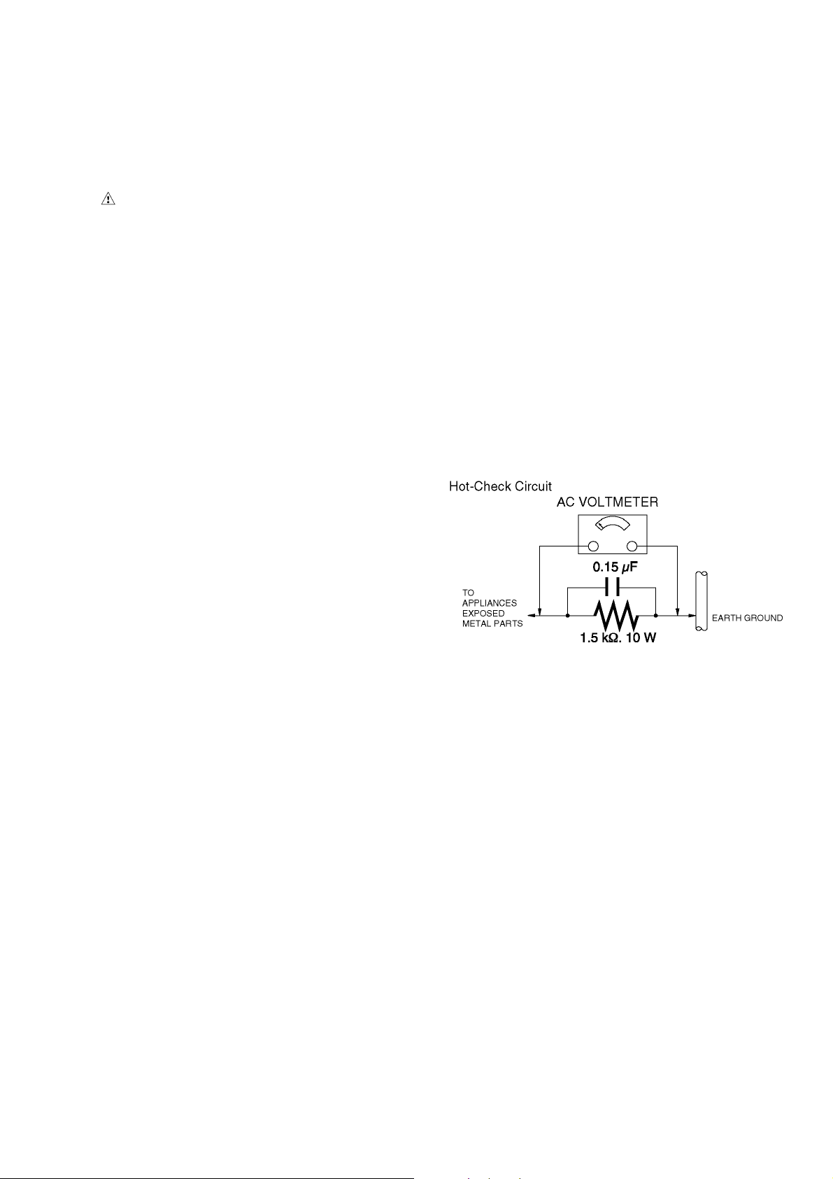
1.3. Leakage Current Hot Check (See Figure. 1)
1. Plug the AC cord directly into the AC outlet. Do not use
an isolation transformer for this check.
2. Connect a 1.5 kΩ, 10 W resistor, in parallel with a 0.15 μF
capacitor, between each exposed metallic part on the set
and a good earth ground, as shown in Figure. 1.
3. Use an AC voltmeter, with 1 kΩ/V or more sensitivity, to
measure the potential across the resistor.
4. Check each exposed metallic part, and measure the voltage at each point.
5. Reverse the AC plug in the AC outlet and repeat each of
the above measurements.
6. The potential at any point should not exceed 0.75 V RMS.
A leakage current tester (Simpson Model 229 or equivalent) may be used to make the hot checks, leakage current must not exceed 1/2 mA. In case a measurement is
outside of the limits specified, there is a possibility of a
shock hazard, and the equipment should be repaired and
rechecked before it is returned to the customer.
1.2. Leakage Current Cold Check
1. Unplug the AC cord and connect a jumper between the
two prongs on the plug.
2. Measure the resistance value, with an ohmmeter,
between the jumpered AC plug and each exposed metallic cabinet part on the equipment such as screwheads,
connectors, control shafts, etc. When the exposed metallic part has a return path to the chassis, the reading
should be between 1 MΩ and 5.2 MΩ. When the exposed
metal does not have a return path to the chassis, the
reading must be infinity.
Figure. 1
3
Page 4

2Warning
2.1. Prevention of Electrostatic Discharge (ESD) to Electrostatically Sensitive (ES) Devices
Some semiconductor (solid state) devices can be damaged easily by static electricity. Such components commonly are called Electrostatically Sensitive (ES) Devices. Examples of typical ES devices are integrated circuits and some field-effect transistors and
semiconductor “chip” components. The following techniques should be used to help reduce the incidence of component damage
caused by electrostatic discharge (ESD).
1. Immediately before handling any semiconductor component or semiconductor-equipped assembly, drain off any ESD on your
body by touching a known earth ground. Alternatively, obtain and wear a commercially available discharging ESD wrist strap,
which should be removed for potential shock reasons prior to applying power to the unit under test.
2. After removing an electrical assembly equipped with ES devices, place the assembly on a conductive surface such as aluminum foil, to prevent electrostatic charge buildup or exposure of the assembly.
3. Use only a grounded-tip soldering iron to solder or unsolder ES devices.
4. Use only an antistatic solder removal device. Some solder removal devices not classified as “antistatic (ESD protected)” can
generate electrical charge sufficient to damage ES devices.
5. Do not use freon-propelled chemicals. These can generate electrical charges sufficient to damage ES devices.
6. Do not remove a replacement ES device from its protective package until immediately before you are ready to install it. (Most
replacement ES devices are packaged with leads electrically shorted together by conductive foam, aluminum foil or comparable conductive material).
7. Immediately before removing the protective material from the leads of a replacement ES device, touch the protective material
to the chassis or circuit assembly into which the device will be installed.
CAUTION :
Be sure no power is applied to the chassis or circuit, and observe all other safety precautions.
8. Minimize bodily motions when handling unpackaged replacement ES devices. (Otherwise harmless motion such as the
brushing together of your clothes fabric or the lifting of your foot from a carpeted floor can generate static electricity (ESD) sufficient to damage an ES device).
4
Page 5
2.2. Caution for AC Cord (For GC)
2.2.1. Information for Your Safety
IMPORTANT
Your attention is drawn to the fact that recording of prerecorded tapes or discs or other published or broadcast
material may infringe copyright laws.
WARNING
To reduce the risk of fire or shock hazard, do not expose
this equipment to rain or moisture.
CAUTION
To reduce the risk of fire or shock hazard and annoying
interference, use the recommended accessories only.
FOR YOUR SAFETY
DO NOT REMOVE THE OUTER COVER
To prevent electric shock, do not remove the cover. No user
serviceable parts inside. Refer servicing to qualified service
personnel.
2.2.2. Caution for AC Mains Lead
For your safety, please read the following text carefully.
This appliance is supplied with a moulded three-pin mains plug
for your safety and convenience.
A 5-ampere fuse is fitted in this plug.
Should the fuse need to be replaced please ensure that the
replacement fuse has a rating of 5 amperes and it is approved
by ASTA or BSI to BS1362
Check for the ASTA mark or the BSI mark on the body of the
fuse.
2.2.2.1. Important
The wires in this mains lead are coloured in accordance with
the following code:
Blue Neutral
Brown Live
As the colours of the wires in the mains lead of this appliance
may not correspond with the coloured markings identifying the
terminals in your plug, proceed as follows:
The wire which is coloured BLUE must be connected to the terminal in the plug which is marked with the letter N or coloured
BLACK.
The wire which is coloured BROWN must be connected to the
terminal in the plug which is marked with the letter L or coloured
RED.
Under no circumstances should either of these wires be connected to the earth terminal of the three pin plug, marked with
the letter E or the Earth Symbol.
2.2.2.2. Before Use
Remove the Connector Cover as follows.
If the plug contains a removable fuse cover you must ensure
that it is refitted when the fuse is replaced.
If you lose the fuse cover, the plug must not be used until a
replacement cover is obtained.
A replacement fuse cover can be purchased from your local
Panasonic Dealer.
If the fitted moulded plug is unsuitable for the socket outlet in
your home then the fuse should be removed and the plug cut
off and disposed of safety.
There is a danger of severe electrical shock if the cut off plug is
inserted into any 13-ampere socket.
If a new plug is to be fitted please observe the wiring code as
shown below.
If in any doubt, please consult a qualified electrician.
2.2.2.3. How to Replace the Fuse
1. Remove the Fuse Cover with a screwdriver.
2. Replace the fuse and attach the Fuse cover.
5
Page 6
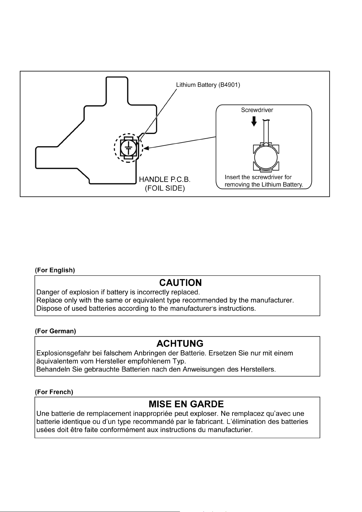
2.3. How to Replace the Lithium Battery
2.3.1. Replacement Procedure
1. Remove the HANDLE P.C.B.. (Refer to Disassembly Procedures.)
2. Remove the Lithium battery (Ref. No. “B4901” at foil side of HANDLE P.C.B.) and then replace it into new one
NOTE:
This Lithium battery is a critical component.
It must never be subjected to excessive heat or discharge.
It must therefore only be fitted in requirement designed specifically for its use.
Replacement batteries must be of same type and manufacture.
They must be fitted in the same manner and location as the original battery, with the correct polarity contacts observed.
Do not attempt to re-charge the old battery or re-use it for any other purpose.
It should be disposed of in waste products destined for burial rather than incineration.
NOTE:
Above caution is applicable for a battery pack which is for HC-MDH2/MDH2M series, as well.
6
Page 7
3 Service Navigation
3.1. Introduction
This service manual contains technical information, which allow service personnel’s to understand and service this model.
Please place orders using the parts list and not the drawing reference numbers.
If the circuit is changed or modified, the information will be followed by service manual to be controlled with original service manual.
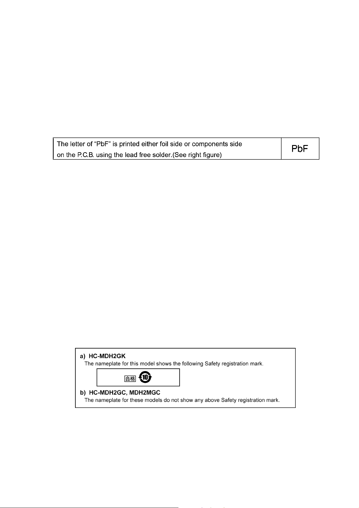
3.2. General Description About Lead Free Solder (PbF)
The lead free solder has been used in the mounting process of all electrical components on the printed circuit boards used for this
equipment in considering the globally environmental conservation.
The normal solder is the alloy of tin (Sn) and lead (Pb). On the other hand, the lead free solder is the alloy mainly consists of tin
(Sn), silver (Ag) and Copper (Cu), and the melting point of the lead free solder is higher approx.30°C (86°F) more than that of the
normal solder.
Distinction of P.C.B. Lead Free Solder being used
Service caution for repair work using Lead Free Solder (PbF)
• The lead free solder has to be used when repairing the equipment for which the lead free solder is used.
(Definition: The letter of “PbF” is printed on the P.C.B. using the lead free solder.)
• To put lead free solder, it should be well molten and mixed with the original lead free solder.
• Remove the remaining lead free solder on the P.C.B. cleanly for soldering of the new IC.
• Since the melting point of the lead free solder is higher than that of the normal lead solder, it takes the longer time to melt the
lead free solder.
• Use the soldering iron (more than 70W) equipped with the temperature control after setting the temperature at 350±30°C
(662±86°F).
Recommended Lead Free Solder (Service Parts Route.)
• The following 3 types of lead free solder are available through the service parts route.
RFKZ03D01KS-----------(0.3mm 100g Reel)
RFKZ06D01KS-----------(0.6mm 100g Reel)
RFKZ10D01KS-----------(1.0mm 100g Reel)
Note
* Ingredient: tin (Sn) 96.5%, silver (Ag) 3.0%, Copper (Cu) 0.5%, Cobalt (Co) / Germanium (Ge) 0.1 to 0.3%
3.3. How to Define the Model Suffix
There are two kinds of HC-MDH2/MDH2M.
• a) HC-MDH2GK
• b) HC-MDH2GC, MDH2MGC
What is the difference is that the “INITIAL SETTING” data which is stored in Flash ROM mounted on Main P.C.B..
3.3.1. Defining methods:
To define the model suffix to be serviced, refer to the rating label and caution label which are putted on the Unit.
NOTE:
After replacing the MAIN P.C.B., be sure to achieve adjustment.
7
Page 8
3.4. Formatting
The page number in this chapter does not show the page number of this service manual.
8
Page 9
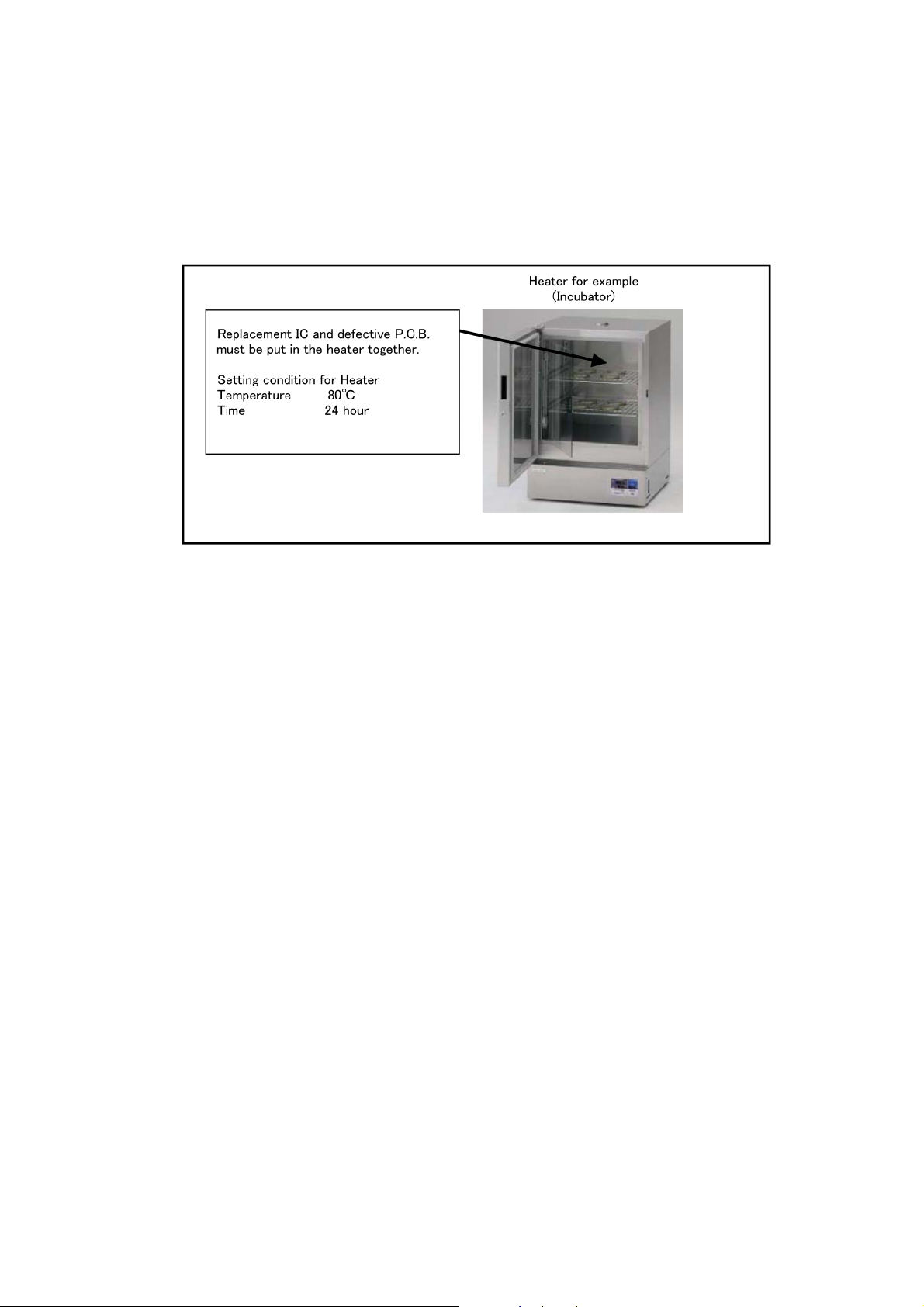
3.5. Baking of replacement IC and defective P.C.B.
When replacing the CSP/BGA/QFN type IC mounted on the P.C.B., the problem of IC crack or foil pattern breaking in the P.C.B.
might sometimes occur by rapid heating.
In order to improve the success rate of IC replacement for repair, it would be required to work out baking of replacement
IC and defective P.C.B. before replacing IC.
Please refer the way of baking as follows.
Replacement IC and defective P.C.B. must be put in the heater together.
• Baking temperature and time (Hour)
80°C / 24 hour
9
Page 10
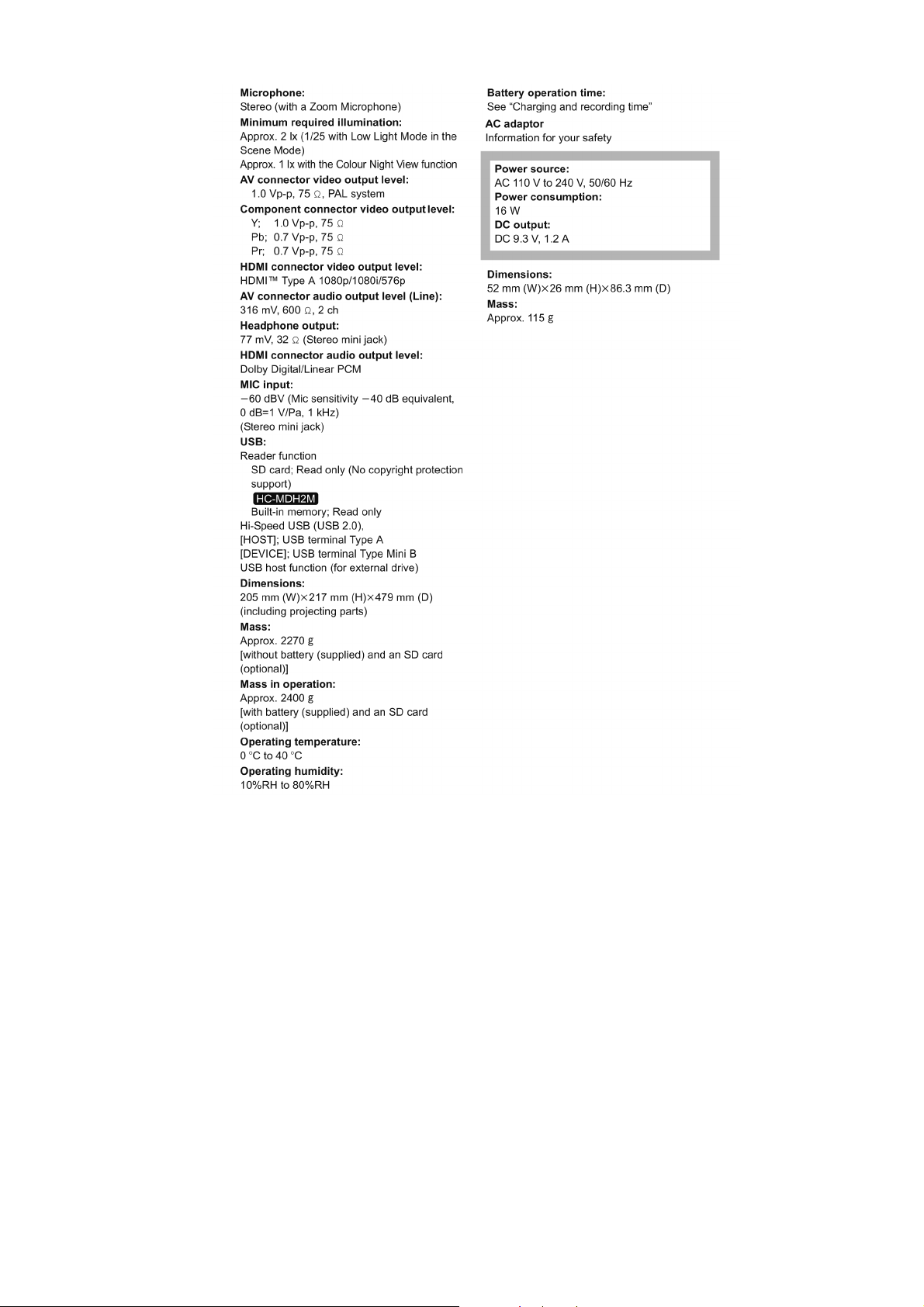
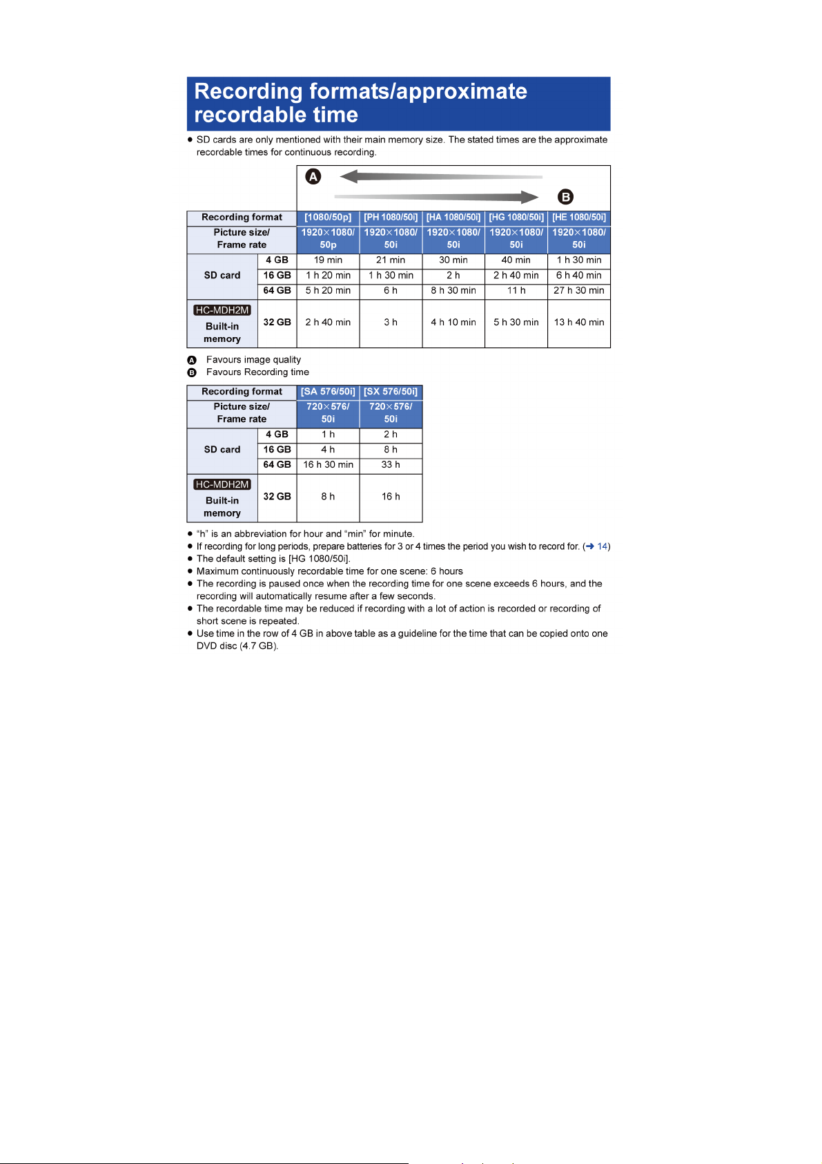
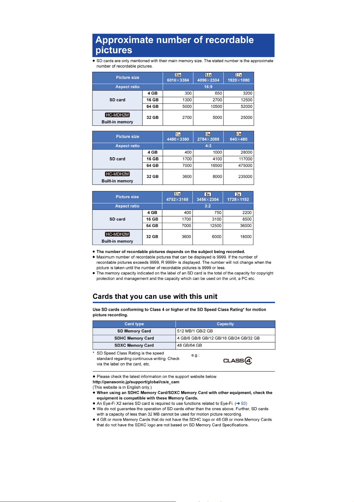
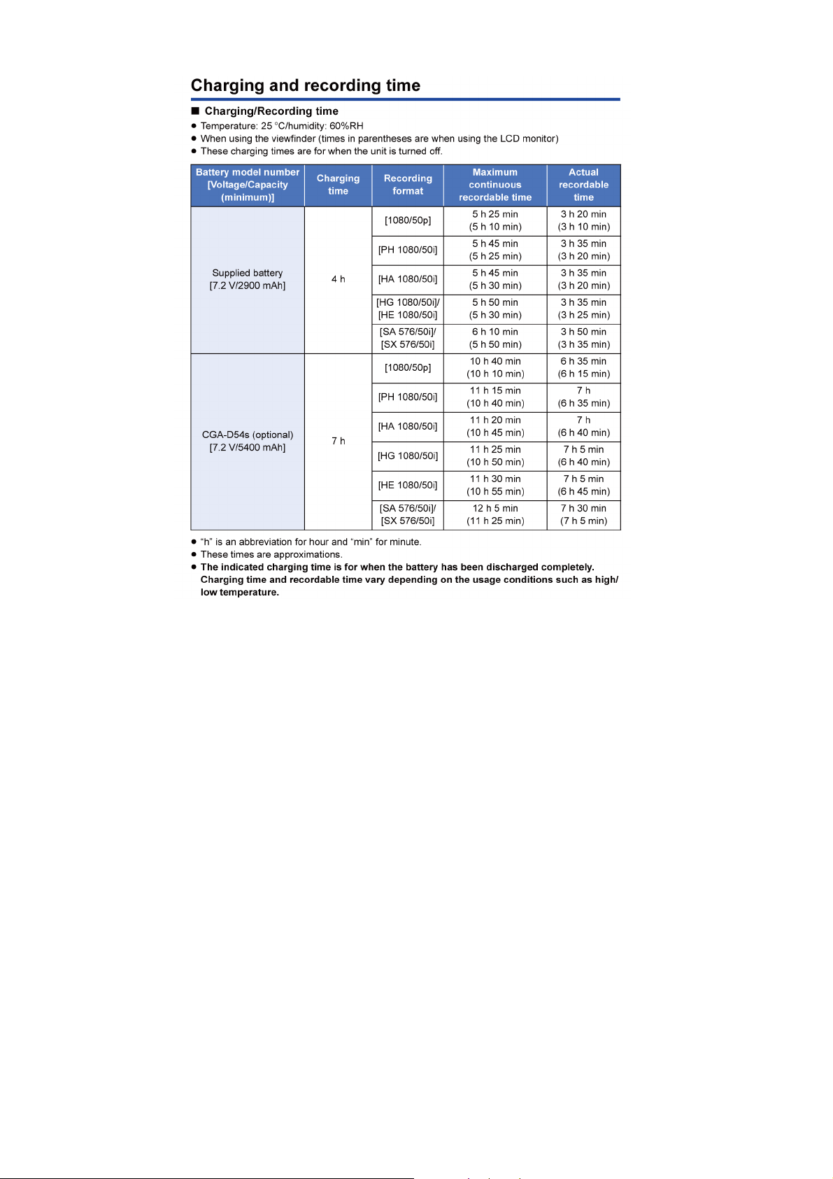
4 Specifications
The page number in this chapter does not show the page number of this service manual.
10
Page 11
1112131415
Page 12
Page 13
Page 14
Page 15

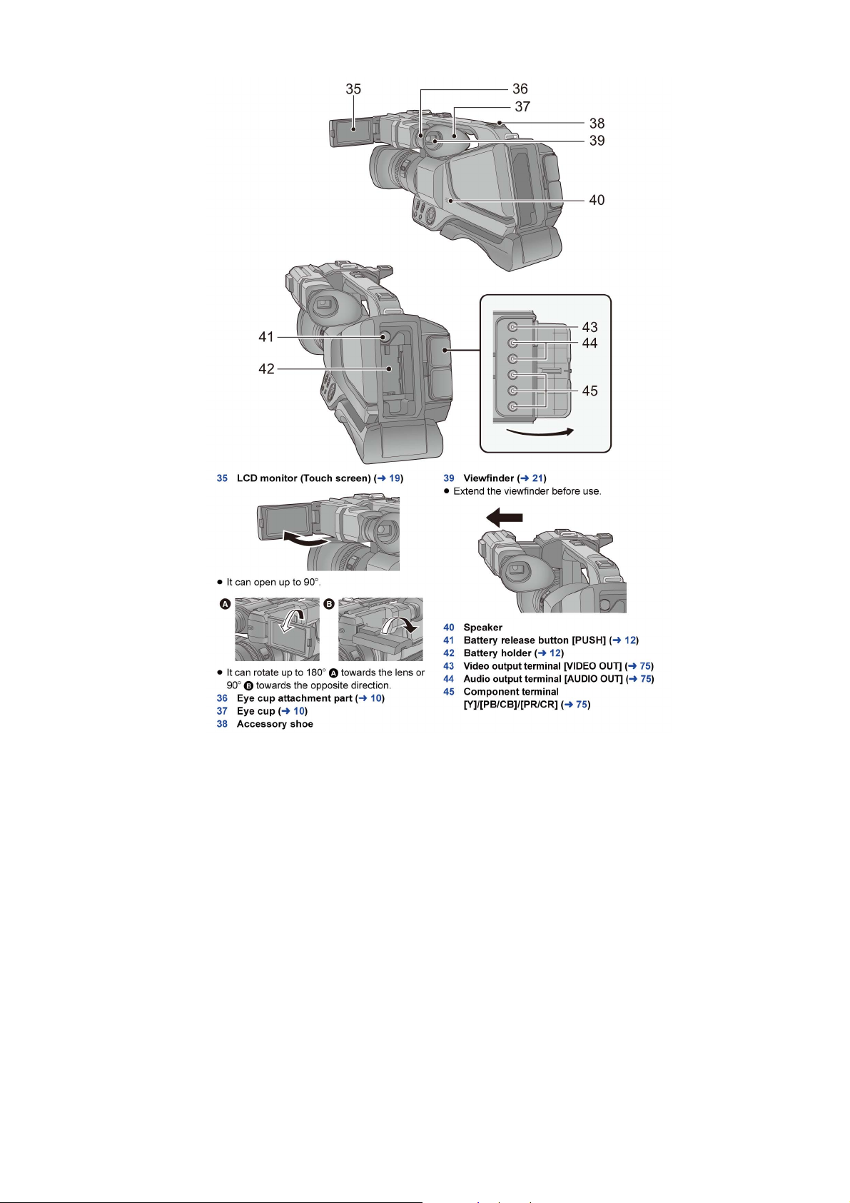
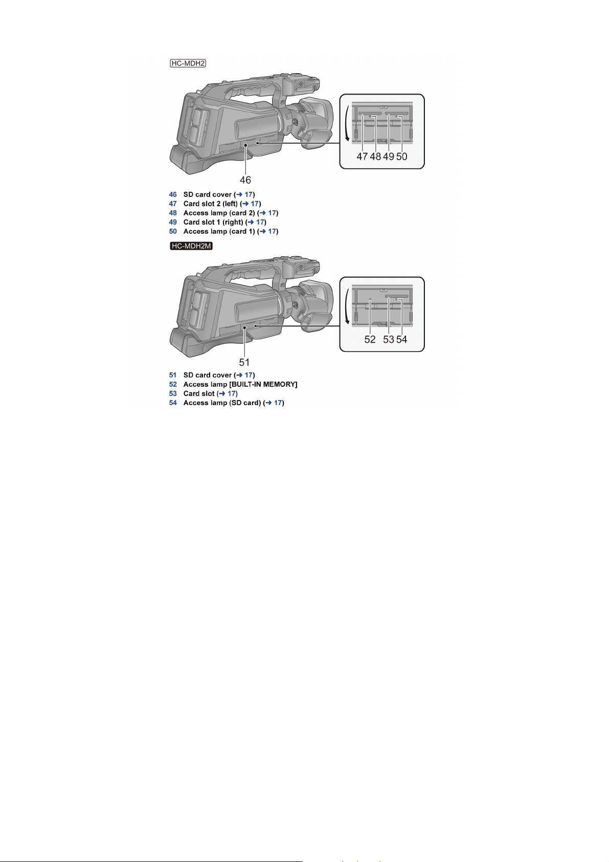
5 Location of Controls and Components
The page number in this chapter does not show the page number of this service manual.
Page 16
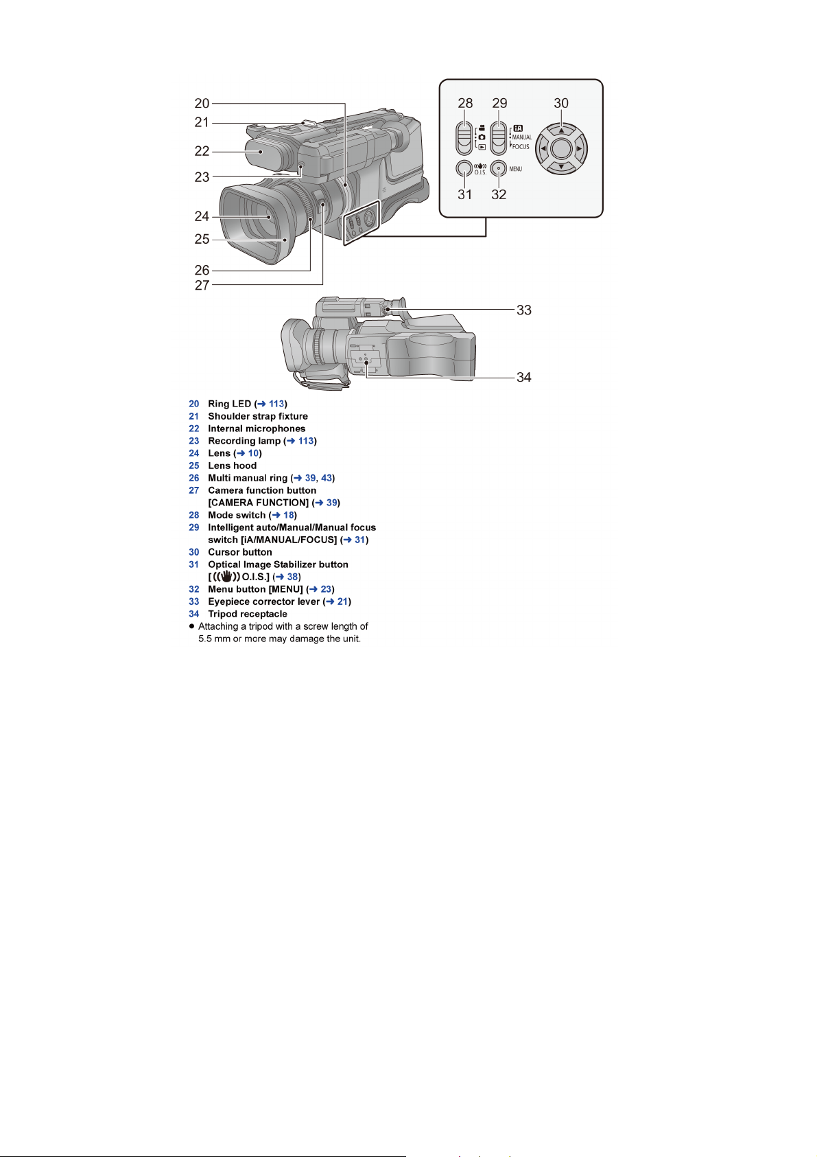
16171819202122
Page 17
Page 18
Page 19
Page 20
Page 21
Page 22

Page 23
6 Service Mode
Indication method of the service menu
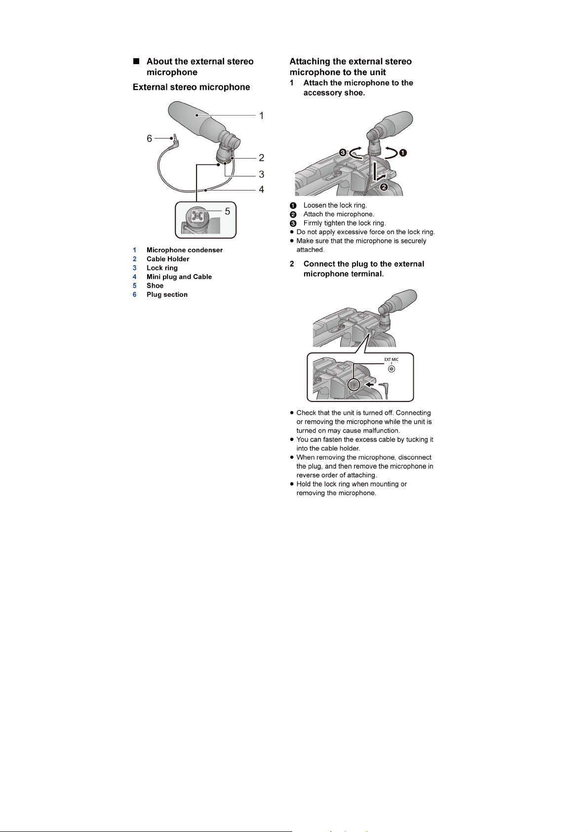
1. Set the mode switch “Motion Picture Recording” mode.
2. Set the power switch to ON, and turn to ON.
3. Keep pressing the “iA/MANUAL/FOCUS” switch to “FOCUS” side, “MENU” button and “Zoom Lever” (or “Sub Zoom Lever”)
to W side for more than 3 seconds until the top screen of the Service Mode Menu being displayed.
Service mode menu
Screen display Contents Function
1 Factory settings Function to throw a product up in a factory shipment state.
2 Model/Destination settings Change the Model/Destination.
4 Lock search history indication Display the camera system error cord for three histories saved in
5 Power ON self check result display Power ON self check (function to diagnose correct function of the
14 Adjutment function for the service The service adjustment do setup and adjustment of the following
15 Restore the backed up adjustment data Restore the adjustment data to new or repaired Main P.C.B. from
16 Touch panel calibration Calibrate the touch positions of the touch panel.
(When recorded data in Built-in memory, “error display” is done.)
(Selectable models and destinations are displayed.)
EEPROM.
device and interface between devices) result display.
items required in the field service.
SD card that the data backed up from original Main P.C.B. before
repairs or replacement.
NOTE:
Do not using service mode except above table of Service mode menu.
4. End method of the top screen of the service mode menu
Touch the [ EXIT ] of LCD to end the service mode, and then POWER OFF.
23
Page 24

6.1. Model/Destination Settings
Touch the [ 2 ] of LCD, select model/destination.
Operation specifications
Function description
• Change the Model/Destination
Display the lists of model/distination which the unit can be changed.
Therefore in some cases, the model/destination that is currently set is only displayed.
Touch the [ BAK ] of LCD to end the service mode, and then POWER OFF.
6.2. Lock Search History Indication
Touch the [ 4 ] of LCD, select lock search history indication.
Operation specifications
Indication contents
• Lock search history indication
Display the camera system error cord for three histories saved in EEPROM.
• The error cord contents which are displayed
Error code Function
51 Focus control is abnormal
52 Zoom control is abnormal
53 OIS lens control is abnormal
54 Zoom control is abnormal (2)
Touch the [ BAK ] of LCD to end the service mode, and then POWER OFF.
24
Page 25

6.3. Power ON Self Check Result Display
Touch the [ 5 ] of LCD, select Power ON self check result display.
Operation specifications
Indication contents
• Power ON self check result display
Function to diagnose correct function of the device and interface between devices result display.
Display the following communication test result.
- Power IC : Communication test between IC3401 and IC2303
- Main IC : Communication test between IC3401 and IC3402
- WiFi IC : (Excluded)
- NFC IC : (Excluded)
Display other than “OK” are abnomalities of each lines.
Touch the [ BAK ] of LCD to end the service mode, and then POWER OFF.
25
Page 26

6.4. Adjustment function for the Service
Touch the [14] of LCD, select the adjustment function for the service.
Operation Specifications (until before the start of the adjustment)
Function description
The service adjustment do setup and adjustment of the following items required in the field service.
For a detailed content, such as the adjustment procedure, refer to “9 Measurements and Adjustments”.
• Model setting
• Setting of the file name for adjustment data backup to SD card.
• Execution of adjustment data backup to SD card
• Checking of Switches
• Zoom Lever adjustment
• Camera adjustment (Iris, Gyro, OIS and Missing pixels)
• Zoom Tracking adjustments
• Indoor White Balance Adjustment (CH-GAIN, PWM, WB)
• Outdoor White Balance Adjustment (PWM, WB)
• Level shot adjustment
Set the power switch to OFF and turn the unit off.
26
Page 27

6.5. Restore the backed up adjustment data
Touch the [15] of LCD, select restoring the backed up adjustment data from SD card to the unit.
Operation Specifications
Function description
Restore the adjustment data to new or repaired Main P.C.B. from SD card that the data backed up from original Main P.C.B.
before repairs or replacement.
To backup the adjustment data, use “6.4. Adjustment function for the Service”.
Restoring procedure
Set the power switch to OFF and turn the unit off.
27
Page 28

6.6. Touch Panel Calibration
Touch the [16] of LCD, select the calibration of touch panel.
Operation Specifications
Function description
Calibrate the touch positions of the touch panel.
Set the power switch to OFF and turn the unit off.
28
Page 29

7 Service Fixture & Tools
7.1. When Replacing the Main P.C.B.
After replacing the MAIN P.C.B., be sure to achieve adjustment.
7.2. Service Position
This Service Position is used for checking and replacing parts. (Extension cable is not use.)
29
Page 30

8 Disassembly and Assembly Instructions
8.1. Disassembly Flow Chart for the Unit
This is a disassembling chart.
When assembling, perform this chart conversely.
30
Page 31

8.2. P.C.B. Location
31
Page 32

8.3. Disassembly Procedure for the Unit
No. Item Fig. Removal
1 Lens Hood Unit
Lens Mask
2 Handle T Unit
Sholder Belt Angle
Frame
3 Handle Zoom P.C.B. (Fig. D5) Screw (F) x 2
4 Slide Case Frame
Slide Case-R Unit
5 LCD INT P.C.B. (Fig. D9) Screw (J) x 1
6 Slide Case-L Unit (Fig. D10) Screw (K) x 4
7 Slide Base Unit (Fig. D11) FP4901 (Flex)
8 Handle P.C.B.
LCD FFC
9 MIC Case Unit
Microphone Unit
10 Side Case-R Unit (Fig. D16) Screw (P) x 6
11 Speaker (Fig. D17) Screw (S) x 2
(Fig. D1) Screw (A) x 1
Lens Hood Unit
(Fig. D2) Screw (B) x 3
Lens Mask
(Fig. D3) Screw (C) x 6
Screw (D) x 2
Hooking part x 2
Handle T Unit
(Fig. D4) Screw (E) x 4
Sholder Belt Angle Frame
Flex
Handle Zoom P.C.B.
(Fig. D6) Screw (G) x 2
Slide Case Frame
(Fig. D7) Screw (H) x 5
Screw (I) x 1
FP852 (Flex)
Locking tab x 3
Slide Case-R Unit
(Fig. D8) (NOTE: When Installing)
FP851 (Flex)
FP853 (Flex)
PS851 (Connector)
Hooking part x 1
Locking tab x 1
LCD INT P.C.B.
Slide Case-L Unit
FP4903 (Flex)
Screw (L) x 6
Screw (M) x 1
(Fig. D12) Slide Base Unit
(Fig. D13) Screw (N) x 2
MIC Shoe Attach
Screw (O) x 2
FP4902 (Flex)
(Fig. D14) FP4904 (Flex)
Handle P.C.B.
Locking tab x 2
LCD FFC
(Fig. D15) Locking tab x 1
MIC Case Unit
MIC Cushion A
MIC Cushion B
MIC Cushion C
Microphone Unit
Screw (Q) x 6
Screw (R) x 4
Locking tab x 3
FP6007 (Flex)
Side Case-R Unit
SP Angle
P6951 (Connector)
Speaker
No. Item Fig. Removal
12 Ring LED R P.C.B.
Side-R OP P.C.B.
13 Cam FUNC P.C.B. (Fig. D20) P6601 (Connector)
14 Grip Unit (Fig. D21) Screw (X) x 3
15 SS GYRO P.C.B. (Fig. D22) Screw (Z) x 5
16 Zoom Photo P.C.B. (Fig. D23) Screw (a) x 2
17 Rear Case (Fig. D24) FP6701 (Flex)
18 BATT Catcher P.C.B. (Fig. D25) Screw (f) x 2
19 AV Jack P.C.B. (Fig. D26) FP4501 (Flex)
20 Ring LED L P.C.B.
ESD P.C.B. Unit
(HC-MDH2M only)
HDMI FPC Unit
Main P.C.B.
21 SD Holder P.C.B. (Fig. D31) Screw (n) x 3
(Fig. D18) Screw (T) x 1
FP6631 (Flex)
Ring LED R P.C.B.
P6951 (Connector)
P6952 (Connector)
Screw (U) x 6
(Fig. D19) Screw (V) x 5
Side-R OP P.C.B.
Screw (W) x 2
Cam FUNC P.C.B.
Screw (Y) x 5
FP6401 (Flex)
Grip Unit
FP6402 (Flex)
SS GYRO P.C.B.
Screw (b) x 1
Photo Shot Button
Hooking part x 2
Zoom SW Hold Frame
Screw (c) x 2
Zoom Lever
Zoom Lever Cussion(B)
Zoom Photo P.C.B.
P6701 (Connector)
Screw (d) x 1
Screw (e) x 2
Locking tab x 2
Rear Case
BATT Catcher P.C.B.
FP4502 (Flex)
Screw (g) x 4
AV Jack P.C.B.
(Fig. D27) Screw (h) x 2
Screw (i) x 1
FP6011 (Flex)
Ring LED L P.C.B.
(Fig. D28) Screw (j) x 3
Screw (k) x 2
FP6003 (Flex)
FP6004 (Flex)
FP6005 (Flex)
FP6008 (Flex)
P301 (Connector)
P6002 (Connector)
P6003 (Connector)
(Fig. D29) Screw (l) x 2
Flex
ESD P.C.B. Unit
(Fig. D30) Screw (m) x 3
Locking tab x 1
Main Frame
FP6002 (Flex)
HDMI FPC Unit
Main P.C.B.
Screw (o) x 2
Hooking part x 3
SD Holder P.C.B.
32
Page 33

No. Item Fig. Removal
22 Front Unit (Fig. D32) Screw (p) x 1
Screw (q) x 2
Front Unit
23 Front Case
MF Unit
24 Lens INT P.C.B.
Camera Lens Unit
25 MOS Unit
Lens Unit
IR Filter
26 2nd Stepping Motor
4th Stepping Motor
27 LCD Unit (Fig. D40) Screw (w) x 2
28 LCD Case-T
LCD Hinge Unit
29 LCD Panel Unit
Monitor P.C.B.
(Fig. D33) Hooking part x 2
Front Case
Screw (r) x 1
(Fig. D34) Connector
MF Unit
(Fig. D35) Locking tab x 2
Lens Frame-R Unit
Screw (s) x 1
Locking tab x 2
(Fig. D36) FP6108 (Flex)
Lens INT P.C.B.
Camera Lens Unit
Lens Frame-L Unit
(Fig. D37) Screw (t) x 3
Lens Unit
MOS Unit
MOS Cushion
IR Filter
(Fig. D38) Screw (u) x 2
Solder x 8 points
Convex x 1
2nd Stepping Motor
(Fig. D39) Screw (v) x 1
Solder x 6 points
Convex x 4
4th Stepping Motor
Locking tab x 2
Hooking part x 2
LCD Hinge Angle
LCD SW Lever
LCD SW Spring
Convex x 2
(Fig. D41) LCD Case-R Unit
LCD Unit
(Fig. D42) Screw (x) x 2
Locking tab x 8
LCD Case-T
(Fig. D43) FP901 (Flex)
LCD Hinge Unit
(Fig. D44) Screw (y) x 1
LCD Frame A
FP904 (Flex)
FP905 (Flex)
(Fig. D45) Locking tab x 2
LCD Case B
LCD Panel Unit
Locking tab x 2
Monitor P.C.B.
(Fig. D46) Reflection Sheet
Light Guide Plate
Diffusion Sheet
Prism Sheet B
Prism Sheet A
LCD Holder
33
Page 34

8.3.1. Removal of the Lens Hood Unit and Lens Mask
(Fig. D2)
(Fig. D1)
34
Page 35

8.3.2. Removal of the Handle T Unit and Sholder Belt Angle Frame
(Fig. D4)
8.3.3. Removal of the Handle Zoom P.C.B.
(Fig. D3)
(Fig. D5)
35
Page 36

8.3.4. Removal of the Slide Case Frame and Slide Case-R Unit
(Fig. D6)
(Fig. D7)
36
Page 37

(Fig. D8)
8.3.5. Removal of the LCD INT P.C.B.
8.3.6. Removal of the Slide Case-L Unit
(Fig. D9)
(Fig. D10)
37
Page 38

8.3.7. Removal of the Slide Base Unit
(Fig. D12)
8.3.8. Removal of the Handle P.C.B.
(Fig. D11)
(Fig. D13)
38
Page 39

8.3.9. Removal of the MIC Case Unit and Microphone Unit
(Fig. D14)
(Fig. D15)
39
Page 40

8.3.10. Removal of the Side Case-R Unit
8.3.11. Removal of the Speaker
(Fig. D16)
(Fig. D17)
40
Page 41

8.3.12. Removal of the Ring LED R P.C.B. and Side-R OP P.C.B.
(Fig. D18)
(Fig. D19)
8.3.13. Removal of the Cam FUNC P.C.B.
41
(Fig. D20)
Page 42

8.3.14. Removal of the Grip Unit
8.3.15. Removal of the SS GYRO P.C.B.
(Fig. D21)
(Fig. D22)
42
Page 43

8.3.16. Removal of the Zoom Photo P.C.B.
8.3.17. Removal of the Rear Case
(Fig. D23)
(Fig. D24)
43
Page 44

8.3.18. Removal of the BATT Catcher P. C .B .
8.3.20. Removal of the Ring LED L P.C.B., ESD P.C.B. Unit (HC-MDH2M only), HDMI FPC Unit and Main P.C.B.
(Fig. D25)
8.3.19. Removal of the AV Jack P.C.B.
(Fig. D26)
(Fig. D27)
44
Page 45

(Fig. D28)
(Fig. D30)
(Fig. D29)
45
Page 46

8.3.21. Removal of the SD Holder P.C.B.
8.3.22. Removal of the Front Unit
(Fig. D31)
(Fig. D32)
46
Page 47

8.3.23. Removal of the Front Case and MF Unit
(Fig. D34)
(Fig. D33)
47
Page 48

8.3.24. Removal of the Lens INT P.C.B. and Camera Lens Unit
(Fig. D35)
(Fig. D36)
48
Page 49

8.3.25. Removal of the MOS Unit, Lens Unit and IR Filter
8.3.26. Removal of the 2nd Stepping Motor and 4th Stepping Motor
(Fig. D37)
49
(Fig. D38)
Page 50

8.3.27. Removal of the LCD Unit
(Fig. D39)
(Fig. D40)
50
Page 51

(Fig. D41)
8.3.28. Removal of the LCD Case-T and LCD Hinge Unit
51
(Fig. D42)
Page 52

(Fig. D43)
8.3.29. Removal of the LCD Panel Unit and Monitor P.C.B.
(Fig. D45)
(Fig. D44)
52
Page 53

(Fig. D46)
53
Page 54

9 Measurements and Adjustments
9.1. Electric Adjustment
• Adjustment method is different from a conventional High definition video camera.
• An exclusive jig are necessary for electric adjustment.
• Connection method of the main unit and an exclusive adjustment jig as follows.
Figure of connection
Figure of image when adjustment
54
Page 55

Part Number of jig
1. Basic Jig
Item Contents
AC adaptor Bandled with camcorder
AC Cable Bandled with camcorder
2. Optical Jig for Camera Adjustment
Item Part number Remarks
Light box VFK1164TDVLB/RFKZ0523* Need external power supply: 12V ± 0.1V /1.8A or over
Collimator with focus chart VFK1164TCM02/VFK1164TCM03 Same as DSC
CC filter 3100K/5100K VFK1164CC10G Need 2 set. For indoor/outdoor white balance adjutment
C2 Filter 5100K VFK1164LBB2 For outdoor white balance adjustment
C8 Filter 5100K VFK1164LBB8 For outdoor white balance adjustment
ND Filter 0.1 3100K VFK1164ND01 For indoor white balance adjustment
ND Filter 0.6 3100K VFK1164ND06 For indoor white balance adjustment
Adjustment chart for Level Shot Bandled with this Manual For Level shot adjustment
* RFKZ0523 (same as DSC) is recommended.
55
Page 56

[Level Shot Adjutment Chart]
56
Page 57

9.1.1. About Light Box
When using VFK1164TDVLB Light Box
If using VFK1164TDVLB Light Box, remove the lens connection ring by loosing thumbscrew and three hexagon screws.
* RFKZ0523 Light Box has no lens connection ring.
How to remove the Front Hood
In order to utilize maximum of the diffusing surface of light box, some adjustment items need the distance between diffusing
surface of light box and camera body becomes several cent-meters.
Before the adjustments, remove the front hood of light box following steps below.
[ For VFK1164TDVLB Light Box ]
[ For RFKZ0523 Light Box ]
57
Page 58

9.1.2. Adjustment Items
Adjustment item as follows.
58
Page 59

9.1.3. Adjustment Procedure
All adjustments except “Touch Panel Calibration” and “Factory Setting” performs using “14 Adjustment function for the service” in
service mode menu.
“Touch Panel Calibration” is performed using 16 of service mode menu and “Factory Setting” is performed using 1, of service mode
menu. Refer to “6 Service mode” and “10 Factory Setting”.
[Execute adjustment function for service]
1. Set the mode switch “Motion Picture Recording” mode.
2. Set the power switch to ON, and turn to ON.
3. Keep pressing the “iA/MANUAL/FOCUS” switch to “FOCUS” side, “MENU” button and “Zoom Lever” (or “Sub Zoom Lever”)
to W side for more than 3 seconds until the top screen of the Service Mode Menu being displayed.
4. Touch the twice then touch the [14] of LCD.
5. Touch the [YES] of LCD.
59
Page 60

[Adjustment Procedure]
Adjustments and settings are performed following order:
1. Model setting
2. Filename setting for backup to SD card
3. Backing up adjustment data to SD card
4. Checking switches
5. Zoom lever adjustment
6. Camera adjustment (Iris, Gyro, OIS, Missing pixels compensation)
7. Zoom/tracking adjustment
8. Indoor white balance adjustment (CH GAIN, PWM, WB)
9. Outdoor white balance adjustment (PWM, WB)
10. Level shot adjustment
60
Page 61

616263646566676869
Page 62

Page 63

Page 64

Page 65

Page 66

Page 67

Page 68

Page 69

10 Factory Setting
10.1. How To Turn On The Factory Settings?
1. Set the mode switch “Motion Picture Recording” mode.
2. Set the power switch to ON, and turn to ON.
3. Keep pressing the “iA/MANUAL/FOCUS” switch to “FOCUS” side, “MENU” button and “Zoom Lever” (or “Sub Zoom Lever”)
to W side for more than 3 seconds until the top screen of the Service Mode Menu being displayed.
4. Touch the [ 1 ] of LCD.
5. Touch the [ YES ] of LCD.
6. After few seconds “END” is displayed or “ESD NODATA” as “NG” is displayed on LCD monitor. Cutting of battery connection
or AC power supply connection as a completion of the “FACTORY SETTINGS”.
(After recording at least once, even if the physical format of the build-in memory will be performed, “ESD NODATA” as “NG” is
indicated, but “FACTORY SETTINGS” is completed.)
Page 70

10.2. What Is The Factory Settings?
The factory settings clean up and/or refresh the following settings.
1. MENU, MODE, ADJUSTMENT VALUE.
2. Reset the folder number and file number of still pictures.
(Setting the folder number is 100, and file number is 0.)
3. Clear the time and date setting.
4. Initialize the VIERA Link Physical Address.
5. Confirm that the data area of built-in memory is cleared. (HC-MDH2M only)
6. Confirm that the built-in memory cappacity is correct. (HC-MDH2M only)
(Checking of the built-in memory mounting error.)
(HC-MDH2M)
If the “Factory Settings” is completed, physical format of the build-in memory is not performed, execute physical format according to
the following procedure.
The shipment setting position of switches and lever:
(After the factory settings, set the switches and lever as following table.)
Name Setting position
Mode switch Motion picture recording mode
iA/MANUAL/FOCUS switch [ iA ] position
Power switch [ Off ] position
Eyepiece corrector lever [ Shortsighted End ] position
70
Page 71

11 Block Diagram
HC-MDH2/MDH2M OVERALL BLOCK DIAGRAM
NOTE
: VIDEO SIGNAL
: AUDIO SIGNAL
: CLK or CONTROL LINE
IRIS
LENS(F1.8-3.5 21x)
IC701
LENS/OIS DRIVE
SD
CARD
ECM
OPERATION
TOUCH PANEL
SD
CARD
MOS IMAGE
SENSOR
HDMI
TERMINAL
ZOOM/
OIS
FOCUS
Analog
SPEAKER
Analog
IC6401
GYRO
SENSOR
(PIT/YAW)
IC751
GYRO
SENSOR
(ROLL)
IC3403
NAND
FLASH ROM/
512Mbit
IC3405
RESET
IC3951
USB
SELECTOR
IC3402
DDR SDRAM/
1Gbit
IC3401
MPEG CODEC
(SPICa)
LED LIGHT
X3402
OSC
(54MHz)
IC302
GATE IC
IC6411
DIGITAL
ACCELEROMETER
IC901
LCD COLOR
DRIVER
COLOR LCD
PANEL
IC3701
AVIO
INTERNAL MEMORY
/32GB
USB TERMINAL
MINI USB TERMINAL
(HOST)
(DEVICE)
IC301,304,703,704,1011,1421,1424,
1431,1471,1502,1601,2301,2302
REGULATOR/VOLTAGE DET./
POWER DISTRIBUTION SWITCH/
LOGIC IC/DC/DC CONVERTER
IC4802
MIC AMP
EXT.
MIC
Q4901-4904,
4907,4908
MIC AMP
Analog Analog
IC761
ROLL GYRO AMP
COLOR EVF
PANEL
DC IN
BATTERY
IC1001,1501
BATTERY CHARGER/
POWER CIRCUIT
IC2303
RTC
X2301
(32.768kHz)
COMPONENT
TERMINAL
Analog
Analog
Analog
VIDEO OUT
AUDIO OUT
Analog
HEADPHONE
TERMINAL
IC706
MOTOR
DRIVE
HC-MDH2M only
HC-MDH2 only
11.1. Overall Block Diagram
71
Page 72

11.2. Camera/System Control Circuit Block Diagram
HC-MDH2/MDH2M CAMERA/SYSTEM CONTROL CIRCUIT BLOCK DIAGRAM
IC3401
(MPEG CODEC)
FP905
X RIGHT
Y BOT
X LEFT
Y TOP
1
2
3
4
PW REG3V
PW REG3V
P29
N29
P31
P30
B28
C28
B29
A29
R30
QR3411 QR3413
QR3410
QR3412
TOUCH PANEL
IC902
(MAGNETIC SENSOR)
4
3
1
2
VDD
OUT
GND
NC
ADC02
S ADTPYRIGHT
S AD TPX BOT
S AD TPYLEFT
S AD TPX TOP
SEL2 ON LOW
SEL1 ON HI
SEL2 ON HI
SEL1 ON LOW
LCD RVS
ADC03
ADC04
GPIOB19
GPIOB21
GPIOB17
GPIOB22
GPIOB20
ADC01
QR3404
AJ30
LVACH1DOP
LVACH1DOM
LVACH2DOP
LVACH2DOM
LVACH3DOP
LVACH3DOM
LVACH4DOP
LVACH4DOM
LVACLKP
LVACLKM
AJ31
AH28
X3402
(54MHz)
5
1
4
32
IC302
(GATE IC)
CH301
PW MOS1.8VD
AH29
AH30
AH31
AG28
AG29
AG30
AG31
RL3401 RL3402 RL3403 RL3404
IC3405
(RESET)
XRST
4
VDD
PW REG3V
2
AB31
CKIN
AE1
GPIO11
AL29
GLVDL PORL
AF25
IC3403
(NAND FLASH ROM/512Mbit)
RP
17
54
55
VCC(CORE)
VCC(IO)
OUT
BUS283 A D1P
BUS283 A D1M
BUS283 A D2P
BUS283 A D2M
BUS283 A D3P
BUS283 A D3M
BUS283 A D4P
BUS283 A D4M
BUS283 A CKP
BUS283 A CKM
AF28
LVBCH1DOP
LVBCH1DOM
LVBCH2DOP
LVBCH2DOM
LVBCH3DOP
LVBCH3DOM
LVBCH4DOP
LVBCH4DOM
LVBCLKP
LVBCLKM
AF29
AE28
AE29
AF30
AF31
AE30
AE31
AD28
AD29
RL3405 RL3406 RL3407 RL3408
BUS283 B D1P
BUS283 B D1M
BUS283 B D2P
BUS283 B D2M
BUS283 B D3P
BUS283 B D3M
BUS283 B D4P
BUS283 B D4M
XVD CAM
HDL BUSY
AF24
XHD CAM
GPIOC0
AH22
S SENS SDO
GPIOC1
AF21
S SENS SCK
GPIOC2
AH21
S SENS CS
GPIOC4
AE20
E MOS RST
MOSCLK ON H
CLK54 MOS
BUS283 B CKP
BUS283 B CKM
BUS324 A D0P
BUS324 A D0M
BUS324 A D1P
BUS324 A D1M
BUS324 A D2P
BUS324 A D2M
BUS324 A D3P
BUS324 A D3M
BUS324A CKP
BUS324 A CKM
BUS324 B D0P
BUS324 B D0M
BUS324 B D1P
BUS324 B D1M
BUS324 B D2P
BUS324 B D2M
BUS324 B D3P
BUS324 B D3M
VD SENS
HD SENS
SDATA SENS
SCK SENS
SCS SENS
RST SENS
CLK54 MOS
BUS324 B CKP
BUS324 B CKM
PW REG1.8V
E POW RST
(From QR2301-C)
IC2303
(RTC)
7
6
SIO
5
SCK
CS
X2301
(32.768kHz)
3
2
XIN
14
SW2
S6401
POWER
CL2301
XOUT
S RTC DT
S RTC SCK
RTC CS
CL2302
CL2303
GPIOE1
GPIOE2
GPIOE9
GPIOE0
L31
L30
L29
H31
CH3403
IC6953
(LOGIC IC)
1
2
S/L
9
CK
S DATA SR2M
MODE SW2
MODE SW1
IAMNL SW2
IAMNL SW1
CAM FUNC SW
RING LED R2
S KEYDATA CK
S KEYDATA LD
QH
3
E
F
B
G
C
H
D
S6951
ENTER
4
S6954
UP
12
S6955
LEFT
5
S6957
MENU
13
S6958
RIGHT
6
S6959
OIS
14
S6960
DOWN
C16
B16
A16
[PLAY] [PHOTO] [MOVIE]
S6956
MODE
LCD SLIDE SW
LCD SLIDE SW
G10
B11
F10
[IA] [MNL] [MF]
S6953
iA/MANUAL/FOCUS
S6601
CAMERA FUNCTION
B8
AK10
GPIOF20
GPIOF13
GPIOF0
GPIOD4
GPIOF10
GPIOF23
GPIOF12
GPIOF11
GPIOF1
GPIOF2
C8
D6632
PW REG3V
QR3417
QR3421
RING LED
(RED)
RING LED B2
GPIOF22
A8
D6631
PW 5V
QR3418
QR3422
RING LED
(BLUE)
RING LED R1
START STOPSW
GPIOF19
GPIOF14
B9
D6642
PW REG3V
QR3403
QR3419
RING LED
(RED)
RING LED B1
CHARGE LED
TALLY LED
CARD SD2LED
CARD SD1LED
POWER LED
GPIOF21
F8
D6641
PW 5V
QR3416
QR3420
RING LED
(BLUE)
D3931
CARD
LED(2)
CARD
LED(1)
PW REG3V
QR3414
D3901
PW REG3V
QR3409
D851
PW REG3V
QR3415
D3953
CHARGE
LED
TALLY
LED
PW REG3V
QR3423
R29
AF10
GPIOB1
GPIOD6
GPIOB18
GPIOB5
GPIOB6
Y31
D6401
POWER
PW REG3V
QR3408
W30
W29
S851
D10
S6402
S/S
C10
HANDL SS SW
GPIOF18
S6681
SUB S/S
C9
HANDL TELESW
HANDL WIDESW
GPIOF16
S6682
TELE
G9
GPIOF17
S6683
WIDE
D9
S6692
PHOTO
PHOTO ZENOSI
GPIOF15
F9
MOS
UNIT
72
Page 73

11.3. Video/Audio Process(1) Circuit Block Diagram
HC-MDH2/MDH2M VIDEO/AUDIO PROCESS(1) CIRCUIT BLOCK DIAGRAM
MOS UNIT
CAMERA SECTION
IC3401
(MPEG CODEC)
INTERNAL MEMORY:32GB
SDDATA 2
SDDATA 3
SDCMD
SDCLK
CARD DET
PROTECT
SDDATA 1
SDDATA 0
7
8
9
1
2
5
10
12
D0
D1
D2
D3
CMD
CLK
C.DET
WP
11
D1N LCD
D1P LCD
ABCK1
SCL1
SDA1
Y
PB
AODAT
AODAT0
AIDAT0
CLK B1
D23
C22
B23
C23
B22
A23
F24
D24
AC4
G1
U3
M4
LPD0CLK
LPD0XCLK
LPD0CKE
LPD0CS
LPD0WE
LPD0CAS
LPD0RAS
P2 N4P1M3 N3 R4
LPD0BA1
LPD0BA0
T4 R3N2
AMCK
CLK12 M
ALRCK0 CLK LR0
A13
A12
A10
B10
MEMORY CONTROL
MAIN CPU
HDMI
CONTROL
CAMERA
DSP
H.264
MPEG2
JPEG
AC3/5.1CH
PROCESSOR
HDMI DMA I/F
CAMERA SIGNAL PROCESSOR
AUDIO DSP
AL7
AK7
D0P LCD
AL5
D0N LCD
AK5
CLKP LCD
AL6
AK11
AJ11
AL11
AE12
AF11
AIDAT
G20
F20
F21
G21
C20
C19
CLK+
CLK-
LCD LVDS1P
LCD LVDS1N
LCD LVDS0P
LCD LVDS0N
LCD LVDSCLKP
LCD LVDSCLKN
SDCLK2
SDCMD2
PW 3.2V
S AV CHG SCL
S AV CHG SDA
G HDYSDY
G PBSDC
VREF
GPIOD5
AJ10
B14
E AVIO RST
CLKN LCD
AK6
HS3901
(SD CARD CONNECTOR)
ABCK0
CLK B0
ALRCK1 CLK LR1
AE11
AF12
PR
A14
G PR
SDDATA2 0
BUS24 ESDT0-3
BUS24 SD1DAT0-3
CLK24 SD1CMD
CLK48 SD1CARD
E CARD SD1DET
E CARD SD1PRO
CLK24 SD2CMD
CLK48 SD2CARD
E CARD SD2DET
E CARD SD2PRO
SDDATA1 2
SDDATA1 3
SDCMD1
SDCLK1
HDD UNLOAD H
HDD ACC INFO
SDDATA1 1
SDDATA1 0
7
8
9
1
2
5
10
12
D0
D1
D2
D3
CMD
CLK
C.DET
WP
11
B19
A19
A21
B21
B20
A20
G17
F18
HS3931
(SD CARD CONNECTOR)
BUS24 SD2DAT0-3
SDDATA2 1
SDDATA2 2
SDDATA2 3
STREAM CONTROL
AJ30
LVACH1DOP
LVACH1DOM
LVACH2DOP
LVACH2DOM
LVACH3DOP
LVACH3DOM
LVACH4DOP
LVACH4DOM
LVACLKP
LVACLKM
AJ31
AH28
AH29
AH30
AH31
AG28
AG29
AG30
AG31
BUS283 A D1P
BUS283 A D1M
BUS283 A D2P
BUS283 A D2M
BUS283 A D3P
BUS283 A D3M
BUS283 A D4P
BUS283 A D4M
BUS283 A CKP
BUS283 A CKM
AF28
LVBCH1DOP
LVBCH1DOM
LVBCH2DOP
LVBCH2DOM
LVBCH3DOP
LVBCH3DOM
LVBCH4DOP
LVBCH4DOM
LVBCLKP
LVBCLKM
AF29
AE28
AE29
AF30
AF31
AE30
AE31
AD28
AD29
BUS283 B D1P
BUS283 B D1M
BUS283 B D2P
BUS283 B D2M
BUS283 B D3P
BUS283 B D3M
BUS283 B D4P
BUS283 B D4M
BUS283 B CKP
BUS283 B CKM
IC3402
(DDR SDRAM/1G-bit)
28 40
LPD0DQ0
LPD0DQ31
W3
M2
LPD0DM0
LPD0DM3
W4
L1
LPD0DQS0
LPD0DQS3
LPD0A0
LPD0A13
ADDRESS CTL SIG
17 26714 5259
62 71 72 85
DATA
DATA2+
DATA2-
DATA1+
DATA1-
DATA0+
DATA0-
HPD
SCL
SDA
CEC
CEC 0
1 8
72
FL6001
1
3
3 6
54
4
6
1 8
72
FL6002
7
9
13
3 6
54
10
12
15
16
19
PW 3.2V
JK6451
HDMI TERMINAL
AK18
TX2P
AK14
AJ13
CEC
HPD
AK13
SDA
AL13
SCL
AL18
TX2M
AK17
TX1P
AL17
TX1M
AK16
TX0P
AL16
TX0M
AK15
TXCP
AL15
TXCM
1
2
3
6
5
4
QR3402
Q3401
QR3401
To IC901
(LCD COLOR DRIVER)
To IC3701
(AVIO)
PW REG3V
VRO
B13
FROM INT XNFWP
C4
G8 E4
A3
C1
C2 D3D2
495356
DATA
47
IC3403
(NAND FLASH ROM/512Mbit)
33
36
29
18
13
11
19
8
21
CTL SIG
35
28
10
14
ADM0
ADM15
ECLK NFCYC
XECS0 XNFCE
XEWE XNFWE
XERE XNFRE
XAVD NFALE
3
2
JK3953
USB TERMINAL
(HOST)
D+
D-
AL25
AL24
DP
DM
G19
XATADMACK
PW VBUS
USB A D-
USB SEL
USB A D+
USB D-
USB D+
USB B D-
USB B D+
1
VBUS
R3954
3
2
JK3952
MINI USB TERMINAL
(DEVICE)
D+
D-
USB VBUS
USB DET H
1
VBUS
IC3951
(USB SELECTOR)
4
1D-
5
1D+
6
2D-
7
2D+
1
D+
S
2
D-
10
PW 3.2V
QR3405
QR3406
D17
ATAIORDY
FUSE RESISTOR:
(R3954)
Please check the Fuse Rsistor when an output
voltage does not output.
AL9
AK9
S DO LCD
S CS LCD
S CLK LCD
To LCD PANEL
EVF UNIT
VCLKO LCD
YCO LCD0
AJ9
CLK27 EVF
TMDS2P SP
HPDTCT 0
S CLK DDC 0
S DAT DDC 0
TMDS2N SP
TMDS1P SP
TMDS1N SP
TMDS2P 0
TMDS2N 0
TMDS1P 0
TMDS1N 0
TMDS0P SP
TMDS0P 0
TMDS0N 0
TMDS0N SP
TMDSCLKP SP
TMDSCLKP 0
TMDSCLKN 0
TMDSCLKN SP
BUS13 EVFYC0-7
S CLK EVF
SCSEVF
GPIOC3
AF20
GPIOD2
S CS EVF
AH1
AH6
AE6
S DO EVF
GPIOD0
GPIOD1
S CLK LCDEVF
S DO LCDEVF
YCO LCD7
S CS LCD
ESD P.C.B.
HC-MDH2M only
HC-MDH2 only
73
Page 74

HC-MDH2/MDH2M VIDEO/AUDIO PROCESS(2) CIRCUIT BLOCK DIAGRAM
F7
G7
H7
LCD
UNIT
F6
IC901
(LCD COLOR DRIVER)
R0
D0+
D0-
R1
R2
R3
H6
G5
H5
G6
R4
R5
R6
R7
B7
C6
C7
A7
G0
G1
G2
G3
D7
E6
H4
D6
G4
G5
G6
HS
G3
VS
G4
PCLK
E7
G7
OUTPUT
REGISTER
CONFIGURATION
AND
POWER MANAGEMENT
PROTOCOL PARSING,
PARITY DETECTION,
ADVANCED
FRAME MIXING,
SYNC WORD
DECODING
DESERIALIZER
G1
H1
D1+
D1-
C1
D1
CLK+
CLK-
TX/RX
XSD
LS0
PSEL0
FM
F/XS
FSS
LS1
PSEL1
E1
F1
F2
G2
D4
D3
D5
E5
E4
E3
PLL
FSS
0
1
DDR SDR
PW REG1.8V
C2
LCD LVDS1P
LCD LVDS1N
LCD LVDS0P
LCD LVDS0N
LCD LVDSCLKP
LCD LVDSCLKN
To IC3401
(MPEG CODEC)
To IC3401
(MPEG CODEC)
N x PCLK
S DO LCD
S CLK LCD
S CS LCD
G EXTMICL
G MIC OUT R
G MIC OUT L
EXT MIC
JK4901
EXT MIC L
(To IC3401-Y29)
MIC AMP
Q4901-4904,
4907,4908
+
-
+
-
ECM[L]
IC4802
(MIC AMP)
4
5
2
7
8
1
6
3
ECM[R]
Q4801
V-
V+
PW MIC5V
PW MIC5V
G EXTMICR
IC3701
(AVIO)
39
SDIN
50
I
2
C BUS
LOGIC
CHARGE
PUMP
AUDIO
CODEC
SCL
49
SDA
48
ADRSEL
47
PRST
23
32
CPBIN
29
PR IN
21
35
Y IN
16
CLAMP
MUTE
GCA
GCA
GCA
LPF
+
DAC0
ADC0
ADC1
ADC2
76
EVR
5
1
3
13
SP N
SP N
SP P
SP P
4
7
SPEAKER
VOL
HPOUT L
HPOUT R
VCOMHP
VCOMHP FB
HP DET L
(To IC3401-K31)
V PLUG IN H
(To IC3401-H29)
D PLUG IN H
(To IC3401-E30)
JK3951
(HEADPHONES)
HD/SD LPF
Pb/C LPF
Pr LPF
28
26
YLPOUT
YDRIN
HDY OUT
PB OUT
24
PR OUT
V OUT
G HDYSDY
G PBSDC
GPR
S AV CHG SCL
S AV CHG SDA
E AVIO RST
AODAT0
MUTE
LPF
LINEOUT L
GND AU
SPOUT2
SPOUT1
HPCOM
G HPR
G HPL
G VOUT
G HDYOUT
G PBOUT
G PROUT
G LOUT
G ROUT
78
VOL
LINEOUT R
EVR
+
+
79
PW SPK3.2V
VCC SP
LPFALC
LPF
ALC
LPF
ALC
LPF
ALC
LPF
ALC
LPF
ALC
DET
56
55
58
60
63
65
59
61
67
68
69
70
71
72
73
74
LINEIN R
LINEIN L
INT0 L
INT1 L
INT2 L
INT2 R
INT1 R
EXT1 L
EXT1 R
EXT2 L
EXT2 R
INT0 R
INT0 R2
INT0 L2
EXT0 L
EXT0 R
REG
10
11
12
14
PC1
GND P
PC2
VSS OUT
51
VREG
8
6
MUTE
TR
77
46
MCLK
BCLK1
41
40
WCLK1
CLK LR1
CLK B1
CLK12 M
SDOUT
38
AIDAT0
42
WCLK0
CLK LR0
BCLK0
44
CLK B0
RL3707
RL3706
RL3705
RL3704
RL3703
RL3702
RL3701
RL3708
RL3709
2
5
4
3
1
From/To IC3401
(MPEG CODEC)
JK4501
JK4502
CL4501
CL4502
PR OUT
P
B
OUT
Y OUT
AUDIO R
AUDIO L
VIDEO
11.4. Video/Audio Process(2) Circuit Block Diagram
74
Page 75

11.5. Lens Drive Circuit Block Diagram
HC-MDH2/MDH2M LENS DRIVE CIRCUIT BLOCK DIAGRAM
FILTER
MOS
M
4G ZOOM MOTOR
M
17
18
19
45
42
43
44
IC701
(LENS/OIS DRIVE)
4G ZAP
4GZAP LEN
4GZAN LEN
4GZBP LEN
4GZBN LEN
4G ZAN
4G ZBN
4G ZBP
16
1,2
4
5
3
2G ZAP
2G ZBP
IC3401
(MPEG CODEC)
M
IRIS MOT
FOCUS MOTOR
OR
FP6008
FP6008
2G ZBN
2G ZAN
2GZAP LEN
2GZBP LEN
PITDRV+ LEN
PITDRV- LEN
G PITHO+ LEN
G PITHI+ LEN
G PITHO+ LEN
2GZBN LEN
2GZAN LEN
13
HALL
SENSOR
HALL
SENSOR
OIS UNIT
FP6008
PITDRV+
PITDRV-
PITHO+
PITHIN+
PITHIN-
YAWDRV- YAWDRV- LEN
YAWDRV+ LEN
YAWDRV+
YAWHIN+
YAWHIN-
YAWHO- G YAWHO- LEN
G YAWHI+ LEN
G YAWHO+ LEN
34
33
30
29
28
31
22
21
26
27
24
25
PITHO-
YAWHO+
IRM+
IRM-
IRM+ LEN
IRM- LEN
FP6008
FP6008
IR HO+
IR HIN+ IRHIN+ LEN
IR HO-
IR HIN-
HALL
SENSOR
PMP
IRHOP
76
IRHON
31
71
YMP
PHON
28
YMN
70
24
PHOP
57
PHINP
PMN
77
27
IRHINP
55
IRMP
5
IRMN
8
ZAP
14
ZAN
17
ZBN
10
ZBP
13
AFAN
40
AFAP
73
YHON
74
56
YHOP
YHINP
PW GYRO3V
GCSB
GSCK
GSI
GSO
GYRO1
29
23
32
3
12
HD
NSCS
SCK
SDI(V2L)
SDO(L2V)
DAC LD
NPORI
HD225
STORM HD225
STORM VD60
STORM VD60
STORM HD225
SCK LEN
SDO LEN
GPIOE4
GPIOE8
GPIOE20
GPIOE5
GPIOE6
GPIOE7
VD60
22
VD
37
AFBN
38
40
FP6008
FMR B
FMR A G MRA LEN
G MRB LEN
G IRHO- LEN
G IRHO+ LEN
FOCUS
MR UNIT
MRA
65
MRB
68
33
AFBP
36
14
AL28
AK27
J30
J31
K29
CH711
CH713
CH712
CH718
CH719
CH720
15
1
80
49
SDI LEN
S LENDAT L2V
S LENDAT V2L
S SCK LEN
S NSCS LEN
NSCS LEN
DACLD LEN
S DACLD LEN
E LENS RST
E LENS RST L
S GYRO CSB
S GYRO SCK
S GYRO SI
S GYRO SO
G GYROR
G GYROR IN
G GYROREF
K30
J29
E29
CH721
CH722
CH723
(GYRO SENSOR:PIT/YAW)
11
MOSI
44
10
MISO
26
8
CSB
CL6401
CL6406
CL6411
CL6412
CL6403
CL6404
35
9
SCLK
CL6402
1
VCC
7
VDD
PW GYRO3V
IC751
IC6401
(GYRO SENSOR:ROLL)
IC761
(ROLL GYRO AMP)
48
NDHB
54
2
1
3
OUT
6
VREF
4
VCC
PW REG3V
IC6411
(DIGITAL ACCELEROMETER)
4
6
11
9
1
14
VDD
VS
8
CS
15
RESERVED
2GZOOM ENC
P 2GZABS LEN
4GZABS LEN
FP6008
10
7
9
6
11
4G ZLEDCONT
4G ZABS
2G ZABS
TOUT
QR775
2G ZLEDCONT
AA30
F31
2GZABS LEN
GPIOB0
GPIOE16
GPIOE15
GPIOE17
GPIOE18
GPIOE21
GPIOE22
F30
F29
P 4GZABS LEN
E31
LEDCONT LEN
36
35
FP6008
FMT+
FMT-
M
2G ZOOM MOTOR
4GZOOM ENC
CH715
CH714
CH717
CH716
4
IC706
(MOTOR DRIVE)
3
2
1
5
6
7
MREF
60
LIN PWM
6
VCC
QR773
Q773
PW LENS3.2V
CLK27LENS
CLK27 LENSCLK27 LENS
AL27
21
CK27M
SCL0
SDA/SDI/SDIO
INT1
INT2
SCL/SCLK
SDA0
N31
N30
MF RING1
MF RING2
S ACCEL SCL
S ACCEL SDA
PW LENS3R2V
MF SENSOR
D31
D30
8
PW REG3V
[TELE] [WIDE]
S6691
ZOOM
ZLEVER
ADC13
LENS TEMP
A25
75
Page 76

11.6. Power Supply Circuit Block Diagram
HC-MDH2/MDH2M POWER SUPPLY CIRCUIT BLOCK DIAGRAM
PGND12
CTL1235
CTL7
PGND12
LX2
PGND34
LX4
HX2
PGND34
HX3
LX3
LX6
PGND56
LX6
FB5
INV6
FB6
INV7
INV5
GND
FB4
INV4
INV3
FB3
INV2
FB2
SCP6
SCP6OUT
CMINUS
FB1
HVREG
CPLUS
VBAT
INV1
SCP
RT
VREGA
VCC
VREGD
PGND56
HX4
HX4
HX5
LX5
22 21 1820 1719 16 1525
HX1
26
LX1
27
LX1
28 24 23
34
35
36
37
38
39
CTL6
CTL4
LX4
40
41
42
29
30
31
32
33
11
12
13
14
10
9
8
7
6
5
4
3
2
1
46 47 48 49 5043 44 45
IC1001
(POWER)
PW HDM5V
CL1011
CL1391
CL1811
VBUS ON H
VOUT
NC
VIN
CONT
5
1
4
3
2
IC1011
(REGULATOR)
GND
PW 5V
PW MIC5V
LX7
HX6
PGND7
HX6
51 52 53 54
VO7
FB7
55 56
PW REG1.8V
PW 3.2V
CL1001
CL1311
CL1502
CL1101
CL1002
JK6701
1
3
4
2
+
T
D
-
JK3961
2
3
4
+
-
BATTERY
DC IN
Q1501
1
2
3
5
6
8
7
IC1501
(BATTERY
CHARGER)
20
1
2
3
4
5
15
14
19
18
17
6
7
8
9
ACN
ACP
CMRC
ACDRV
ACOK
LODRV
GND
VCC
PHASE
HIDRV
BTST
ACDET
IOUT
SDA
SCL
13
12
11
SRP
SRN
BATDRV
10
ILIM
16
REGN
IC3401
(MPEG CODEC)
IC1502
(LOGIC IC)
IC2303
(RTC)
12
CMP1
9
WKUP
10
CMP2
B10
A10
B25
13
SW1
1
3
2
INH
VEE
4
GND
COM
8
6
7
CH0
CH1
5
CTRL
VCC
QR1503
QR1504
QR1501
B4901
(LI BATT)
SDA1
SCL1
S AV CHG SDA
S AV CHG SCL
ADC12
CHG IOUT
BATT V
MICON D
IP6701
IP3961
QR1502
4
QR1101
CL1103
5
1
VOUTV
SS
CNT
4
NC
IC2301
(REGULATOR)
4
1
OUT
V
SS
2
V
DD
3
NC
IC2302
(VOLTAGE DET.)
3
VIN
QR2301
Q2301
2
BKUP
8
CL1504
CL1104
CL1105
CL1102
C27
A27
ADC07
ADC09
GPIOB4
GPIOB13
GPIOB12
BL PWM LCD
ADC08
QR1505
A26
MICON T
W31
LCDBL ON H
QR1001
QR1002
Q1002
QR1003
QR1291
CL1411
CL1321
CL1421
CL1424
PW SD3.2V
PW SPK3.2V
PW LENS3.2V
PW REG3V
Q1441
5
4
1 3
2
FUSE RESISTOR:
(R1001/R1291/R1601)
Please check the Fuse Rsistor when an output
voltage does not output.
R1601
PW MOS1.2V
CL1361
AF7
BL CONT
S RTC DT
S RTC SCK
RTC CS
POWER SW
U29
GPIOD3
AL10
VBUS OCP
MOSSENS ON H
T31
CL1331
IC703
(REGULATOR)
IC1471
(POWER
DISTRIBUTION
SWITCH)
PW LENS1.5V
1
2
3
6
8
7
IC1601
(DC/DC CONVERTER)
COMP
SS
4
5
FB
BOOT
SW GND
VIN
EN
PW VID1.1V
CL1601
CL1431
IC1431
4
1
3
2
VIN
VOUT
CE
GND
PW PLL1.1V
(REGULATOR)
4
1
3
2
VDD
VOUT
CE
GND
6
5
4
3
1
2
EN
IN
OUT
/FAULT
ILIM
GND
IC PROTECTOR:
(IP3961/IP6701)
Q1502
Q1504
Q1503
3
2
1 6
4
5
Q1505
Q1506
PW 5V
PW REG3V
7
6
5
SIO
SCK
CS
14
SW2
S6401
POWER
CL2302
CL2303
CL2301
X2301
(32.768kHz)
3
2
XIN
XOUT
GPIOE1
GPIOE2
GPIOE9
GPIOE0
L31
L30
L29
H31
CH3403
Q1091
QR1091
R1291
PW VBUS
NC
CTL
VOUT
VIN
5
1
4
3
2
IC1421
(REGULATOR)
GND
PW EVF2.5V
IC1424
(REGULATOR)
4
3
2
1
GND
CE
VIN
VOUT
PW MOS1.8VA
PW MOS1.8VD
PW GYRO3V
IC704
(REGULATOR)
4
3
2
1
GND
CE
VDD
VOUT
IC304
(REGULATOR)
4
3
2
1
GND
CE
VIN
VOUT
PW MOS3.3V
IC301
(REGULATOR)
4
3
2
1
GND
CE
IN
OUT
E POW RST
(QR3404-B)
D902-906
(LCD BACK LIGHT)
R1001
76
Page 77

HC-MDH2/MDH2M INTERCONNECTION DIAGRAM
MAIN P.C.B.
(COMPONENT SIDE)
:
(FOIL SIDE)
SD HOLDER P.C.B.
(FOIL SIDE)
:
(COMPONENT SIDE)
HANDLE P.C.B.
(COMPONENT SIDE)
:
(FOIL SIDE)
LCD INT P.C.B.
(COMPONENT SIDE)
LENS INT P.C.B.
(COMPONENT SIDE)
AV JACK P.C.B.
(FOIL SIDE)
SIDE-R OP P.C.B.
(FOIL SIDE)
ZOOM PHOTO P.C.B.
(FOIL SIDE)
RING LED R P.C.B
(FOIL SIDE)
RING LED L P.C.B.
(FOIL SIDE)
MONITOR P.C.B.
(FOIL SIDE)
BATT CATCHER P.C.B.
(COMPONENT SIDE)
:
(FOIL SIDE)
SS GYRO P.C.B.
(COMPONENT SIDE)
:
(FOIL SIDE)
CAM FUNC P.C.B.
(COMPONENT SIDE)
:
(FOIL SIDE)
45
43
41
39
37
35
33
31
29
27
25
23
21
19
17
15
13
11
9
7
5
3
1
44
42
40
38
36
34
32
30
28
26
24
22
20
18
16
14
12
10
8
6
4
2
2G ZAN
2G ZAP
FMR VCC
FMR GND
D GND
FMT+
PITDRV-
PITHIN-
PITHIN+
YAWHO+
YAWHO-
D GND
YAWDRV+
IRHIN+
IRHIND GND
IRM+
TOUT
2G ZABS
4G ZLEDCONT
4G ZBN
4G ZBP
4G ZAP
2G ZBP
2G ZBN
FMR B
FMR A
FMT-
PITDRV+
D GND
PITHO+
PITHO-
YAWHINYAWHIN+
YAWDRV-
D GND
IRHO+
IRHO-
IRM-
D GND
2G ZLEDCONT
2G&4GZENCVCC&TVCC
4G ZABS
4G ZAN
4G ZAP
FP6008
1
3
5
7
9
11
13
15
17
19
21
23
25
27
29
31
33
35
37
39
2
4
6
8
10
12
14
16
18
20
22
24
26
28
30
32
34
36
38
40
BUS283 A D1P
BUS283 A D1M
BUS283 A CKP
BUS283 A CKM
BUS283 A D2M
BUS283 A D2P
BUS283 A D3M
BUS283 A D3P
BUS283 A D4M
BUS283 A D4P
MCLK
D1.2V
D1.2V
D1.2V
SCS
SDI
RSTN
A1.8V
A1.8V
A3.3V
BUS283 B D4P
BUS283 B D4M
BUS283 B D3P
BUS283 B D3M
BUS283 B D2P
BUS283 B D2M
BUS283 B D1M
BUS283 B D1P
BUS283 B CKP
BUS283 B CKM
D1.8V
D1.8V
D1.2V
D1.2V
D3.3V
VD
HD
SCK
A3.3V
A3.3V
P301
2019181716151413121110
987654321
CLOCK
DATA0
DATA1
DATA2
DATA3
DATA4
DATA5
DATA6
DATA7
S DO EVF
S CS EVF
S CLK EVF
S CLK LCD
S DO LCD
D0 N
D0 P
CLK N
CLK P
D1 N
D1 P
PS6002
4543413937353331292725232119171513
11
97531
4442403836343230282624222018161412
10
864
2
TALLY LED
PW REG3V
PW REG1R8V
D GND
D GND
S AD TPX BOT
S AD TPX TOP
PW LCDBL L
PW LCDBL H
D GND
D GND
VDD2R5V
VCC5V
D GND
TELE (VREFH)
PW AUDIO10R5V
MIC GND
MIC GND
G EXTMICL
MIC OUT L
MIC GND
PW MIC5V
PW LIBATT
LCD SLIDE SW
PW REG3V
PW REG1R8V
D GND
S ADTPYRIGHT
S AD TPYLEFT
LCD RVS
PW LCDBL L
PW LCDBL H
D GND
S CS LCD
VDD2R5V
D GND
S/S
WIDE (VREFL)
PW AUDIO10R5V
MIC GND
G EXTMICR
MIC OUT R
MIC GND
EXTMIC L
PW MIC5V
FP6001
10
987654321
eSD1 VDD
eSD1 VDD
eSD1 D GND
eSD1 CLK
eSD1 D GND
eSD1 CMD
eSD1 DAT2
eSD1 DAT1
eSD1 DAT0
eSD1 DAT3
FP6010
4
3
2
1
BATT -
BATT +
ADP ADP +
P6003
16
14
12
10
8
6
4
2
15
13
11
9
7
5
3
1
G VOUT
G LOUT
G ROUT
A GND
D GND
D GND
HDYOUT
D PLUGIN H
V PLUGIN H
A GND
A GND
D
T
D GND
PROUT
PBOUT
FP6003
246
8
101214
16
13579
11
13
15
USB D+
D GND
B VBUS
A VBUS
USB SEL
HP DET L
G HPL
CHARGE LED
D GND
USB D-
D GND
A VBUS
A VBUS
D GND
G HPR
HPCOM
FP6005
246
8
1012141618202224262830
13579
11
131517192123252729
PW SD3R2V 1
PW SD3R2V 1
CARD SD2LED
E CARD SD2DET
E CARD SD2PRO
D GND
BUS24 SD1DAT2
BUS24 SD1DAT0
D GND
D GND
D GND
BUS24 SD2DAT3
BUS24 SD2DAT1
CLK48 SD2CARD
CLK24 SD2CMD
PW SD3R2V 1
PW SD3R2V 1
CARD SD1LED
E CARD SD1DET
E CARD SD1PRO
D GND
D GND
BUS24 SD1DAT3
BUS24 SD1DAT1
CLK48 SD1CARD
CLK24 SD1CMD
BUS24 SD2DAT2
BUS24 SD2DAT0
D GND
D GND
FP6004
22212019181716151413121110
987654321
SHIELD (D2)
SHIELD (D2)
DATA2+
DATA2 -
SHIELD (D1)
DATA1 +
DATA1 -
SHIELD (D0)
DATA0+
DATA0 -
SHIELD (CK)
CLK+
CLK-
CEC GND
CEC GND
CEC
SCL
SDA
+5V
HPD
D GND
D GND
FP6002
2018161412
10
864
2
191715
13
11
97531
RING LED R2
D GND
CAM FUNC SW
MODE SW1
IAMNL SW1
PW REG3V
S KEYDATA LD
S DATA SR2M
AUDIO VR1
SP OUT2
RING LED B2
D GND
D GND
MODE SW2
IAMNL SW2
D GND
S KEYDATA CK
AUDIO VR2
D GND
SP OUT1
FP6007
642
531
D GND
RING LED B1
RING LED R1
D GND
D GND
D GND
FP6011
432
1
PW LENS3R2V
MF RING1
MF RING2
D GND
P6002
1
3
5
7
9
11
13
15
17
2
4
6
8
10
12
14
16
18
ZOOM SW
PHOTO SW
S/S SW
D GND
D GND
GYRO GND
S GYRO SO
S GYRO CSB
S ACCEL SDA
PW REG3V
POWER LED
POWER SW
D GND
PW GYRO3V
S GYRO SI
S GYRO SCK
GYRO GND
S ACCEL SDL
FP6006
FP4901
454443424140393837363534333231302928272625242322212019181716151413
121110
987654321
PW LIBATT
PW MIC5V
PW MIC5V
EXTMIC L
MIC GND
MIC GND
MIC OUT L
MIC OUT R
G EXTMICL
G EXTMICR
MIC GND
MIC GND
MIC GND
PW AUDIO10R5V
PW AUDIO10R5V
WIDE (VREFL)
TELE (VREFH)
S/S
D GND
D GND
VCC5V
VDD2R5V
VDD2R5V
S CS LCD
D GND
D GND
D GND
PW LCDBL H
PW LCDBL H
PW LCDBL L
PW LCDBL L
LCD RVS
S AD TPX TOP
S AD TPYLEFT
S AD TPX BOT
S ADTPYRIGHT
D GND
D GND
D GND
PW REG1R8V
PW REG1R8V
PW REG3V
PW REG3V
LCD SLIDE SW
TALLY LED
FP4904
1
2
3
4
5
6
7
8
9
10
11
12
13
14
15
16
17
18
19
20
21
22
23
24
25
26
27
28
TALLY LED
LCD SLIDE SW
PW REG3V
PW REG3V
PW REG1R8V
PW REG1R8V
D GND
D GND
D GND
PW LIBATT
S ADTPYRIGHT
S AD TPX BOT
S AD TPYLEFT
S AD TPX TOP
LCD RVS
PW LCDBL L
PW LCDBL L
PW LCDBL H
PW LCDBL H
D GND
D GND
D GND
D GND
D GND
S CS LCD
VDD2R5V
VDD2R5V
VCC5V
531
642
GND (ZOOM AD)
GND
GND
WIDE (VREFL)
TELE (VREFH)
S/S
FP4903
FP4902
6
5
4
3
2
1
ECM R
ECM R
ECM GND
ECM GND
ECM L
ECM L
5
3
1
6
4
2
D GND
D
D GND
D GND
T
D GND
FP6701
2
1
BATT +
BATT -
P6701
13579
11
13
15
246
8
101214
16
G VOUT
G LOUT
G ROUT
A GND
A GND
A GND
HDYOUT
D PLUGIN H
V PLUGIN H
D GND
D GND
D
T
D GND
PROUT
PBOUT
FP4501
FP4502
12345
6
D GND
D GND
T
D
D GND
D GND
FP3901
302928272625242322212019181716151413121110
987654321
PW SD3R2V 1
PW SD3R2V 1
PW SD3R2V 1
PW SD3R2V 1
CARD SD1LED
CARD SD2LED
E CARD SD1DET
E CARD SD2DET
E CADD SD1PRO
E CARD SD2PRO
D GND
D GND
D GND
BUS24 SD1DAT2
BUS24 SD1DAT3
BUS24 SD1DAT0
BUS24 SD1DAT1
D GND
CLK48 SD1CARD
D GND
CLK24 SD1CMD
D GND
BUS24 SD2DAT2
BUS24 SD2DAT3
BUS24 SD2DAT0
BUS24 SD2DAT1
D GND
CLK48 SD2CARD
D GND
CLK24 SD2CMD
FP3902
16151413121110
987654321
D GND
D+
D-
D GND
D GND
B VBUS
A VBUS
A VBUS
A VBUS
USB SEL
D GND
HP DET L
G HPR
G HPL
HPCOM
CHARGE LED
1
2
PW ADP -
PW ADP +
P3961
2019181716151413121110
987654321
SP OUT1
SP OUT2
D GND
AUDIO VR1
AUDIO VR2
S DATA SR2M
S KEYDATA CK
S KEYDATA LD
D GND
PW REG3V
IAMNL SW2
IAMNL SW1
MODE SW2
MODE SW1
D GND
CAM FUNC SW
D GND
D GND
RING LED B2
RING LED R2
FP6951
642
531
D GND
RING LED B2
RING LED R2
D GND
D GND
D GND
FP6953
1
3
5
2
4
6
D GND
RING LED B2
RING LED R2
D GND
D GND
D GND
FP6631
6
4
2
5
3
1
D GND
D GND
D GND
RING LED R1
RING LED B1
D GND
FP6641
2
1
D GND
CAM FUNC SW
P6952
1
2
SP OUT1
SP OUT2
P6951
2
1
GND
CAM FUNC SW
P6601
1
3
5
2
4
6
PW REG3V
D GND
ZOOM GND
ZOOM AD
ZOOM GND
PHOTO SW
FP6691
18
17
16
15
14
13
12
11
10
9
8
7
6
5
4
3
2
1
ZOOM SW
PW REG3V
PHOTO SW
POWER LED
S/S SW
POWER SW
D GND
D GND
D GND
PW GYRO3V
GYRO GND
S GYRO SI
S GYRO SO
S GYRO SCK
S GYRO CSB
GYRO GND
S ACCEL SDA
S ACCEL SDL
FP6401
1
3
5
7
9
11
13
15
17
19
21
23
25
27
29
31
33
35
37
39
41
43
45
2
4
6
8
10
12
14
16
18
20
22
24
26
28
30
32
34
36
38
40
42
44
2G ZAN
2G ZBP
2G ZBN
FMR B
FMR A
FMT-
PITDRV+
D GND
PITHO+
PITHO-
YAWHINYAWHIN+
YAWDRV-
D GND
IRHO+
IRHO-
IRM-
D GND
2G ZLEDCONT
2G&4GZENCVCC&TVCC
4G ZABS
4G ZAN
4G ZAP
2G ZAN
2G ZAP
FMR VCC
FMR GND
D GND
FMT+
PITDRVPITHINPITHIN+
YAWHO+
YAWHO-
D GND
YAWDRV+
IRHIN+
IRHIN-
D GND
IRM+
TOUT
2G ZABS
4G ZLEDCONT
4G ZBN
4G ZBP
FP6201
13579
11
13151719212325272931333537
39
246
8
101214161820222426283032343638
2G ZAN
2G ZAP
FMR VCC
FMR GND
FMR A
FMT-
PITDRV+
PITHO+
PITHO-
YAWHIN-
YAWHIN+
YAWDRV-
IRHO+
IRHO-
IRM-
2G ZLEDCONT
2G&4GZENCVCC&TVCC
4G ZABS
4G ZAN
4G ZAP
2G ZBP
2G ZBN
FMR B
FMR GND
FMT+
PITDRV-
PITHIN-
PITHIN+
YAWHO+
YAWHO-
YAWDRV+
IRHIN+
IRHIN-
IRM+
TOUT
2G ZABS
4G ZLEDCONT
4G ZBN
4G ZBP
FP6108
1
2
3
4
X RIGHT
Y BOT
X LEFT
Y TOP
FP905
1
3
5
7
9
11
13
15
17
19
21
23
25
27
29
31
33
35
37
39
41
43
45
47
49
51
2
4
6
8
10
12
14
16
18
20
22
24
26
28
30
32
34
36
38
40
42
44
46
48
50
VGL
CP2M
CP3M
CP1P
DDVDH
CP1MX
CP5M
CP5PX
GND
VCOM
CP4AM
CP4BM
DCLK
HSYNC
DR6
DR4
DR2
DR0
DG6
DG4
DG2
DG0
GND
VCI
CSB
SDA
CP2P
CP3P
VGH
CP1M
CP1PX
CP5P
DDVDL
CP5MX
VCI
CP4AP
CP4BP
VCL
VSYNC
DR7
DR5
DR3
DR1
DG7
DG5
DG3
DG1
VPP MTP (OPEN)
IOVDD
VCORE
SCK
FP904 FP901
32
31
30
29
28
27
26
25
24
23
22
21
20
19
18
17
16
15
14
13
12
11
10
9
8
7
6
5
4
3
2
1
COIN BATT+
S ADTPYRIGHT
S AD TPX BOT
S AD TPYLEFT
S AD TPX TOP
LCD RVS
PW LCDBL L
PW LCDBL L
PW LCDBL H
PW LCDBL H
D GND
D GND
D GND
D GND
D GND
D GND
S CLK LCD
S CS LCD
S DO LCD
PW REG3V
D GND
D0 N
D0 P
D GND
CLK N
CLK P
D GND
D1 N
D1 P
D GND
PW REG1R8V
PW REG1R8V
13579
11
13151719212325
27
246
8
101214161820222426
VDD2R5
D GND
DATA0
DATA1
DATA2
DATA3
DATA4
DATA5
DATA6
DATA7
D GND
D GND
SEN
VCC5V
CLOCK
D GND
D GND
D GND
D GND
D GND
D GND
D GND
D GND
D GND
SCLK
SDAT
VCC5V
FP851
FP853
28272625242322212019181716151413121110
987654321
VCC5V
VDD2R5
VDD2R5
S CS LCD
D GND
D GND
D GND
D GND
D GND
PW LCDBL H
PW LCDBL H
PW LCDBL L
PW LCDBL L
LCD RVS
S AD TPX TOP
S AD TPYLEFT
S AD TPX BOT
S ADTPYRIGHT
D GND
D GND
D GND
D GND
PW REG1R8V
PW REG1R8V
PW REG3V
PW REG3V
LCD SLIDE SW
TALLY LED
PS851
123456789
1011121314151617181920
CLOCK
DATA0
DATA1
DATA2
DATA3
DATA4
DATA5
DATA6
DATA7
S DO EVF
S CS EVF
S CLK EVF
S CLK LCD
S DO LCD
D0 N
D0 P
CLK N
CLK P
D1 N
D1 P
13579
11
13151719212325272931333537
39
246
8
101214161820222426283032343638
PW REG1R8V
GNDNCGNDNCGNDNCGND
PW REG3V
S CS LCD
D GND
D GND
D GND
D GND
D GND
PW LCDBL H
PW LCDBL L
S AD TPX TOP
S AD TPX BOT
D GND
PW REG1R8V
D1 P
D1 N
CLK P
CLK N
D0 P
D0 N
PW REG3V
S DO LCD
S CLK LCD
D GND
D GND
D GND
D GND
PW LCDBL H
PW LCDBL L
LCD RVS
S AD TPYLEFT
S ADTPYRIGHT
FP852
123
4
+
T
D
-
JK6701
2
4
6
1
3
5
ZOOM GND
ZOOM GND
PW REG3V
PHOTO SW
ZOOM GND
ZOOM AD
FP6402
AV JACK FFC
ZOOM PHOTO FFC
USB AV FFC
SD FFC
DC BATT
CATCHER
WIRE UNIT
STEREO
MICROPHONE
HANDLE ZOOM UNIT
HANDLE FFC
LCD FFC
EVF UNIT
HANDLE WIRE UNIT
LCD HINGE UNIT
TOUCH PANEL
LCD
LCD UNIT
MOS UNIT
LENS UNIT
LENS INT FFC
SS GYRO FFC
FFC
SIDE-R OP FFC
SPEAKER
FFC
FFC
CAM FUNC WIRE UNIT
MF UNIT
ESD FFC
ESD P.C.B.
(INTERNAL MEMORY)
HC-MDH2M only
HDMI FPC UNIT
BATTERY
MF SENS WIRE UNIT
FFC
12 Wiring Connection Diagram
12.1. Interconnection Diagram
77
 Loading...