

Page 1
Panasonic Services Company
not designed for use by the general public. It does
National Training
TH-42PHD5/TH-50PHD5
TH-42PHW5/TH50PHW5
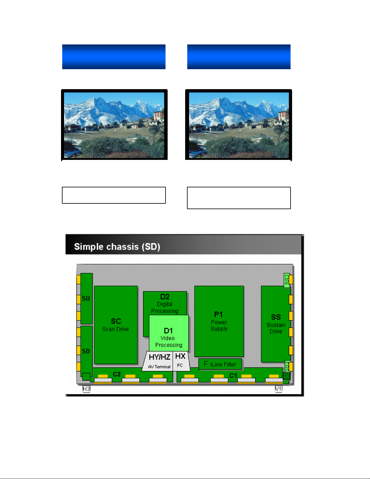
GPH5D Chassis
Plasma Display Panel
Troubleshooting Guide
This service information is designed for experienced repair technicians only and is
not contain warnings or cautions to advise non-technical individuals of potential dangers in attempting to service a product. Products
powered by electricity should be serviced or repaired only by experienced professional technicians. Any attempt to service or repair
the product or products dealt with in this service information by anyone else could result in serious injury or death.
Warning
Page 2

Objective...............................................................................................................5
2002 Model Line Up..............................................................................................6
Specifications.....................................................................................................7
Features.............................................................................................................8
New Asymmetrical Cell Structure Panel .........................................................9
Model Differences...........................................................................................9
Disassembly .......................................................................................................11
Rear Cover Removal .......................................................................................11
42” HD PCB Board Layout Diagram ...................................................................13
Printed Circuit Board Information Table...........................................................13
50” PCB Board Layout Diagram .........................................................................14
42” SD PCB Layout Diagram..............................................................................15
Video Signal Path Explanation............................................................................16
HY/HZ Board....................................................................................................16
HX Board .........................................................................................................17
D1 Board..........................................................................................................18
DVI Interface....................................................................................................19
Sync Process...................................................................................................21
RGB/PC Input Mode Sync ...............................................................................21
Composite/ Component Video Input mode Sync .............................................21
D1 Board.............................................................................................................22
D1 Main ICs Operation ....................................................................................22
D2 Board.............................................................................................................23
D2 Board details ..............................................................................................24
SC Board Explanation.........................................................................................25
SS Board Explanation.........................................................................................28
Power Supplies...................................................................................................31
Standby Power Supply.....................................................................................31
Main Power Supply..........................................................................................32
Power Factor Control....................................................................................32
Low Voltage Power supply............................................................................33
Voltage Regulation........................................................................................33
High Voltage Power Supply.............................................................................34
Protection Circuits...............................................................................................36
Diagnostic Procedures........................................................................................38
Self Check Display Indication...........................................................................38
Power LED Flashing timing chart.....................................................................39
Diagnostic Flow Charts.......................................................................................40
No Power.........................................................................................................40
The Power LED is red and blinking on/off........................................................41
Power LED blinks twice ...................................................................................42
No Picture Flowchart 1.....................................................................................43
No picture Flowchart 2.....................................................................................44
Dark picture Flowchart.....................................................................................45
Local screen failure.............................................................................................46
3
Page 3

Service Hints....................................................................................................46
After Image Prevention.......................................................................................53
Screen Saver Feature...................................................................................53
Side Bar Brightness adjustment....................................................................54
Option Setting.....................................................................................................55
Accessing the Option Menu.............................................................................55
Hidden Option Menu for GPH5D series...........................................................56
Sample Waveforms.............................................................................................58
HY/HZ board....................................................................................................58
HX board..........................................................................................................61
SC Board Input Signals....................................................................................63
SC Board Waveforms......................................................................................64
SS-Board Input Signals....................................................................................66
SS Board Waveforms ......................................................................................67
PDP Defect Pixel Specification...........................................................................68
Connector Tables................................................................................................69
F-BOARD CONNECTORS ..............................................................................69
P-BOARD CONNECTORS..............................................................................69
HX- BOARD CONNECTORS...........................................................................73
HY / HZ- BOARD CONNECTORS...................................................................74
Adjustment Procedures.......................................................................................75
Panel label Information....................................................................................75
+B Set-up.........................................................................................................76
Confirmation.....................................................................................................76
Driver Set-up....................................................................................................77
Initialization Pulse Adjust.................................................................................78
P.C.B. (Printed Circuit Board) exchange procedure.........................................79
Adjustment Volume Locations..........................................................................79
Test Point locations..........................................................................................80
Serviceman mode...............................................................................................81
CAT (computer aided test) Mode.....................................................................81
I2C Mode..........................................................................................................81
CD mode..........................................................................................................82
SD Mode..........................................................................................................83
I2C Menu Structure ..........................................................................................84
Alignment Procedures.........................................................................................85
NTSC Panel White Balance.............................................................................85
Pedestal Setting...............................................................................................86
PC/RGB Panel White Balance.........................................................................87
HD /525i /525P Panel White Balance ..............................................................89
625i Panel White Balance................................................................................91
Sub Brightness Setting ....................................................................................92
4
Page 4

Objective
The information provided in this document is designed to assist the technician in
determining the defective printed circuit board. The troubleshooting flow charts,
signal path charts and connector information should provide enough detail that
the technician can accurately determine which one of the printed circuit boards is
required to repair the product. Alignment and adjustment procedures are also
included in this document.
The Block diagrams and the schematic drawings reference the model TH42PHD5, but the technology is consistent with any GPH5D chassis.
5
Page 5
2002 Model Line Up
Digital Cinema Reality
Advanced 3-dimensional
1366 x 768 XGA Resolution
TH-50PHW5
50-inch (127 cm)
Wide Plasma Display
Plasma Contrast Automatic
Tracking System (C.A.T.S.)
3-Dimensional Progressive
VGA Resolution (UXGA
TH-42PW5
42-inch (106 cm)
HD Plasma Display
HD Panel
Progressive Scan
(UXGA Compatible)
Scan
Compatible)
TH-42PHW5
42-inch (106cm)
TH-37PW5
37-inch (94cm)
6
Page 6
Specifications
Our New 50” & 42” HD Progressive Panels
The industry’s highest-resolution panels
Panasonic Company PI Company F/H
Scanning Method Progressive Progressive
50-
inch
1,366 x 768=
1.05 million pixels
1,280 x 768=
0.98 million pixels
Interlace
N/A
Pixel
pitch
42/43-
inch
Pixel
pitch
Relationship between Picture resolution and Scanning method: 768p > 720p >
680p = 1080i > 1024i
0.810 (H) x 0.810 (V)
= 0.656
(42” Screen size)
1,024 x 768=
0.79 million pixels
0.898 (H) x 0.674 (V)
= 0.605
0.858 (H) x 0.808 (V)
= 0.693
(43” Screen size)
1,024 x 768=
0.79 million pixels
0.930 (H) x 0.698 (V)
= 0.649
1,024 x 5120.52
million pixels
0.90 (H) x 1.02 (V)=
0.918 / 2= 0.459
[1frame]
7
Page 7
Features
410,000
Pix
els
790,000
pixels
definition
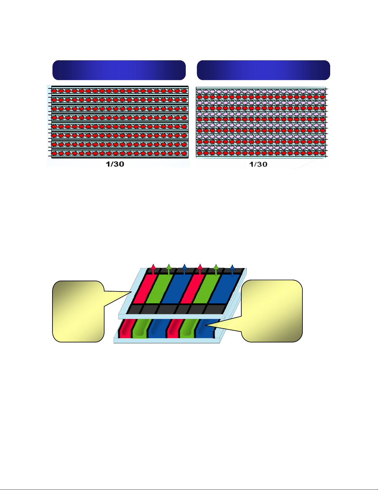
Pixel explanation
SD (Standard Definition) Panel
852 pixels
480 pixels
Provides the optimum number of pixels for viewing
standard broadcasts and DVD.
HD (High-Definition) panel
1,024 pixels
768 pixels
Reproduces even the tiniest details of high-
sources and other high-quality images.
Figure 1
8
Page 8
protection
filter glass
the natural
reproduction.
Scan Explanation
Panasonic progressive scan
Figure 2
The 1-field (1/60 sec) display pixels on the Panasonic 42" and 37" SD models
and on the ALIS system models are VGA level. (Panasonic HD models are XGA
level, for higher resolution.)
A.L.I.S. (Alternate Lighting of Surfaces) method is one of the new panel driving
systems of plasma display developed by Fujitsu Limited. ALIS method is a
system developed from the 3 electrode discharging system.
The ALIS method uses an interlaced driving scheme, which means the even and
odd lines are addressed alternately.
ALIS system Interlace scan
New front
improves
reds
New
phosphors
improve the
blue color
•
Figure 3
New Asymmetrical Cell Structure Panel
Figure 3 shows the unique asymmetrical cell structure that achieves both high
brightness and crisp whites. The asymmetrical arrangement of the red, blue and
green cells that control color reproduction results in a dramatically improved lightemitting balance of the three primary colors. This reproduces purer whites while
maintaining a high level of brightness.
Model Differences
9
Page 9
SSiinnggllee SSccaann ((SSDD))
DDuuaall SSccaann ((HHDD))
•Simple and low cost circuit
Figure 4
•High performance
•Higher brightness
10
Figure 5
Page 10
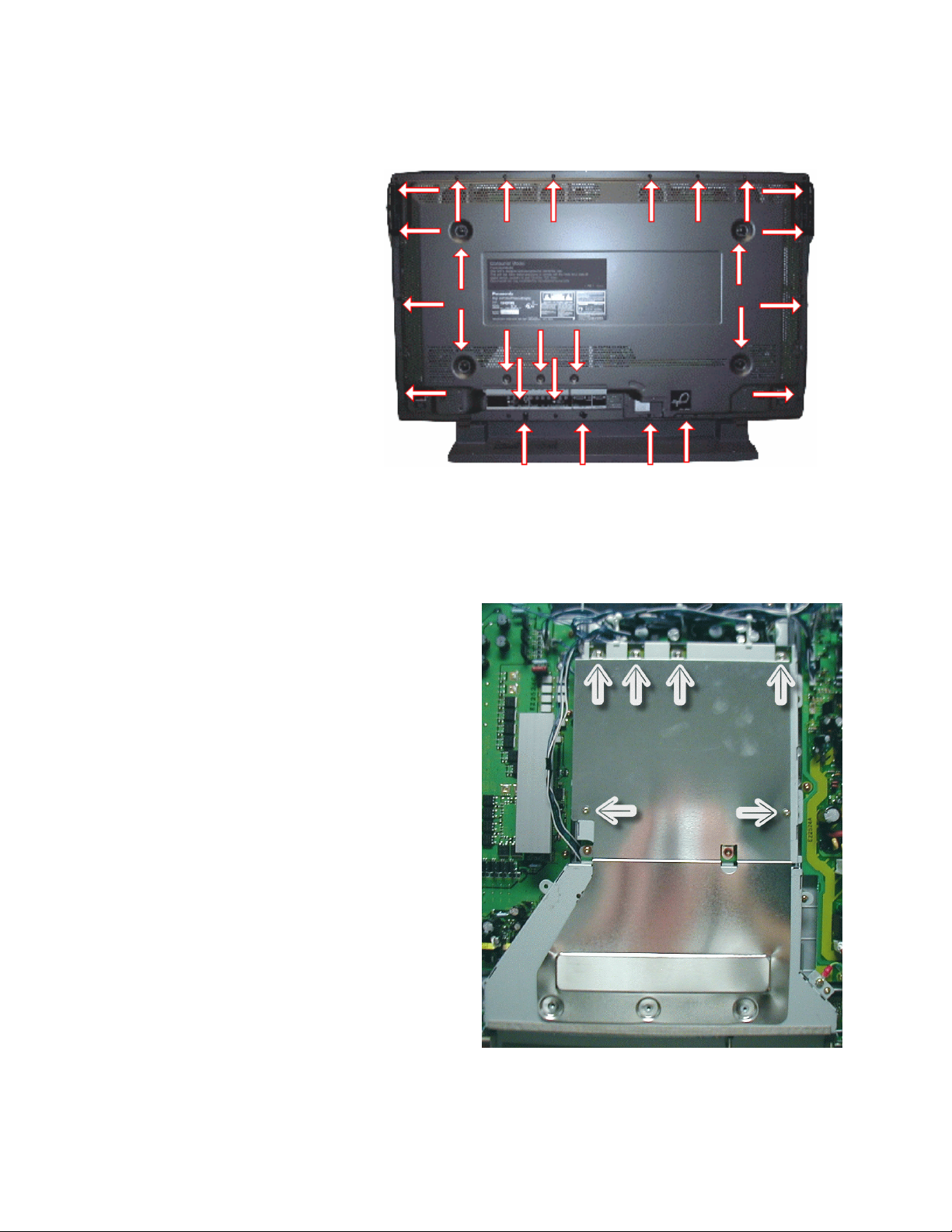
Disassembly
Rear Cover Removal
Remove the 27 screws,
shown in Figure 6, and
then pull away the rear
cover.
Removal of the shield
Remove the six screws, shown in
Figure 7, and then pull away the rear
shield cover.
Figure 6
11
Figure 8
Figure 7
Page 11
Location of Lead Wiring
Œ
Œ
Œ
Œ
Œ
Œ
Œ
Œ
•
•
High frequency
electromagnetic signals can
create electrical interference
within the unit. Be sure to
route all wires through their
respective harnesses
reference.
The chart below is an
illustration representing the
connectors and the wire
harnesses associated
Clamper Locations
Figure 9
with them.
Harness Number
Connector Number 1 2 3 4 5 6 7 8 9 10 11 12 13 14 15 16 17 18
Z6 è P6 Œ
Z10 è D10 Œ
Z17è D17 •
D12 èD22
D16 è D26
D25 è P5 Œ
D27 è P7 Œ
SC2 è P2 Œ Ž Œ Œ Œ Œ
SC4 è P4 Œ Ž Œ Œ Œ Œ
SC20 è D20 Œ
SC21è D21 Œ
H37è Z3 Œ Œ Œ Œ
H37 èZ4 Œ Œ Œ Œ Œ Œ Œ
SS1 èP1 •
SS3 èP3 Œ
SS32 èC32
SS42 èC42 Œ
ESC POWERè SS34 Œ
ESC V-BOARDè C44 Œ
F9 è P9
Fan 1 è P10 Œ Ž Œ
Fan 2 è P11 • • Œ
Fan 3 è P12 Œ Œ •
Fan 4 è P13 Œ Œ Œ
Œ Œ
Œ Œ
Œ
Œ Œ
Π= Wind the cable through the clamper once
• = Wind the cable through the clamper two times
Ž = Wind the cable through the clamper three times
12
Page 12
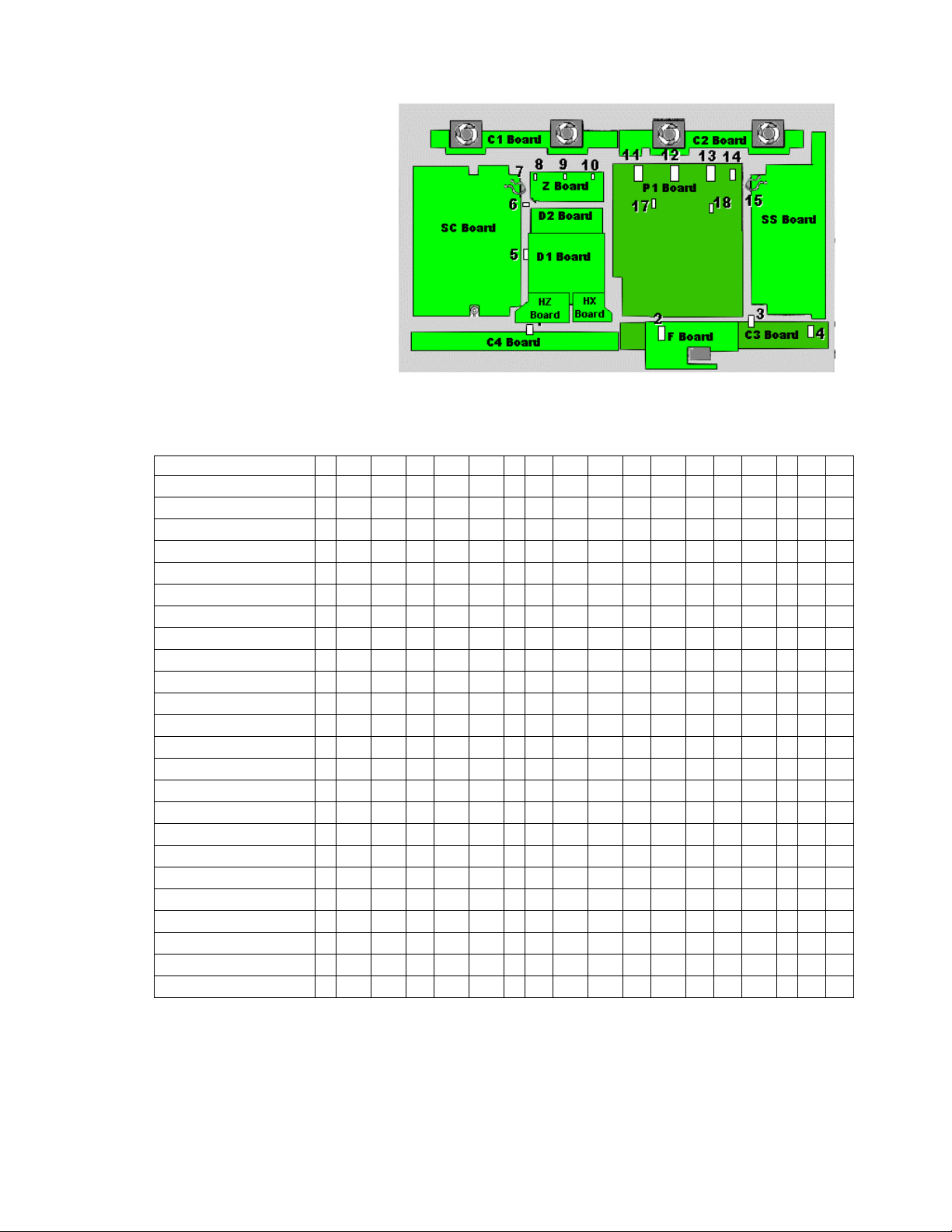
42” HD PCB Board Layout Diagram
Figure 10
Printed Circuit Board Information Table
Board Name Part Number Function
C1 TNPA2428 Data Drive (Upper Left)
C2 TNPA2429 Data Drive (Upper Right)
C3 TNPA2430 Data Drive (Lower Right)
C4 TNPA2431 Data Drive (Lower Left)
D1 TZTNP01LLSB Format Converter
D2 TNPA2427 Plasma AI Sub-Field Processor
F TNPA2444 Line filter
H3 TNPA2249 Speaker terminal
HX TZTNP01LLSU PC type Input terminal
HZ TXNHZ40JJS RCA type Input terminal
P TXN/P10LLS Power supply
P3 TNPA2439 Drive voltage oscillator
P5 TNPA2440 Primary oscillator
P6 TNPA2441 PFC oscillator
P7 TNPA2442 Drive voltage protection
P8 TNPA2443 Process voltage protection
S1 TNPA2283AC Power switch
SC TNPA2434 Scan out
SD TNPA2433 Scan connection (Lower)
SS TNPA2435 Sustain out
SS2 TNPA2436 Sustain connection (Upper)
SS3 TNPA2437 Sustain connection (Lower)
SU TNPA2432 Scan connection (Upper)
V1 TNPA2282AC Front SW. & Remote receiver
Z TNPA2445 Audio out
13
Page 13
50” PCB Board Layout Diagram
Board Name Part Number Function
C1 TNPA2510 Data Drive (Upper Left)
C2 TNPA2511 Data Drive (Upper Center)
C3 TNPA2512 Data Drive (Upper Right)
C4 TNPA2513 Data Drive (Lower Right)
C5 TNPA2514AB Data Drive (Lower Center)
C6 TNPA2515 Data Drive (Lower Left)
C9 TNPA2608 Energy Recovery Circuit
D1 TZTNP01MHSB Format Converter
D2 TNPA2427AB Plasma AI Sub-Field Processor
F TXN/F10MHS Line filter
H3 TNPA2249 Speaker Terminal
HX TZTNP02KESE PC type Input terminal
HZ TXNHZ40JJS RCA type Input terminal
P1 TXNP110MHS Power supply
P3 TNPA2566 Drive voltage oscillator
P5 TNPA2567 Primary oscillator
P6 TNPA2568 PFC oscillator
P7 TNPA2569 Drive voltage protection
P8 TNPA2570 Process voltage protection
S1 TNPA2283AC Power switch
SC TNPA2434AB Scan out
SD TNPA2518 Scan connection (Lower)
SS TXNSS10MHS Sustain out
SS2 TNPA2519 Sustain connection (Upper)
SS3 TNPA2520 Sustain connection (Lower)
SU TNPA2517 Scan connection (Upper)
V1 TNPA2282AC Front SW. & Remote receiver
Z TNPA2445 Audio out
Figure 11
14
Page 14
42” SD PCB Layout Diagram
Figure 12
Board Name Part Number Function
C1 TNPA2540 Data Drive (Lower Right)
C2 TNPA2541 Data Drive (Lower Left)
D1 TZTNP01MMSB Format Converter
D2 TNPA2589 Plasma AI Sub-Field Processor
F TXN/F10MMS Line filter
H3 TNPA2249 Speaker terminal
HX TZTNP020JAS PC type Input terminal
HZ TXNHZ40JJS RCA type Input terminal
P TNPA2598 Power supply
S1 TNPA2622 Power switch
SC TNPA2534 Scan out
SD TNPA2584 Scan Connection (Lower)
SS TNPA2535 Sustain Out
SS2 TNPA2536 Sustain Connection (Upper)
SS3 TNPA2537 Sustain Connection (Lower)
SU TNPA2583 Scan Connection (Upper)
V1 TNPA2621 Front SW. & Remote Receiver
Z TNPA2590 Audio out
15
Page 15
Video Signal Path Explanation
HY/HZ Board
Figure 13
The "HY/ HZ" board is equipped with one Component input, one Composite input
and one S-Video input. The Composite and S-Video inputs are applied to a
switching circuit, which is controlled by the system control IC, located on the D1Board. The switch select command is sent via the SCL3 and SDA3 lines. After
signal selection the composite or S-Video signals are amplified, buffered, and
applied to a 3D comb filter inside IC3803. The 3D Comb filter converts the
Composite input signals to Y, Pb, and Pr component signals. The output of
IC3804 is applied to the D1 Board via pins 1, 3, and 5 of the connector H2/D2.
Individual amplifiers buffered the Component input signals that are then applied
to the D1-Board via pins 15, 17, and 19 of the connector H2/D2. Vertical and
Horizontal Sync signals are also amplified on this board before they are applied
to the D1 Board.
16
Page 16
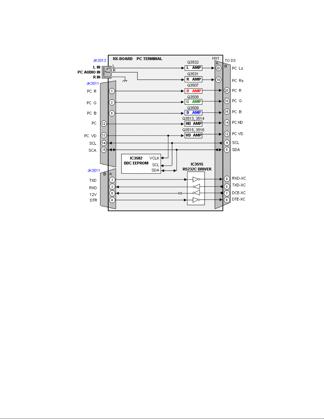
HX Board
Figure 14
PC RGB Signals are input to the HX Board. The RGB signals as well as the
vertical and horizontal sync signals are amplified by a series of transistor
amplifiers. The RS232C communications bus line is also connected on this
board. The RS-232C connection is provided so that operation changes can be
made via PC. An example of an application of this port would be remote turn on
of the unit for a kiosk or similar display.
The outputs of the HX board are applied to the D1 board via connector HX1/D3.
17
Page 17
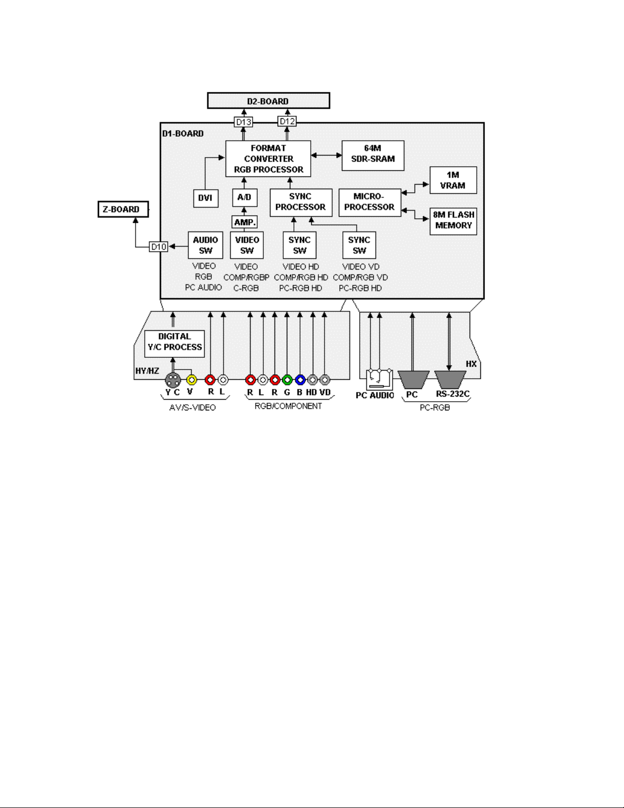
D1 Board
Figure 15
After the input signals are amplified by the HY/HZ and HX boards the desired
signal is selected. The microprocessor sends the command via the IIC bus to the
input select switch (IC3001). The video switch selects from one of the three
inputs. The component video signal output from the video switch is amplified and
converted to digital. An optional Digital Visual Interface (DVI) input bypasses the
A/D process as DVI information is already in the digital format.
Concurrently, the desired sync signals are selected and applied to the Sync
Processor. NTSC and Component sync signals are stripped from the Green
video component while the PC sync is applied directly. The Sync Processor
combines the On-Screen Display Sync signal with the input sync and converts
them to match the video format.
The corresponding audio signal is selected by an Audio switch and applied to the
Z board for further amplification
18
Page 18
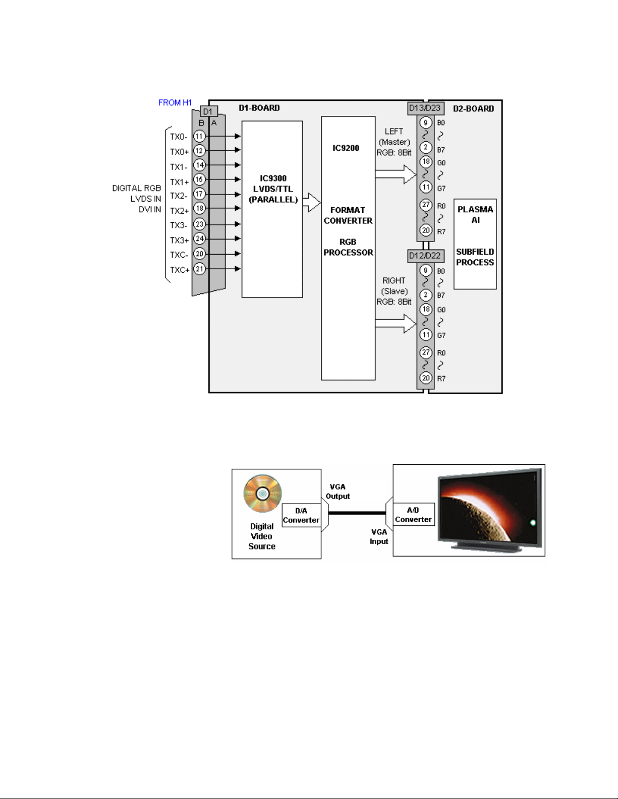
DVI Interface
Figure 16
An optional Digital Visual Interface (DVI) module connection is provided on this
generation Plasma Display Panels. The DVI interface allows direct digital transfer
from a display device to
the panel. A VGA or
component video signal
requires a conversion
from the digital to
analog and then
conversion back to
digital prior to input to
the Format converter see
Figure 17. The double
conversion can introduce
distortion to the signal.
Figure 17
19
Page 19
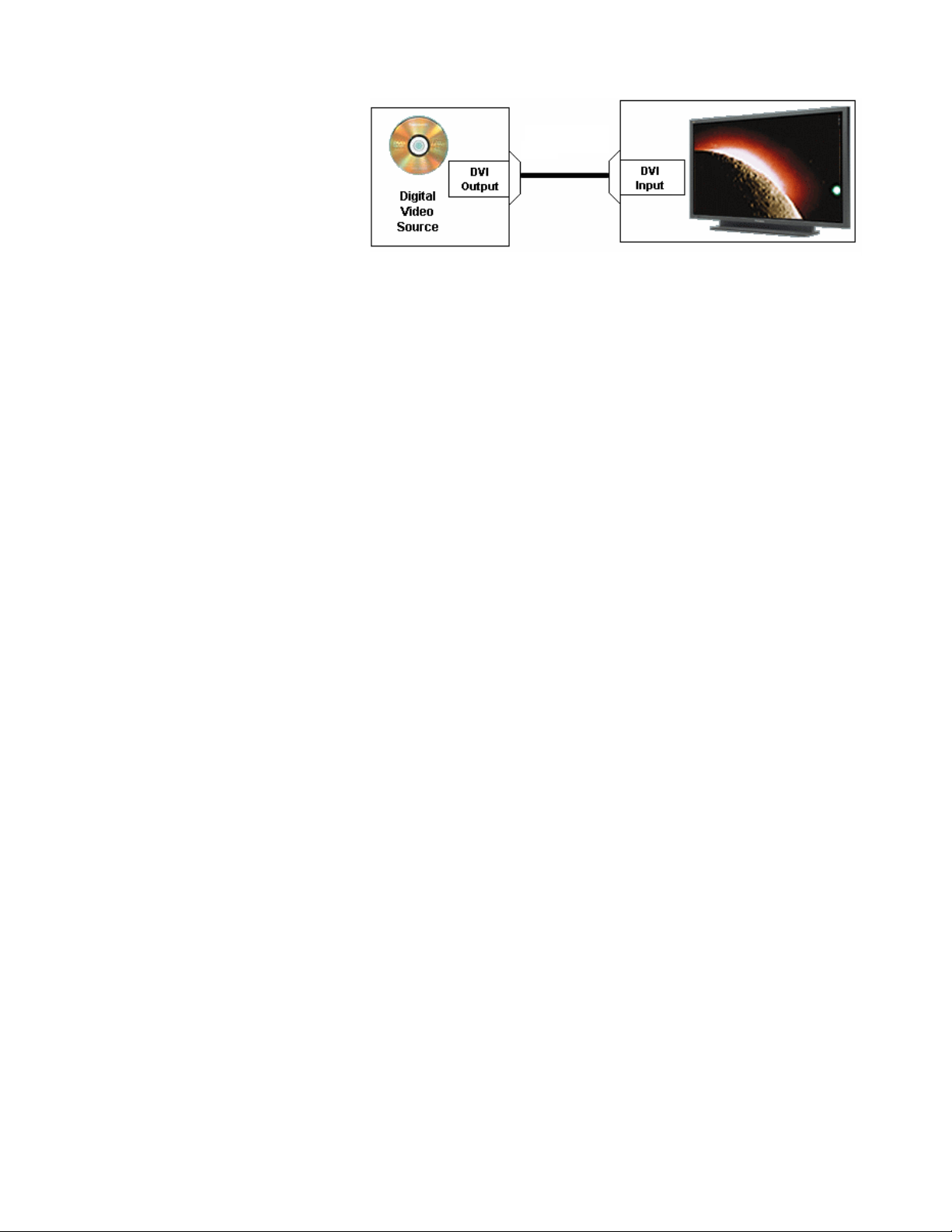
Figure 18 shows an
example of the DVI
interface. It permits direct
connection of the digital
video signal to the Format
converter. This bypasses
the D/A and A/D process
providing the better
quality picture.
Installation of the DVI interface requires removal of the HY/HZ Board and
replacing it with an optional DVI interface board.
Figure 18
20
Page 20
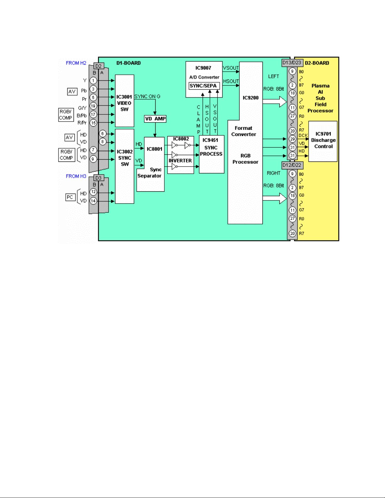
Sync Process
Figure 19
The vertical and horizontal sync signal paths are slightly different depending on
the Source signal.
RGB/PC Input Mode Sync
The vertical and horizontal sync signals generated by the input device are
applied to connector D3 or D2 to a Sync switch (IC3002). IC3002 outputs the
vertical and horizontal sync signals. The signals are inverted by IC8002 and then
applied to a sync processor (IC9451). IC9451 mixes the image sync signal with
the OSD sync signal prior to output to the format converter (IC9200).
Composite/ Component Video Input mode Sync
The video signals are applied to an input switch (IC3001). The output signal is
separated into Y, Pb and Pr with Sync on green signal. The Sync on green signal
is applied to a sync separator (IC8001). IC8001 outputs the Vertical and
Horizontal sync signals. From that point on the sync path is the same as the
RGB/PC input mode.
The A/D converter (IC9007) shapes the analog sync signal to clean digital pulses
prior to input to the format converter.
21
Page 21
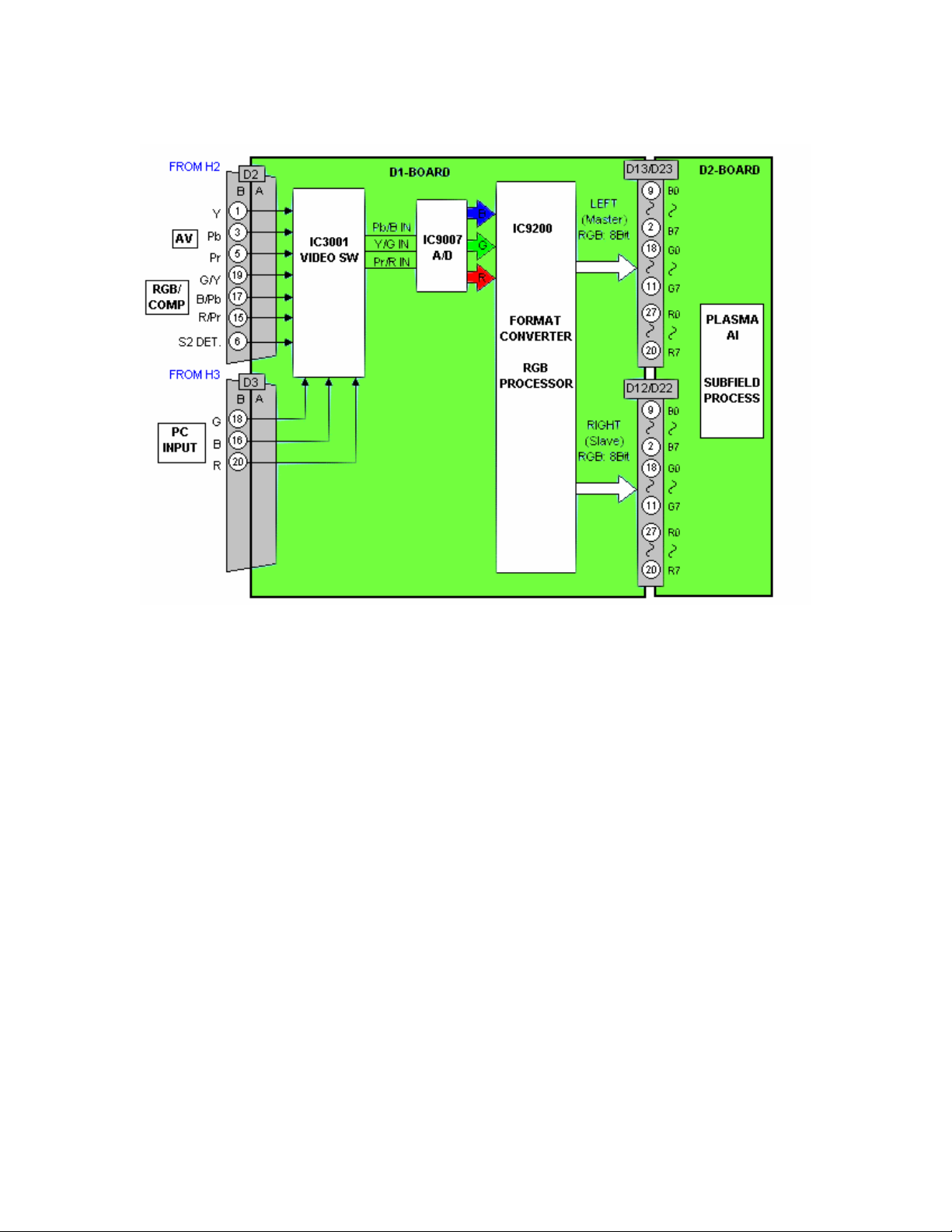
D1 Board
Figure 20
D1-board consists of the Analog and Digital signal process. It also contains the
Discharge control and Microprocessor control block. Supply voltages of 13.5V,
5V, Standby 5V, 3.3V, and 1.8 V operate the D1-board. The input RGB video
signals are at 0.7Vp-p. Video signals in the form of parallel data and the control
signals for the data drive circuit are output.
D1 Main ICs Operation
IC3001 Video Switch
The user selects the desired video input using the front panel button or the
remote control. The microprocessor reads this data and sends out a command
via the IIC bus line. The IIC data is read by IC3001 and the video input is chosen.
IC9007 A/D Converter
This integrated circuit converts the RGB analog signals to eight bit parallel data.
IC9200 Format Converter
The digital video data is converted to progressive scan and mixed with the OSD
data. Other adjustments such as white balance, contrast and color are also
corrected here. The two channels of data are output to the D2 board for the subfield drive circuit.
22
Page 22
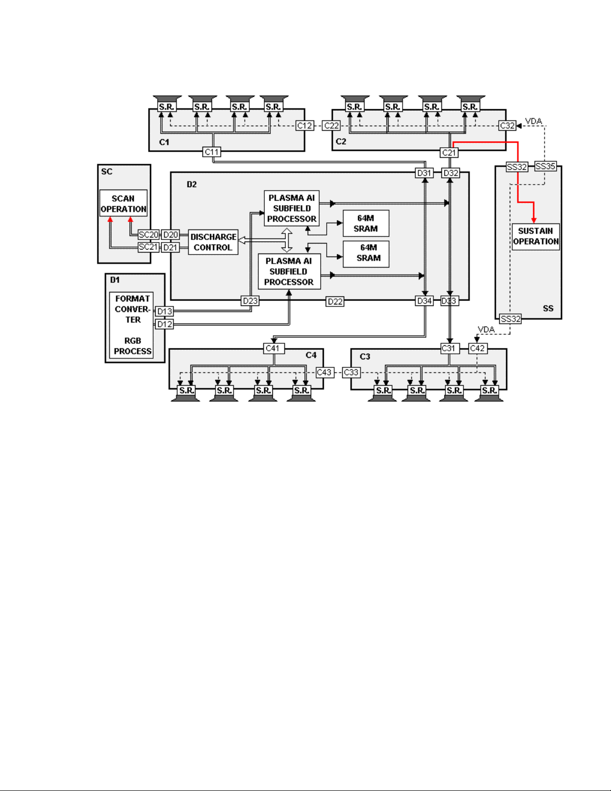
D2 Board
Figure 21
The D2 board provides the scan, sustain and data drive signals. The scan pulses
are output to the SC board. The sustain pulses are output to the SS board. The
data drive signals are output to the C1, C2, C3 and C4 boards. The C1 board
drives the Upper right portion of the panel; the C2 board drives the upper left
portion. The C3 and C4 boards drive the lower right and left portions of the panel
respectively.
23
Page 23
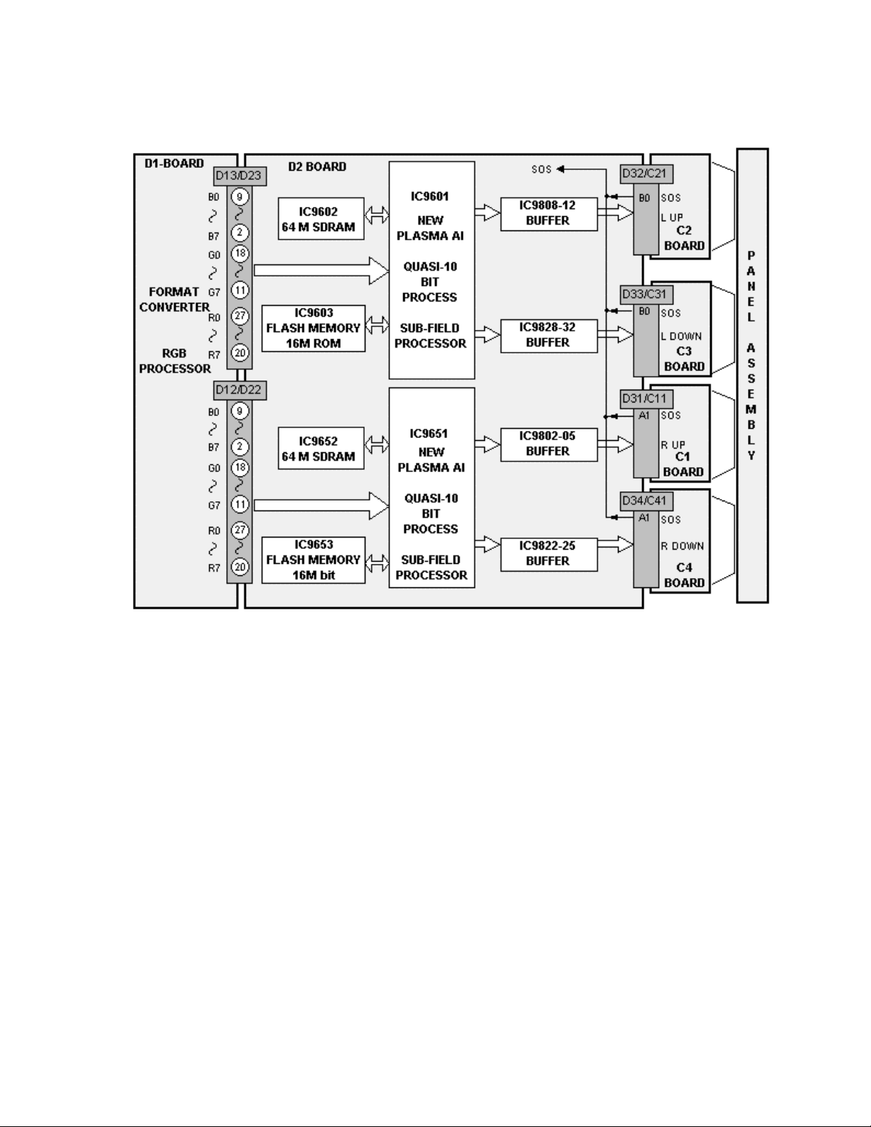
D2 Board details
Figure 22
The Plasma AI (Adaptive brightness Intensifier) circuits analyze the video
program level for the distribution of dark and bright components. The upper and
lower eight bit video signals are memorized into two Plasma AI processors
IC9651 and IC9601. The Plasma AI circuits converts the 8 bit signal data to 10
bit signal data. The Flash memories contain the algorithms for the AI circuit. Two
AI processors are used to speed up the scanning process and control the
number of sustain periods. This increases the brightness and improves the
contrast ratio.
24
Page 24
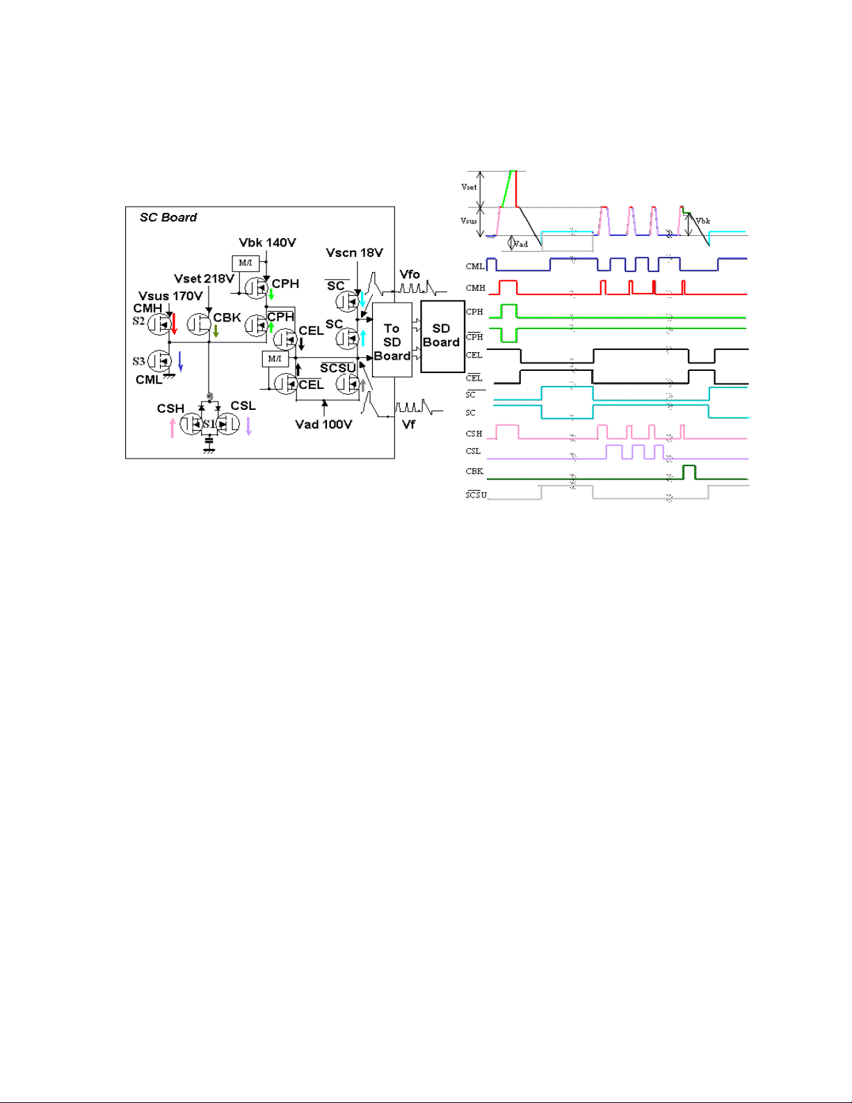
SC Board Explanation
Figure 23
25
Page 25
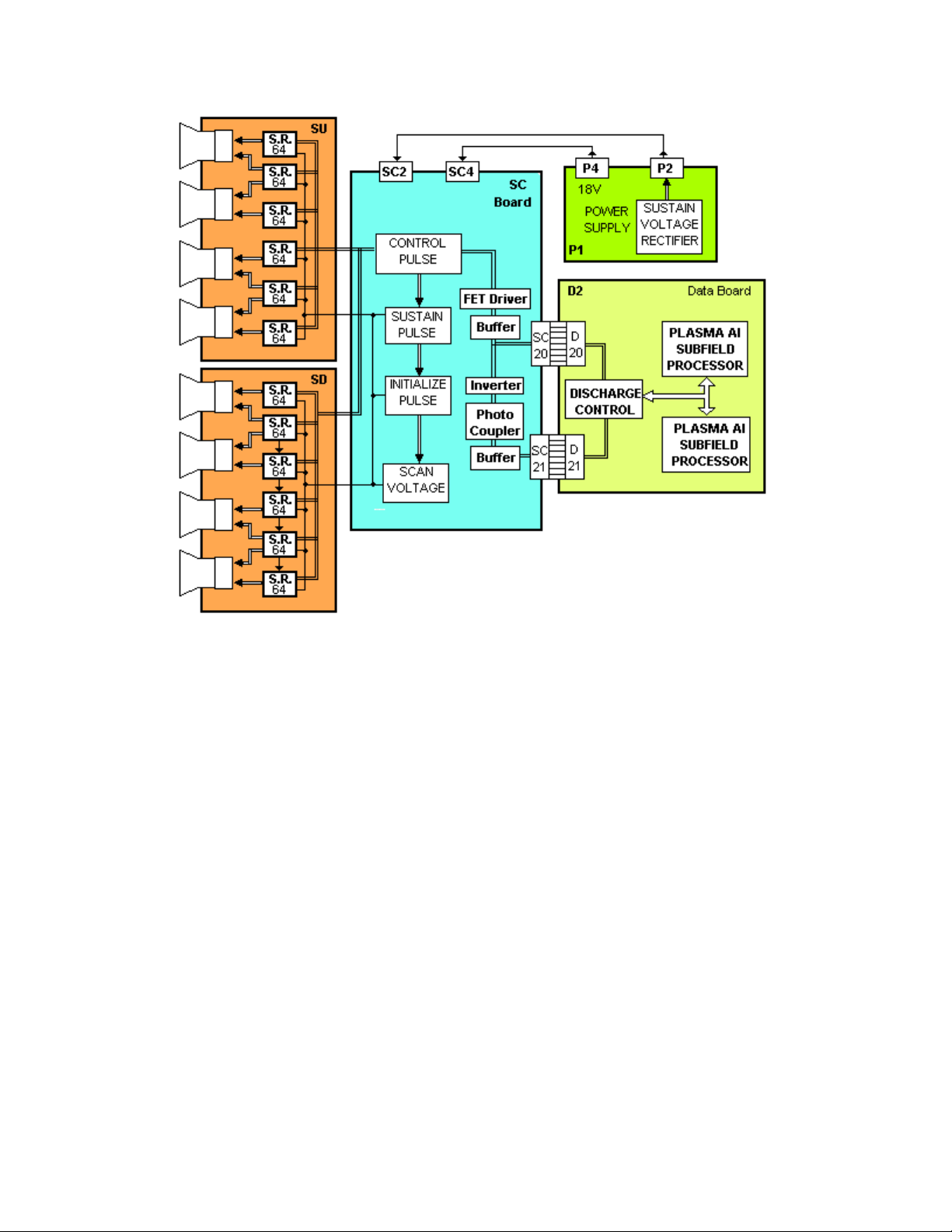
Figure 24
The SC Board consists of buffers and drivers used to generate the scan signals
to the panel. The buffers provide isolation between the D2 board and the drivers.
Connector SC20 provides the drive signals (140V, 100V and 18V). Connector
SC21 provides trigger signals to switch the FET transistors. The D2 board
switches the FETs on and off to create the distinctive scan signal. Each trigger
signal switches a drive FET creating a portion of the waveform. For example,
applying the CPH signal to the 140V FET creates the peak portion of the
waveform, see figure 23.
26
Page 26
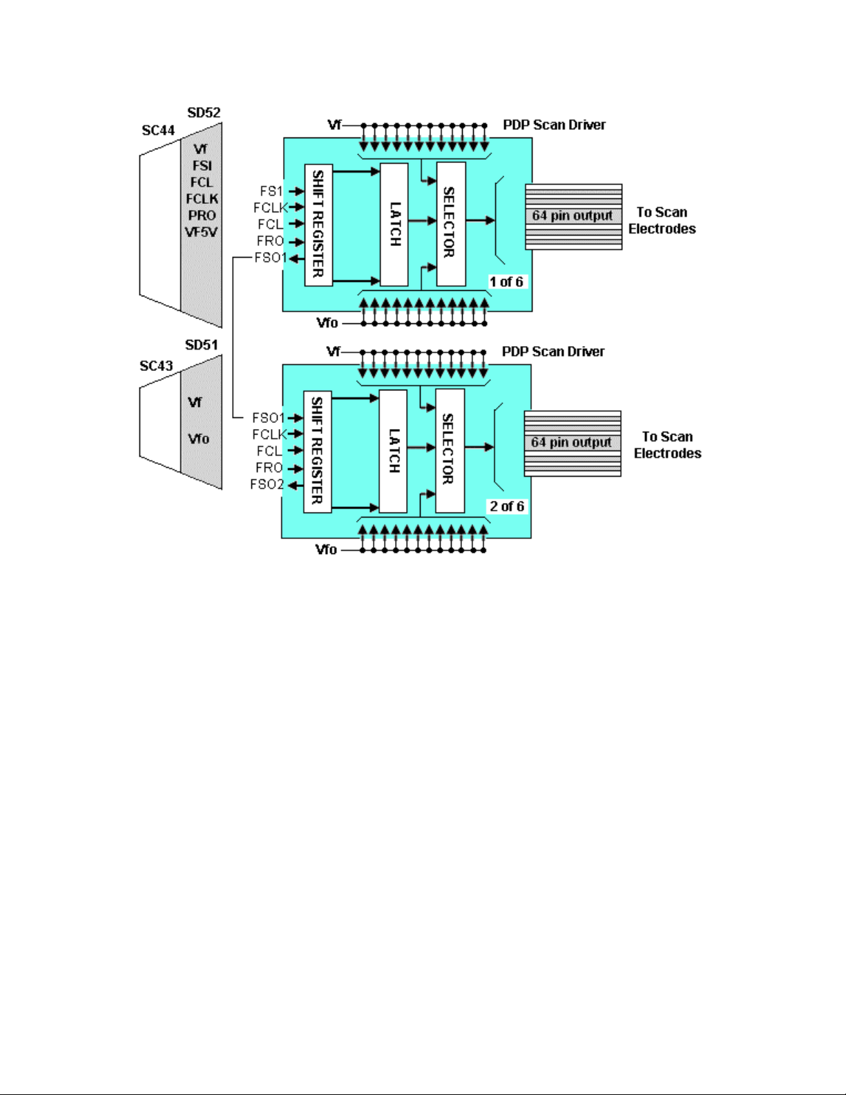
Figure 25
After the scan waveform is developed on the SC Board, it is applied to the SU
and SD boards for de-multiplexing. The signal is input to a series of shift registers
inside the PDP scan driver IC. Figure 25 shows an example of the demultiplexing circuit. There are six driver ICs on the SU board and six on the SD
board.
27
Page 27
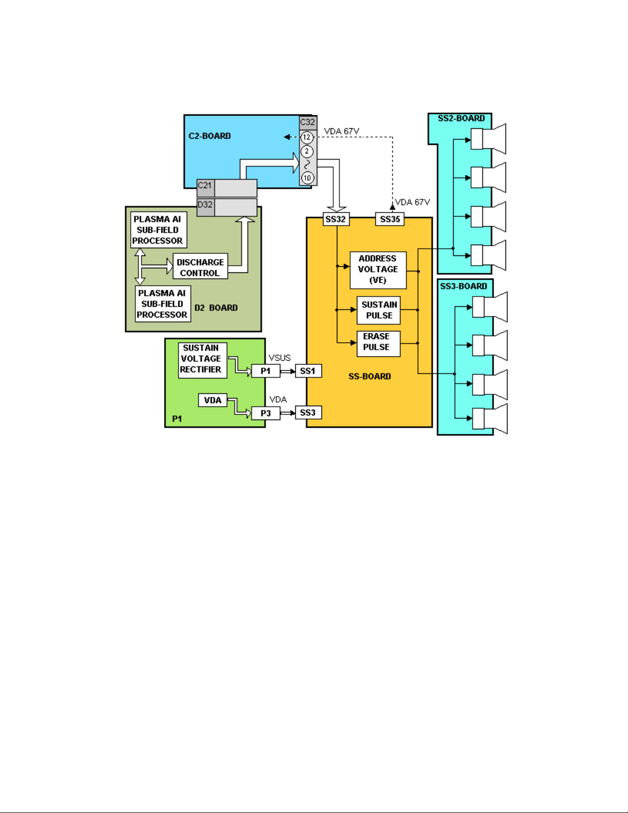
SS Board Explanation
Figure 26
After the video signal is processed on the D2 board, the sustain and erase pulses
are output to the SS board. The erase pulse is output at the beginning of each
scan period. The pulse is applied to the SS2 and SS3 boards to remove the
previous charge for the upper and lower sections of the display panel.
The sustain pulses are also developed on the D2 board and are applied after the
scan periods.
28
Page 28
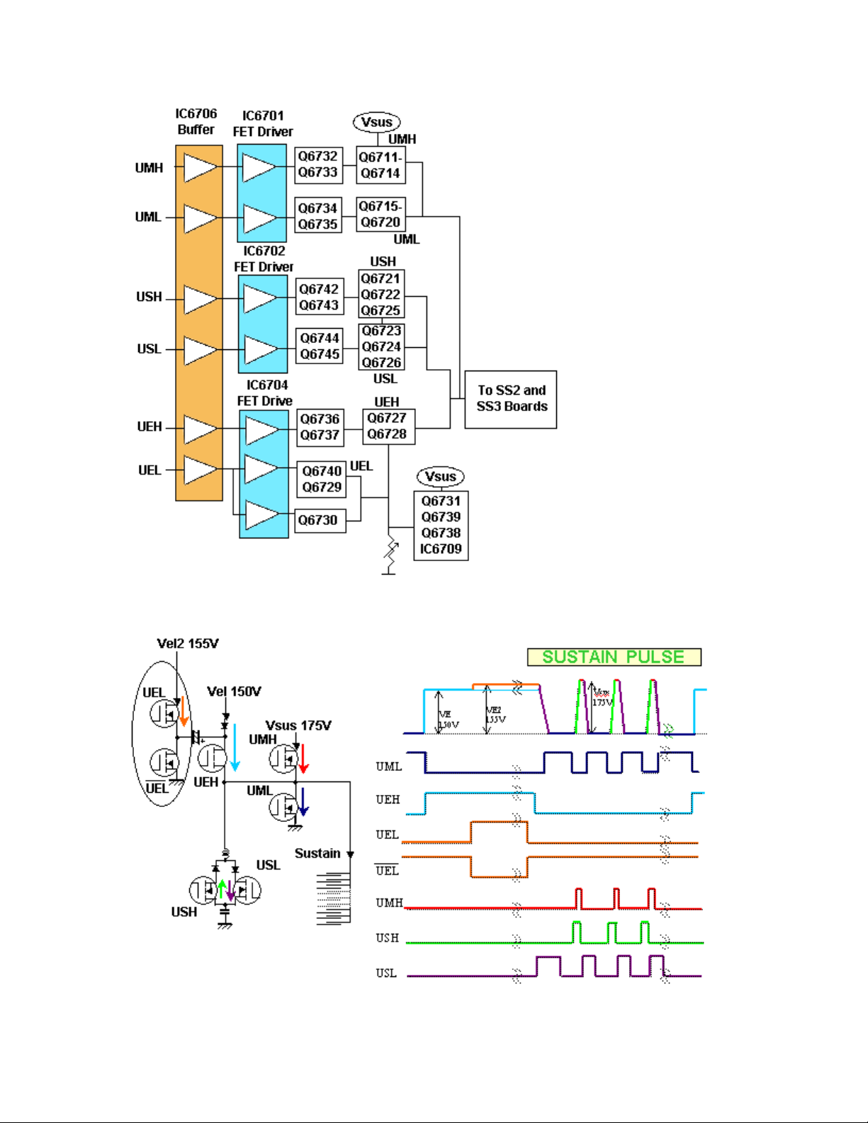
Figure 27
Figure 28
29
Page 29

The Sustain pulse is developed using a similar circuit as the Scan Pulse. A series
of specifically timed pulses are applied to FET drivers creating the distinctive
sustain pulse. The drivers switch the voltages (150V, 155V and 175V) at selected
intervals determined by the D2 board. The basic waveform remains constant but
the exact number of sustain pulses is determined by the amount of luminance
required, see figure 28.
30
Page 30

Power Supplies
Standby Power Supply
Figure 29
The standby power supply provides the necessary DC voltage for the system
control Microprocessor, Reset circuit and the EEPROM. D421 rectifies the
incoming AC Voltage and applies it to the transformer T402 and the standby B+
control circuit IC400. The output pulses of IC400 are then applied to the primary
side of transformer T402. Diode D439 rectifies the AC output at pin 15 of the
secondary of T402 to create STB (Standby) voltage for the system control circuit.
The AC output at pin 14 of the secondary of T402 is rectified by diode D440 to
create the DC voltage for the power relays. Transistor Q418 creates the ground
path for power relay RL401. Transistor Q417 provides the ground path for the In
Rush Current relay RL400. The Opto-coupler D431 provides feedback to the
STB control circuit for voltage regulation.
31
Page 31

Main Power Supply
Figure 30
Power Factor Control
The power factor control circuit operates like a boost regulator. The incoming AC
voltage, after being switched on, enters the rectifier D402 where it is converted to
DC. The Power Factor Control (PFC) circuit converts the DC level to 400Vdc.
The negative side of the bridge rectifier D402 connects to ground via a resistor.
As current flows through the resistor, the resulting voltage drop enters pin 5 of
connector P19/P19A of the power factor control circuit board. The power factor
control circuit board is a switching control oscillator circuit which boosts the input
voltage at pin 2 of the transformer T401 to 400Vdc. As the pulses are output at
pin 4 of connector P19/P19A, the transistors Q400~Q405 are switched On/Off
controlling the charge and discharge time of the inductor L401. The output
voltage is monitored via pin 11 of the connector P19/P19A. The resistor R548
adjusts the output voltage to 400Vdc. The 400Vdc output to pin 2 of the
transformer T401 subsequently enters the drain of transistor Q416.
32
Page 32

Low Voltage Power supply
VCC and Start-up voltage for the low voltage power supply is provided to IC650
of the P5 Board by the standby power supply circuit (not shown). Upon start-up
of the switching control circuit, a pulse width modulated signal is output at pin 9
of connector P18/P18A to drive the switching transistor Q416. When Q416 is on,
current flows via the primary winding of transformer T401 and Q416. As current
flows through the transformer, energy is built up and stored in the transformer.
When Q416 turns off, the energy within the transformer begins to collapse. As
the field collapses, energy is released in the windings of the transformer to
provide the secondary voltages.
The rectified AC output at pin 10 of transformer T401 is applied to IC401 where it
is regulated to 18V. This voltage is used to power the Drive Oscillator circuit
board that will be discussed later.
Voltage Regulation
The 13.5V source and the VDA source voltage levels are monitored by IC650 of
the P5 Board. A voltage increase of the 13.5V or an increase in the current flow
of the VDA source causes IC416 to conduct harder, allowing more current to flow
through the LED inside opto-coupler D432. This increases the conduction of the
transistor inside D432. Conversely, a decrease in the 13.5V supply voltage or a
decrease in the current flow of the Vda source decreases the conduction of
IC416. Any change in the conduction of IC416 is monitored by pin 10 of IC450.
As a result, the pulse width modulated output at pin 10 of IC650 adjusts to keep
the output level of the power supply constant. R545 is used to adjust Vda to the
proper voltage level.
33
Page 33

High Voltage Power Supply
Figure 31
The P3-Board contains the drive voltage oscillator circuit that develops the Vsus
voltage needed to drive the Scan and Sustain boards. Operation begins with the
18Vdc supply being applied to pin 12 of connector P15. This voltage serves as
start up voltage for IC601. Q604, connected to pin 7 and 9 of the IC, provides
Oscillation control. The oscillator generates a trapezoid pulse that is input to a
PWM circuit (not shown) to control the output voltage. The PWM output at pin 2
of IC601 is applied to pin 2 and 3 of IC600. This IC is a wave driver that provides
two square wave outputs at opposite polarity. The two signals are then output to
the P1 board as H OUT at pin 1 and L OUT at pin 6 of connector P15.
Amplification of the two signals is performed the transistors Q407, Q408, Q409,
Q410 before being applied to the transformer T400. The output of the
transformer is provided to the SC-Board via pin 1 and 2 of the connector P2 and
to the SS board via Pins 2 and 3 of the connector P1.
Voltage feedback is provided via pin 8 of connector P16. This voltage enters pin
5 of IC601 for voltage regulation. R625 is used to set the output at the desired
level.
Note: The voltage level of the Vsus output is not mentioned because it is
different for each plasma display panel. This voltage level can be found on the
panel information label located on the heat sink of the panel.
34
Page 34

Over-voltage protection (OVP) is provided via pin 6 of connector P16. This
voltage enters pin 4 of IC601 for immediate shutdown of the IC if the Vsus
voltage rises to an undesired level. The OVP feedback is also provided to the
system control circuit via pin 13 of connector P15 for immediate shutdown of the
entire unit.
The P7 (High Voltage Protector) and P8 (Low Voltage Protector) circuit boards
monitor the DC output of all power supply boards. If any of the inputs is higher
than the desired level, a DC level is output via the “SOS IN” line to pin 1 of
connector P16. The operation is the same as the OVP input at pin 6 of the
connector P16.
35
Page 35

Protection Circuits
Figure 32
Protection circuits are incorporated in the unit to prevent the failure of a single
circuit or component from creating catastrophic damage.
The P7 and P8 boards are daughter boards on the P1 main power supply board.
The P7 board monitors the Vbk (195V), Vda (75V) and +17V supply voltages.
The voltages are fed through individual voltage dividers and the result is
compared to a 3.3V reference voltage by a comparator IC750. If any of the
voltages drop low, the comparator outputs a low triggering Q751. Q751 triggers
Q750 on, applying a high to pin 95 of the main CPU IC9351.
The circuitry on the P8 board monitors the plus and minus 13.5V lines used by
the audio circuit, the +5V line and another +13.5V line. If any of these supplies
were to drop, the comparator will output a low signal turning on Q776. Q776
conducts applying a high to pin 95 of the main CPU IC9351.
The four ventilation fans are monitored to be sure they are operating properly. If
one of the fans opens or increases resistance, the resulting current change is
applied to pin 98 of the main CPU.
The Scan and Sustain voltages on the SC and SS boards are monitored in a
similar manner. The +15V Line on the SS board is fed to a voltage divider and
36
Page 36

the result is compared to a reference voltage. The reference voltage is provided
by a zener diode. If the output of the comparator goes high, Q6741 turns on
effectively grounding the SOS line. The SC board uses a similar circuit to monitor
the +17V line.
The SS and SC boards contain an LED indicator to alert the technician when a
problem exists. The LED should be lit during normal operation, a dark LED
indicates that a problem exists on that board.
37
Page 37

Diagnostic Procedures
Self Check Display Indication
Self-check is used to automatically check
the bus line controlled circuits of the
Plasma display.
To get into the Self-check mode, press
and hold the Volume Down button on the
front of the unit, then the OFF-TIMER
button on the remote control. The graphic
in figure 32 should be displayed.
Note:
In case the H, HY or HZ boards are
disconnected, “IC3699 - -” is displayed.
Figure 33
38
Page 38

Power LED Flashing timing chart
When an abnormality has occurred in the unit, the protection circuit operates and
shuts off the power supply. The faulty area can be identified by the number of
flashes of the Power LED at the front of the unit.
39
Page 39

Diagnostic Flow Charts
No
P-Board.
Replace the defective
Yes
power LED
No
Yes
No Power
There are three states of “No Power” indication by the power LED:
1. The power LED does not light up.
2. The power LED is green at power up. It then turns red a few seconds later
and blinks on and off.
3. The power LED is red at power up and never changes state.
The F Board is suspected to be
Does the
turn on?
Check the
Do F900
and F901
measure
correctly?
component.
defective.
40
Page 40

The Power LED is red and blinking on/off.
Remove Connector P5
Check the output of the
Is the Power LED still
When one or more of the power supply voltages is missing, the red LED blinks
on and off.
Blinking stops
But still no picture
Yes
Is the LED still
blinking red?
No
Check D1-Board.
P-Board.
No
Remove Connector P1, P2.
blinking red?
Yes
Check SS/SC-Boards.
41
Page 41

Power LED blinks twice
Is the SC board
LED lit?
to be defective.
suspected to be defective.
NO
Are the SS board
LEDs lit?
Is the Vda voltage
correct?
The D1 is suspected to be
defective.
YES
YES
YES
NO
The SS board is suspected to
be defective.
NO
The SC board is suspected
The Power supply is
42
Page 42

No Picture Flowchart 1
problem exist on
all inputs?
problem exist on
Is the On screen
Display information
Yes
Does the
Yes
No
Is the SC
Board LED
illuminated?
No
SC Board is probably
defective.
No
Yes
Is the SS
Board LED
illuminated?
No
SS Board is
probably defective.
Yes
D1 or D2 Board
is probably
defective.
Does the
Composite
Yes
HZ Board is
probably defective
43
No
Does the
problem exist
on PC/RGB
Yes
HX Board is
probably defective
Page 43

No picture Flowchart 2
Are the video signals
Is the SC board
LED lit?
to be defective.
The D2 Board is suspected to
be defective.
connectors SC2 and SC23
of the SC board correct?
The Power Supply is suspected
connectors SC20 and SC21
The D2 Board is suspected to
be defective.
to be defective.
NO NO NO NO
correct at the D1
board input?
Is the TPSC1
Waveform incorrect?
Are the voltages at
Are the trigger signals at
of the SC board correct?
The SC Board is suspected
NO
Reference the HY/HZ and HX
board troubleshooting charts
YES
The SC board is suspected
YES
YES
to be defective.
YES
YES
44
Page 44

Dark picture Flowchart
Are the video signals
board LEDs lit?
to be defective.
The D2 Board is suspected to
be defective.
Are the voltages at connectors
board correct?
The Power Supply is suspected
The D2 Board is suspected to
be defective.
to be defective.
NO NO NO NO NO
correct at the D1
board input?
Are the SS
Is the TPSS1
Waveform incorrect?
SS11 and SS12 of the SS
Are the trigger signals at
connector SS33 of the SS
board correct?
The SS Board is suspected
YES
YES
YES
YES
YES
Reference the HY/HZ and HX
board troubleshooting charts
The SS board is suspected
to be defective.
45
Page 45

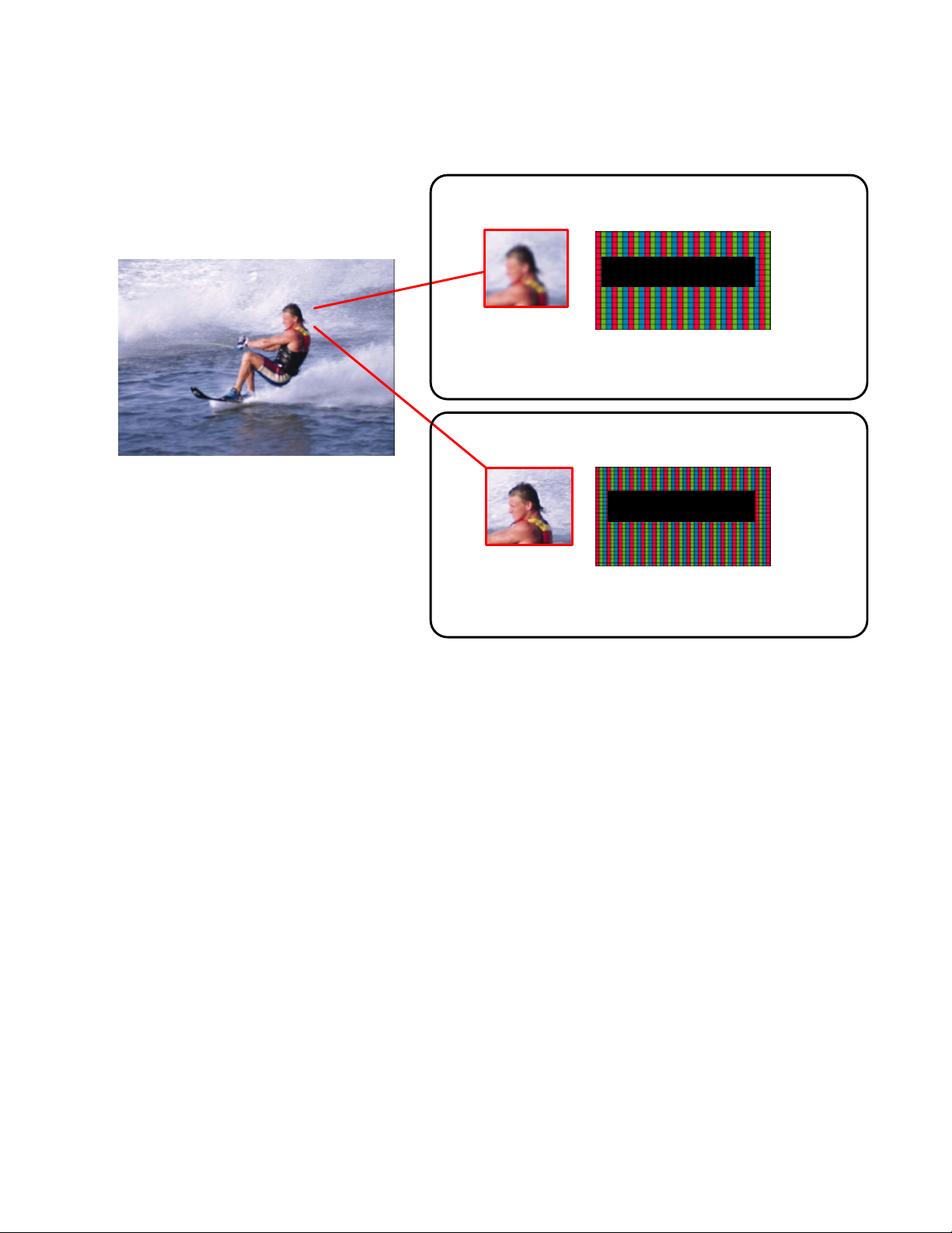
Local screen failure
The Plasma Display Panel unit may develop a failure, where the symptom is
localized in a particular area of the screen. The figure below can help localize the
circuit board that is most likely to be defective. In the example in figure 34, one
of the two boards, C3 and D2 is likely to be the cause.
Figure 34
Service Hints
Symptom: No picture (black Screen)
v Suggestion: The use of a magnifying glass can help localize the defective
printed circuit board. Use the
magnifying glass to take a close
look at the pixels of the screen.
1. If the pixels are totally dark, the
defect is most likely located in
one of the following boards:
a) SC-Board
b) SU-Board
c) SD-Board
1. Check the status of the LED located on the SC-Board; if the LED is dark, a
malfunction of the SC-Board is suspected.
Figure 35
46
Page 46

2. Listen to the buzz noise of the SC board; if the buzz noise is not present, a
malfunction of the SC-Board is suspected.
Figure 36
Suggestions: Check the Scan pulse waveform at
TPSC1. (Use TPSS1 of the SS-board to trigger
the oscilloscope.)
Verify the input signals at connector SC2, SC4,
SC20 and SC21.
Verify that the signals of the clock and serial data
lines from the D-board are present at connector
SC20 and SC21.
Figure 37
47
Page 47

Symptom: No picture (black Screen)
Figure 38
v Suggestion: The use of a magnifying
glass can help localize the defective
printed circuit board. Use the magnifying
glass to take a close look at the pixels of
the screen.
If the pixels are faintly lit, the defect is
most likely located in one of the following
boards:
A) SS-Board
B) SS2-Board
C) S3-Board
1. Check the status of the LED located on the SS-Board; if the LED is dark, a
malfunction of the SS-Board is suspected.
2. Listen to the buzz noise of the SS-board. If the buzz noise is not present,
a malfunction of the SS-Board is suspected.
3. Verify the input signals at connector SS3 and SS1.
SS Board
Figure 39
48
Page 48

Suggestions: Check the
Scan pulse waveform at
TPSC1 of the SC-Board.
(Use TPSS1 of the SSboard to trigger the
oscilloscope.) Proceed to
check the power sources at
connector SS11, SS12 and
SS33.
Verify that the clock and
serial data lines from the Dboard are present at
connector SS33.
Note: It is easier to
measure input levels at
connector C33 of the C3Board instead of connector SS33.
Figure 40
49
Page 49

Symptom: Horizontal Black Bar
(Completely dark)
Note: The use of a magnifying glass can help
localize the defective printed circuit board. Use
the magnifying glass to take a close look at the
pixels in the area of the black bar.
1 If the pixels are totally dark, the defect is
most likely located in one of the following
boards:
a) SC Board
b) SU Board (upper half of the screen only)
c) SD Board (lower half of the screen only)
2. If the pixels are dimly lit, the defect is most likely located in one of the
following boards:
a) SS Board
b) SS2 Board (upper half of the screen only)
c) SS3 Board (lower half of the screen only)
Figure 41
50
Page 50

Symptom: Vertical Black Bar
• Suggestion: Since the C2 board
contains the serial to parallel
converters for the picture data that
drive this portion of the screen; the
most likely cause for this defect can
be localized to the C2-Board or the
D2-Board.
q Symptom: Vertical Black Bar
Suggestion: Since the C3 board
contains the serial to parallel
converters for the picture data that
drive this portion of the screen; the
most likely cause for this defect can
be localized to the C3-Board or the
D2-Board.
Symptom: No OSD but it has video.
v Suggestion: Check signal on the D1 board.
Figure 42
Figure 43
51
Page 51

v Symptom: Burned image
Panasonic
(pattern) is visible.
Suggestion: Activate the scroll
bar or run the set with a white
raster for at least fifteen minutes.
Figure 44
52
Page 52

After Image Prevention
Figure
45
If a customer has been viewing a 4:3 picture or another stationary pattern for a
long period of time it is possible for an after image to be burned into the panel.
Advise the customer that operation in 4:3 mode for a long period can cause a
permanent image burn, damaging the panel. Use of Just mode or Full mode is
recommended if the input video source is 4:3 aspect ratio. Pressing the Aspect
button on the remote control selects Just or Full mode.
Screen Saver Feature
The Screensaver feature may repair after image damage.
1. Press the Setup button on the remote control.
2. Use the Up/Down arrow buttons on the remote to highlight screensaver,
then press the center button.
Figure 46
Figure 47
Use the Up/Down arrow buttons to highlight
the function. Use the Left/Right Arrow buttons
to change the setting.
Negative causes the image to invert, white areas become dark and vice
versa. White bar scroll causes a white bar to appear and scroll across the
screen continuously. Select White bar scroll, then use the arrow down
button and then change the mode to ON.
3. Once the mode is ON the menu will
disappear and the scrolling bar will appear.
Let the Scrolling bar screensaver run for at
least 15 minutes if you are attempting to
remove an after image problem.
53
Figure 48
Figure 49
Page 53

4. To stop the screen saver, press the R button on the
remote control.
Side Bar Brightness adjustment
This feature allows the customer to adjust the
brightness of the non-picture area on either side
of the 4:3 image on screen.
1. Press the Setup button on the remote control.
2. Use the Up/Down arrow buttons to highlight Side bar adjust, then press
the action button.
3. Use the Left/Right Arrow buttons to select the desired setting, Off ? Dark
Note: Setting the side bar to Bright may cause a flashing effect depending on
the image being displayed. Also Bright sidebars may cause an after image.
4. Press the R button on the remote control to exit this
Figure 54
? Mid ? Bright.
menu.
Figure 51
Figure 52
Figure 53
Figure 55
Figure 50
54
Page 54

Option Setting
Accessing the Option Menu
1. Press to display the Setup
menu.
2. Press to select OSD Language.
3. Press the surround button on remote control for
more than three seconds. The action menu
should be displayed on screen.
Figure 56
Figure 57
55
Figure 58
Page 55

Settings the Action Menu
1. Use the Up/Down buttons to select the desired
item.
2. Use the Left / Right Buttons to select the
desired function
Figure 59
The option menu will disappear 60 seconds after
the operation.
Press the R button to exit the Option Menu.
Figure 60
Hidden Option Menu for GPH5D series
GPH5D chassis series have special function and operation setting facility that is
called “Option Menu”. This Option Menu is useful for special functions that are
required by certain customers. This should be set at the installation stage. The
end user could not set or change these because the optional On Screen menu is
hidden and accessible via the CAT-mode only.
Option menus Default setting Contents
Wobbling Off Wobbling operation On/Off.
The outline of burnt image will be blurred by
intermittent image shift.
Off-timer function Enable Off-timer operation Enable/Disable.
On Screen display Off Enable/Disable to display input mode
indication after power on and no signal
indication.
Input Initial Off Sets the initial input mode when the power is
turned on. Allow input mode selection while
power is on.
Initial VOL. level Sets the initial volume level when the power is
turned on. Allow Volume control while power
is on.
Maximum VOL. Level Off Sets the maximum volume to desired level.
Volume cannot exceed this level.
INPUT lock Off Fixes the input mode to AV, Component/RGB
or PC. Cannot change input mode by input
selection key.
Button lock Off Enable/Disable front operation buttons (Input
and/or volume up/down)
Studio W/B Off Set warm mode color temperature to 3,200
Kelvin.
Remote control User
Level
Off Remote key invalidation
Off: All keys of the remote are valid.
User1: The keys that are Valid are: Stand-by
(ON/OFF), Input, Status, Surround, Sound
mute On/Off, and volume adjustment.
User2: The key that is Valid is only the Stand-
by (ON/OFF).
56
Page 56

Note:
Setting the remote control User Level and Remote ID off.
1. Access service mode (CAT-mode) and press SET UP key on remote.
2. Access the hidden option menu.
3. Change the remote control User Level and/ or Remote ID set to off.
57
Page 57

Sample Waveforms
VIDEO/YUV
HY/HZ board
The pages that follow contain samples of waveforms that are present when the
unit is in good operating condition. Prior to determining that a board should be
replaced, it is advisable that these waveforms are checked to help achieve the
right conclusion.
CONVERTER
Figure 61
Figure 61 is an illustration of the HZ-Board. The board is the interface between
the AV inputs and the D1-Board. When troubleshooting, connect a signal source
to the input terminals and observe the output signals at the connector.
58
Page 58

Vertical Output
The waveforms listed below must be checked at connector H2 of the HZ-
CN H2, Pin B1
20us/div., 20mV
Green Signal Output
CN H2, Pin A6
20us / div., 0.2V
Horizontal Output
CN H2, Pin A20
0.1ms/div, 0.2V
SDA3
Board.
CN H2, Pin B3
20us/div., 20mV
Blue Signal Output
CN H2, Pin A8
5ms /div., 0.2V
CN H2, Pin B5
20us/div., 20mV
Red Signal Output
CN H2, Pin A19
0.1ms/ div., 0.2V
SCL3
Note: If any of the signals shown here is missing, this
indicates a possible malfunction of the HZ-Board. Verify
that all DC and I2C inputs to the HZ-Board are present. If
these are correct, replacement of the HZ-Board is
recommended.
59
Page 59

SCL3
SDA3
The waveforms listed below must be checked at connector H2 of the HZ-
Board.
CN H2, Pin B19
5us/div 20mV
Green Signal Input
CN H2, Pin A19
0.1ms/div, 0.2V
Note: A possible malfunction of the HZ-Board may exist if any of the signals
listed above is missing. Verify that all DC and I2C inputs to the HZ-Board
are present.
If these are correct, replacement of the HZ-Board is recommended.
CN H2, Pin B17
5us /div, 20mV
Blue Signal input
CN H2, Pin B15
5us /div, 20mV
Red Signal Input
CN H2, Pin A20
0.1ms/ div, 0.2V
60
Page 60

HX board
Figure 62
Figure 62 is an illustration of the HX-Board. The board is the interface between
the PC input and the D1-Board. When troubleshooting, connect a PC to the input
terminals and observe the output signals at connector HX1/D3. See the next
page for waveform samples.
61
Page 61

Note: The signals listed below must be checked at connector HX1 of the HXBoard.
CN HX1, Pin B20
10us / div.20mV
Red Signal Input
CN HX1, Pin B18
10us_20mV
Green Signal Input
CN HX1, Pin B16
10us/ div, 20mV
Blue Signal Input
CN HX1, Pin B12
5ms/ div, 0.2V
Vertical Drive
CN HX1, Pin B14
10us/div, 0.2V
Horizontal Drive
CN HX1, Pin A4
5us/ div, 20mV
Serial Data
Note: A possible malfunction of the HX-Board may
exist if any of the signals listed on this page is missing.
Verify that all DC inputs to the HX-Board are present. If
these are correct, replacement of the HX-Board is
recommended.
CN HX1, Pin B4
5ms/ div, 0.2V
Serial Clock
62
Page 62

SC Board Input Signals
Figure 63
Figure 63 is an illustration of the SC-Board connection to the remaining boards of
the panel. The SC-board is the interface between the D2-Board, SU and the SD
Boards. When troubleshooting, connect a fixed video source to any of the input
terminals and observe the input signals at connector SS20 and SS21. See the
next two pages for waveform samples.
63
Page 63

SC Board Waveforms
The waveforms listed below must be checked at connector SC20 of the SCBoard.
CN SC20, Pin 1
1ms / div, 0.2V
CRL
CN SC20, Pin 6
1ms / div, 0.2V
CSL
CN SC20, Pin 9
1ms / div, 0.2V
CMH
CN SC20, Pin 2
1ms / div, 0.2V
CEL
CN SC20, Pin 7
1ms / div, 0.2V
CSH
CN SC20, Pin 10
1ms / div, 0.2V
CRH
CN SC20, Pin 3
1ms / div, 0.2V
CEH
CN SC20, Pin 8
1ms / div, 0.2V
CML
64
Page 64

The waveforms listed below must be checked at connector SC21 of the SCBoard.
CN SC21, Pin 2
1ms / div, 0.2V
CL
CN SC21, Pin 3
1ms / div, 0.2V
CLK
CN SC21, Pin 4
1ms / div, 0.2V
SIU
CN SC21, Pin 6
1ms / div, 0.2V
SID
CN SC21, Pin 7
1ms / div, 0.2V
SCSU
CN SC21, Pin 8
1ms / div, 0.2V
CPL
CN SC21, Pin 9
1ms / div, 0.2V
CPH
65
Page 65

SS-Board Input Signals
Figure 64
Figure 64 is an illustration of the SS-Board connection to the remaining boards of
the panel. The SS-board is the interface between the D2-Board, SS2 and the
SS3 Boards. When troubleshooting, connect a fixed video source to any of the
input terminals and observe the input signals at connector SS32. See the next
page for waveform samples.
66
Page 66

SS Board Waveforms
The waveforms listed below must be checked at connector SS32 of the SSBoard.
CN SS32, Pin 2
1ms / div, 0.2V
URH
CN SS32, Pin 5
1ms / div, 0.2V
UBL
CN SS32, Pin 8
1ms / div, 0.2V
UMH
CN SS32, Pin 3
1ms / div, 0.2V
UEL
CN SS32, Pin 6
1ms / div, 0.2V
USH
CN SS32, Pin 10
1ms / div, 0.2V
URL
CN SS32, Pin 4
1ms / div, 0.2V
UEH
CN SS32, Pin 7
1ms / div, 0.2V
UML
67
Page 67

Zone B
25%
PDP Defect Pixel Specification
1. Dead Pixel (pixel is always off)
2. Lit Pixel (pixel is always
3. Pair defect (Adjacent pixels
4. Defects Distance (Distance between
nearest two defective pixels)
Check Zone
Zone A
25%
Specification
Lit Pixel
Single Defect Pair Defect Defect Distance
G 0
A R 0 0 -
B 3
G
B R 0 6 0 5 cm
B
68
Dead PixelZone
Page 68

Connector Tables
F-BOARD CONNECTORS
The following table lists the voltage levels present at each pin of the connectors
of the F-Board. Use this information to confirm that the F-Board is operating
properly.
Connector F1
Pin Numbers
1 AC IN AC Line Input Level
2 NC
3 NC
4 NC
5 AC IN AC Line input Level
Connector F9
Pin Numbers
1 AC OUT AC Line input Level
2 NC
3 NC
4 NC
5 AC OUT AC Line input Level
P-BOARD CONNECTORS
The following table lists the voltage levels present at each pin of the connectors
of the P1-Board. Use this information to confirm that the P1-Board is operating
properly.
Connector P1/SS1
Pin Numbers
1 NC P1---àSS1 (SS-BOARD)
2 VSUS P1---àSS1 (SS-BOARD)
3 VSUS P1---àSS1 (SS-BOARD)
4 NC P1---àSS1 (SS-BOARD)
5 GNDa P1---àSS1 (SS-BOARD)
6 GNDa P1---àSS1 (SS-BOARD)
7 GNDa P1---àSS1 (SS-BOARD)
Connector P2/SC2
Pin Numbers
1 VSUS P2---àSC2 (SC-BOARD)
2 VSUS P2---àSC2 (SC-BOARD)
3 NC P2---àSC2 (SC-BOARD)
4 GNDa P2---àSC2 (SC-BOARD)
5 GNDa P2---àSC2 (SC-BOARD)
6 GNDa P2---àSC2 (SC-BOARD)
Signal Name Voltage Findings
Signal Name Voltage Findings
Signal Name Signal Flow
(Board or Connector)
Signal Name Signal Flow
(Board or Connector)
69
Page 69

P-BOARD CONNECTORS (Continued)
Connector P3/SS3
Pin Numbers
1 VDA P3---àSS3 (SS-BOARD)
2 VDA P3---àSS3 (SS-BOARD)
3 NC P3---àSS3 (SS-BOARD)
4 +17V P3---àSS3 (SS-BOARD)
5 GNDa P3---àSS3 (SS-BOARD)
6 GNDa P3---àSS3 (SS-BOARD)
7 GNDa P3---àSS3 (SS-BOARD)
8 GND P3---àSS3 (SS-BOARD)
9 NC P3---àSS3 (SS-BOARD)
10 STB PS P3---àSS3 (SS-BOARD)
Connector P4/SC4
Pin Numbers
1 +17V P4---àSC4 (SC-BOARD)
2 +17V P4---àSC4 (SC-BOARD)
3 GNDa P4---àSC4 (SC-BOARD)
Connector P5/D25
Pin Numbers
1 13.5V P5---àD25 (D2-BOARD)
2 13.5V P5---àD25 (D2-BOARD)
3 GND P5---àD25 (D2-BOARD)
4 GND P5---àD25 (D2-BOARD)
5 +5.2V P5---àD25 (D2-BOARD)
6 GND P5---àD25 (D2-BOARD)
7 FAN CONT P5---àD25 (D2-BOARD)
8 GND P5---àD25 (D2-BOARD)
Connector P6/Z6
Pin Numbers
1 +13.5V P6---àZ6 (Z-BOARD)
2 GNDs P6---àZ6 (Z-BOARD)
3 -13.5V P6---àZ6 (Z-BOARD)
4 NC P6---àZ6 (Z-BOARD)
5 GNDs P6---àZ6 (Z-BOARD)
6 +5.2V P6---àZ6 (Z-BOARD)
7 GNDs P6---àZ6 (Z-BOARD)
Connector P7/D27
Pin Numbers
1 RUSH ON/OFF P7---àD27 (D2-BOARD)
2 TV ON/OFF P7---àD27 (D2-BOARD)
3 GND P7---àD27 (D2-BOARD)
4 STB5V P7---àD27 (D2-BOARD)
5 KILLSOS P7---àD27 (D2-BOARD)
6 FAN SOS P7---àD27
7 PS SOS P7---àD27 (D2-BOARD)
8 ALL OFF1 P7---àD27 (D2-BOARD)
9 GND P7---àD27 (D2-BOARD)
Signal Name Signal Flow
Signal Name Signal Flow
Signal Name Signal Flow
Signal Name Signal Flow
Signal Name Signal Flow
(Board or Connector)
(Board or Connector)
(Board or Connector)
(Board or Connector)
(Board or Connector)
70
Page 70

Connector P10/FAN
Pin Numbers
1 FAN +12V P10---àFAN
2 GND P10---àFAN
3 FAN SOS P10---àFAN
Connector P11/FAN
Pin Numbers
1 FAN +12V P11---àFAN
2 GND P11---àFAN
3 FAN SOS P11---àFAN
Connector P12/FAN
Pin Numbers
1 FAN +12V P12---àFAN
2 GND P12---àFAN
3 FAN SOS P12---àFAN
Connector P13/FAN
Pin Numbers
1 FAN +12V P13---àFAN
2 GND P13---àFAN
3 FAN SOS P13---àFAN
Connector P15/P15A
Pin Numbers
1 H. OUT P15---àP15A (P3-BOARD)
2 H. OUT GND P15---àP15A (P3-BOARD)
3 H. VCC P15---àP15A (P3-BOARD)
4 NC P15---àP15A (P3-BOARD)
5 NC P15---àP15A (P3-BOARD)
6 L. OUT P15---àP15A (P3-BOARD)
7 L. DRIVE. GND P15---àP15A (P3-BOARD)
8 L. CNT. GND P15---àP15A (P3-BOARD)
9 I. SENSE. GND P15---àP15A (P3-BOARD)
10 I. SENSE P15---àP15A (P3-BOARD)
11 NC P15---àP15A (P3-BOARD)
12 18V P15---àP15A (P3-BOARD)
13 SOS OUT P15---àP15A (P3-BOARD)
Connector P16/P16A
Pin Numbers
1 SOS P16---àP16A (P3-BOARD)
2 +17V P16---àP16A (P3-BOARD)
3 GNDa P16---àP16A (P3-BOARD)
4 GNDa P16---àP16A (P3-BOARD)
5 NC P16---àP16A (P3-BOARD)
6 VSUS OVP P16---àP16A (P3-BOARD)
7 NC P16---àP16A (P3-BOARD)
8 VSUS P16---àP16A (P3-BOARD)
Signal Name Signal Flow
(Board or Connector)
Signal Name Signal Flow
(Board or Connector)
Signal Name Signal Flow
(Board or Connector)
Signal Name Signal Flow
(Board or Connector)
Signal Name Signal Flow
(Board or Connector)
Signal Name Signal Flow
(Board or Connector)
71
Page 71

P-BOARD CONNECTORS (Continued)
Connector P18/P18A
Pin Numbers
1 STOP P18---àP18A (P1-BOARD)
2 VCC P18---àP18A (P1-BOARD)
3 START P18---àP18A (P1-BOARD)
4 NC P18---àP18A (P1-BOARD)
5 GATE P18---àP18A (P1-BOARD)
6 NC P18---àP18A (P1-BOARD)
7 H. GND P18---àP18A (P1-BOARD)
8 NC P18---àP18A (P1-BOARD)
9 C.L.M. P18---àP18A (P1-BOARD)
10 F.B P18---àP18A (P1-BOARD)
Signal Name Signal Flow
Connector P19/P19A
Pin Numbers
1 START P19---àP19A (P6-BOARD)
2 VCC P19---àP19A (P6-BOARD)
3 BACK UP P19---àP19A (P6-BOARD)
4 GATE P19---àP19A (P6-BOARD)
5 MULTI P19---àP19A (P6-BOARD)
6 H. DRIVE. GND P19---àP19A (P6-BOARD)
7 H. SIGNAL. GND P19---àP19A (P6-BOARD)
8 VRMS P19---àP19A (P6-BOARD)
9 IAC P19---àP19A (P6-BOARD)
10 TV ON P19---àP19A (P6-BOARD)
11 F.B P19---àP19A (P6-BOARD)
12 OVP/SOS IN P19---àP19A (P6-BOARD)
Signal Name Signal Flow
Connector P22/P22A
Pin Numbers
1 13.5V P22---àP22A (P8-BOARD)
2 5.2V P22---àP22A (P8-BOARD)
3 +13.5Vs P22---àP22A (P8-BOARD)
4 -13.5Vs P22---àP22A (P8-BOARD)
5 GNDa P22---àP22A (P8-BOARD)
6 VCC P22---àP22A (P8-BOARD)
7 SOS P22---àP22A (P8-BOARD)
8 GNDa P22---àP22A (P8-BOARD)
Signal Name Signal Flow
(Board or Connector)
(Board or Connector)
(Board or Connector)
72
Page 72

HX- BOARD CONNECTORS
The following table lists the voltage levels present at each pin of the connectors
of the HX-Board. Use this information to confirm that the HX-Board is operating
properly.
Connector
HX1/D3
Pin Number
A-1 5V 5.2Vdc HX1---àD3 (D1-BOARD)
A-2 5V 5.2Vdc HX1---àD3 (D1-BOARD)
A-3 NC NC HX1---àD3 (D1-BOARD)
A-4 SCL 4.4Vdc HX1---àD3 (D1-BOARD)
A-5 SDA 4.4Vdc HX1---àD3 (D1-BOARD)
A-6 GND GND HX1---àD3 (D1-BOARD)
A-7 NC NC HX1---àD3 (D1-BOARD)
A-8 GND GND HX1---àD3 (D1-BOARD)
A-9 NC NC HX1---àD3 (D1-BOARD)
A-10 GND GND HX1---àD3 (D1-BOARD)
A-11 NC NC HX1---àD3 (D1-BOARD)
A-12 GND GND HX1---àD3 (D1-BOARD)
A-13 NC NC HX1---àD3 (D1-BOARD)
A-14 NC NC HX1---àD3 (D1-BOARD)
A-15 NC NC HX1---àD3 (D1-BOARD)
A-16 NC NC HX1---àD3 (D1-BOARD)
A-17 NC NC HX1---àD3 (D1-BOARD)
A-18 NC NC HX1---àD3 (D1-BOARD)
A-19 PC Rs 5.2Vdc HX1---àD3 (D1-BOARD)
A-20 PC Ls 5.2Vdc HX1---àD3 (D1-BOARD)
Connector
HX1/D3
Pin Number
B-1 STB5V 5Vdc HX1---àD3 (D1-BOARD)
B-2 STB5V 5Vdc HX1---àD3 (D1-BOARD)
B-3 9V 9Vdc HX1---àD3 (D1-BOARD)
B-4 9V 9Vdc HX1---àD3 (D1-BOARD)
B-5 NC 0Vdc HX1---àD3 (D1-BOARD)
B-6 DTE-XC 5Vdc HX1---àD3 (D1-BOARD)
B-7 DCE-XC 0V HX1---àD3 (D1-BOARD)
B-8 TXD-XC 5Vdc HX1---àD3 (D1-BOARD)
B-9 RXD-XC 5Vdc HX1---àD3 (D1-BOARD)
B-10 12V 12.1Vdc HX1---àD3 (D1-BOARD)
B-11 12V 12Vdc HX1---àD3 (D1-BOARD)
B-12 PC VD 4.6Vdc HX1---àD3 (D1-BOARD)
B-13 GND GND HX1---àD3 (D1-BOARD)
B-14 PC HD 4.5Vdc HX1---àD3 (D1-BOARD)
B-15 GND GND HX1---àD3 (D1-BOARD)
B-16 PC B Varying Vdc HX1---àD3 (D1-BOARD)
B-17 GND GND HX1---àD3 (D1-BOARD)
B-18 PC G Varying Vdc HX1---àD3 (D1-BOARD)
B-19 GND GND HX1---àD3 (D1-BOARD)
B-20 PC R Varying Vdc HX1---àD3 (D1-BOARD)
Signal Name Voltage Findings Signal Flow
(Board or Connector)
Signal Name Voltage
Findings
Signal Flow
(Board or Connector)
73
Page 73

HY / HZ- BOARD CONNECTORS
The following table lists the voltage levels present at each pin of the connectors
of the HY or HZ -Board. Use this information to confirm that the HY or HZ-Board
is operating properly.
Connector
H1/D1
Pin Number
A-1 9V 9Vdc H1---àD1 (D1-BOARD)
A-2 9V 9Vdc H1---àD1 (D1-BOARD)
A-3 GND GND H1---àD1 (D1-BOARD)
A-4 GND GND H1---àD1 (D1-BOARD)
A-5 5V 5.2Vdc H1---àD1 (D1-BOARD)
A-6 5V 5.2Vdc H1---àD1 (D1-BOARD)
A-7 GND GND H1---àD1 (D1-BOARD)
A-8 GND GND H1---àD1 (D1-BOARD)
A-9 3.3V 3.46Vdc H1---àD1 (D1-BOARD)
A-10 3.3V 3.46Vdc H1---àD1 (D1-BOARD)
A-11 GND GND H1---àD1 (D1-BOARD)
A-12 GND GND H1---àD1 (D1-BOARD)
A-13 STB5V 5Vdc H1---àD1 (D1-BOARD)
A-14 STB5V 5Vdc H1---àD1 (D1-BOARD)
A-15 GND GND H1---àD1 (D1-BOARD)
A-16 GND GND H1---àD1 (D1-BOARD)
A-17 GND GND H1---àD1 (D1-BOARD)
A-18 GND GND H1---àD1 (D1-BOARD)
A-19 GND GND H1---àD1 (D1-BOARD)
A-20 GND GND H1---àD1 (D1-BOARD)
A-21 GND GND H1---àD1 (D1-BOARD)
A-22 NC GND H1---àD1 (D1-BOARD)
A-23 NC GND H1---àD1 (D1-BOARD)
A-24 NC GND H1---àD1 (D1-BOARD)
A-25 NC GND H1---àD1 (D1-BOARD)
Signal Name Voltage
Findings
Signal Flow
(Board or Connector)
74
Page 74

Adjustment Procedures
Panel Production Date
Panel Part
Panel Serial
Adjustment
Panel label Information
NO. *************
Vbk: **** V Vsus: **** V
Ve: **** V Vad: **** V
Made in Japan
An example of the panel production date:
1.
Year
9 1999
0 2000
1 2001
7. 1
Month
1 January
2 February
3 March
: :
9 September
O October
N November
D December
1 Beginning of Month (1-10)
2 Middle of Month (11-20)
3 End of Month (21-31)
MC106W36P4
Figure 65
Beginning of July 2001
Number
Number
Voltage
75
Page 75

+B Set-up
Item / Preparation
• Input a Black & White video signal.
• Set the picture mode to Normal and the White Balance to Normal
• Adjustments
Adjust and confirm the indicated test point below for the specified voltage.
Adjustment table
Name Test Point Voltage Volume
PFC P24 pin 1 400V ± 1V R548
Vsus P1 pin 2 175V ± 1V R625
Vda P3 pin 1 75.0 ± 0.5V R545
Confirmation
Name Test point Voltage
+18V P4 pin 1 17.2V ± 0.5V
+13.5V P5 pin 1 13.2V ± 0.5V
Audio +15V P6 pin 1 Audio 13.5V ± 0.5V
Audio –15V P6 pin 3 Audio –13.5V ± 0.5V
5.25V P5 pin 5 5.1V ± 0.3V
STB5V P7 pin 4 5.0V ± 0.3V
Figure 66
76
Page 76

Driver Set-up
Item / Preparation
• Input an APL 100 % white signal.
• Set the picture mode to Normal and the White Balance to Normal
Adjustments
To perform the following adjustments, please refer to the panel information label
located on the heat sink of the panel. See the next page for more information
about the panel label.
Name Test point Voltage Volume
Vsus TPVSUS
(SS-BOARD)
Vbk TPVBK
(SC-BOARD)
Ve TPVE
(SS-BOARD)
Vset TPVSET
(SC-BOARD)
Vad TPVAD
(C9-BOARD)
Vda TP117
(SC-BOARD)
VSCN TPVSCN
(SC-BOARD)
Vsus ± 1V* R625
(P3-BOARD)
Vbk ± 5V* R6670
(SC-BOARD)
Ve ± 1V* R6770
(SS-BOARD)
218 V ± 6V ---
Vad ± 1V* R6477
(SC-BOARD)
74V ± 1V R545
(P1-BOARD)
Vad+118 ± 2V ---
77
Page 77

Initialization Pulse Adjust
Item / Preparation
• Input a Crosshatch signal.
• Set the picture mode to Normal and the White Balance to Normal
Adjustments
Adjust the indicated test point for the specified waveform. Use TPSS1 as the
trigger source.
Test point Volume Level
T1
T2 TPSC1 (SC) R6557 (SC-Board) 170 ±20µ Sec
TPSC1 (SC) R6523 (SC-Board) ? 0
Figure 67
78
Page 78

P.C.B. (Printed Circuit Board) exchange procedure
1. Caution
Wait 1 minute for the electrolytic capacitors to discharge before removing
any PCB from the unit.
2. Quick adjustment after P.C.B. exchange
P.C.B. Item Volume Test point Level
P Board
SS Board Ve R6770 (SS) TPVE (SS) Ve ± 1V*
D1, D2 Board White Balance, Pedestal and Sub brightness for NTSC, Pal, HD, PC, and 625i
PFC R548 (P3) P24 connector pin 1 400V ± 1V
Vsus R625 (P3) TPVsus (SS) Vsus ± 1V*
Vda R545 (P1) TP117 (C9) 74V ± 1V
Vad R6477 (SC) TPVAD (SC) Vad ± 1V* SC Board
Vbk R6670 (SC) TPVBK (SC) Vbk ± 5V*
signals
*Refer to the Panel label for the exact value.
Adjustment Volume Locations
79
Figure 68
Page 79

Test Point locations
Figure 69
80
Page 80

Serviceman mode
CAT (computer aided test) Mode
CAT mode menu
CAT Panel
sys8.1
IIC Mode
CD Mode
SD Mode
MS Mode
ID Mode
Remote Control
VOL
R
switch off the main power.
I2C Mode
Select the I2C mode by pressing the Up/Down button on the remote control from
the front page of the CAT menu, and then press the Action button on the
remote control.
4. The data is memorized when the R button is pressed on the remote control
or the alignment Subject (or item) is changed.
To exit the I2C mode, press the R button on the remote control.
Mode Function Access Button
IIC Service Alignment Action
CD
(Complete
Diagnostics)
SD (Status
Software Version
Information EEPROM
Edit
Mute
More than 5
seconds
MTBF Parameter Action
Display)
MS Mode Not used ------
ID Not used ------
How to access the CAT mode.
Status
VOL Up/Down
Return
VOL Up/Down
Left/Right
Action
Press and hold the Volume/Down button on the
front panel of the unit and press the status
button on the remote control three times within
one second, this will place the unit into the CAT
Mode.
To exit the CAT mode, access the ID mode and
How to use the I2C mode?
1. Select the alignment subject by pressing the
UP/Down buttons on the remote control.
2. Select the alignment item by pressing the Left
and Right buttons on the remote control.
3. Adjust the optimum setting by pressing the
Volume Up/Down buttons on the remote
control.
81
Page 81

CD mode
Address
Up/Down
Left/Right
MiCom Software Version
Memory data
version D
Memory data version H
Memory data change Address
Data
Select the CD mode from the front page of the CAT menu by pressing the
Up/Down button on the remote control, and then press the Mute button on the
remote control for more than 5 sec.
OSD
MiCom Software version
Memory data version D
Memory data version H
Memory data change Address
Data
0.11
0.11 1
21.05
OK
8 63
78 3F
0 0
0 0
Factory
New data
Original data
The software version of the EEPROM (IC9354) can be upgraded by:
1. Installing a new version IC
2. Loading the new version software from the loader tool, TZSC07036
Memory data change
0 0
Change by pressing the
buttons on the remote control.
Change by pressing the
remote control.
buttons on the
Data
0 0
Change by pressing the Volume
Up/Down buttons on the remote
Note: The data is memorized when the main power switch is pushed to the off
position.
To exit the CD mode, press the R button on the remote control.
82
Page 82

SD Mode
72 12
Counter of power on (Unit: hour)
Select the SD mode from the front page of the CAT mode by pressing the
Up/Down button on the remote control, and then press the Action button on the
remote control.
OSD
Input command
Check
Power Protect
MTBF Parameter WT PT
23 25 27-- -- -- -- 27 27 27
-- -- -- -- -- -- -- 28 25 25 37
Remote Control mode
A
B
To exit the SD mode, press the R button on the remote control.
History of remote control command
(Factory use)
Cumulative time for power on
condition. (Unit: hour)
83
Page 83

I2C Menu Structure
The values indicated in this flowchart are sampled data.
Figure 70
84
Page 84

Alignment Procedures
NTSC Panel White Balance
Equipment required: NTSC Gray scale pattern Generator, Color Analyzer
Panel Settings; Picture = Normal, White Balance = Cool, Aspect Ratio = 16:9
Pattern Display:
Figure 71
Step 1 Find the area of Low light closest to 10 cd/m2 using the color
sensor.
Step 2 Access the Sub Brightness setting and Adjust Sub bright level of
this area to exactly 10 cd/m2.
Step 3- Access the G cut off setting and Set G cut off to " 80 ".
Step 4- Access the B and R cutoff settings and adjust B and R cut off
adjustments so the color temperature matches the settings in Table 1.
Table 1
Color Temp. X Y
Cool (High) 0.272 0.290
Normal (Mid) 0.288 0.296
Warm (low) 0.313 0.329
Step 5- If the Sub Brightness has changed, re-adjust it to set Low light to
10 cd/m2.
Step 6- Find the 75% white area using the color sensor.
Step 7- Access the G Drive setting and set G Drive to " D8 ".
Step 8- Access the B and R Drive settings and adjust B and R Drive to set
the color temperature as shown in table 1.
Step 9- Repeat item (4 to 7) to set both Low light and High light.
Step 10- Increase the level of R, G and B Drive to the largest level of "FC".
Step11- Re-adjust Low light level again.
Step 12- Change white balance to "Normal" and repeat procedures (3 to
11) for Cool mode.
Step 13- Change white balance to "Warm" and repeat procedures (3 to
11) for Cool mode.
Step 14- Change color temperature to "Cool" and Reset Sub Bright value
to “30”.
85
Page 85

Pedestal Setting
Equipment required: HDTV Component Video Gray scale pattern Generator, PC
Video Gray Scale Generator
Panel Settings; Picture = Normal, White Balance = Cool, Aspect Ratio = 16:9
Pattern Display:
Figure 72
Step 1- Access the R, G and B cutoff settings and set them to “80”.
Step 2- Under the Chroma Control setting, Set Gun off to "5" (Only green
pixels emitting).
Step 3- Access the RGB Sub Adjust, G Sub Bright setting and adjust G
Sub bright so that green pixel emission starts at black 2% area and no
emission occurs in the black 0% area.
Step 4- Under the Chroma Control setting, Set Gun off to "3". (Only blue
pixels emitting.)
Step 5- Access the RGB Sub Adjust, B Sub Bright setting and adjust B
Sub bright so that blue pixel emission starts at black 2% area and no
emission occurs in the black 0% area.
Step 6- Under the Chroma Control setting, Set Gun off to "6". (Only red
pixels emitting.)
Step 7- Access the RGB Sub Adjust, R Sub Bright setting and adjust R
Sub bright so that Red pixel emission starts at black 2% area and no
emission occurs in the black 0% area.
Step 8- Change input to PC / RGB signal. Repeat procedure (1 to 7) using
PC input signal.
86
Page 86

PC/RGB Panel White Balance
Equipment required: PC Gray scale pattern Generator, Color Analyzer
Panel Settings; Picture = Normal, White Balance = Cool, Aspect Ratio = 16:9
Pattern Display:
Figure 73
Step 1 Find the area of Low light closest to 10 cd/m2 using the color
sensor.
Step 2 Access the Sub Brightness setting and Adjust Sub bright level of
this area to exactly 10 cd/m2.
Step 3- Access the G cut off setting and Set G cut off to " 80 ".
Step 4- Access the B and R cutoff settings and adjust B and R cut off
adjustments so the color temperature matches the settings in Table 1.
Table 2
Color Temp. X Y
Cool (High) 0.272 0.290
Normal (Mid) 0.288 0.296
Warm (Low) 0.313 0.329
Step 5- If the Sub Brightness has changed, re-adjust it to set Low light to
10 cd/m2.
Step 6- Find the 75% white area using the color sensor.
Step 7- Access the G Drive setting and set G Drive to " D8 ".
Step 8- Access the B and R Drive settings and adjust B and R Drive to
set the color temperature as shown in table 1.
Step 9- Repeat item (4 to 7) to set both Low light and High light.
Step 10- Increase the level of R, G and B Drive to the largest level of "FC".
Step11- Re-adjust Low light level again.
Step 12- Change white balance to "Normal" and repeat procedures (3 to
11) for Cool mode.
Step 13- Change white balance to "Warm" and repeat procedures (3 to
11) for Cool mode.
Step 14- Change color temperature to "Cool" and Reset Sub Bright value
to “30”.
87
Page 87

Step 15- Write down the color temperature of the R, G, B drive and cutoff
data into table 3.
Table 3
White Balance Cool Normal Warm
R Drive
G Drive
B Drive
R Cutoff
G Cutoff
B Cutoff
Step 16- Input a RGB Signal.
Step 17- Copy the PC Data R, G, B drive and cutoff data to the RGB
settings.
88
Page 88

HD /525i /525P Panel White Balance
Equipment required: HDTV (720P or 1080I) grayscale pattern Generator, Color
Analyzer
Panel Settings; Picture = Normal, White Balance = Cool, Aspect Ratio = 16:9
Pattern Display:
Figure 74
Step 1 Find the area of Low light closest to 10 cd/m2 using the color
sensor.
Step 2 Access the Sub Brightness setting and Adjust Sub bright level of
this area to exactly 10 cd/m2.
Step 3- Access the G cut off setting and Set G cut off to " 80 ".
Step 4- Access the B and R cutoff settings and adjust B and R cut off
adjustments so the color temperature matches the settings in Table 4.
Table 4
Color Temp. X Y
Cool (High) 0.272 0.290
Normal (Mid) 0.288 0.296
Warm (Low) 0.313 0.329
Step 5- If the Sub Brightness has changed, re-adjust it to set Low light to
10 cd/m2.
Step 6- Find the 75% white area using the color sensor.
Step 7- Access the G Drive setting and set G Drive to " D8 ".
Step 8- Access the B and R Drive settings and adjust B and R Drive to set
the color temperature as shown in table 1.
Step 9- Repeat item (4 to 7) to set both Low light and High light.
Step 10- Increase the level of R, G and B Drive to the largest level of "FC".
Step11- Re-adjust Low light level again.
Step 12- Change white balance to "Normal" and repeat procedures (3 to
11) for Cool mode.
Step 13- Change white balance to "Warm" and repeat procedures (3 to
11) for Cool mode.
Step 14- Change color temperature to "Cool" and Reset Sub Bright value
to “30”.
89
Page 89

Step 15- Write down the color temperature of the R, G, B drive and cutoff
data into table 5.
Table 5
White Balance Cool Normal Warm
R Drive
G Drive
B Drive
R Cutoff
G Cutoff
B Cutoff
Step 16- Change the Input signal to 525i and 525p.
Step 17- Copy the HD drive and cutoff data to the 525i and 525p settings.
90
Page 90

625i Panel White Balance
Equipment required: HDTV (625i) grayscale pattern Generator, Color Analyzer
Panel Settings; Picture = Normal, White Balance = Cool, Aspect Ratio = 16:9
Pattern Display:
Figure 75
Step 1 Find the area of Low light closest to 10 cd/m2 using the color
sensor.
Step 2 Access the Sub Brightness setting and Adjust Sub bright level of
this area to exactly 10 cd/m2.
Step 3- Access the G cut off setting and Set G cut off to " 80 ".
Step 4- Access the B and R cutoff settings and adjust B and R cut off
adjustments so the color temperature matches the settings in Table 4.
Table 6
Color Temp. X Y
Cool (High) 0.272 0.290
Normal (Mid) 0.288 0.296
Warm (Low) 0.313 0.329
Step 5- If the Sub Brightness has changed, re-adjust it to set Low light to
10 cd/m2.
Step 6- Find the 75% white area using the color sensor.
Step 7- Access the G Drive setting and set G Drive to " D8 ".
Step 8- Access the B and R Drive settings and adjust B and R Drive to set
the color temperature as shown in table 6.
Step 9- Repeat item (4 to 7) to set both Low light and High light.
Step 10- Increase the level of R, G and B Drive to the largest level of "FC".
Step11- Re-adjust Low light level again.
Step 12- Change white balance to "Normal" and repeat procedures (3 to
11) for Cool mode.
Step 13- Change white balance to "Warm" and repeat procedures (3 to
11) for Cool mode.
Step 14- Change color temperature to "Cool" and Reset Sub Bright value
to “30”.
91
Page 91

Sub Brightness Setting
Equipment required: NTSC grayscale pattern Generator
Panel Settings; Picture = Normal, Aspect Ratio = 16:9
Pattern Display:
Note: Adjust in a Dark room.
Step 1- Set the white balance to Cool.
Step 2- Access the All cutoff setting in service mode and adjust so that pixel
emission starts in the 2% area and there is no emission in the 0% area.
Step 3- Write down all cut off data.
Step 4- Set the white balance to Normal.
Step 5- Adjust all the cut off values to the same data values of the Cool mode
settings.
Step 6- Set the white balance to Warm.
Step 7- Adjust all the cut off values to the same data values of the Cool mode
settings.
Step 8- Apply the same pattern to the PC input.
Step 9- Repeat steps 1-8.
Step 10- Apply the grayscale pattern to the RGB input.
Step 11- Repeat steps 1-8.
Step 12- Apply a 525i grayscale pattern to the component input.
Step 13- Repeat steps 1-8.
Step 14- Change to a 525p signal.
Step 15- Repeat steps 1-8.
Step 16- Change to a 625i signal.
Step 17- Repeat steps 1-8.
92
Page 92

93
 Loading...