

Page 1
ORDER NO. PCZ0802014CE
Plasma Television
Model No. TH-42PY85P
TH-42PZ85B
TH-42PZ85E
GPF11DE Chassis
© 2008 Matsushita Electric Industrial Co., Ltd. All
rights reserved. Unauthorized copying and distribution is a violation of law.
Page 2
1 Safety Precautions
1.1. General Guidelines
1. When servicing, observe the original lead dress. If a short circuit is found, replace all parts which have been overheated or
damaged by the short circuit.
2. After servicing, see to it that all the protective devices such as insulation barriers, insulation papers shields are properly
installed.
3. After servicing, make the following leakage current checks to prevent the customer from being exposed to shock hazards.
4. When servicing, observe the original lead dress. If a short circuit is found, replace all parts which have been overheated or
damaged by the short circuit.
5. After servicing, see to it that all the protective devices such as insulation barriers, insulation papers shields are properly
installed.
6. After servicing, make the following leakage current checks to prevent the customer from being exposed to shock hazards.
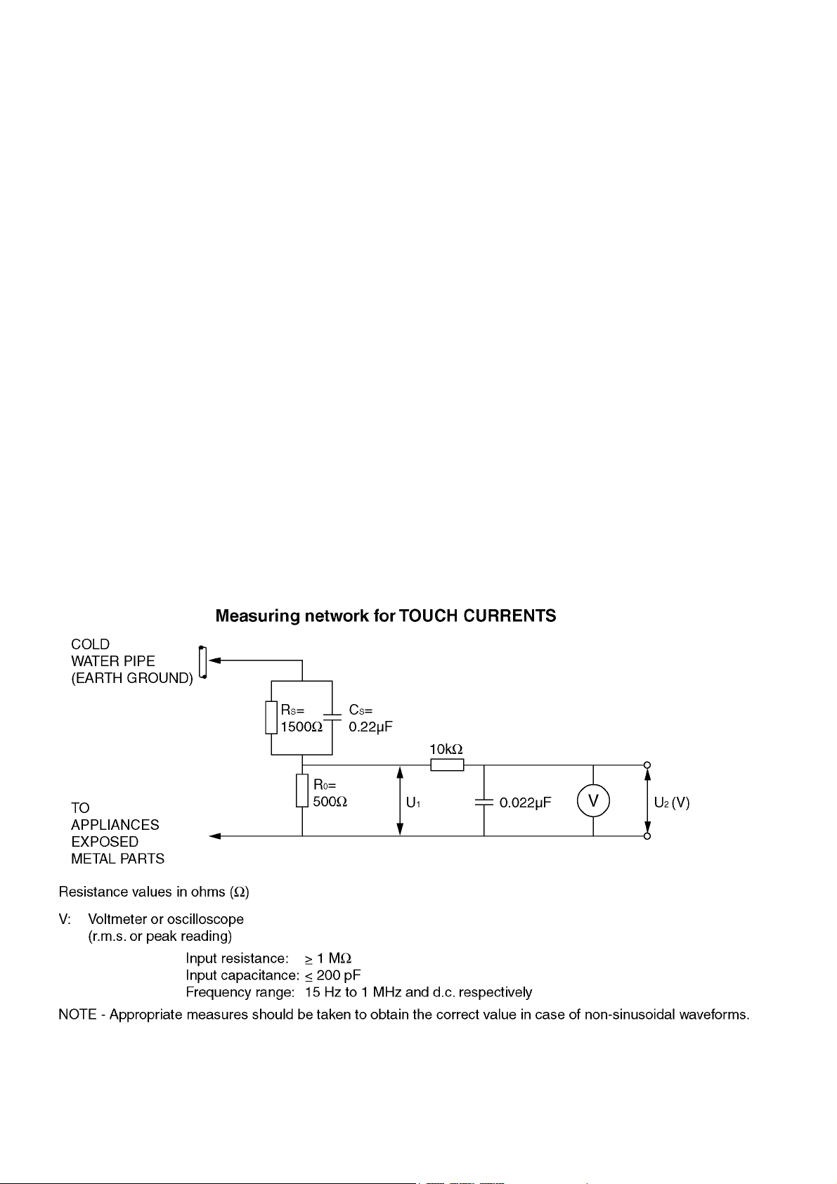
1.2. Touch-Current Check
1. Plug the AC cord directly into the AC outlet. Do not use an isolation transformer for this check.
2. Connect a measuring network for touch currents between each exposed metallic part on the set and a good earth ground
such as a water pipe, as shown in Figure 1.
3. Use Leakage Current Tester (Simpson 228 or equivalent) to measure the potential across the measuring network.
4. Check each exposed metallic part, and measure the voltage at each point.
5. Reserve the AC plug in the AC outlet and repeat each of the above measure.
6. The potential at any point (TOUGH CURRENT) expressed as voltage U
For a. c.: U1 = 35 V (peak) and U2 = 0.35 V (peak);
For d. c.: U1 = 1.0 V,
Note:
The limit value of U
mA d. c.
The limit value U
7. In case a measurement is out of the limits specified, there is a possibility of a shock hazard, and the equipment should be
repaired and rechecked before it is returned to the customer.
= 0.35 V (peak) for a. c. and U1 = 1.0 V for d. c. correspond to the values 0.7 mA (peak) a. c. and 2.0
2
= 35 V (peak) for a. c. correspond to the value 70 mA (peak) a. c. for frequencies greater than 100 kHz.
1
and U2, does not exceed the following values:
1
Figure 1
2
Page 3
2 Warning
2.1. Prevention of Electrostatic Discharge (ESD) to Electrostatically
Sensitive (ES) Devices
Some semiconductor (solid state) devices can be damaged easily by static electricity. Such components commonly are called Electrostatically Sensitive (ES) Devices. Examples of typical ES devices are integrated circuits and some field-effect transistors and
semiconductor [chip] components. The following techniques should be used to help reduce the incidence of component damage
caused by electrostatic discharge (ESD).
1. Immediately before handling any semiconductor component or semiconductor-equipped assembly, drain off any ESD on your
body by touching a known earth ground. Alternatively, obtain and wear a commercially available discharging ESD wrist strap,
which should be removed for potential shock reasons prior to applying power to the unit under test.
2. After removing an electrical assembly equipped with ES devices, place the assembly on a conductive surface such as aluminum foil, to prevent electrostatic charge buildup or exposure of the assembly.
3. Use only a grounded-tip soldering iron to solder or unsolder ES devices.
4. Use only an anti-static solder removal device. Some solder removal devices not classified as [anti-static (ESD protected)] can
generate electrical charge sufficient to damage ES devices.
5. Do not use freon-propelled chemicals. These can generate electrical charges sufficient to damage ES devices.
6. Do not remove a replacement ES device from its protective package until immediately before you are ready to install it. (Most
replacement ES devices are packaged with leads electrically shorted together by conductive foam, aluminum foil or comparable conductive material).
7. Immediately before removing the protective material from the leads of a replacement ES device, touch the protective material
to the chassis or circuit assembly into which the device will be installed.
Caution
Be sure no power is applied to the chassis or circuit, and observe all other safety precautions.
8. Minimize bodily motions when handling unpackaged replacement ES devices. (Otherwise ham less motion such as the brushing together of your clothes fabric or the lifting of your foot from a carpeted floor can generate static electricity (ESD) sufficient
to damage an ES device).
3
Page 4
2.2. About lead free solder (PbF)
Note: Lead is listed as (Pb) in the periodic table of elements.
In the information below, Pb will refer to Lead solder, and PbF will refer to Lead Free Solder.
The Lead Free Solder used in our manufacturing process and discussed below is (Sn+Ag+Cu).
That is Tin (Sn), Silver (Ag) and Copper (Cu) although other types are available.
This model uses Pb Free solder in it’s manufacture due to environmental conservation issues. For service and repair work, we’d
suggest the use of Pb free solder as well, although Pb solder may be used.
PCBs manufactured using lead free solder will have the PbF within a leaf Symbol PbF stamped on the back of PCB.
Caution
• Pb free solder has a higher melting point than standard solder. Typically the melting point is 50 ~ 70 °F (30~40 °C) higher. Please
use a high temperature soldering iron and set it to 700 ± 20 °F (370 ± 10 °C).
• Pb free solder will tend to splash when heated too high (about 1100 °F or 600 °C).
If you must use Pb solder, please completely remove all of the Pb free solder on the pins or solder area before applying Pb solder. If this is not practical, be sure to heat the Pb free solder until it melts, before applying Pb solder.
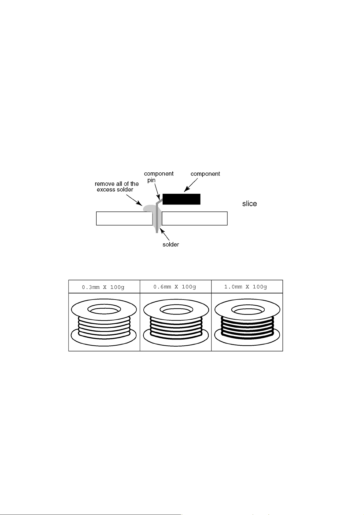
• After applying PbF solder to double layered boards, please check the component side for excess solder which may flow onto the
opposite side. (see figure below)
Suggested Pb free solder
There are several kinds of Pb free solder available for purchase. This product uses Sn+Ag+Cu (tin, silver, copper) solder. However, Sn+Cu (tin, copper), Sn+Zn+Bi (tin, zinc, bismuth) solder can also be used.
4
Page 5
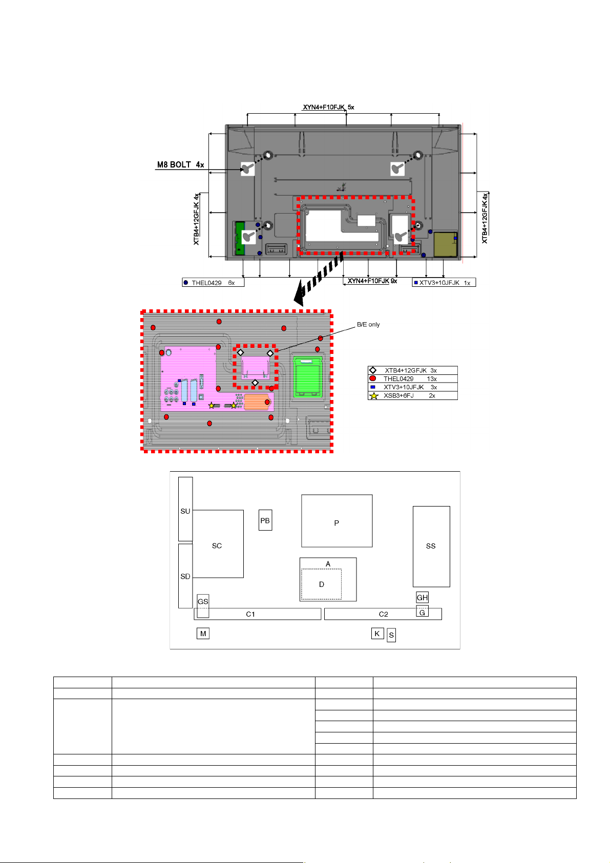
3 Service Navigation
3.1. Service Hint
Board Name Function Board Name Function
P Power Supply C1 Data Driver (Lower Right)
A DC-DC Converter
Speaker out, Sound Processor
AV Terminal, AV Switch
Digital Signal Processor, Micon, HDMI Interface
Peaks Lite 2p
D Format Converter, Plasma AI, Sub-Field Processor GH HDMI3 in
K Remote receiver, Power LED G Side Terminal
S Power Switch M AI Sensor
GS SD Card Slot, Key Switch PB Fan control
C2 Data Driver (Lower Left)
SC Scan Drive
SU Scan out (Upper)
SD Scan out (Lower)
SS Sustain Drive
5
Page 6
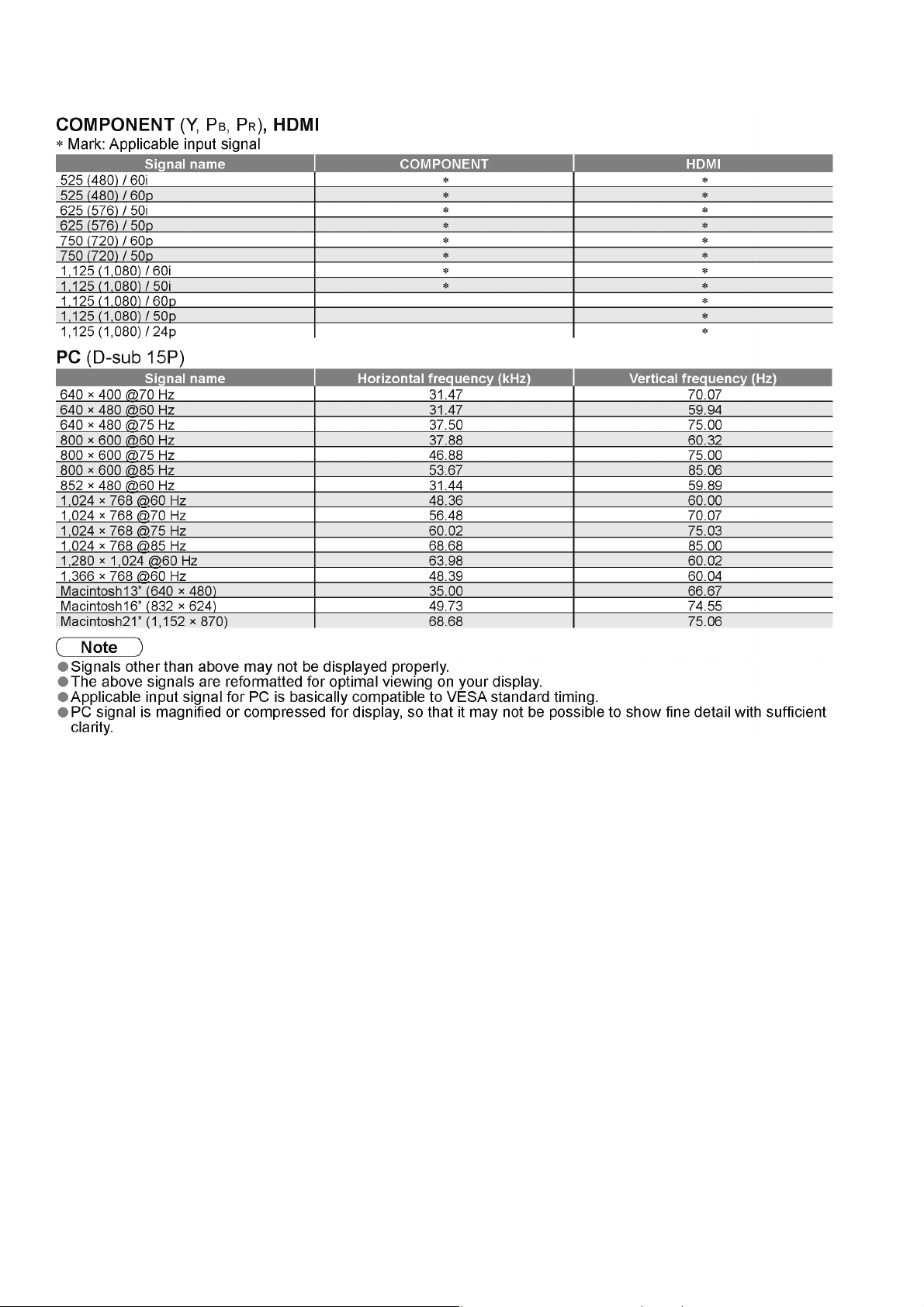
3.2. Applicable signals
6
Page 7

4 Specifications
Power Source AC 220 - 240 V, 50/60 Hz
Power Consumption
Average use 385 W
Standby condition 0.4 W (Without monitor out recording)
Plasma Display panel
Aspect Ratio 16:9
Visible screen size 106 cm (diagonal)
Number of pixels 2,073,600 (1,920 (W) × 1,080 (H)) [5,760 × 1,080 dots]
Sound
Speaker 160 mm × 42 mm × 2 pcs, 8 Ω
Audio Output 20 W (10 W + 10 W), 10% THD
Headphones M3 (3.5 mm) stereo mini Jack × 1
PC signals VGA, SVGA, XGA
Receiving Systems / Band name PAL I : UHF E21-68
(B model) PAL 525/60 : Playback of NTSC tape from some PAL Video recorders (VCR)
(Except B model) PAL B, G, H, I, SECAM B, G, SECAM L/L’ :
Aerial - Rear UHF (B model), VHF/UHF (Except B model)
Operating Conditions
Connection Terminals
AV1 (Scart terminal) 21 Pin terminal (Audio/Video in, Audio/Video out, RGB in, Q-Link)
AV2 (Scart terminal) 21 Pin terminal (Audio/Video in, Audio/Video out, RGB in, S-Video in, Q-Link)
AV3
VIDEO RCA PIN Type × 1 1.0 V [p-p] (75 Ω)
S-VIDEO Mini DIN 4-pin Y:1.0 V [p-p] (75 Ω) C:0.286 V [p-p] (75 Ω)
AUDIO L - R RCA PIN Type × 2 0.5 V [rms]
COMPONENT
VIDEO Y 1.0 V [p-p] (including synchronization)
AUDIO L - R RCA PIN Type × 2 0.5 V [rms]
Others
HDMI1 / 2 / 3 TYPE A Connectors This TV supports “HDAVI Control 3” function.
PC HIGH-DENSITY D-SUB 15PIN R, G, B/ 0.7 V [p-p] (75 Ω)
Card slot SD Card slot × 1
Output
AUDIO L - R RCA PIN Type × 2 0.5 V [rms] (high impedance)
DIGITAL AUDIO OUT PCM/Dolby Digital, Fiber optic
Dimensions (W × H × D) 1,064 mm × 723 mm × 327 mm (With Pedestal)
Mass 34.0 kg Net (With Pedestal)
20 W (With monitor out recording)
922 mm (W) × 518 mm (H)
SXGA ....... (compressed)
Horizontal scanning frequency 31 - 69 kHz
Vertical scanning frequency 59 - 86 Hz
or NTSC disc playback from DVD player and recorder.
DVB : Digital terrestrial services via UHF aerial input.
M.NTSC : Playback from M.NTSC Video recorders (VCR).
NTSC (AV input only) : Playback from NTSC Video recorders (VCR).
VHF E2 - E12 VHF H1 - H2 (ITALY)
VHF A - H (ITALY) UHF E21 - E69
CATV (S01 - S05) CATV S1 - S10 (M1 - M10)
CATV S11 - S20 (U1 - U10) CATV S21 - S41 (Hyperband)
PAL D, K, SECAM D, K :
VHF R1 - R2 VHF R3 - R5
VHF R6 - R12 UHF E21 -E69
PAL 520/60 : Playback of NTSC tape from some PAL Video recorders (VCR)
DVB : Digital terrestrial services via VHF / UHF aerial input.
M.NTSC : Playback from M. NTSC Video recorders (VCR)
NTSC (AV input only) : Playback from NTSC Video recorders (VCR)
TV signals may not be received in some areas.
Temperature: 0 °C - 35 °C
Humidity: 20 % - 80 % RH (non-condensing)
, P
P
B
R
1,064 mm × 674 mm × 92 mm (TV only)
30.0 kg Net (TV only)
± 0.35 V [p-p]
HD, VD/TTL Level 2.0 - 5.0 V [p-p] (high impedance)
7
Page 8

Note
• Design and Specifications are subject to change without notice. Mass and Dimensions shown are approximate.
• This equipment complies with the EMC standards listed below.
EN55013, EN61000-3-2, EN61000-3-3, EN55020, EN55022, EN55024.
8
Page 9

5 Service Mode
5.1. How to enter into Service Mode
While pressing [VOLUME ( - )] button of the main unit, press [0] button of the remote control three times within 2 seconds.
5.1.1. Key command
[1] button...Main items Selection in forward direction
[2] button...Main items Selection in reverse direction
[3] button...Sub items Selection in forward direction
[4] button...Sub items Selection in reverse direction
[RED] button...All Sub items Selection in forward direction
[GREEN] button...All Sub items Selection in reverse direction
[VOL] button...Value of sub items change in forward direction ( + ), in reverse direction ( - )
9
Page 10
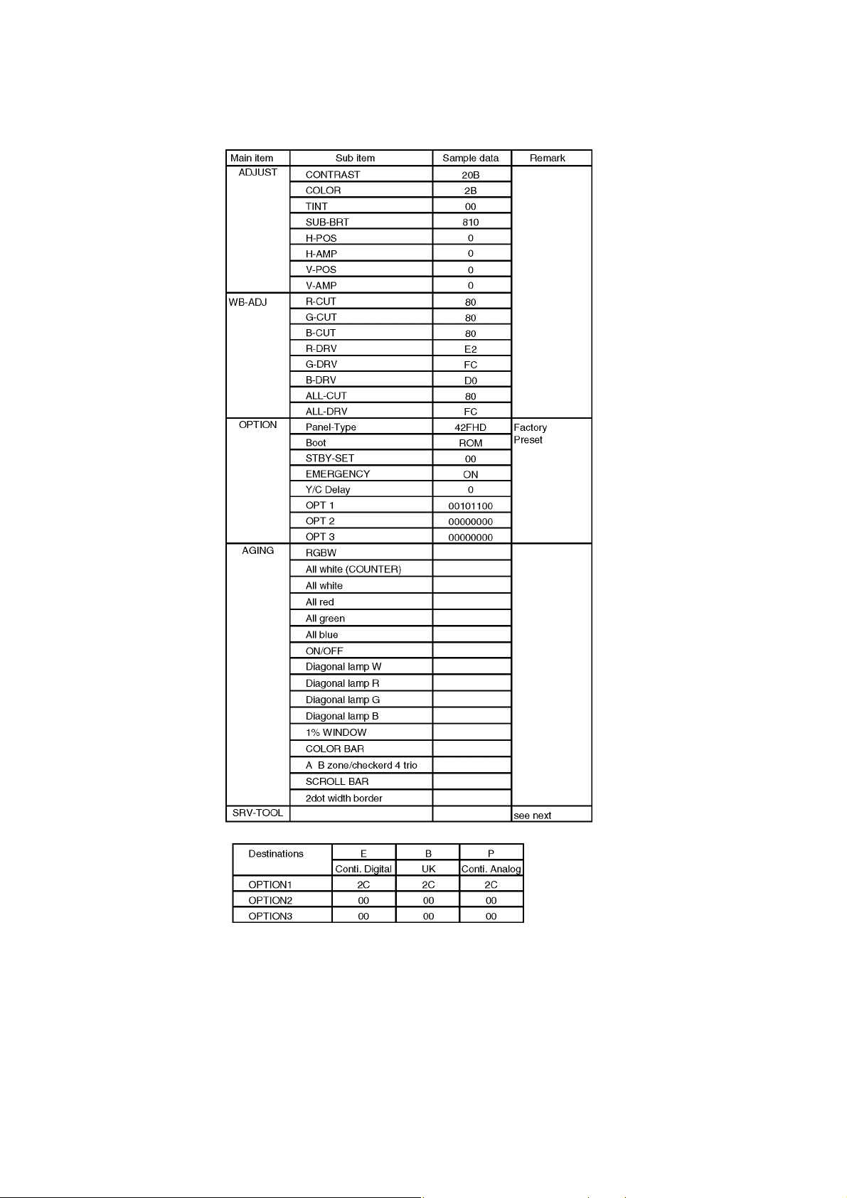
5.1.2. Contents of adjustment mode
• Value is shown as a hexadecimal number.
• Preset value differs depending on models.
• After entering the adjustment mode, take note of the value in each item before starting adjustment.
5.1.3. How to exit
Switch off the power with the [POWER] button on the main unit or the [POWER] button on the remote control.
10
Page 11
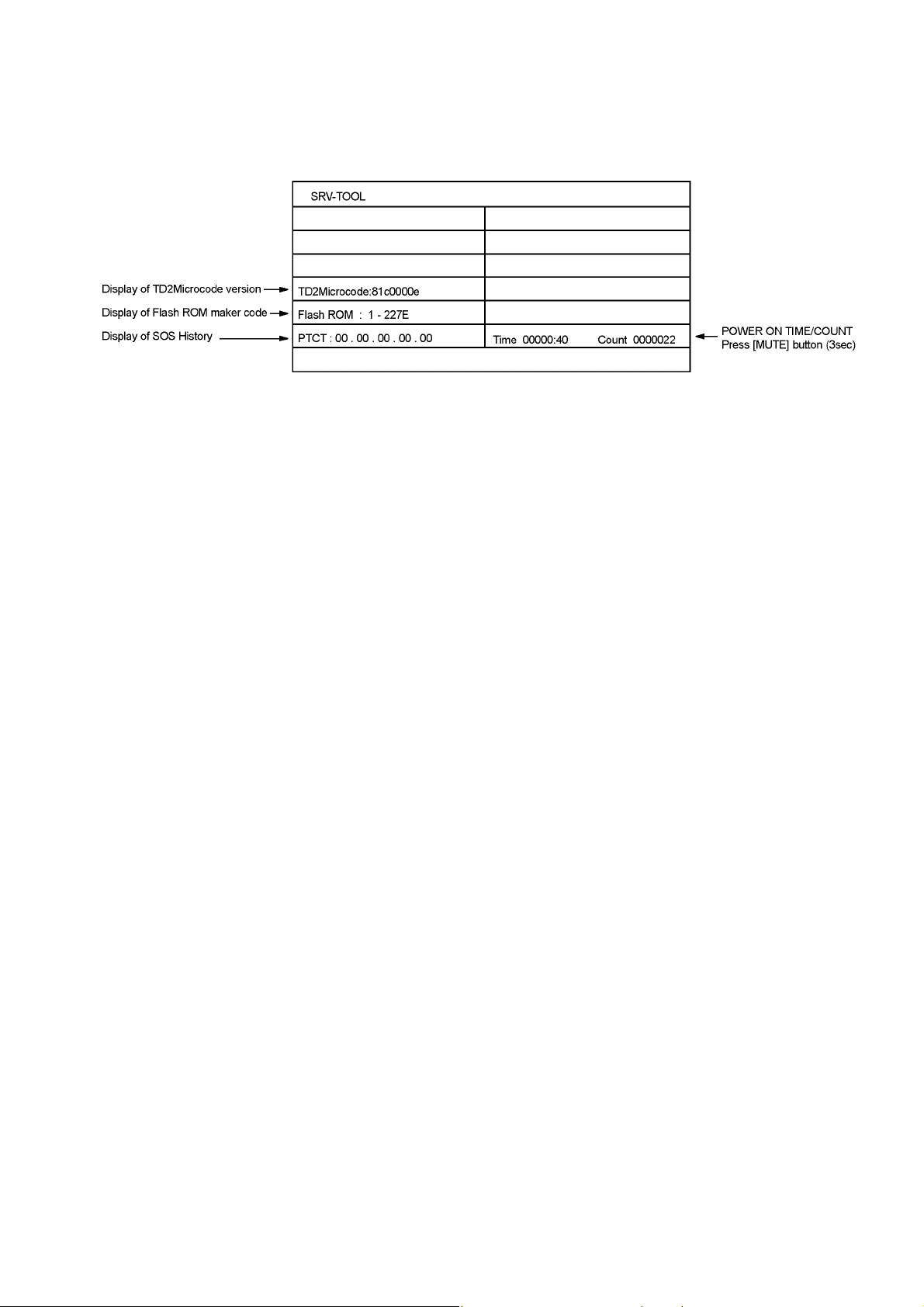
5.2. Service tool mode
5.2.1. How to access
1. Select [SRV-TOOL] in Service Mode.
2. Press [OK] button on the remote control.
5.2.2. Display of SOS History
SOS History (Number of LED blinking) indication.
From left side; Last SOS, before Last, three occurrence before, 2nd occurrence after shipment, 1st occurrence after shipment.
This indication except 2nd and 1st occurrence after shipment will be cleared by [Self-check indication and forced to factory shipment setting].
5.2.3. POWER ON TIME/COUNT
To display TIME/COUNT menu, highlight position, then press MUTE for 3sec.
Time : Cumulative power on time, indicated hour : minute by decimal
Count : Number of ON times by decimal
Note : This indication will not be cleared by either of the self-check or any command.
5.2.4. Exit
1. Disconnect the AC cord from wall outlet or switch off the power with the [POWER] button on the main unit.
11
Page 12
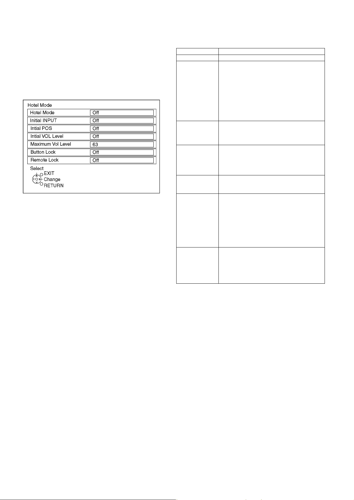
5.3. Hotel mode
1. Purpose
Restrict a function for hotels.
Access command to the Hotel mode setup menu
In order to display the Hotel mode setup menu, please
enter the following command (within 2 second).
[TV] : Vol. [Down] + [REMOTE] : AV (3 times)
Then, the Hotel mode setup menu is displayed.
2. To exit the Hotel mode setup menu
Disconnect AC power cord from wall outlet or switch off
the power with the [POWER] button on the main unit.
3. Explain the Hotel mode setup menu
item Function
Hotel Mode Select hotel mode ON/OFF
Initial INPUT Select input signal modes.
Set the input, when each time power is switched
on.
Selection :
Off/Analogue/DVB/AV1/AV2/AV2S/AV3/AV3S/
Comp./PC/HDMI1/HDMI2/HDMI3
• Off: give priority to a last memory. However,
Euro model is compulsorily set to TV.
• AVnS/AVnC: only Euro model selectable
• PC: selectable with VGA option
Initial POS Select programme number.
Selection :
Off/0 to 99
• Off: give priority to a last memory
Initial VOL level Adjust the volume when each time power is
switched on.
Selection/Range :
Off/0 to 63
• Off: give priority to a last memory
Maximum VOL
level
Button lock Select local key conditions.
Remote lock Select remote control key conditions.
Adjust maximum volume.
Range :
0 to 63
Selection :
Off/SETUP/MENU/All
• Off: altogether valid
• SETUP: only F-key is invalid
(Tuning guide(menu) can not be selected.)
• MENU: only F-key is invalid
(only Volume/Mute can be selected.)
• ALL: altogether invalid.
Selection :
Off/SETUP/MENU
• Off: altogether valid
• SETUP: only Setup menu is invalid
• MENU: Picture/Sound/Setup menu are invalid
12
Page 13
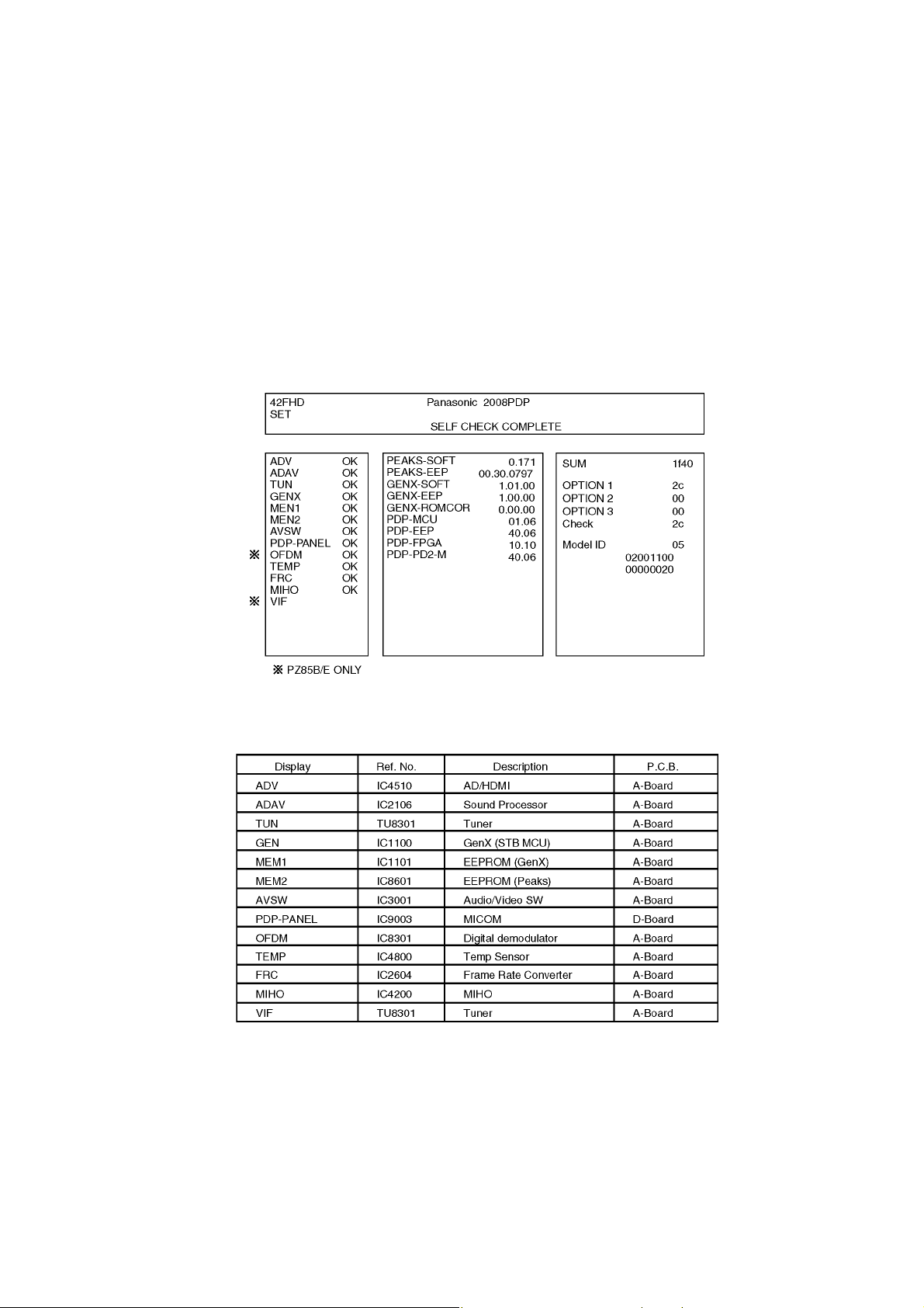
6 Troubleshooting Guide
Use the self-check function to test the unit.
1. Checking the IIC bus lines
2. Power LED Blinking timing
6.1. Check of the IIC bus lines
6.1.1. How to access
Self-check indication only:
Produce TV reception screen, and while pressing [VOLUME ( - )] button on the main unit, press [OK] button on the remote control
for more than 3 seconds.
Self-check indication and forced to factory shipment setting:
Produce TV reception screen, and while pressing [VOLUME ( - )] button on the main unit, press [MENU] button on the remote con-
trol for more than 3 seconds.
6.1.2. Screen display
6.1.3. Check Point
Confirm the following parts if NG was displayed.
6.1.4. Exit
Disconnect the AC cord from wall outlet or switch off the power with the [POWER] button on the main unit.
13
Page 14
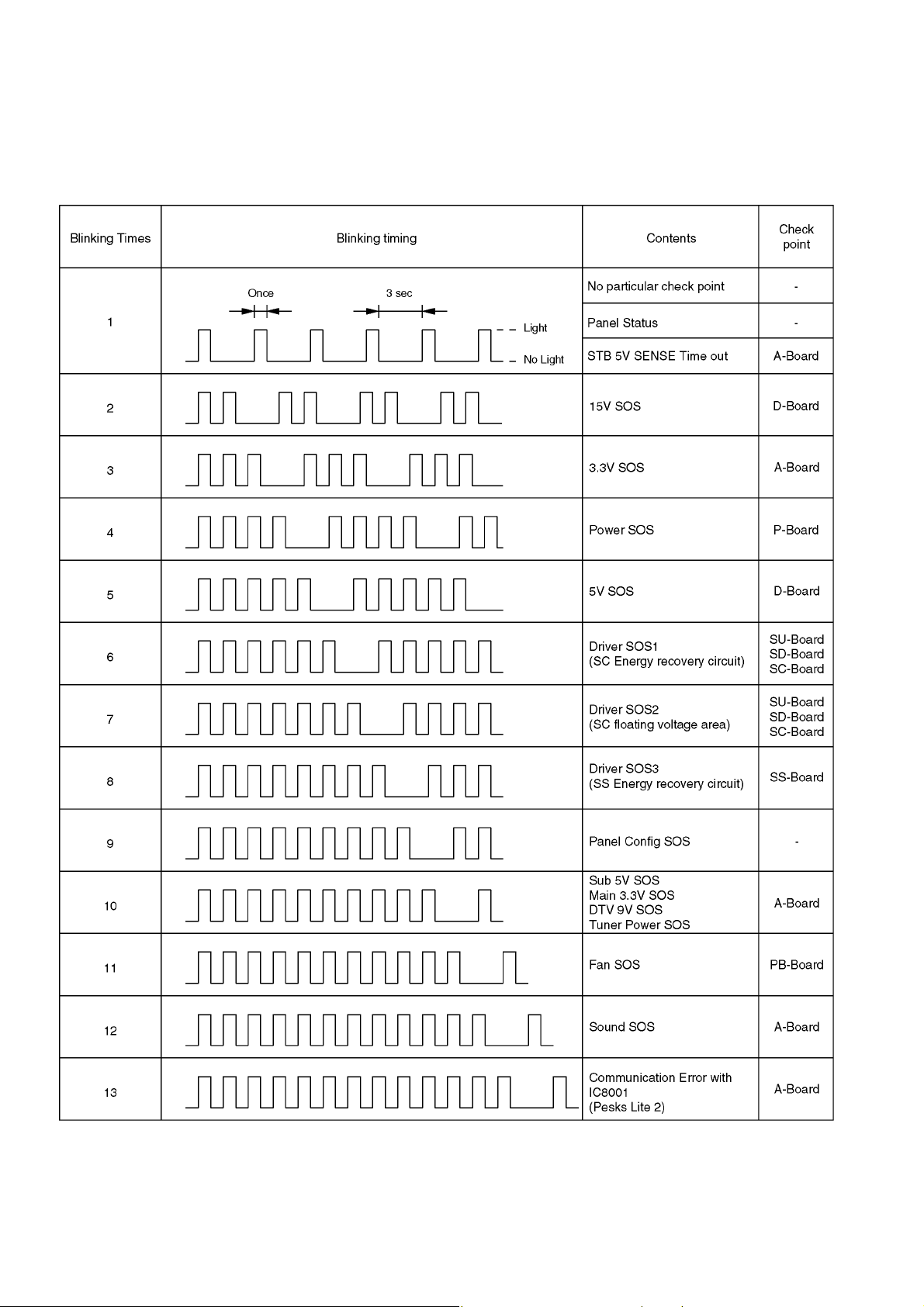
6.2. Power LED Blinking timing chart
1. Subject
Information of LED Flashing timing chart.
2. Contents
When an abnormality has occurred the unit, the protection circuit operates and reset to the stand by mode. At this time, the
defective block can be identified by the number of blinks of the Power LED on the front panel of the unit.
14
Page 15
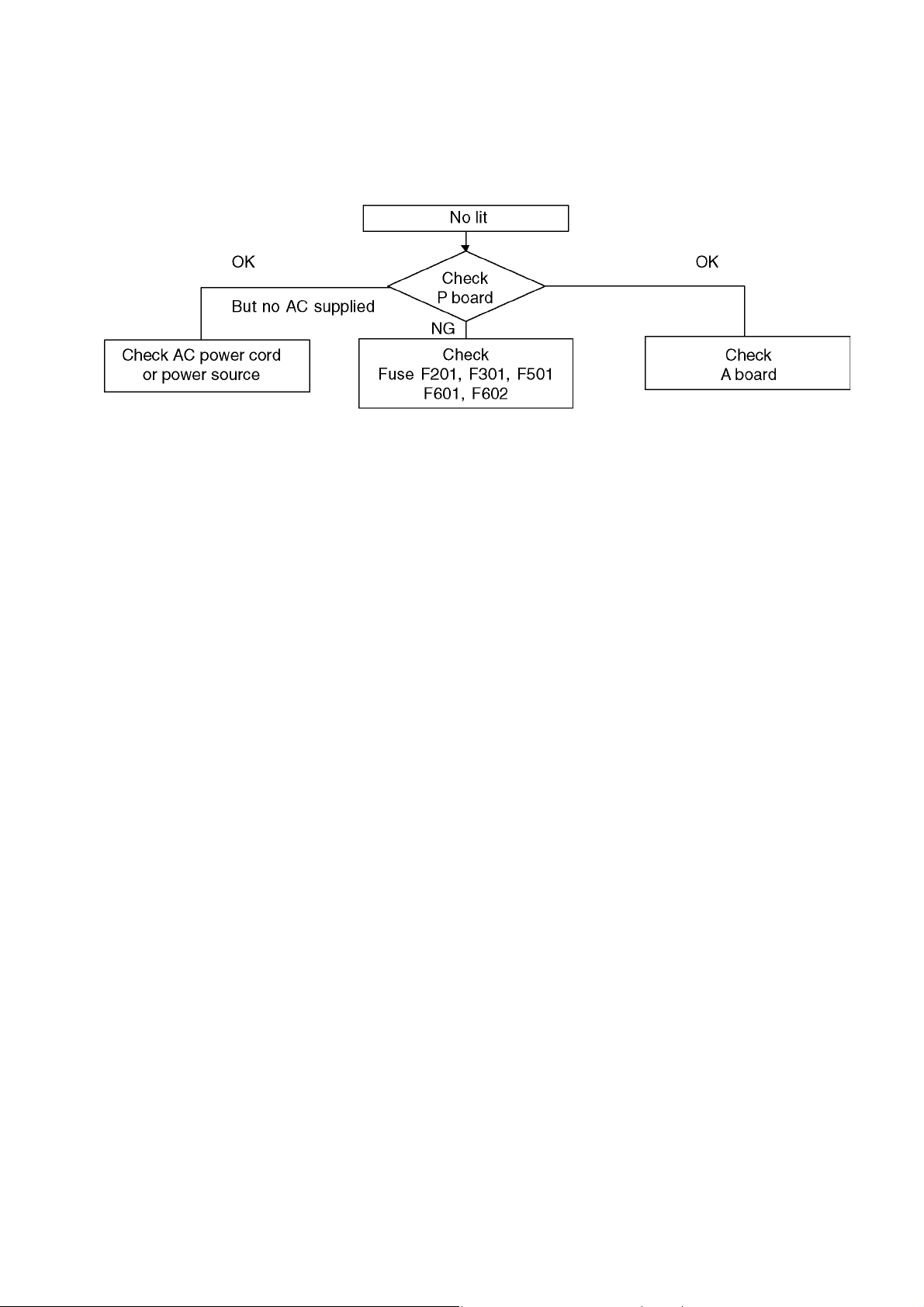
6.3. No Power
First check point
There are following 2 states of No Power indication by power LED.
1. No lit
2. Red is lit then turns red blinking a few seconds later. (See 6.2.)
15
Page 16
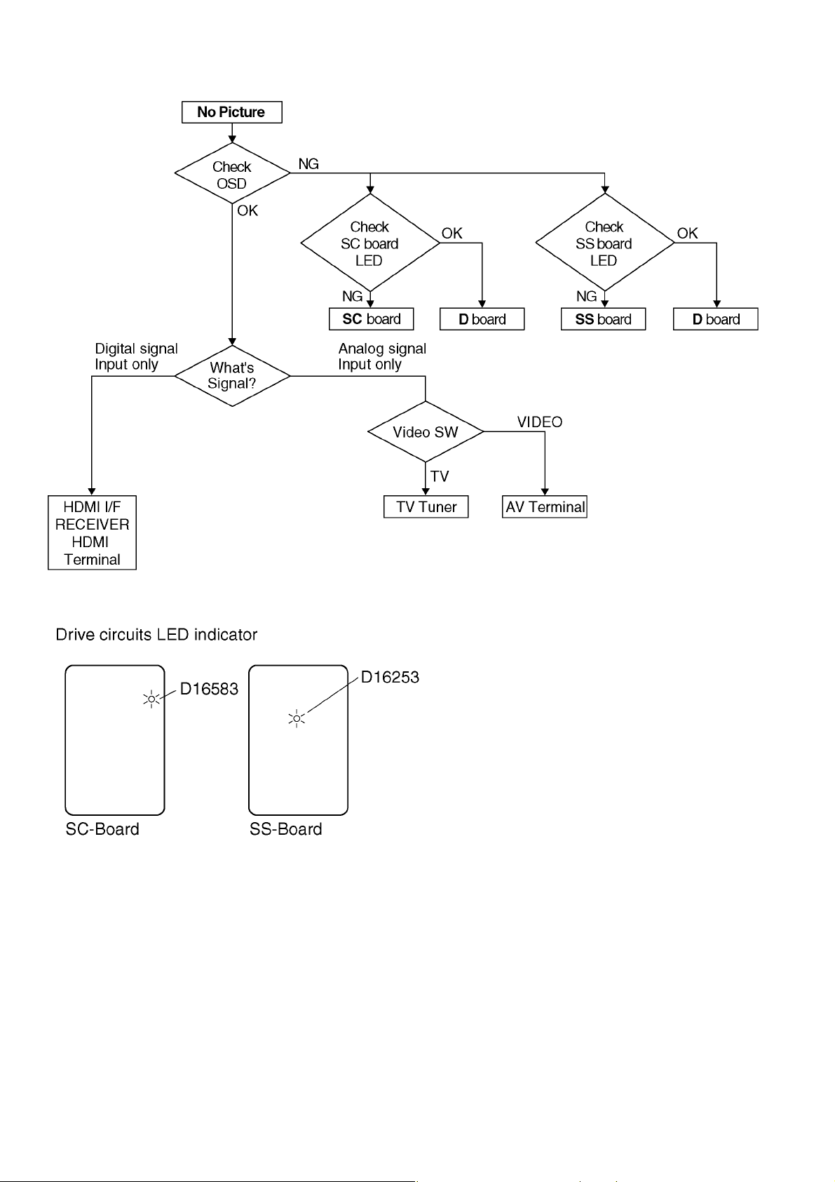
6.4. No Picture
16
Page 17
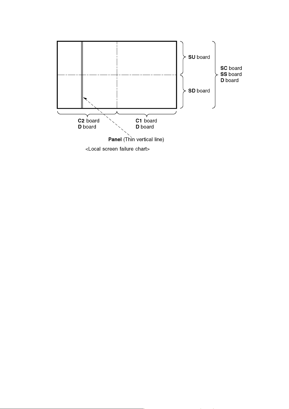
6.5. Local screen failure
Plasma display may have local area failure on the screen. Fig-1 is the possible defect P.C.B. for each local area.
Fig-1
17
Page 18
7 Disassembly and Assembly Instructions
7.1. Remove the Rear cover
1. See Service Hint (Section 3)
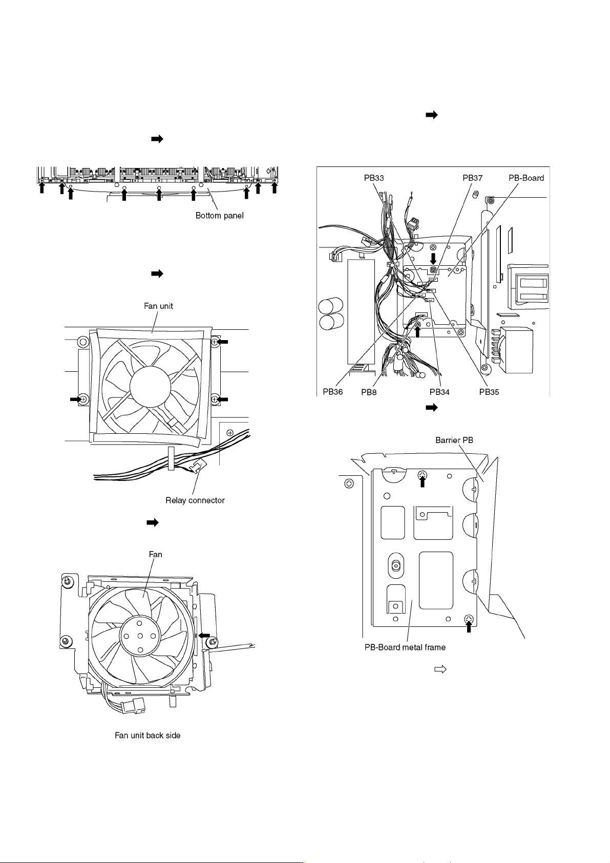
7.2. Remove the Bottom panel
1. Remove the screws (×9 ).
2. Remove the Bottom panel.
7.3. Remove the Fan unit
1. Unlock the cable clampers to free the cable.
2. Remove the screws (×3 ).
3. Remove the relay connectors and remove the Fan unit.
7.4. Remove the PB-Board
1. Unlock the cable clampers to free the cable.
2. Remove the screws (×2 ).
3. Disconnect the connectors (PB8, PB33, PB35, PB36 and
PB37)
4. Remove the PB-Board.
4. Remove the screw (×1 ) on the back side.
5. Remove the Fan.
5. Remove the screws (×2 ).
6. Remove the PB-Board metal frame.
7. Remove the clampers (×3 ).
18
Page 19
8. Remove the barrier (PB).
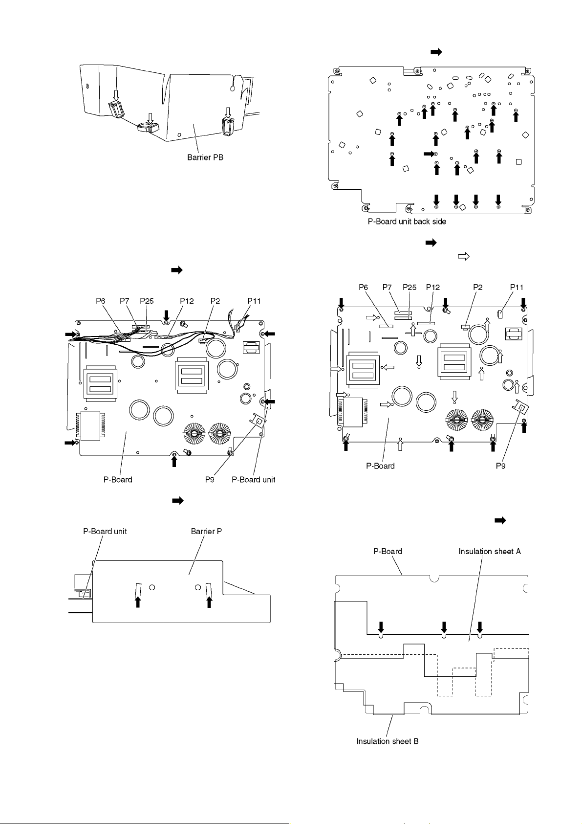
7.5. Remove the P-Board
Caution:
To remove P.C.B. wait 1 minute after power was off for discharge from electrolysis capacitors.
1. Unlock the cable clampers to free the cable.
2. Disconnect the couplers (P2, P6, P7, P9, P11, P12 and
P25).
3. Remove the screws (×6 ) and remove the P-Board
unit.
6. Remove the screws (×20 ) on the back side.
7. Remove the screws (×7 ).
8. Remove the molding props (×13 ).
9. Remove the P-Board.
4. Remove the clampers (×2 ).
5. Remove the barrier (P).
Note:
When assembling the P-Board, the position of each hole of
the insulation sheets (A and B) is set to the position of each
hole of the P-Board, then assemble them. ( marks indicate setting positions.)
19
Page 20
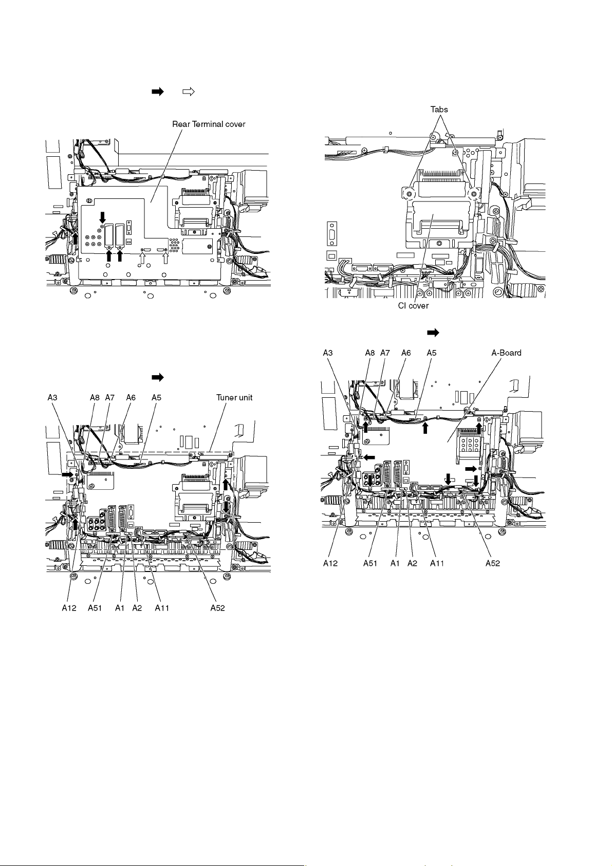
7.6. Remove the Rear Terminal
cover
1. Remove the screws (×3 , ×2 ).
2. Remove the Rear Terminal cover.
7.8. Remove the A-Board
1. Remove the Tuner unit. (See section 7.7.)
2. Remove the 2 tabs and remove the CI cover.
7.7. Remove the Tuner unit
1. Unlock the cable clampers to free the cable.
2. Disconnect the connectors (A1, A2, A3 , A5, A6, A7, A8,
A11, A12, A51 and A52).
3. Remove the screws (×4 ) and remove the Tuner unit.
3. Remove the screws (×8 ) and remove the A-Board.
20
Page 21
7.9. Remove the Side control unit
assy
1. Disconnect the connectors (A52). (See section 7.7.)
2. Remove the screws (×4 ) and remove the Side control
unit assy.
metal frame.
6. Remove the screws (×2 ) and remove the Side control
panel bottom and the Control button.
7.10. Remove the GS-Board and the
Control button
1. Remove the Side control unit assy. (See section 7.9.)
2. Remove the screws (×2 ).
3. Disconnect the connectors (GS52) and remove the GSBoard.
4. Remove the screws (×2 )
5. Remove the Side control mount metal from Side control
21
Page 22
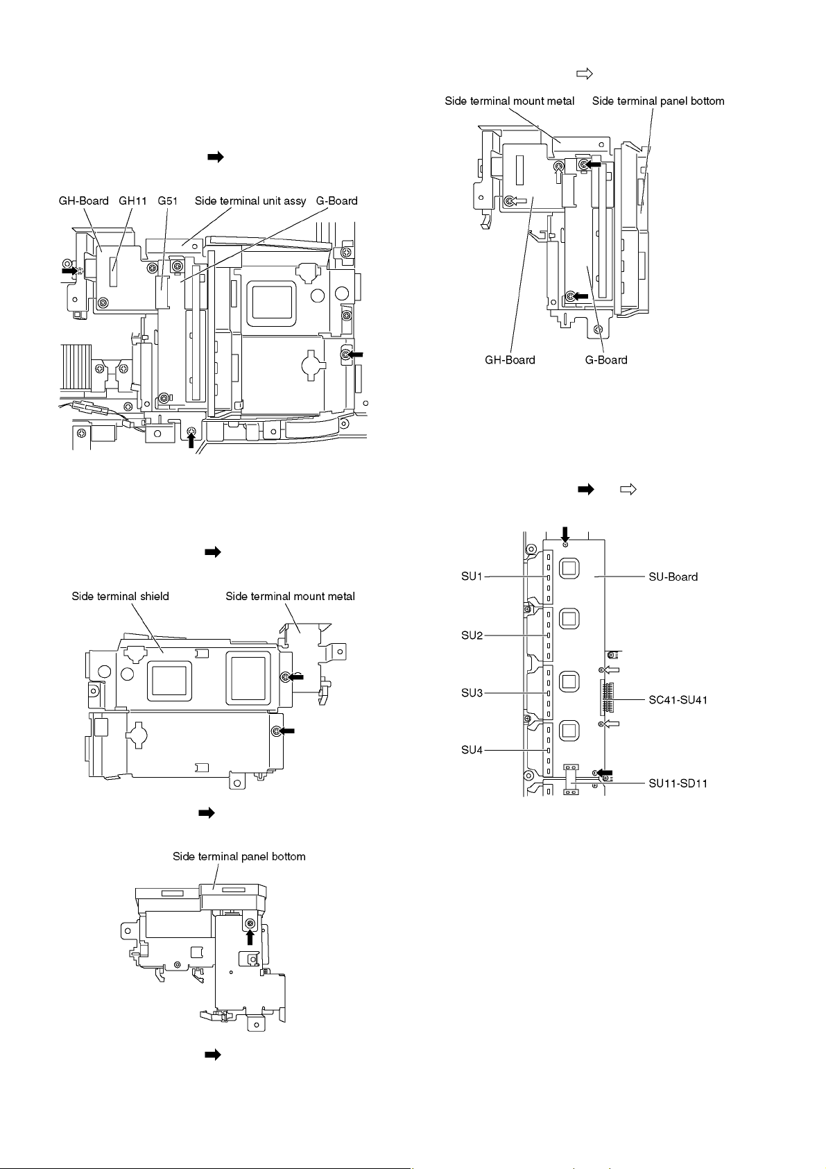
7.11. Remove the Side terminal unit
assy
1. Unlock the cable clampers to free the cable.
2. Disconnect the connectors (GH11 and G51).
3. Remove the screws (×3 ) and remove the Side terminal unit assy.
7.12. Remove the G-Board and the
GH-board
1. Remove the Side terminal unit assy. (See section 7.11.)
2. Remove the screws (×2 ) from back side.
3. Remove the Side terminal shield.
6. Remove the screws (×2 ) and remove the GH-Board.
7.13. Remove the SU-Board
1. Remove the flexible cables (SU1, SU2, SU3 and SU4)
connected to the SU-Board.
2. Remove the flexible cable (SU11-SD11) and the bridge
connector (SC41-SU41).
3. Remove the screws (×2 , ×2 ) and remove the SU-
Board.
4. Remove the screw (×1 ) and remove the Side terminal
panel bottom.
5. Remove the screws (×2 ) and remove the G-Board.
22
Page 23
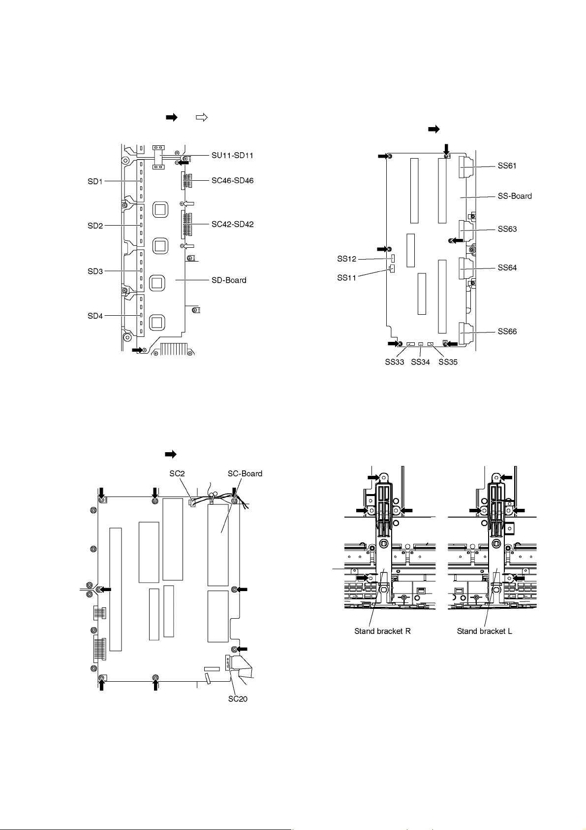
7.14. Remove the SD-Board
1. Remove the flexible cables (SD1, SD2, SD3 and SD4)
connected to the SD-Board.
2. Remove the flexible cable (SU11-SD11) and the bridge
connectors (SC42-SD42 and SC46-SD46).
3. Remove the screws (×2 , ×2 ) and remove the SD-
Board.
7.16. Remove the SS-Board
1. Unlock the cable clampers to free the cable.
2. Disconnect the connectors (SS11, SS12, SS33, SS34
and SS35).
3. Disconnect the flexible cables (SS61, SS63, SS64 and
SS66).
4. Remove the screws (×6 ) and remove the SS-Board.
7.15. Remove the SC-Board
1. Remove the SU-Board and SD-Board. (See section 7.13.
and 7.14.)
2. Unlock the cable clampers to free the cable.
3. Disconnect the connector (SC2).
4. Disconnect the flexible cable (SC20).
5. Remove the screws (×8 ) and remove the SC-Board.
7.17. Remove the Stand brackets
1. Remove the Plasma panel section from the servicing
stand and lay on a fiat surface such as a table (covered)
with the Plasma panel surface facing downward.
2. Remove the Stand brackets (L, R) fastening screws (×4
each) and remove the Stand brackets (L, R).
23
Page 24
7.18. Remove the D-Board
1. Remove the Tuner unit. (See section 7.7.)
2. Disconnect the connectors (D3, D5 and D25).
3. Disconnect the flexible cables (D20, D31, D32 and D33).
4. Remove the screws (×4 ) and remove the D-Board.
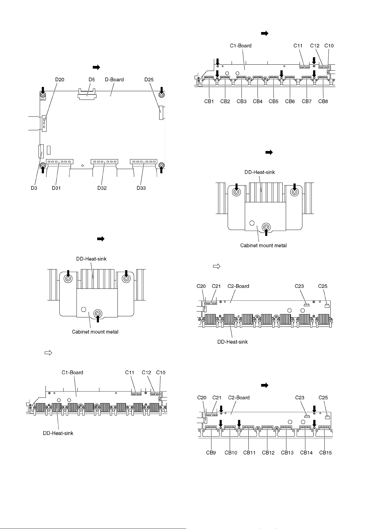
7.19. Remove the C1-Board
1. Remove the Tuner unit. (See section 7.7.)
2. Remove the Side control unit assy. (See section 7.9.)
3. Remove the Stand bracket R. (See section 7.17.)
4. Remove the screws (×3 ) and Remove the Cabinet
mount metal.
9. Remove the screws (×5 ) and remove the C1-Board.
7.20. Remove the C2-Board
1. Remove the Tuner unit. (See section 7.7.)
2. Remove the Side terminal unit assy. (See section 7.11.)
3. Remove the stand bracket L. (See section 7.17.)
4. Remove the screws (×3 ) and Remove the Cabinet
mount metal.
5. Remove the DD-Heat-sink holder fastening screws
(×16 ).
6. Remove the DD-Heat-sink (×8).
5. Remove the DD-Heat-sink holder fastening screws
(×14 ).
6. Remove the DD-Heat-sink (×7).
7. Disconnect the flexible cables (CB9, CB10, CB11, CB12,
CB13, CB14 and CB15).
8. Disconnect the flexible cables (C20 and C21).
9. Disconnect the connectors (C23 and C25).
10. Remove the screws (×5 ) and remove the C2-Board.
7. Disconnect the flexible cables (CB1, CB2, CB3, CB4,
CB5, CB6, CB7 and CB8).
8. Disconnect the flexible cables (C10, C11 and C12).
24
Page 25
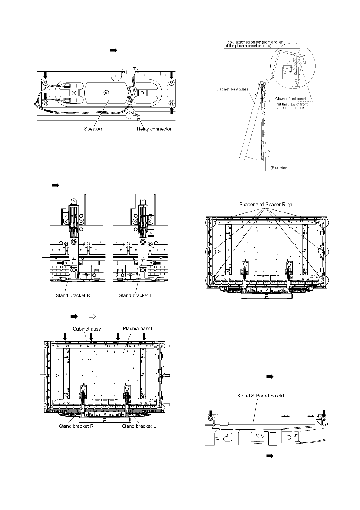
7.21. Remove the Speakers
1. Disconnect the relay connectors
2. Remove the screws (×4 each) and remove the
Speaker (L, R).
7.22. Remove the Plasma panel section from the Cabinet assy
(glass)
1. Remove the stand brackets (left, right) fastening screw
(×1 each).
bottom of the cabinet assy forward, lift, and remove.
4. Remove the 6 Spacers and Spacer Rings from the
Plasma Panel.
2. Remove the cabinet assy and the plasma panel fastening
screws (×4 , ×6 ).
3. For leaving the plasma panel from the front frame, pull the
Caution:
• Please confirm the installation place of Spacer and
Spacer Ring when you exchange the Plasma Panel, and
install Spacer and Spacer Ring in an original installation
place after exchanging the Plasma Panel.
7.23. Remove the K-Board and SBoard
1. Remove the Cabinet assy. (See section 7.22.)
2. Remove the screws (×2 ) and remove the K and SBoard shield.
3. Remove the screws (×3 ) and remove the K and S-
25
Page 26
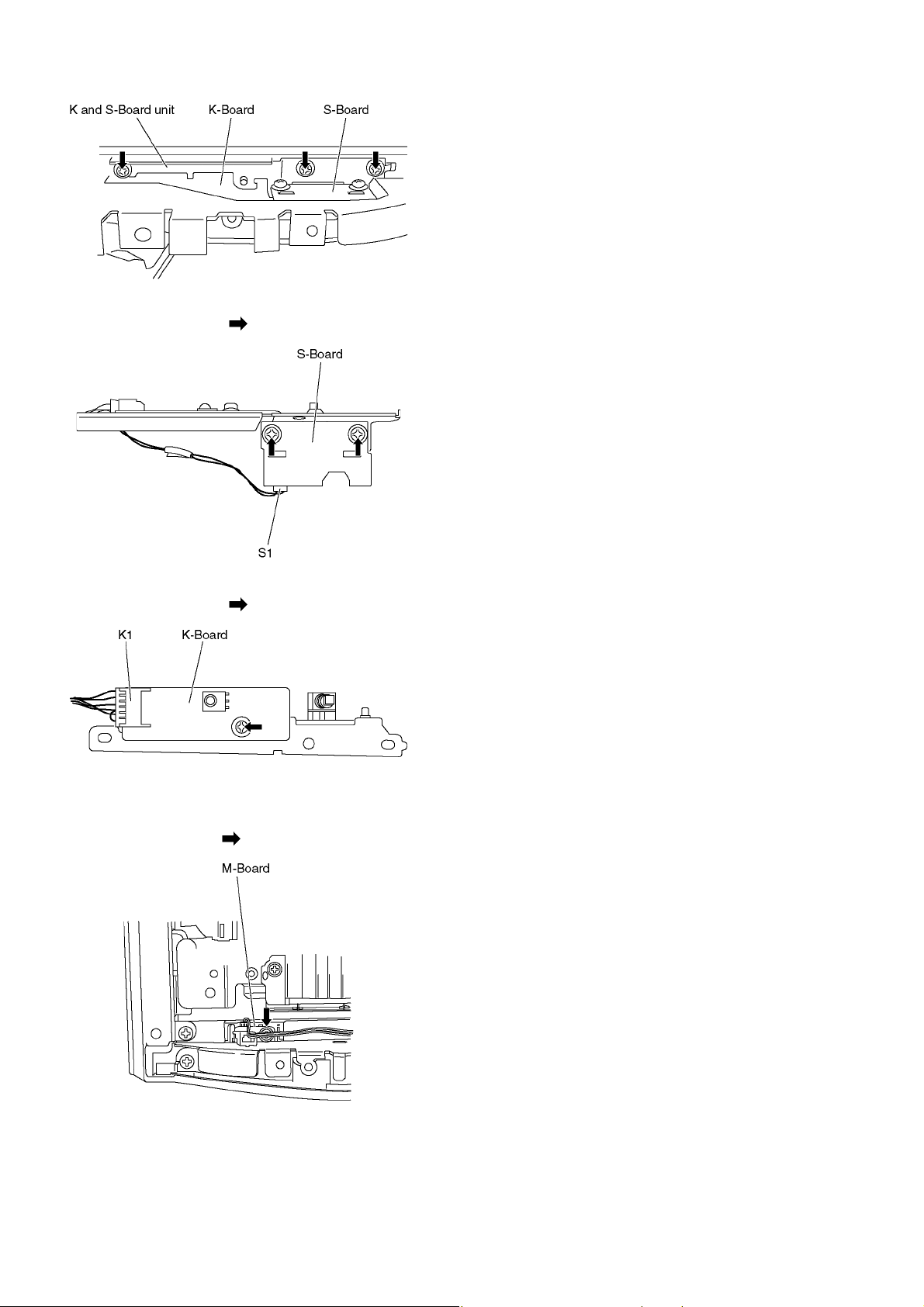
Board unit.
4. Disconnect the connector (S1).
5. Remove the screws (×2 ) and remove the S-Board.
7.25. Remove the plasma panel (finished)
1. Place the new plasma panel (finished) on the flat surface
of the table (covered by a soft cloth), with the plasma
panel surface facing downward.
2. Attach the C1-Board and the C2-Board, connect the flexible cables (×15) from the plasma panel to the C1-Board
and the C2-Board, and fit the flexible cable holders.
3. Attach the Hooks (left, right) and fit the stand brackets (L,
R) to the new plasma panel.
4. Place the plasma panel section on the servicing stand.
5. Attach the cabinet assy and each P.C.Board and so on, to
the new plasma panel.
*When fitting the cabinet assy, be careful not to allow
any debris, dust or handling residue to remain
between the front glass and plasma panel.
6. Disconnect the connector (K1).
7. Remove the screws (×1 ) and remove the K-Board.
7.24. Remove the M-Board
1. Remove the Side terminal unit assy. (See section 7.11.)
2. Remove the screw (×1 ) and remove the M-Board.
26
Page 27
8 Measurements and Adjustments
8.1. Adjustment Procedure
8.1.1. Driver Set-up
8.1.1.1. Item / Preparation
1. Input a white signal to plasma video input.
2. Set the picture controls as follows.
Picture menu: Dynamic
PNR: OFF
Aspect: 16:9
Caution
1. First perform Vsus adjustment.
2. Confirmation of Vscn voltage should be performed after
confirmation of Vad adjustment.
When Vad= -140V, Voltage of Vscn is 8V ±1V.
8.1.1.2. Adjustments
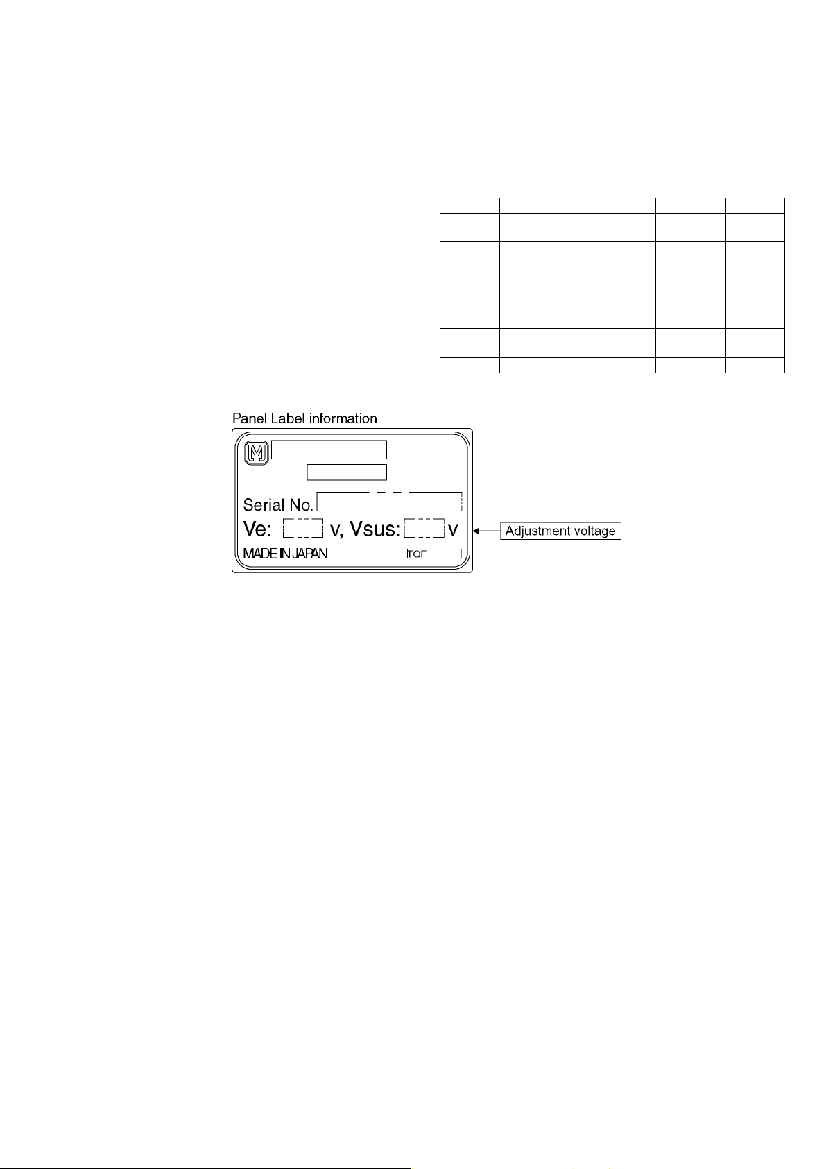
Adjust driver section voltages referring the panel data on the
panel data label.
Check or adjust the following voltages with the multimeter.
Name Test Point Voltage Volume Remarks
Vsus TPVSUS
(SS)
Ve TPVE (SS) Ve ± 1V VR16000
Vset TPVSET
(SC)
Vad TPVAD (SC) -140V ± 1V VR16600
Vscn TPVSCN
(SC)
Vda TPVDA (SS) 75V + 1V, -2V Fixed
*See the Panel label.
Vsus ± 2V VR251 (P) *
*
(SS)
330V ± 7V Fixed
(SC)
Vad+148V ± 1V Fixed
27
Page 28

8.1.2. Initialization Pulse Adjust
1. Input the White signal to plasma video input.
2. Set the picture controls as follows.
Picture menu : Dynamic
PNR : OFF
Aspect : 16:9
3. Connect Oscilloscope to TPSC1 (SC).
Check the voltage (T2) at 100 us period on the down slop.
Test point Volume Level
T2 TPSC1 (SC) VR16602 (SC) 250 V ± 10 V
8.1.3. P.C.B. (Printed Circuit Board) exchange
8.1.3.1. Caution
1. To remove P.C.B. , wait 1 minute after power was off for discharge from electrolysis capacitors.
8.1.3.2. Quick adjustment after P.C.B. exchange
Adjust the following voltages with the multimeter.
P.C.B. Name Test Point Voltage Volume Remarks
P Board Vsus TPVSUS (SS) Vsus ± 2V VR251 (P) *
SC Board Vad TPVAD (SC) -140V ± 1V VR16600 (SC)
SS Board Ve TPVE (SS) Ve ± 1V VR16000 (SS) *
*See the Panel label.
Caution:
Absolutely do not reduce Vsus below Ve not to damage the P.C.B.
28
Page 29
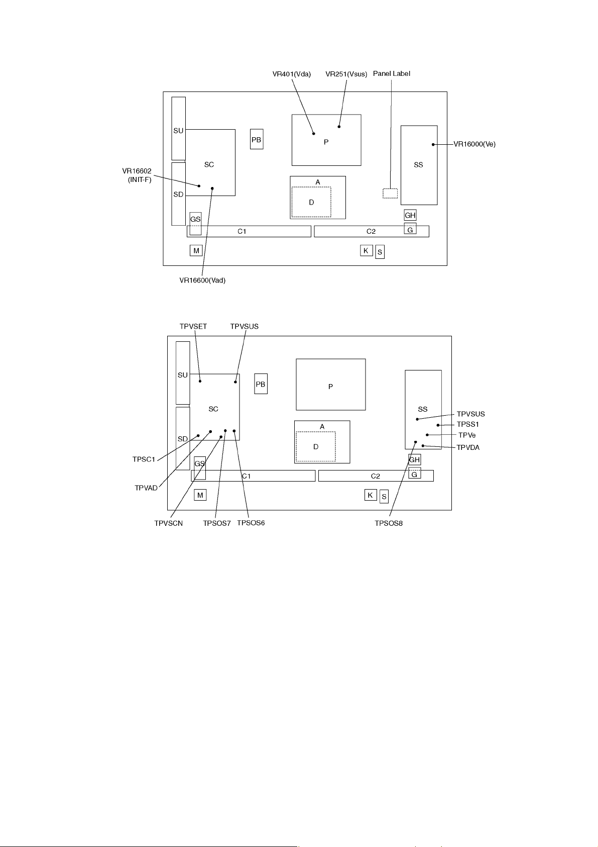
8.1.4. Adjustment Volume Location
8.1.5. Test Point Location
29
Page 30

30
Page 31

9 Block Diagram
A3
+30V(BT)
REMOTE
RECEIVER
FAN SOS DET
+3.3V(S)
G
AUDIO
AI SENSOR
to D5
L,R
FAN CONT
+3.3V(S)
SUB+1.2V
K1
GS52
Y,C , V
B/E ONLY
SD BOOT
+3.3V(STB)
CH0 DATA
KEYSCAN1
M
GH11
A8
RESET
SPEAKER(L)
A52
+3.3V(FHD)
VIDEO SW
FRC+1V
AV3
CIRCUIT
FRC-H
CI SLOT
AUDIO AMP
DCDC
AI SENSOR
A11
FAN SOS
+3.3V(S)
SOUND SOS
REMOTE RECEIVER
OUT
+2.6V(FRC)
from
HDMI I/F
RECEIVER
PROCESSOR
+15V(SND)
OPTICAL OUT
ALL OFF
+3.3V(STB)
+15V(FAN)
HDMI3 IN
PWM AUDIO OUT
TUNER
RESETY,C , V
FAN_A-D
+5V(S)
SD CARD SLOT
SOUND
EEPROM
TUNER SOS
GS
PC
+2.5V(FRC)
A6
PB
F+15V
PB34
FHD+3.3V
+9V(P)
PB8
FLASH
Local 16bit OSD
AI SENSOR
+5V(S)
L,R
HDMI
EQUALIZER
SOUND SOS
EEPROM
SLOT
+5V(STB)
DCDC
+9/7.2V
SOUND SOS DET
CIRCUIT
AUDIO SW
L,R
DCDC
R,G,B
from P7
DCDC
+9V(S)
FAN CONT
+1V(FRC)
LED
PANEL STB_ON
PAMEL SOS
REMOTE IN
KEY SWITCH
DTV AUDIO
PB33
+1.2V(S)
HDMI3
PANEL STATUS
+5V(S)
STB MCU
AV2
+15V(SND)
SUB+5V
+1.2V(MIHO)
FRC+3.3V
SUB+1.8V
DCDC
+5V(S)
L,R
TUNER SOS DET
CIRCUIT
DCDC
POWER LED(R)
SD CARD DATA
M2
OPTICAL OUT
BUFFER
PORT C
CLOCK GEN
SPEAKER(R)
MONITOR
L,R
DTV AUDIO
+30V(BT)
V
BT+30V
A5
+9V(S)
RGB_30bit
GenX5
KEY SWITCH
MIHO+1.2V
SD CARD DATA
SD CARD
HP_L,R
to D3
FRC+2.6V
+9V(S)
L,R
+5V(S)
Y,C , V
DDR2
SUB+9V DET
A1
OPTICAL
FRONT END
PROCESSOR
SIF,AM
HDMI AUDIO
IIC1
OPTICAL OUT
VOUT
PB37
PB36
COMP
+3.3V(FHD)
HEADPHONE
LVDS DATA
MONITOR
OUT
HSDIN
TS Parallel
MONITOR L,R
SUB+3.3V
RGB_30bit
+15V(S)
MIHO
PB35
10bit A/D
CH0 DATA
FAN POWER
HDMI1
AV1
HP_L,R
Y,C , V
SUB+3.3V DET
Y,PB,PR
+5V(S)
F+15V
LOSD OUT
(for HQ1)
FRONT TERMINAL
G51
+15V(FAN)
DIGITAL SIGNAL PROCESSOR
DDR SRAM
SBO2
SBI2
P6
DIGITAL VIDEO DATA
FRC+2.5V
DCDC
POWER LED
A7
+3.3V(S)
DCDC
A51
L,R
FAN CONTROL
+5V(S)
K
DDR SDRAM I/F
DCDC
+5V(S)
Lite2p/HRCH
DTV_V
RESET
A12
A2
Peaks Lite2
HDMI2
A
+15V(FAN)
+3.3V(S)
DCDC
SUB+9V
SUB+5V DET
GH
PORT A
FAN SOS
+3.3V(S)
+1.8V(S)
(LED:12TIMES)
(LED:10TIMES)
(LED:11TIMES)
(LED:10TIMES)
(LED:12TIMES)
TH-42PY85P, PZ85B/E
Block (1/6) Diagram
TH-42PY85P, PZ85B/E
Block (1/6) Diagram
9.1. Block Diagram (1/6)
31
Page 32

9.2. Block Diagram (2/6)
(LED:7TIMES)
(LED:2TIMES)
(LED:3TIMES)
(LED:8TIMES)
(LED:5TIMES)
(LED:4TIMES)
(LED:6TIMES)
(LED
4 TIME)
(LED
7 TIMES)
(LED
6 TIMES)
(LED
8 TIME)
HOTCOLD
MAIN SW2
+5V(P)
MAIN SW1
+5V(STB)
+3.3V(P)
SOS8_SS
+5V(P)
to
P11
SC2
C20C10
+15V(P)
+15V(P)
+15V(P)
A3,A5
+5V(P)
VSUS
SOS8_SS
+3.3V
SOS8_SS
FLASH
+1.2V(P)
SS11
+15V(P)
+5V(P)
C21
Vda
+2.5V(P)
SOS7_SC2
Vda
DCDC
+1.2V(P)
PANEL SOS
+5V(P)
SS34
MEMORY
SOS6_SC1
P2
EEPROM
PANEL READY
+15V(P)
P9
+5V(P)
PANEL STB_ON
P12
D5
SS12
DDR
+15V(P)
SOS6_SC1
Vda
SOS8_SS
C11
+3.3V(P)
C12
VSUS
+5V(P)
SOS7_SC2
Vda
P25
+5V(STB)
D3
D33
VSUS
+5V(P)
VIDEO DATA
MAIN SW1
D20
+5V(P)
MAIN SW2
DCDC
+15V(P)
Vda
to/from
SOS6_SC1
D25
SOS8_SS
D31
SS35
+5V(P)
C25
A6,A7
VSUS
+3.3V(P)
SS33
+5V(P)
SC20
+5V(STB)
+5V(P)
C23
+2.5V(P)
D32
SOS8_SS
+3.3V(STB)
+5V(P)
Vda
DCDC
+15V(P)
LVDS DATA
(36bit)
(30bit)
(30bit)
VSUS
SOS8_SS
+5V(P)
+5V(P)
+5V(P)
+5V(P)
SOS8_SS
Vda
RESET
RESET
(STB)
SOS4_PS
ALL OFF
+5V(STB)
SCAN
DRIVER
SU11
SD11
SD42
SU41 SC41
SC42
SCAN
DRIVER
FSTB+15V
+15V(SND)
P7
P6
F+15V
+15V(FAN)
+5V(STB)
+5V(P)
+15V(P)
+5V(STB)
SOS7_SC2
+15V(P) DET
GenX6
+3.3V(P) DET
PANEL MICOM
+5V(P) DET
POWER SOS
CONTROL SIGNAL
DISCHARGE CONTROL
STANBY
VOLTAGE
RECTIFIER
LINE
FILTER
LINE
FILTER
RECTIFIER
RECTIFIER
STANBY
VOLTAGE
CONTROL
SUSTAIN
VOLTAGE
CONTROL
SUSTAIN
VOLTAGE
RECTIFIER
PROCESS
VOLTAGE
RECTIFIER
POWER
FACTOR
CONTROL
PROCESS
VOLTAGE
CONTROL
POWER MICOM
PS SOS
ON/OFF CONTROL
P-BOARD
SOS DETECT
VIDEO DATA
VIDEO DATA
SUSTAIN
CONTROL
VOLTAGE
GENERATOR
CONTROL
PULSE
SCAN
PULSE
SUSTAIN
PULSE
SC-BOARD
FLOTING PART
SOS DETECT
SC-BOARD
ENEGRY RECOVERY
SOS DETECT
PANEL MAIN ON
SOS4_PS
VIDEO DATA
VIDEO DATA
VIDEO DATA
SUSTAIN CONTROL
VIDEO DATA
SUSTAIN CONTROL SUSTAIN CONTROL
VIDEO DATA
SUSTAIN CONTROL SUSTAIN CONTROL
DATA
DRIVER
DATA
DRIVER
DATA
DRIVER
DATA
DRIVER
DATA
DRIVER
DATA
DRIVER
DATA
DRIVER
DATA
DRIVER
DATA
DRIVER
DATA
DRIVER
DATA
DRIVER
DATA
DRIVER
DATA
DRIVER
DATA
DRIVER
DATA
DRIVER
SS-BOARD
SOS DETECT
ADDRESS
VOLTAGE
(VE)
ERASE
PULSE
SUSTAIN
PULSE
SCAN CONTROL
SU SCAN OUT (UPPER)
SC SCAN DRIVE
P
POWER SUPPLY
SUSTAIN DRIVESS
C2
DATA DRIVER (LEFT)
C1
DATA DRIVER (RIGHT)
SCAN OUT (LOWER)SD
AC CORD
PLASMA AI PROCESSOR
FORMAT CONVERTER,
D
H/V SYNC CONTROL
PLASMA AI
CPG with SS
SUB-FIELD PROCESSOR
LVDS RX
DATA DRIVER
SD46 SC46
(LED:7TIMES)
(LED:2TIMES)
(LED:3TIMES)
(LED:8TIMES)
(LED:5TIMES)
(LED:4TIMES)
(LED:6TIMES)
(LED
4 TIME)
(LED
7 TIMES)
(LED
6 TIMES)
(LED
8 TIME)
HOTCOLD
TH-42PY85P, PZ85B/E
Block (2/6) Diagram
TH-42PY85P, PZ85B/E
Block (2/6) Diagram
POWER SWITCH
S1
ON
S
POWER SW
32
Page 33

9.3. Block Diagram (3/6)
SUB1.8V
SOUND15V
D2014
D5612
D2017
D860
STB5V
D3813
SUB5V
BT30V
TP851
STB3.3V
STB5V
MAIN5V
MAIN3.3V
D5521
SUB3.3V
D3814
SUB1.2V
TP850
SUB5V
TP853
F15V
D5522
SUB3.3V
D1107
MAIN9V
MAIN9V
S_15V
SUB3.3V
D861
DTV9V
BT30V
IIC2
13
6
REMOCON
IC5400
+9V
5
1
ECO_ON
IC2008
MAIN_ON
SOS
Low
HDMI EQUALIZER
13
AV1_LOUT
HDMI IN 3
PANEL STB_ON
JK3001
AV3_Y
DDC IIC
DIGITAL
DEMODULATOR
+15Vc_FAN
6
JK3003
AV1_RED
HDMI_CEC
+15V(FAN)
SD BOOT
DDC IIC
RESET
+3.3V
STB+3.3V
SPEAKER
OUT
IFD1/2
6
AV3_V
Norm Low
Ab
high
AV1_BLUE
PC IN
PB
3
HEADPHONE
OUT
AV2_LOUT
IC3001
AUDIO AMP
SUB+3.3V
L,R
R
R_LED_ON
A35
Q2027
D856
D857
OFDM
+3.3V
IEC-OUT
1
FAN_MAX
3
SUB+5V
1
FAN
SPDIF-OUT
SUB3.3V_SENSE
A11
+5V
L,R
PWM
1
4
Q3802
IIC3
MAIN+3.3V
FAN SOS
A8
2
+5V(HDMI)
IC850
AV2_L,ROUT
1
SUB5V_SENSE
STB_LED
TUNER_SUB_ON
2
SUB+5V
+15V(FAN)
JK3002
Q5561
HDMI Audio
AV2_RED_C
LOUT
+1.2V
MAIN
F+15V
AV1_VOUT
V,R,G,B
+3.3V
AV1
G51
IC2107
IC8301
IC2301
HEADPHONE
AV1_LIN
SOUND_SOS
F+15V
COMP/PC
SIF,AM
RIN
GH
2
F+15V
L,R
Y
IC5600
10
HP L,R
DTV_9V_SENSE
+15Vc_FAN
SPEAKER L,R
PB33-
1
Q5606,07
FHD+3.3V
2
2
SUB5V
XRST
AUDIO PROCESSOR
IC5405
SUB+9V
IC5404
AV3
+1.2V
STB_RESET
BT+30V
AV2
4
L(+)
IC2106
SOS
AV3_L
9
PANEL STATUS
(READY)
B
DET_3
L,R
AV1
HDMI_CEC
AUDIO
IN/OUT
STB_RST
GH10
+1.8V
7
IIC
8
L,R
B/E ONLY
IIC SW
AV2_VOUT
L,R
MIHO+1.2V
IC1102
FAN STOP
ECO_ON
IC1100
A6
TMDS DATA
AV2
SP L,R
AV3
P7
RF
+1.8V
SOUND SOS
AV1_L,ROUT
AV2_RIN
P6
8
FOR FACTORY USE
AV2_ROUT
IC2013
IC5660
SHOTO SOS
EEPROM
MAIN9V_SENSE
2
DTV
PB
PANEL SOS
(ARARM)
HDMI5V DET
2
G_LED_ON
L,ROUT
BUFFER
+5V(HDMI)
DET1,2,3
LIN
AV1_V
10
PR
STB
+3.3V
IC3802
JK3100
18
IIC_TUNER
+15V_S
R,G,B
SIF,AM
GH11
3.3V
4
20
IC8302
+5V
AV2_LIN
ROUT
IC1101
+9/7.2V
DTV9V
IIC3
9
AUDIO
HP_L
MAIN+3.3V
SOS DET
PB8
SOS DET
+1.8V
V,Y,C,R,G,B
20
FAN CONTROL
HDMI_CEC
HDMI3 IN
XRST
F+15V DET
TMDS DATA
CLOCK
DVB_CVBS
A7
4
+15V
G
SUB+5V
1.8V
AV2_VOUT
SBI2
SBO2
AV3_C
8
TU8301
STB_RST
STB3.3V
TV_LR/DTV_LR
5
IC2403
XRST
IC5601
9
Q5693
OPTICAL
TV/DTV
V,Y, C
MAIN3.3V_SENSE
5
AV2_BLUE
+5V(S)
+1.8V
FAN_MAX
IIC_TUNER
3
R(+)
IC3801
+3.3V
TUNER_SUB_ON
Y,PB,PR
BT+30V
+5V
AI_SENSOR
D3015
+9V
AV1_ROUT
KEY1
26
3
CVBS/S/YUV
/RGB(PC)
AV2_GREEN
Q5522
R(-)
A12
STB5V
YPBPR
HP AMP
18
3
A33
3
Dig/Ana
Tuner
IC2012
L,R
RF
L(-)
Q2022
IIC2
HP_R
DTV+9V
AV1_GREEN
Norm Low
Ab
high
STANDBY_MPU
A34
4
IIC2
12
OVER
VOLTAGE
AV3_R
12
1
HDMI_CEC_PU_ON
IC5401
AV2_V_Y
A51
+15V_S
AV SW
FAN SOS
GenX5
22
PB37
FHD3.3V
22
26
EEPROM
7
IC4801
AV1_VOUT
AV1_RIN
+15V_S
5
3
11
12
10
18
15
13
4
6
16
9
17
7
8
20
2
19
14
1
21
22
(LED 3TIMES)
(LED
12TIMES)
(LED:11TIMES)
(+5.6V)
(LED 10TIMES)
(LED
12TIMES)
TH-42PY85P, PZ85B/E
Block (3/6) Diagram
TH-42PY85P, PZ85B/E
Block (3/6) Diagram
33
Page 34

9.4. Block Diagram (4/6)
R
G
D003
D004
FRC2.5V
SUB3.3V
STB5V
FHD3.3V
FRC2.6V
FRC1V
FRC1V
X2601
X4200
FRC2.5V
MIHO1.2V
FRC2.6V
SUB5V
SUB1.8V
SUB3.3V
SUB3.3V
SUB5V
SUB5V
+1.8V
1
CLOCK
1
IIC_DATA1
BUS
CONTROL
SUPPORT CARD CONNECTOR
Main Picture
+5V(HDMI)
IC5563
NAND
I/F
HDMI PROCESSOR
IC4200
SD I/F
LVDS DATA
POWER LED
IIC1
2
PC2501
D5
1
PANEL SOS
STB+3.3V
5V<->3.3V
2
DET1
5
D3
JK7701
SUB+5V
Digtal
Video
Signal
5V<->3.3V
BUFFER
ADDR/DATA
LEVEL SHIFT
11
AI SENSOR
JK8701
OSD
GS
52
VIDEO
JK4501
DDC_IIC0
DDCB_IIC
RM2510
IC4512
A3
DET2
IIC2
FRC+2.5V
IC5562
(MAIN MCU+VIDEO SIGNAL PROCESSOR)
MIHO
IIC_DATA2
IC2604
+2.6V
FRC+2.6V
G_LED_ON
PANEL STB_ON
Q4503
IC4510
SD DATA
HDMI1
+3.3V
A2
3
GS
SERIAL I/F
K
DDC IIC
DVB_CVBS
IC8404,5
STB_LED
K1
IC8601
CPU BUS
I/F
SD CARD SLOT
M
BUFFER
A5
HDMI
1
CLOCK
GEN
PANEL STATUS
IC4203
8
DTV AUDIO SIGANAL
POWER LED/REMOTE RECEIVER
LEVEL
SHIFTER
+1.8V
TMDS
IIC1
DDC_IIC1
REMOCON
EEPROM
IIC2
IIC3
FRC
(Frame
Rate
Converter)
DDR SDRAM
IC5403
A1
TEMP SENSOR
6
Digtal
Audio
Signal
DDC IIC
IIC_CLK2
IC8554
IIC1
DDCC_IIC
AI_SENSOR
A/D
+5V(HDMI)
DECORD
10
CI SLOT
HDMI_CEC
AI SENSOR
IC8001
2
1
DISPEN
LVDS Dual
LEVEL SHIFT
Video 30bit
TS
4bit
HDMI2
HSDIN
TS Parallel
+3.3V
VIDEO
3
CEC
SW
STB LED
5
1
IC4511
IC4514
+5V
HDMI3
1
IC8002,03
IC4515
SD CARD SLOT
IIC_CLK1
Peaks-lite2
DDR2 SDRAM
HDMI2
FLASH
MEMORY
DDR2 I/F
12
JK8401
4
+1.2V
XRST
CLOCK GEN
3
REMOCON
IC5402
6
SD DATA
+1.8V
+3.3V
IIC1
CONTROL
BUTTON
AUDIO
7
3
B/E ONLY
KEY SWITCH
SD BOOT
+5V
+3.3V
DISPEN
IIC0
+2.5V
IC4800
JK4500
20MHz
1
IC8004
R_LED_ON
+1.8V
4
IIC0
+3.3V
3
12
+1.8V
CEC
Local OSD
4
9
Q4502
27MHz
IIC0
A52
Analog video signal
DDCA_IIC
HDMI1
9
IC2602
31
IC8401
M2
KEY1
HDMI Rx/AD CONV.
TMDS
SUB+3.3V
IC8408,9
+1V
IC4513
FRC+1V
21
22
20
19
17
18
15
14
16
12
13
9
7
11
8
10
5
6
3
4
2
1
TH-42PY85P, PZ85B/E
Block (4/6) Diagram
TH-42PY85P, PZ85B/E
Block (4/6) Diagram
34
Page 35

D505
F601
D402
F501
F201
D352
F602
F301
D506
D551
(LED:6TIMES)
(LED:8TIMES)
(LED:2TIMES)
(LED:3TIMES)
(LED:5TIMES)
(LED:4TIMES)
(LED:7TIMES)
1
+5V(P)
DDR I/F
A3
IIC1
EEPROM
67
IC9013
FLASH
MEMORY
6
BUS SW
12
IC9806
SOS4_PS
SOS6_SC1
C12
(RIGHT)
8
IIC_CLK2
SOS6_SC1
+2.5V
IC9400
SOS8_SS
(LEFT)
IC9803
D3
IC9802
28
+3.3V
15
IIC2
Q9805,06
1
IIC_DATA2
IC9805
+1.2V
68
+5V(P)
+3.3V
LVDS DATA
+1.2V
IIC2
SOS7_SC2
16
48
A5
11
2
3
13
62
D31
BUFFER
5
29
IC9019
+15V(P)
D33
4
+15V(P)
D32
SOS8_SS
66
DDR(L)
MEMORY
IIC2
IIC1
IC9300
RESET
IC9500
2
D5
IC9401
IIC_CLK1
IC9303
IIC1
+5V(P)
D6
+3.3V
C11
+2.5V
IC9011
SC20
IIC_DATA1
C21
D20
10
68
+5V(P)
DDR(R)
MEMORY
IIC2
2
IIC2
DDR I/F
IC9001
66
9
66
D25
31
11
68
IIC2
56
7
67
+3.3V
IIC2
+1.2V
IC9301
2
+3.3V(STB)
67
1
SOS7_SC2
56
IIC2
2
+15V(P)
30
+2.5V
FORMAT CONVERTER,
PLASMA AI PROCESSOR
D
SCAN CONTROL
CONTROL DATA
DISCHARGE
CONTROL
SUSTAIN CONTROL
FLASH I/F
VIDEO DATA
VIDEO DATA
VIDEO DATA
VIDEO DATA
IIC2
IC9002
TEMP SENSOR
RESET
+3.3V(P) DET
+15V(P) DET
PANEL SOS
+3.3V(STB)
+5V(P) DET
PANEL STATUS
POWER SOS
POWER ON/OFF
GenX6
PANEL MICOM
IC9003
VIDEO/PANEL CONTROL
VIDEO DATA
VIDEO DATA
CONTROL DATA
SUSTAIN CONTROL
CONTROL DATA
CONTROL DATA
VIDEO DATA
SCAN CONTROL
PANEL SOS
PANEL STATUS
PANEL STB_ON
FACTORY
FOR
USE
H/V SYNC CONTROL
PLASMA AI
CPG with SS
SUB-FIELD PROCESSOR
LVDS RX
LVDS DATA
DATA DRIVER
DISCHARGE CONTROL
VDATA_DET
PANEL MAIN ON
2
2
CONTROL SWITCH
Vsus
+5V(P)
5V_ON
Vda_ON
VDA_DET
3
PC201
BAIS_ON
MC451
6
+5V
FSTB+15V
P6
IC501
HOT
SS11
T501
P2
IC352
7
Vsus
ERROR DET
MC201
T301
Vda
1
IC251
PC202
ALL OFF
SC2
Q402
Q301,302
5V_OUT
TV SUB ON
STB5V_ON
BIAS
Q403
15V_ON
VR401
Vsus_ON
15V_0CL
P9
5
STB5V_OUT
Vda OUT
+5V(P)
+15V(SND)
D251
MC601
AC IN
+15V(P)
K601
+5V(STB)
Q351
K602
15V_IN
+15V(P)
21
A7
MULTI_ON
8
+5V(P)
5
TV SUN ON
+15V(P)
P25
MC602
Vsus
12
1
3
RF601
11
PFC
AC DET
POW ON
+15V(SND)
FSTB+15V
MC603
D501
MC203
PC301
COLD
AC CORD
1
PC302
PC501
P11
Vda_ON
50/60Hz
+5V(P)
PC401
AC100V
MC301
Q401
AC INLET
9
Vsus
9
1
Vsus GEN.
T201
D401
MC352
15VON
13
L601,
L602
MC502
HOT
+5V(STB)
+15V(P)
COLD
8
ALL_OFF
6
SS12
P7
Vda
10
10
P12
VDATA_DET
+15V(P)
PC502
MC401
Vda
MAIN SW
4
IC555
1
1
MC701
MC552
SUS OUT
VR251
FILTER
MAIN RELAY(H)
RUSH RELAY(H)
POWER MICOM
PANEL MAIN ON
POWER SOS
PANEL MAIN ON
POWER SOS
CONTROL
BIAS/
SUS/
MULTI
PHOTO
COUPLER
PHOTO
COUPLER
PHOTO
COUPLER
PHOTO
COUPLER
PHOTO
COUPLER
Vsus POWER
CONTROL
PFC
CONTROL
IPD
PHOTO
COUPLER
RECTIFIER
RUSH RELAY
MAIN RELAY
PHOTO
COUPLER
+15V
ERROR DET
Vsus
POWER SUPPLY
Vda
CONTROL
POWER
CONTROL
POWER SUPPLY
STB
ERROR DET
STB_PS
+12V
POWER SUPPLY
P
RECTIFIER
POWER
CONTROL
A6
(LED:6TIMES)
(LED:8TIMES)
(LED:2TIMES)
(LED:3TIMES)
(LED:5TIMES)
(LED:4TIMES)
(LED:7TIMES)
TH-42PY85P, PZ85B/E
Block (5/6) Diagram
TH-42PY85P, PZ85B/E
Block (5/6) Diagram
9.5. Block Diagram (5/6)
35
Page 36

9.6. Block Diagram (6/6)
D16255
TPSOS8
TPVDA
TPSS1
D16253
D16280
TPVSUS
TPVE2
TPVE
D16821
TPSOS7
D16717
D14721
TPVSCN
D16583
D16585
TPVAD
VF_GND
TPSOS6
D16718
D16480
D16872
D16725
TPVSET
TPSC1
D16791
D16820
TPVSUS
5V5V
(LED:8TIMES)
(LED:7TIMES)
(LED:6TIMES)
3
SS
63
CB1
IC17102
LED(G)
27
Q16280
SS
11
SS
35
C23
CB7
+5V(P)
SOS8_SS
CB2
BUFFER
29
31
+5V(P)
CB4
Vda
SS35
P12
CB
12
13
SS
66
CB
11
SS33
13
D31
1
Vda
C25
C12
1
C21
IC16151
USL
2
+5V(P)
1
D32
Vsus
1
CB3
CB
10
Q16042
SOS8_SS
2
USH
2
2
SS
64
Vda
+5V(P)
31
7
CB6
1
Vda
CB8
Q16002-04
SOS8_SS
1
2
1
1
8
IC16131
+5V(P)
21
CB5
Vda
8
C23
2
C25
13
1
CB
14
SS
61
SS
34
CB
13
10
8
1
Q16021-24
IC16251
SS
12
1
2
D33
CB
15
31
Vda
Q16051
17
CB9
P11
24
1
Vda
13
30
2
C10
4
16
7
13
C11
3
28
C20
SS
33
15
UMH,UML
USH,USL
UML
UMH
UEH,UML
7
2
UEL
UEH
USH
USL
UMH
UML
4167
8114163
3539
5
+5V(P)DET
811
14
13 18
17
+5V(P)DET
5
30 1
+5V(P)DET
4167 31
Vda
2
+5V(P)
+5V(P)3+5V(P)
1
3339
5
+5V(P)DET
915
7
2
3339
CLOCK
+5V(P)
13
+5V(P)
+5V(P)
2
IC17101 IC17103
IC17202
IC17204
IC17201,03
1819
IC16241
Q16104
Q16331
Q16339
+15V
IC16302
IC16301
T16301A
D16282
IC16191
Q16102
Q16442
Vsus
CEL
CEL
SOS6_SC1
16V_F
LED(G)
Q16875,79
Q16876
(SC1)
D16871
IC16561-63
VSCN
F_5V_B
SOS7_SC2
IC16752
Q16452
PC16705
CMH
CPH
Q16622-25
D20
IC16784
CML
Q16791,94
IC16501
IC16581
IC16788,89
D16873
5V-F_A
VSET
Q16601
+5V(P)
Q16661
1
PC16710
16V-F
VSET OUT
21
IC16786
Q16647-50
5V_F_A
IC16521
Vscn
+15V(P)
+15V(P)
IC16472
+5V
(SC2)
IC16724
CPH2
Q16423
VSET
+5V
PC16480
Q16421
IC16772
IC16725
IC16791
8
6
P2
CSH
CSL
F_5V_A
7
Q16401
ERROR DET
SC
20
16V_F
35
SC2
(15V_F)
+15V(P)
+15V(P)
20
Q16403
Q16404
Q16424
Q16604
Q16627-29
Q16634
Q16641-44
1
1
SC
46
IC14951-54
IC14955-58
SD
46
IC14961-65
SU
11
SD
11
VSCN-F
SU1-SU4
20
7
6
SD1-SD4
9
Vfo
9
SD
42
15
1
SC30
IC14905-08
SU
41
7
Vfo
15
IC14901-04
6
SC
42
20
SC
41
1
1818
IC16564
IC16801
IC16792
VSET2,6
D16859
D16860
DRIVER
VE Gen.
DRIVER
VSUS Gen.
RECOVERY
ENERGY
IPD
ERROR DET
TRANS
ERROR DET
BUFFER
ELECTRODE
PANEL SUSTAIN
PLASMA PANEL
SUSTAIN CONTROL
SUSTAIN CONTROL
+15V(P)
STB_PS
12V
STB_PS
12V
DRIVER
ERROR DET
BUFFER
ENERGY
VSUS Gen.
AND GATE
RECOVERY
PHOTO COUPLER
PHOTO COUPLER
ERROR DET
ERROR DET
ERROR DET
PHOTO COUPLER
DRIVER
VAD SEPA
CONVERTER
DRIVER
VSET SEPA
DC/DC
SCAN CONTROL
SCAN
CONTROL
ERROR DET
VOLTAGE
DROP
SCAN CONTROL
VAD
VSCN
GEN.
GEN.
DRIVER
SCAN
SCAN
DRIVER
SCAN
SCAN
DRIVER
DRIVER
PLASMA PANEL
PANEL SCAN
ELECTRODES
SCAN DATA
BUFFER
SCAN CONTROL
VSET2,6
VIDEO DATA
CONTROL DATA
BUFFER BUFFER
VIDEO DATA
CONTROL DATA
PANEL DRIVER PANEL DRIVERPLASMA PANEL
VIDEO DATA
CLOCK
CONTROL DATA
VIDEO DATA
CLOCK
CONTROL DATA
VIDEO DATA
SUSTAIN CONTROL
BUFFER
BUFFER
BUFFER SUSTAIN CONTROL
SCAN OUT (UPPER)SU
SD SCAN OUT (LOWER)
SC SCAN DRIVE
SUSTAIN DRIVESS
DATA DRIVER (RIGHT)
C1
C2
DATA DRIVER (LEFT)
FACTORY
FOR
USE
(LED:8TIMES)
(LED:7TIMES)
(LED:6TIMES)
TH-42PY85P, PZ85B/E
Block (6/6) Diagram
TH-42PY85P, PZ85B/E
Block (6/6) Diagram
ON
POWER
SWITCH
STB_PS
3
12V
1
SW2500
S1
S
POWER SWITCH
36
Page 37

10 Wiring Connection Diagram
10.1. Caution statement.
Caution:
Please confirm that all flexible cables are assembled correctly.
Also make sure that they are locked in the connectors.
Verify by giving the flexible cables a very slight pull.
10.2. Wiring (1)
37
Page 38

10.3. Wiring (2)
38
Page 39

10.4. Wiring (3)
39
Page 40

40
Page 41

11 Schematic Diagram
11.1. Schematic Diagram Note
41
Page 42

11.2. P-Board (1/2) Schematic Diagram
C
32
B
A
E
657
D
14
F
89
TH-42PY85P, PZ85B/E
P-Board (1/2) Schematic Diagram
TH-42PY85P, PZ85B/E
P-Board (1/2) Schematic Diagram
TO
AC CORD
!
P-BOARD ETX2MM702MFU (1/2)
<Exchange board only>
PFC CONTROL
<Exchange board only>
RECTIFIER
<Exchange board only>
PFC
42
Page 43

11.3. P-Board (2/2) Schematic Diagram
POWER CONTROL
<Exchange board only>
C
32
B
A
E
657
D
14
F
89
TH-42PY85P, PZ85B/E
P-Board (2/2) Schematic Diagram
TH-42PY85P, PZ85B/E
P-Board (2/2) Schematic Diagram
TO
SC-BOARD
(SC2)
TO
SS-BOARD
(SS11)
TO
SS-BOARD
(SS12)
TO
A-BOARD
(A6)
TO
A-BOARD
(A6)
TO
A-BOARD
(A25)
COLD
HOT
COLD
HOT
COLD
HOT
COLD
HOT
POWER MICOM
<Exchange board only>
CONTROL SWITCH
<Exchange board only>
IPD
BIAS/PFC/MULTI
CONTROL
<Exchange board only>
POWER CONTROL
<Exchange board only>
Vsus POWER CONTROL
<Exchange board only>
Vda CONTROL
<Exchange board only>
Vsus
POWER
SUPPLY
<Exchange
board only>
15VON
<Exchange
board only>
+5V(P)
<Exchange board only>
+15V ERROR DET
Vsus ERROR DET
!
P-BOARD ETX2MM702MFU (2/2)
43
Page 44

11.4. G, GS, M and PB-Board Schematic Diagram
P
P
P
P
P
P
RVL
YC
D.SW
W.P.
+
P
+
(FIN)
+
C3712
50V
0.033u
C3703
560p
50V
C3701
560p
50V
C3711
50V
0.033u
D3704
MAZ81400ML
D3705
MAZ81400ML
D3706
MAZ81400ML
D3702
MAZ81400ML
D3703
MAZ81400ML
G51
123456789
1011121314
15
L3701
J0JCC0000364
L3700
J0JCC0000364
L3708
J0JCC0000100
L3707
J0JCC0000100
FL3710
J0ZZA0000091
1
2
3
4
FL3712
J0ZZA0000091
1
2
3
4
FL3714
J0ZZA0000091
1
2
3
4
FL3713
J0ZZA0000091
1
2
3
4
FL3711
J0ZZA0000091
1
2
3
4
R3732
R3711
R3710
R3746
R3748
R3709
ZA3701
K4CZ01000027
ZA3702
K4CZ01000027
JS3705
0
JS3707
0
JS3704
0
JS3708
0
R3721
10k
R3716
180k
R3717
180k
*JK3701
K4AK18B00007
CYG
CY-G
G
12345
R
R-GLL-G
V-SWVV-G
R7792
0
R7793
0
R7708
0
SW3756
EVQPC105K
R7710
100
R7791
0
R7703
68
R7704
68
1%
R3752
1.74k
R7794
0
JK7701
1
2
3
4
5
6
7
8
9
10
11
12
R7716
0
R7701
68
R7705
68
SW3755
EVQPC105K
R7731
0
R7796
0
R7702
0
L7701
J0JCC0000143
C3750
1000p
50V
C7727
50V
33p
1%
R3750
14.3k
C7705
16V
0.1u
R7795
0
C7701
50V
33p
C7726
50V
33p
C7702
47u
16V
C7709
16V
0.1u
C7703
50V
33p
C7730
10u
6.3V
C7729
10u
6.3V
C7708
16V
0.1u
SW3754
EVQPC105K
SW3753
EVQPC105K
R3756
ZA7702
K4CZ01000027
ZA7701
K4CZ01000027
GS52
1
2
3
4
5
6
7
8
9
10
11
12
13
14
JS7701
0
1%
R3758
7.15k
R7713
0
1%
R3751
6.65k
R7709
68
SW3751
EVQPC105K
C2522
0.1u
16V
M2
123
PC2501
B3JB00000046
D855
MA2J11100L
R857
4.7k
TP853
D854
MA2J11100L
D860
MAZ81100ML
D859
B0JCME000037
D861
MA2J11100L
TP852
C869
470u
25V
C0DBAZF00003
IC850
1
Vin2Vout(sw)4Vadj5ON/OFF
3
GND
D862
MAZ80330LL
C858
25V
0.1u
PB36
1
2
3
4
C860
100u
25V
PB37
1
2
3
TP856
C859
25V
0.1u
D853
MA2J11100L
R871
13k
1%
R861
4.7k
R874
470
PB34
1
2
3
D857
MA2J11100L
R872
499
1%
R856
4.7k
R883
0
C862
25V
0.1u
C861
0.1u
25V
R884
0
R854
4.7k
R853
4.7k
R880
0
R855
4.7k
PB35
1
2
3
PB8
12345
6
R864
0
TP850
R859
2.1k
1%
R869
1k
TP851
PB33
1
2
3
4
D856
MA2J11100L
L852
G0C150MA0056
<<
<<
<
<<<
<
<
<
<
<
115
HP_GND
GND(V)
GND(C)
FRONT_AV_R
FRONT_AV_L
HP_L
HP_R
HP_GND
FRONT_AV_S
FRONT_AV_C
FRONT_AV_V
FRONT_AV_Y
GND
GND
GND(Y)
71 6
E
C
94
F
5
B
823
D
A
TO
A-BOARD
(A51)
AVF
SW3751
-
3.3V
F
GND
+
SDCMD
GS-BOARD TXNGS1RLTB
AV
SDDAT0
SDDAT3
SDCLK
GND
3.3V
SDDAT2
!
SDCLK
SW3756
SW3753
KEYSCAN1
GND
TV
GND
SD CARD SLOT
TV
SDDAT3
-
SDCMD
+
SW3755
SDDAT0
SDDAT2
SDDAT1
TO
A-BOARD
(A52)
SW3754
GND
GND
SDDTC
SDDAT1
SDWP
G-BOARD TXN/G1RLTB
!
GND
TO
A-BOARD
(A2)
SUB5V
AI_SENSOR
M-BOARD
TXN/M1RLTB
!
AI
TO FAN
PB-BOARD
TXNPB1RLTB
!
GND
+B FOR FAN
TO FA N TO FA N TO FA N TO FAN
TO
A-BOARD
(A8)
GND FOR FAN
DR15V
Fan cont
FAN SOS
MAIN9V
DR15V
+B FOR FAN
TH-42PY85P, PZ85B/E
G, GS, M, and PB-Board Schematic Diagram
TH-42PY85P, PZ85B/E
G, GS, M, and PB-Board Schematic Diagram
44
Page 45

11.5. A-Board (1/16) Schematic Diagram
FHD3.3V
MAIN3.3V
SUB3.3V
FHD3.3V
FHD3.3V
SUB3.3V
SUB3.3V
SUB3.3V
SUB5V
STB3.3V
ZA0007
K4AZ01D00004
ZA0004
K4AZ01D00004
ZA0008
K4AZ01D00004
ZA0001
K4AZ01D00004
ZA0005
K4AZ01D00004
ZA0002
K4AZ01D00004
ZA0006
K4AZ01D00004
ZA0003
K4AZ01D00004
TP0191
TP0192
TP0190
TP0194
TP0193
AD_SCL1
AD_SDA2
AD_SCL2
SCL0
SBT0
SDA1
AD_SDA3
AD_SCL3
MIHO_TDO
FRCH_TDO
SBT2
MIHO_SCL
TMS
MIHO_SDA
FRCH_SCL
SDA0
FRCH_SDA
ADV_SCL
ADV_SDA
TMP-SENS_SCL
GENX_SDA0
FE_SCL
SDA
FE_SDA
MIHO_TDI
AA_SDA0
LITE2-EEP_SDA
LITE2-EEP_SCL
GENX-EEP_SCL
SCL
GENX-EEP_SDA
TUNER_SDA
TUNER_SCL
GENX_SCL1
MIHO_TMS
GENX_SCL0
TDO
TCK
TRST MIHO_TRST
TDI
FRCH_TDI
AV-SW_SDA
AV-SW_SCL
ADAV_SDA
ADAV_SCL
FE-OUT_SDA
FE-OUT_SCL
SCL1
XECS5
FRCH_TRST
XECS3
MIHO_TCK
FRCH_TMS
TMP-SENS_SDA
GENX_SDA1
FRCH_TCK
AA_SCL0
AD_SDA1
R005
EXB28V680JX
R012
EXB28V680JX
R002
EXB28V680JX
*R8306
4.7k
R007
1k
R8911
68
R8919
4.7k
R8916
68
R1200
4.7k
R1205
22
R8923
3.3k
R8920
4.7k
R8921
4.7k
R1206
22
R1201
4.7k
R8913
68
R1184
22
R1183
22
R010
10k
R1175
22
R1174
22
R8912
68
R8914
68
R8924
3.3k
R8922
4.7k
R8602
22
R428268R4281
68
R8601
22
R8918
68
R8915
68
R262122R2620
22
R8917
68
R003
10k
R465722R4658
22
R009
10k
R4819
22
R4820
22
*R8307
4.7k
R004
68
*R8311
22
R3131
22
R3130
22
*R8310
22
R006
1k
22
R2000
22
R2001
R008
1k
R013
68
R001
68
R8926
4.7k
R8925
4.7k
*R8314
100
*R8315
100
SUB5V
*JS1103
*JS1116
*R2148
6.8k
*Q2028
B1CBHD000002
*Q2029
B1CBHD000002
*R2178
0
*R2149
6.8k
*R2147
22
*R2177
0
*R2146
22
*R21690*R2170
0
JS1118
SUFFIX
D
P:P
SUFFIX UPPER SUFFIX LOWER
B:B/E
TRST
Lite2p
FRC-H
JTAG
TDI
TMS
TDO
TCK
MIHO
I2C
SCL3
SDA3
SCL2
SDA2
IC4200
MIHO
IC2604
FRC-H
IC4510
ADV7495 TMP_SENSOR
IC4800
PeaksLite2p
IC8001
IIC0 Line
IIC1 Line
FE
IC8301
ADAV4622
IC2106 IC3001
AV-SW
TUI8301
Dig/Ana Tu.
Ana Tu.
IIC2 Line
IC8601
LITE2p-EEP GenX5
IC1100
16k
8k
GenX-EEP
Lite2p E2PROM LINE
GenX5 E2PROM LINE
D.pr./FRC/MIHO
ADV/TMP-SENS
ADAV/AVSW/Tuner/FE etc.
IIC3 Line
P ONLY
B/E ONLY
JTAG Connection
IIC Connection
Location of Earth Rag
2 7
F
586
A
E
9
D
34
B
C
1
TO 2/16
TO 15/16 TO 16/16 TO 8/16 TO 9/16
TO 13/16
TO 11/16
TO 3/16
TO 13/16
TO 4/16
TO 6/16
TO 6/16
TO 9/16
TO 2/16 TO 15/16 TO 16/16
A-BOARD (1/16)
TXN/A1RLTE(P)
TZTNP02RKTB(B)
TXN/A1RLTB(E)
!
TH-42PY85P, PZ85B/E
A-Board (1/16) Schematic Diagram
TH-42PY85P, PZ85B/E
A-Board (1/16) Schematic Diagram
45
Page 46

11.6. A-Board (2/16) Schematic Diagram
+
CH0DQ3
CH0DQ15
CH0A3
CH0DQ29
CH0DM2
CH0A5
CH0DQ13
CH0CK
CH0ODT
CH0A7
CH0A1
CH0XCK
CH0A8
CH0DM3
CH0XCS0
CH0DQS0
CH0DQ21
CH0DQ18
CH0DQ20
CH0DQ12
CH0ODT
CH0A2
CH0DQ5 CH0DQ4
CH0DQ8
CH0A9
CH0DQ4
CH0A6
CH0DQ0
CH0DQS2
CH0A6
CH0A3
CH0DQS3
CH0DM0
CH0XCS1
CH0XCS0
CH0A3
CH0XRAS
CH0A0
CH0XCK
CH0A1
CH0A4
CH0A5
CH0DQ19
CH0XWE
CH0A11
CH0A12
CH0DQ9
CH0XCS1
CH0DQS1
CH0DQ21
CH0A7
CH0DQS0
CH0DQ30
CH0A7
CH0DQ9
CH0CKE
CH0DM3
CH0BA0
CH0CKE
CH0A10
CH0DQ11
CH0DQ10
CH0DQ25
CH0BA2
CH0XRAS
CH0XCAS
CH0A11
CH0DQ14
CH0XRAS
CH0A9
CH0DM1
CH0DQ15
CH0XCK
CH0DQ13
CH0XCAS
CH0DQS3
CH0A10
CH0DQ7
CH0DQ1
CH0BA1
CH0ODT
CH0DQ18
CH0DQ2
CH0XWE
CH0DQ17
CH0A2
CH0BA1
CH0DQ28
CH0A8
CH0DQ22
CH0A1
CH0DQ11
CH0DQ16
CH0DQ2
CH0DQ27
CH0A8
CH0CK
CH0DQ29
CH0DQ31
CH0DQS2
CH0DQ14
CH0DM0
CH0DQ3
CH0BA0
CH0BA0
CH0DQ23
CH0A9
CH0DQ6
CH0DQ8
CH0DQ19
CH0DQ24
CH0DQ26
CH0A6
CH0DQ31
CH0DQ12
CH0DQ22
CH0A0
CH0A12
CH0DQ25
CH0DM1
CH0A4
CH0ODT
CH0DQS1
CH0BA1
CH0DQ0
CH0DQ7
CH0A11
CH0DQ23
CH0DQ24
CH0A12
CH0DQ1
CH0DQ16
CH0CKE
CH0BA2
CH0DQ17
CH0BA2
CH0DQ26
CH0A4
CH0CK
CH0DQ5
CH0A2
CH0DQ28
CH0A0
CH0XWE
CH0A5
CH0DQ6
CH0DQ10
CH0A10
CH0DQ20
CH0DQ27
CH0DM2
CH0DQ30
CH0XCAS
CH0CKE
C8041
16V
0.1u
C8010
10u
10V
C8055
50V
7p
C8070
16V
0.1u
C8024
10u
10V
C8022
6.3V
1u
C8046
16V
0.1u
C8057
16V
0.1u
C8040
16V
0.1u
C8071
16V
0.1u
C8047
16V
0.1u
C8052
6.3V
1u
C8011
16V
0.1u
C8008
16V
0.1u
C8068
16V
0.1u
C8043
16V
0.1u
C8045
16V
0.1u
C8076
16V
0.1u
C8077
16V
0.1u
C8053
25V
0.01u
C8072
16V
0.1u
C8074
16V
0.1u
C8003
1u
6.3V
C8012
16V
0.1u
C8078
16V
0.1u
C8009
10u
10V
C8004
1u6.3V
C8031
6.3V
1u
C8023
10u
10V
C8035
10u
10V
C8073
16V
0.1u
C8029
16V
0.1u
C8058
10u
10V
C8056
16V
0.1u
C8021
16V
0.1u
C8080
16V
0.1u
C8018
16V
0.1u
C8038
16V
0.1u
C8054
50V
18p
C8025
16V
0.1u
C8049
16V
0.1u
C8039
16V
0.1u
C8013
16V
0.1u
C8016
6.3V
1u
C8079
16V
0.1u
C8015
6.3V
1u
C8048
16V
0.1u
C8051
16V
0.1u
C8020
16V
0.1u
C8026
16V
0.1u
C8075
4V
22u
C8007
16V
0.1u
C8001
16V
0.1u
C8037
16V
0.1u
C8050
16V
0.1u
C8044
16V
0.1u
C8032
10u
10V
C8034
16V
0.1u
C8033
16V
0.1u
C8006
16V
0.1u
C8030
6.3V
1u
C8019
16V
0.1u
C8067
25V
0.01u
C8028
16V
0.1u
C8014
16V
0.1u
C8005
1u6.3V
C8036
10u
10V
C8027
16V
0.1u
C8002
6.3V
1u
C8017
10u
10V
C8042
68u
4V
IC8001 A1
VSS
*IC8002 A1 VDD
*IC8003 A1 VDD
*IC8002=R3 RFU
IC8001 E8 VI1CK208F
*IC8003=P8 A8
IC8001 AC18 VDDIO
IC8001 D18 VSS
IC8001 E22 LVVDD
IC8001 C2 VI1P18
IC8001 F23 LVVSS
IC8001 E24 VSS
*IC8002=R2 A12
IC8001 N13 VSS
IC8001U22MMA5
*IC8003=A3 VSS
IC8001 M15 VSS
IC8001P24MMDQ14
IC8001 T13 VDD12
IC8001 F11 VDD33
IC8001 AF15 VDDR
IC8001 A11 SVCOMP
IC8001 AD5 IS1CLK
IC8001 G23 LPFIN
*IC8003=K2
CKE
IC8001
F6 VSS
IC8001 D25 TC1N
IC8001 G6 VI1P0
IC8001 D11 MVCOMP
*IC8002=J1 VDDL
IC8001 L15 VSS
*IC8003=B2 VSSQ
IC8001 B4 VI1P12
IC8001 A25 VDD33
IC8001 H1 VI2P15
IC8001AA23MMMONB
IC8001P26MMDQ15
IC8001 U24 VDDIO
IC8001 M2 SCL0
IC8001AE26MMRODT
IC8001 AB22 VDDIO
IC8001W22MMXCS1
IC8001 AE9 SMTRST0
IC8001 R21 VDDIO
IC8001AD20MMDQ19
IC8001 K3 VI2P20
IC8001 W26 VDDIO
*IC8003=M3 A1
IC8001 AA14 VDD12
*IC8002=A2 NC
IC8001 AD22 VDDIO
IC8001N23MMDQ9
*IC8003=F7 LDQS
IC8001 F25 TD1N
*IC8002=D2 VSSQ
IC8001AF17MMDQ27
*IC8003=N2 A3
IC8001J23MMDQ5
IC8001 U13 VDD12
IC8001 B24 VDD33
IC8001 L3 VI2P25
IC8001 D6 VI2P3
IC8001 AD17 VDDIO
*IC8003=G3 VDDQ
IC8001 E16 VOP20
IC8001 T4 VDD33
IC8001 AB4 XECS2
IC8001 W3 ED8
IC8001 AF5 IS1DATA
IC8001 B7 VI1P4
IC8001 T16 VSS
*IC8002=A9 VDDQ
IC8001 M5 RMCO
*IC8003=C9 VDDQ
*IC8002=N3 A5
IC8001 R5 ATCPOUT
IC8001 D15 DAUDIO
IC8001 A20 VOP17
IC8001 AA25 VSS
IC8001 N15 VSS
IC8001 J21 MVAVSS
IC8001 Y4 XERE
IC8001 AF1 VSS
IC8001 AF21 VSS
IC8001 AF7 RXD0
IC8001
AC13 VSS
IC8001V26MMA1
*IC8003=F1 DQ6
IC8001 G22 LPFOUT
*IC8002=G2 DQ1
IC8001 AA4 ESZ0
IC8001R23MMCKE
IC8001Y21MMVCAL
IC8001 AD23 VSS
IC8001 AA1 ED14
IC8001 B15 LCSID
IC8001 H23 VSS
IC8001 AC22 VSS
IC8001 AA3 XEWE0
IC8001 R11 VDD12
IC8001 AE1 XECS7
IC8001 U15 VDDA
*IC8003=J9 VDD
IC8001 P1 XIRQ3
IC8001 K17 LVVDD12
*IC8003=J8 CK
IC8001 B20 VOP19
IC8001 K10 VSS
IC8001 E11 VI1CVBS3
*IC8002=F3 LDM
IC8001 A4 VI1P29
*IC8002=C7 VDDQ
IC8001 L22 VSS
IC8001 H21 MVAVDD
IC8001 D5 VI2P5
*IC8003=D8 VSSQ
IC8001 AB2 ERXW
*IC8003=K7 RAS
IC8001 AD13 SDCD
IC8001 E1 VI1P11
IC8001 N3 SDA1
IC8001 A24 SBI2
*IC8003=F8 VSSQ
IC8001 C19 VOP16
*IC8003=P7 A11
*IC8003=M9 VDD
IC8001 K1 VI2P24
IC8001 AE18 VSS
IC8001 AB21 VSS
*IC8002=C1 VDDQ
IC8001 K12 VSS
*IC8003=E3 VSS
IC8001 AB1 ECLK
IC8001 C15 VOP21
IC8001 F12 VDD33
IC8001 H3 VI2P12
IC8001 A6 VI1P6
IC8001 R16 N.C.(DPAVSS)
IC8001 P11 VSS
IC8001 C4 VI1P13
IC8001 B14 ADCCK
*IC8002=K3 WE
IC8001P21MMDQ12
IC8001 AD3 XNFWE
IC8001 E26 TCLK1P
IC8001 N12 VSS
IC8001 AC25 VSS
IC8001 AB7 IS0VAL
IC8001 K2 VI2P22
IC8001 P10 VDD12
IC8001
AF6 XDSR0
IC8001 AD8 SMTCLK1
*IC8003=H3
DQ3
IC8001 N14 VSS
IC8001 V25 VSS
IC8001 R15 VSS
IC8001 W2 ED6
*IC8003=A7 VSSQ
IC8001 AE13 SDDAT1
*IC8002=H8 VSSQ
*IC8003=A9 VDDQ
*IC8003=G1 VDDQ
IC8001 R4 VDD33
*IC8002=M7 A2
IC8001 L1 VI2P28
*IC8003=B1 DQ14
IC8001AD21MMDQ23
*IC8002=N2 A3
*IC8002=G3 VDDQ
IC8001R22MMXCS0
IC8001 AD15 VDDR
*IC8003=G7 VDDQ
IC8001 W1 ED5
IC8001 L14 VSS
IC8001 F13 MVDACO2
IC8001 T25 VDDIO
*IC8002=R8 NC
IC8001 H26 VOUTENB
*IC8002=P9 VSS
IC8001 L5 VI2P23
IC8001 B10 VI1P2
IC8001V23MMA11
IC8001M24MMDQS1
IC8001 AA11 SMTD0
IC8001 P15 VSS
IC8001 A16 VOP10
IC8001U26MMA7
IC8001 H22 TCPOUT
IC8001 C21 VOP6
IC8001 AB8 SBT0
*IC8003=C1 VDDQ
IC8001 C18 VOP12
IC8001 G4 VDD33
*IC8003=N1 VSS
IC8001 C23 VDD33
IC8001AA24MMODT
*IC8003=L2 BA0
IC8001 F19 VOP5
IC8001 C20 VOP2
IC8001 AD4 XNFRE
IC8001J24MMDQ7
*IC8003=N7 A6
IC8001 E15 SLRCK
IC8001 N6 VDD33
IC8001 W21 VSS
IC8001
Y5 XEDK
IC8001 AB13 SDDAT2
IC8001
U14 N.C.(DPAVDD12)
IC8001 R10 VDD12
IC8001 D24 TSTAIO
IC8001 B19 VOP14
IC8001 AE16 VDDIO
IC8001 F2 VI1P21
IC8001 U12 VDD12
IC8001 C6 VI1P27
IC8001 F24 VSS
IC8001M22MMVREF0
IC8001AB20MMDQ16
*IC8003=B7 UDQS
*IC8003=H2 VSSQ
IC8001 F22 LVVSS
IC8001 E21 VDD33
IC8001 E6 VI2P4
*IC8002=M3 A1
*IC8002=A7 VSSQ
IC8001 M1 SDA0
IC8001 M12 VSS
IC8001 T10 VDD12
IC8001 AE8 SMTD1
*IC8002=G7 VDDQ
IC8001AD24CK27D
IC8001 B5 VI1P9
IC8001U25MMA9
*IC8003=B9 DQ15
IC8001 AB17 VSS
IC8001 D22 VDD33
IC8001M26MMDM1
IC8001 D26 TC1P
IC8001 F4 VI2P9
IC8001 R14 VSS
IC8001 R13 VDD12
*IC8002=G8 DQ0
IC8001 AC3 XECS4
IC8001 C7 VI1P5
*IC8003=C3 VDDQ
IC8001 F8 VI2P0
*IC8003=R3 RFU
*IC8003=K9 ODT
IC8001 AB12 SDDAT0
IC8001 P5 AVCOIN
IC8001 M14 VSS
IC8001 C3 VSS
IC8001 AF4 IS0DATA
IC8001 Y22 VDDIOCK
IC8001 AB9 XDCD0
IC8001 AB15 VDDR
*IC8003=J7 VSSDL
IC8001 P13 VSS
IC8001 AC10 VDD33
*IC8003=M7 A2
IC8001 L10 VSS
IC8001 G7 VSS
IC8001 AA18 VSS
IC8001 K4 VI2P18
IC8001 E14 DACVDD2
IC8001U23MMA12
IC8001 AF14 VDD12
IC8001 E23 LVVDD
IC8001 N16 VSS
IC8001
Y3 ED13
IC8001 R12 VDD12
IC8001U21MMXCAS
IC8001
D2 VI1VSYNC
*IC8003=K3 WE
IC8001 A8 VI1CKOUT
IC8001 K13 VSS
*IC8003=G9 VDDQ
IC8001AC17MMDQ25
IC8001 C14 DSRCK
IC8001T21MMA3
IC8001 AA5 XECS0
IC8001AE20MMDQ18
IC8001 E9 VI1CVBS0
IC8001 A13 DMIX0
IC8001 U1 EA5
IC8001 AF24 VSS
*IC8002=P7 A11
IC8001 F26 TD1P
IC8001V21MMA4
*IC8002=B7 UDQS
IC8001 W24 VSS
*IC8002=F1 DQ6
IC8001 U4 EA4
IC8001 J3 VI2P17
IC8001 J25 VSS
IC8001 M6 VI2P27
*IC8002=J7 VSSDL
IC8001 C13 DACCK0
IC8001W25MMXRAS
IC8001 E19 VOP18
IC8001 A5 VI1P8
IC8001 J2 VI2P19
IC8001AA26MMA2
IC8001 P4 GTCPOUT
IC8001 R3 TDO
IC8001 M10 VSS
*IC8003=L1 RFU
IC8001 B13 SRCK0
IC8001 J6 VDD33
IC8001 E25 TCLK1N
IC8001 A15 LCSCK
IC8001 H2 VI2P14
IC8001 E2 VI1CLK2
*IC8003=H7 DQ2
IC8001 R6 TCK
*IC8003=F2 VSSQ
IC8001 AE12 SDWP
IC8001 A3 VI1P14
IC8001 AE4 IS0PSYNC
IC8001 M25 VSS
*IC8002=K8 CK
IC8001 D17 VDD33
*IC8002=B9 DQ15
IC8001 AA6 VSS
IC8001 AA7 VSS
*IC8003=D2 VSSQ
IC8001 V5 ED3
*IC8003=R8 NC
IC8001 AD12 SDCMD
IC8001
D10 VSS
IC8001 AE3 NFALE
IC8001K21CK27
IC8001
C11 DACVSS1
*IC8002=D8 VSSQ
*IC8002=B2 VSSQ
IC8001 A23 MVCLK
IC8001 B18 VOP28
IC8001 H5 VI2VSYNC
IC8001 AC11 VDD33
IC8001 A18 VOP26
IC8001 B11 MVIREF
IC8001 AC15 VDDR
IC8001 N22 VSS
IC8001 AC8 XDTR0
IC8001AA16MMDQ29
IC8001 C12 DACVDD1
IC8001 Y2 ED11
IC8001 T14 VSS
IC8001 AA9 VDD33
IC8001 T3 EA3
IC8001 C10 VI1P3
IC8001 AC2 XECS1
IC8001 W5 ED12
IC8001 W6 VSS
IC8001 E12 VVREF
*IC8002=H7 DQ2
IC8001 AE24 DTCPOUT
IC8001 T15 VDDR
IC8001 AC16 VSS
IC8001 D1 VI1HSYNC
IC8001 C5 VI1P28
IC8001 AB10 SMTSEL1
IC8001 AD10 CH1CLK
IC8001 Y23 VSS
*IC8002=D9 DQ13
IC8001 C17 VOP25
*IC8002=C3 VDDQ
IC8001 M23 VDDIO
IC8001 K11 VSS
IC8001 D21 XRST
IC8001 B2 VSS
IC8001 L12 VSS
IC8001 V4 VSS
IC8001 B12 MVDACO1
IC8001 AB6 NFCLE
IC8001 D13 USBDP IC8001 P14 VSS
IC8001 Y1 ED10
IC8001 F10 VI1CVBS1
IC8001 D8 VDD33
*IC8002=B8 VSSQ
IC8001 G5 VI1P1
IC8001 P17 VSS
IC8001 N10 VDD12
IC8001 F15 USBVDD
*IC8003=R1 VDD
*IC8002=H9 DQ5
IC8001 B9 VI1P23
IC8001 AC6 NANDRYBY
*IC8003=B8 VSSQ
IC8001 D16 VDD33
*IC8003=L8 CS
IC8001 B21 VOP4
IC8001R25MMXWE
IC8001 P25 VDDIO
IC8001AB26MMXCK
IC8001 AF9 SMTCMD0
IC8001 G24 VSS
IC8001 D7 VDD33
IC8001 AC4 XECS5
IC8001 P16 DPAVDD
*IC8003=F9
DQ7
IC8001N26MMDQ11
IC8001
AF12 CH0CLK
*IC8002=E8 LDQS
IC8001 AE25 VSS
IC8001 F21 LVVDD
IC8001 N5 SCL1
IC8001 R24 VSS
IC8001 AC14 VDD12
*IC8002=F7 LDQS
IC8001AC24MMPCLKEXT
*IC8003=G2 DQ1
*IC8002=E9 VDDQ
IC8001 AF8 SMTCMD1
*IC8002=B1 DQ14
IC8001 A26 VDD33
*IC8003=E7 VSSQ
*IC8002=A8 UDQS
IC8001AA17MMDQ24
IC8001 AE14 VDD12
IC8001AC21TSTSEL
IC8001AB24MMMONA
*IC8003=R7 RFU
IC8001 E17 VOP22
*IC8003=P9 VSS
*IC8003=E8 LDQS
IC8001 AF2 XNFWP
IC8001 J1 VI2CLK2
IC8001W23MMA0
*IC8002=L2 BA0
IC8001 H24 AUDCLK
IC8001AB16MMDQ28
IC8001 F18 VOP15
*IC8002=K9 ODT
IC8001 M3 VI2P29
*IC8003=A2 NC
IC8001 AA10 SMTRST1
IC8001 B17 VOP24
IC8001 G1 VI2P10
*IC8003=M2 A10
IC8001 E4 VI2P7
IC8001 U11 VDD12
IC8001 U5 ED0
IC8001 G26 TE1P
IC8001 C1 VI1P19
IC8001 AB14 VDD12
IC8001 B16 VOP0
IC8001 T11 VDD12
IC8001K22MMDQ4
IC8001K25MMDQ2
IC8001 AB11 SMTSEL0
IC8001 B26 TA1P
IC8001 M21 VDDIO
*IC8002=K7
RAS
IC8001 T12 VDD12
IC8001 C9 VI1CLK
*IC8003=C7
VDDQ
*IC8003=G8 DQ0
*IC8003=H1 DQ4
IC8001 E10 VI1CVBS2
IC8001 U10 VDD12
IC8001 D12 MVDACO3
IC8001 AA22 VSS
IC8001 E3 VI1ENB
IC8001 T6 EA2
*IC8003=E9 VDDQ
IC8001 C24 SBI0
*IC8002=H2 VSSQ
IC8001 U17 VSS
IC8001 U6 VDD33
IC8001 AA2 ED15
*IC8003=N3 A5
*IC8002=D3 DQ11
IC8001 AE11 CH0VAL
*IC8003=J2 VREF
IC8001 V3 ED4
*IC8002=M9 VDD
*IC8002=N7 A6
IC8001 V2 ED2
IC8001 AE22 VSS
IC8001 D23 SBO0
IC8001 AB25 VDDIO
IC8001 H6 VI1P20
*IC8002=M2 A10
IC8001 AA8 VDD33
IC8001 L4 VSS
*IC8002=C8 DQ8
IC8001 G25 TE1N
IC8001 AE15 VDDR
IC8001 F7 VI2P2
IC8001 AD2 XECS6
IC8001 E13 VSS
IC8001 T2 EA1
IC8001 B25 TA1N
IC8001AC26MMCK
IC8001J22VC27
IC8001 AA15 VSS
*IC8002=N8 A4
IC8001 AB5 XEXDMK0
IC8001 M17 VDDA
*IC8002=D1 DQ12
*IC8003=P2 A7
*IC8002=G1 VDDQ
IC8001V24MMBA1
IC8001L25MMDM0
*IC8002=E2 NC
IC8001 G21 LVVSS
IC8001 B22 VOP9
*IC8002=H3
DQ3
*IC8003=H8 VSSQ
IC8001 K15 VSS
IC8001 A10 IECOUT0
*IC8002=D7
DQ10
IC8001 AF13 SDCLK
IC8001 AD26 VSS
IC8001 Y24 VDDIO
IC8001AF18MMDM3
IC8001 E20 MVSYNC
IC8001 N1 XIRQ2
IC8001 R1 TMS
IC8001 AA13 SDDAT3
IC8001 V1 ED1
IC8001 A19 VOP13
IC8001 AD14 VDD12
IC8001 D9 VSS
*IC8002=E3 VSS
*IC8002=F9 DQ7
IC8001 B3 VI1P15
IC8001T24MMBA2
*IC8002=P3 A9
IC8001 E18 VOP29
*IC8003=C8 DQ8
IC8001 V22 VDDIO
IC8001AF25MMRDRV
IC8001 P6 VDD33
IC8001 K14 VSS
IC8001 A9 VI1P22
IC8001 D19 VSS
*IC8002=R7 RFU
IC8001H25CLK74
*IC8002=E7 VSSQ
IC8001 U3 EA7
IC8001AA19MMDQ20
IC8001 AD25 VDDIO
*IC8003=D7 DQ10
IC8001 R26 VSS
IC8001 M16 VSS
IC8001AD18MMDQS3
IC8001 A7 VI1P26
IC8001 AB19 VDDIO
*IC8003=E1 VDD
IC8001L21MMDQ1
IC8001 M11 VSS
IC8001 AA21 VDDIO
IC8001Y25MMA8
IC8001 C26 TB1P
IC8001 AE5 IS1VAL
IC8001 K6 VDD33
IC8001 AE21 VDDIO
IC8001 U2 EA6
IC8001 P2 AGAVSS
*IC8002=H1 DQ4
*IC8002=L3 BA1
IC8001 P23 VSS
*IC8002=J2 VREF
IC8001
A21 VOP3
IC8001 H4 VDD33
IC8001 C22 MHSYNC
*IC8003=D9 DQ13
*IC8002=J3
VSS
IC8001 D20 VOP8
*IC8002=L8 CS
IC8001AC19MMDQ17
IC8001 C25 TB1N
IC8001AE17MMDQ26
IC8001 L17 VSS
*IC8002=C2 DQ9
IC8001 AA12 CH1VAL
IC8001 A22 VOP7
IC8001 R17 VDDR
IC8001 AD19 VSS
IC8001 F20 VDD33
IC8001AF22MMDQ22
IC8001 P3 AGAVDD
IC8001 A14 ADIN
IC8001 AE7 TXD0
*IC8003=E2 NC
IC8001 AF23 BOOTSWAP
IC8001 AE10 CH1PSYNC
IC8001 J5 VI2P11
IC8001J26MMDQ6
*IC8003=J3 VSS
IC8001 AD7 XCTS0
IC8001 AC5 XNFCE
IC8001 D14 USBDM
*IC8002=A3 VSS
*IC8003=A8 UDQS
IC8001 F1 VI2HSYNC
IC8001 F5 VI2P6
IC8001 T1 EA0
IC8001 AE6 XRTS0
IC8001 B6 VI1P7
*IC8002=J8 CK
IC8001 M13 VSS
IC8001 M4 VSS
IC8001 A12 DACVSS2
IC8001 E7 VI2P1
IC8001 B8 VI1P24
*IC8002=C9 VDDQ
IC8001 AC1 ESZ1
*IC8003=D1 DQ12
IC8001AE23MCLK
IC8001 G2 VI2CLK
*IC8002=K2 CKE
*IC8002=F8 VSSQ
IC8001 AF20 VDDIO
IC8001 AF11 CH0DATA
IC8001 Y6 VSS
IC8001T23MMBA0
IC8001AB18MMVREF1
IC8001 N2 XNMIRQ
IC8001AD16MMDQ30
*IC8002=J9
VDD
*IC8002=P2 A7
IC8001 F9 VI1CK204F
IC8001 V6 ED7
*IC8003=R2
A12
IC8001 F3 VI1P10
IC8001 C16 VOP1
*IC8002=B3 UDM
IC8001AF19MMDQS2
IC8001 L16 VSS
IC8001T26MMA10
IC8001 N4 XIRQ1
IC8001AE19MMDM2
*IC8003=J1 VDDL
IC8001 A17 VOP23
IC8001 AD6 SBT2
*IC8003=L7 CAS
IC8001 K23 VDDIO
IC8001 P12 VSS
IC8001 J4 VI2P13
*IC8002=F2 VSSQ
IC8001N25MMDQ10
IC8001 AF3 IS0CLK
IC8001 AC12 VSS
*IC8003=F3 LDM
IC8001 AE2 XEXDMR0
IC8001 AC23 VDDIO
*IC8002=M8 A0
IC8001 W4 ED9
IC8001 F14 LRCK0
IC8001 AC20 VSS
*IC8003=M8 A0
IC8001 B1 VI1P17
IC8001 N11 VSS
*IC8002=N1 VSS
IC8001 T22 VSS
IC8001 K16 VSS
IC8001 AB23 VSS
IC8001 AC9 XRI0
IC8001 AD11 CH0PSYNC
*IC8002=P8 A8
IC8001AF16MMDQ31
*IC8003=D3 DQ11
*IC8003=K8 CK
IC8001 L11 VSS
IC8001 R2 TRST
IC8001 AD9 SMTCLK0
IC8001 G3 VI2ENB
IC8001 K5 VI2P16
IC8001 L2 VI2P26
IC8001 B23 SBO2
IC8001 C8 VI1P25
*IC8002=R1 VDD
*IC8003=L3 BA1
IC8001 AC7 IS1PSYNC
IC8001 L6 VI2P21
*IC8003
=
P3 A9
IC8001AA20MMDQ21
IC8001
E5 VSS
IC8001 L24 VSS
IC8001P22MMDQ13
IC8001 N24 VDDIO
IC8001 AB3 XEWE1
IC8001
U16 VDDR
*IC8003=C2 DQ9
IC8001 A2 VI1P16
*IC8002=E1 VDD
IC8001L23MMDQ0
IC8001 L13 VSS
IC8001 K26 VDDIO
IC8001 T5 TDI
IC8001 AD1 XECS3
IC8001 F16 VOP11
*IC8002=L7 CAS
IC8001 D4 VSS
*IC8002=G9 VDDQ
*IC8003=N8 A4
IC8001 F17 VOP27
*IC8002=L1 RFU
IC8001L26MMDQS0
IC8001N21MMDQ8
IC8001Y26MMA6
*IC8003=B3 UDM
IC8001K24MMDQ3
*IC8003=H9 DQ5
IC8001 AF26 VDDIO
IC8001 AF10 CH1DATA
IC8001 D3 VI2P8
IC8001 T17 VDDA
IC8001 N17 VDDR
C0ZBZ0001567
IC8004
1
X1
2
S0
3
S1
4
VIN
5
VDD1
6
GND1
7
CLK1
8
CLK2
9
REFOUT
10
CLK3
11
CLK4
12
GND2
13
VDD2
14
S2
15
VDD3
16
X2
L8008
J0JHC0000045
L8001
J0JHC0000045
L8007
J0JHC0000045
L8010
J0JHC0000045
L8002
J0JHC0000045
L8004
J0JHC0000045
L8003
J0JHC0000045
L8005
J0JHC0000045
L8009
J0JHC0000045
SUB3.3V
1.8V_DDRI/F
SUB1.8V
SUB3.3V
VREF
SUB1.2V
SUB3.3V
SUB3.3V
1.8V_DDRI/F
SUB1.2V
SUB1.2V
1.8V_DDRI/F
SUB3.3V
1.8V_DDRI/F
SUB3.3V
TP8037
CLKGEN_S2
VI1P22
VI2P2
VI2P25
XEXDMK0
VI2P8
VI2P16
VI1CVBS0
VOP12
TCK
MVDACO3
VI1P6
VI1P16
LRCK0
XRST
VI1P8
TXD0
NANDRYBY
XECS3
VI1P14
VOP0
SDDAT0
VI2P17
ED11
VOP17
VOP7
VI1P19
ED9
SDDAT1
XRTS0
ADIN
CH0VAL
ED0
VI1CKOUT
CH0CLK
IS0VAL
SRCK0
XDTR0
VI1P0
XEWE0
VI1P11
VOP10
VI1P13
VI1P18
SBT2
IECOUT0
SMTD1
VI1CVBS2
VOP21
VI1CLK
CH1DATA
VI2P10
SBO2
XECS2
VI1P3
VOP28
ED6
EA1
VI2P19
XEXDMR0
VI1P12
VI1P27
SCL0
VI2P29
ED13
IS1PSYNC
VOP14
SMTD0
ED8
MVDACO0
TMS
VI2P28
IS1CLK
VI2P20
VOP6
VI1P26
TDO
CH0PSYNC
ESZ0
VI2P14
IS0PSYNC
VOP25
SDCD
EA2
SDDAT2
VOP13
VOP3
VOP24
EA4
XECS4
IS1VAL
VOP5
MVDACO2
BOOTSWAP
ESZ1
XIRQ1
VI2P12
XECS5
VI1P21
VI2HSYNC
VI2CLK
VI1P25
ED14
TDI
XDCD0
XNMIRQ
VI2P6
MHSYNC
VI2P13
VI2P9
VI2CLK2
MVSYNC
ED5
SMTSEL0
RXD0
ED4
VI2P0
VI2P4
VI2P27
VI1P28
EA3
VI1P15 ED12
XEDK
VI1VSYNC
SDA0
XDSR0
EA5
VOP18
SDCLK
VI2P24
VI1P10
VI2P21
CH1VAL
VI1P5
SMTCMD1
ED1
VI1P17
VOP11
VI2P26
VOP27
SBI2
VI2P18
SMTCMD0
VI1P2
XCTS0
ECLK
XNFCE
XERE
MVDACO1
VOP8
EA6
VI1P9
VI2P23
SMTSEL1
EA0
SDDAT3
SLRCK
XIRQ2
VOP29
VI2P11
VOP1
VOP19
XECS1
SMTCLK0
SMTRST1ED7
LCSCK
IS0DATA
VI2P3
ADCCK
VI2P22
DSRCK
VI2ENB
TRST
XIRQ3
VOUTENB
VI2P7
SMTRST0
XECS0
ED2
SDCMD
DMIX0
SDWP
VI1CK204F
SBO0
VOP9
SBT0
CH0DATA
VI1CLK2 XEWE1
ED3
ED10
VOP2
IS1DATA
VI2P5
VOP26
LCSID
VI1P29
VI1CVBS3
DAUDIO
VOP15
SDA1
EA7
VI2P15
VI1CVBS1
SMTCLK1
VI1HSYNC
XNFWE
XRI0
VI1ENB
SCL1
VI1CK208F
ED15
VOP22
VI1P4
VI1P7
SBI0
ERXW
XECS6
VOP23
VI1P23
VOP16
IS0CLK
VI1P24
MVCLK
VI2P1
VOP20
VOP4
R8099
10k
1%
R8006
6.8k
R8023
0
R8093
47
R8100
47
R8090
10k
R8060
47
R8029
0
R8030
100
R8057
47
R8070
47
R8091
100
R8035
0
R8079
0
R8002
56
R8067
47
R8077
47
R8001
220
R8106
2k
R8064
47
R8076
47
R8058
47
R8107
100
R8061
47
R8056
47
R8084
0
R8080
0
R8078
47
R8101
10k
R8086
100k
R8068
47
R8026
0
R8028
0
R8063
47
R8062
47
R8059
47
1%
R8005
10k
1%
R8004
24k
R8074
220
R8036
0
R8071
47
R8025
0
R8027
0
R8075
47
R8024
0
R8083
300
R8069
47
R8039
0
R8081
10k
R8087
10k
1%
R8082
75
R8095
10k
R8097
220
R8073
47
R8065
47
1%
R8032
270
R8072
47
R8098
10k
1%
R8031
270
R8066
47
X8001
H0J270500061
R4292
10k
R4290
10k
R4291
10k
=
=
XPDIOWR, (PORT10[7])
HDMI_IRQ
SCL3
POWER_DET
Peaks,DDR2
EA10
EA23
LOSDOUT_CLK_I
PORT14[4], XPDWE
HSBCLKIN
LOSDOUT14
HSSYNIN
GC6_IRQ
POD,CI I/F
XPDCE2
PORT5[7], XEAB
EA24
EA22
LOSDOUT_YS
SCARD_IRQ
HSDIN7
PORT14[5], CI_RESET
LOSDOUT5
PORT14[6], ETHER_XRST
PORT14[7], FE_XRST
LOSDOUT_H_O
DISPEN
OSD_FLAG
LOSDOUT7
XEDBA
XPDCD1
EA20
LOSDOUT0
XPDCD2
VI1P20
LOSDOUT3
VI1P1
VI1P11
CRNo.8000-8299
EA19
VI1P10
VI1P21
HSDIN5
EA11
EA15
EA17
W WINDOW: B PORT
OTHER: ADRESS
CLOCK GEN
VI1P0
PWM1/PORT5[6]
SCL2
EA25
LOSDOUT11
PWM2/PORT5[5]
LOSDOUT8
LOSDOUT6
CH,IS IF
LOSDOUT_V_I
LOSD OUT (for HQ1)
VI1VSYNC
CPU BUS I/F
VI1HSYNC
LOSDOUT12
XPDIORD, (PORT10[6])
COMMON PORT .etc
LOSDOUT10
EA12
EA08
PORT14[3], XPDOE
PORT16[6], CI_IREQ
LOSDOUT_H_I
ETHER_IRQ
NAND I/F
PORT9[4], EEPROM_WP
PORT7[6], XETS
G9/Y9
R9
B9/CbCr9
HSDIN3
HSDIN0
HSDIN1
JTAG
SERIAL I/F
PORT15[0]
IIC I/F
LOSDOUT4
SDA3
HSDIN2
SDA2
LOSDOUT_CLK_O
LOSDOUT1
PORT5[4], CI_POWER_ON
FOR HQ1L VIDEO
HSDIN6
LOSDOUT2
HSVALIN
EA09
SCARD_NMIRQ
Analog Video I/F
EA13
EA14
HSDIN4
EA21
LVDS I/F
B PORT (Sub Video Input or Address)
FE_IRQ
PORT7[0]
SDBOOT
PORT7[1]
AUDIO IF
PORT7[2]
W WINDOW: B PORT
OTHER: ADRESS
EA16
LOSDOUT9
EA18
SD CARD I/F
XPDWT
Peaks-Lite2+
FOR ADV7493
LOSDOUT_YM
CLOCK GEN
DDR2_0
IC8002
C3ABSY000010
DDR2_1
C3ABSY000010
IC8003
IC8001
MN2WS0047
DDR I/F
1513 18171210 161411
TO 16/16
TO 16/16
TO 1/16
TO 4/16
TO 1/16
TO 4/16
TO 15/16
TO 4/16
TO 4/16
TO 4/16
TO 6/16
TO 4/16
TO 8/16
TO 4/16
TO 4/16
TO 4/16 TO 4/16
TO 9,16/16
TO 4/16
TXN/A1RLTE(P)
TXN/A1RLTB(E)
!
A-BOARD (2/16)
TH-42PY85P, PZ85B/E
A-Board (2/16) Schematic Diagram
TH-42PY85P, PZ85B/E
A-Board (2/16) Schematic Diagram
TZTNP02RKTB(B)
46
Page 47

11.7. A-Board (3/16) Schematic Diagram
+
+
PC-CARD
S
P
P
S
S
S
S
S
S
S
AC_IOWR
AS_OE-
AQ_DATAOUTA4
MDO2
AA_ED0
AQ_DATAOUTA6
AC_XEAB
AQ_DATAOUTA3
AY_EAA14
AR_DATAINA7
MDO7
AC_CHDI1
AQ_DATAOUTA3
AQ_DATAOUTA2
AQ_ENOUTA
AS_CD1-
MDO4
AY_EAA2
AU_DA0
AQ_DATAOUTA1
AR_DATAINA3
AY_EAA15
AR_DATAINA5
AY_EAA6
AC_CHVAL
CH0PSYNC
AC_XPDWE
AS_WE-
AC_CHSYNC
AA_ED7
AY_EAA5
AQ_DATAOUTA7
AA_EA7
AY_EAA9
AA_XEAS
AU_DA3
AY_EAA13
MDO0
AA_EA4
AA_ED4
AQ_DATAOUTA3
AC_XPDCE2
AY_EAA12
AU_DA2
AY_EAA9
AR_DATAINA3
AQ_DATAOUTA2
AC_CHDI3
AQ_PKTSTOUTA
AQ_DATAOUTA0
AY_EAA6
AU_DA3
AQ_ENOUTA
AY_EAA3
AY_EAA1
AQ_DATAOUTA0
AR_ENINA
AY_EAA2
AY_EAA7
AY_EAA11
AA_ED2
AY_EAA4
AC_REG
AR_ENINA
SMTSEL0
AR_DATAINA0
AQ_PKTSTOUTA
AS_OE-
AU_DA1
AR_DATAINA4
AR_DATAINA1
AQ_DATAOUTA5
AR_PKTSTINA
AY_EAA15
MDO5
AQ_DATAOUTA4
AY_EAA1
AY_EAA11
AU_DA4
AS_REG-
AR_DATAINA2
AR_DATAINA2
AY_EAA5
CH0VAL
AC_CHDI6
AA_EA5
MDO6
AR_DATAINA5
AA_ED1
AC_CHDI7
AQ_DATAOUTA4
AR_DATAINA6
AQ_DATAOUTA0
AU_DA4
AQ_DATAOUTA1
CI_CH0CLK
AS_IORD-AU_DA6
AQ_DATAOUTA2
MDO3
AY_EAA12AA_EA3
AU_DA5
AC_CI_RESET
AR_DATAINA0
SMTCMD0
AC_CHDI2
AU_DA5
MDO1
CH0PSYNC
AU_DA2
AC_IORD
AS_WAIT-
AR_CLKINA
AY_EAA7
AC_CHDI0
AA_ERXW
AY_EAA3
AQ_PKTSTOUTA
AU_DA7
AQ_DATAOUTA5
AQ_CLKOUTA
AA_EA1
AQ_CLKOUTA
CH1VAL
AQ_ENOUTA
AQ_DATAOUTA1
AS_CE1-
AR_DATAINA4
AS_IORD-
AU_DA6
AS_CD2-
SMTCLK0
CH0VAL
AS_IREQ-
AU_DA1
AY_EAA8
AS_REG-
AC_XEDBA
AS_WE-
AC_CHDI5
AC_CHDI4
AA_EA2
AQ_DATAOUTA7
AU_DA0
AQ_CLKOUTA
AS_CD1-
AC_XPDOE
AQ_DATAOUTA6
AQ_DATAOUTA6
AA_ED3
AR_DATAINA1
AU_DA7
AC_CHCLK
AR_DATAINA7
AR_DATAINA6
AS_IOWR-
AY_EAA4
AR_CLKINA
AA_ED6
AY_EAA10
AA_EA6
AR_PKTSTINA
AQ_DATAOUTA7
AQ_DATAOUTA5
AC_XETS
AA_ED5
AY_EAA14
AS_CD2-
AY_EAA10
AY_EAA8
AY_EAA13
IS1CLK
AA_XIRQ2
CH0CLK
CI_CH0CLK
MDO0
MDO1
MDO2
MDO3
MDO4
MDO5
MDO6
MDO7
AA_FE_XRST
AS_IOWR-
AS_CE1-
AS_IREQ-
AS_WAIT-
*C8328
10V
1u
*C8330
25V
0.01u
*C8327
10V
1u
*C8408
16V
0.1u
*C8343
16V
0.1u
*C8335
25V
0.01u
*C8405
16V
0.1u
*C8313
25V
0.01u
*C8329
25V
0.01u
*C8332
25V
0.01u
*C8319
25V
0.01u
*C8417
25V
0.01u
*C8340
25V
0.01u
*C8346
16V
0.1u
*C8306
50V
1000p
*C8345
16V
0.1u
*C8334
25V
0.01u
*C8333
25V
0.01u
*C8336
25V0.01u
*C8338
50V
22p
*C8344
16V
0.1u
*C8413
16V
0.1u
*C8412
16V
0.1u
*C8307
16V
0.1u
*C8314
25V
0.01u
*C8309
16V
0.1u
*C8331
25V
0.01u
*C8414
16V
0.1u
*C8311
50V
18p
*C8416
25V
0.01u
*C8409
16V
0.1u
*C8321
25V
0.01u
*C8312
50V
15p
*C8339
50V
22p
*C8320
25V 0.01u
*C8410
16V
0.1u
*C8310
100u
4V
*C8411
10V
100u
C0ZBZ0001584
*IC8403
1
VIN
2
GND
3
EN
5
VOUT
4
/OC
C0DBGFD00004
*IC8302
1
VOUT
2
VSS
3
NC
5
VIN4ON/OFF
C0JBAU000025
*IC8408
G1
1
2
A1
3
A2
4
A3
5
A4
6
A5
7
A6
8
A7
9
A8
10
GND
11
Y8
12
Y7
13
Y6
14
Y5
15
Y4
16
Y3
17
Y2
18
Y1
19
G2
20
Vcc
C0JBAU000025
*IC8409
G1
1
2
A1
3
A2
4
A3
5
A4
6
A5
7
A6
8
A7
9
A8
10
GND
11
Y8
12
Y7
13
Y6
14
Y5
15
Y4
16
Y3
17
Y2
18
Y1
19
G2
20
Vcc
C0JBAZ002692
*IC8404
1
G1
2
A1
3
A2
4
A3
5
A4
6
A5
7
A6
8
A7
9
A8
10
GND
11
Y8
12
Y7
13
Y6
14
Y5
15
Y4
16
Y3
17
Y2
18
Y1
19
G2
20
Vcc
C0JBAZ002692
*IC8405
1
G1
2
A1
3
A2
4
A3
5
A4
6
A5
7
A6
8
A7
9
A8
10
GND
11
Y8
12
Y7
13
Y6
14
Y5
15
Y4
16
Y3
17
Y2
18
Y1
19
G2
20
Vcc
*IC8301
C1AB00002710
1
Vss
2
Vdd
3
Vss
4
CLK1
5
DATA1
6
IRQ
7
CVdd
8
Vss
9
RESET10SLEEP
11
STATUS
12
SADD4
13
Vdd
14
Vss
15
SADD3
16
SADD2
17
SADD118SADD0
19
CVdd
20
Vss
21
PLLVdd
22
PLLGND
23
XTI
24
XTO
25
Vss
26
PLLTEST
27
OSCMODE
28
AVdd
29
AGnd
30
VIN31VIN32AGnd
33
Vdd
34
RFLEV
35
CLK2
36
DATA237CVdd38Vss39CVdd40Vss41AGC2/GPP242AGC143GPP344SMTEST45Vdd
46
Vss
47
MOSTRT
48
MOVAL
49
MDO050MDO151MDO2
52
MDO3
53
MDO4
54
Vdd
55
Vss
56
MDO5
57
MDO6
58
MDO7
59
CVdd
60
Vss
61
MOCLK
62
BKERR63MICLK
64
CVdd
*IC8401
C1AB00002913
1
NWE5V/EA11
2
VDDADR
3
NOE5V/EA10
4
NIORD5V/EA95NIOWR5V/EA8
6
EA5VOUT157EA5VOUT14
8
EA5VOUT9
9
GND
10
EA5VOUT1011EA5VOUT1212EA5VOUT11
13
NCE5VOUT
14
ED5VIO7
15
ED5VIO6
16
ED5VIO5
17
VDD5V1
18
ED5VIO419ED5VIO3
20
CI_RESET_5VOUT
21
NREG5VOUT
22
ED5VIO2
23
ED5VIO1
24
ED5VIO0
25
EA5VOUT1
26
EA5VOUT2
27
EA5VOUT3
28
EA5VOUT4
29
EA5VOUT5
30
EA5VOUT631EA5VOUT732GND
33
VDD5V2
34
EA5VOUT8
35
EA5VOUT13
36
EA3VIN137EA3VIN238EA3VIN339EA3VIN440EA3VIN541EA3VIN642EA3VIN743ED3VIO044ED3VIO145ED3VIO2
46
ED3VIO3
47
ED3VIO4
48
GND
49
VDD3V50MODE51ED3VIO5
52
ED3VIO6
53
ED3VIO7
54
RNW
55
LE
56
CI_RESET_3VIN
57
NOE_DAT
58
NCE3VIN
59
NWE3V/EA15
60
NOE3V/EA14
61
NIORD3V/EA13
62
NIOWR3V/EA12
63
NREG3VIN
64
NOE_ADR
*JK8401
K1NA68B00051
1
2
3
4
5
6
7
8
9
10
11
12
13
14
15
16
17
18
19
20
21
22
23
24
25
26
27
28
29
30
31
32
33
34
35
36
37
38
39
40
41
42
43
44
45
46
47
48
49
50
51
52
53
54
55
56
57
58
59
60
61
62
63
64
65
66
67
68
*L8304
J0JHC0000045
*L8301
J0JHC0000045
SUB3.3V
SUB3.3V
SUB3.3V
SUB5V
*R8403
*R8401
*R8402
TP8404
TP8403
TP8402
TP8301
TP8401
IFAGC
IFD2
IFD1
FE-OUT_SDA
FE-OUT_SCL
FE_SCL
FE_SDA
*Q8401
2SD0601A0L
*Q8402
2SD0601A0L
*R8454
EXB28V151JX
*R8463
EXB28V151JX
*R8337
EXB28V680JX
*R8336
EXB2HV680JV
*R8441
EXB2HV680JV
*R8301
EXB2HV680JV
*R8437
EXB2HV104JV
*R8332
EXB2HV101JV
*R8335
EXB2HV680JV
*R8443
EXB2HV680JV
*R8333
EXB2HV101JV
*R8418
680
*R8417
100k
*R8405
10k
*R8340
0
*R8406
0.1
*R8432
150
*R8322
1k
*R8353
100
*R8433
22k
*R8460
68
*R8347
0
*R8327
68
*R8305
22k
*R8512
10k
*R8457
68
*R8466
10k
*R8439
68
*R8442
68
*R8465
10k
*R8431
150
R8471
10k
*R8423
68
*R8323
47k
*R8404
10k
*R8356
0
*R8329
47k
*R8477
10k
*R8436
10k
*R8407
47k
*R8354
100
*R8446
68
*R8458
68
*R8325
68
*R8421
68
*R8479
10k
*R8456
68
*R8345
10k
*R8326
68
*R8424
68
*R8330
0
*R8416
22k
*R8434
47k
*R8339
68
*R8411
22k
*R8445
100k
*R8438
100k
R8361
0
*R8450
10k
*R8324
47k
*R8476
10k
*R8468
0
*R8435
10k
*R8449
68
R8362
0
*R8422
68
*R8459
68
*R8410
22k
*R8567
10k
*R8425
68
*R8440
100k
*R8308
10k
*R8461
68
*R8318
4.7k
*R8430
100
*R8321
10k
*R8338
68
*X8301
H0J204500006
*R8342
*R8343
*R8346
*R8409
*R8447
*R8448
*R8462
REG#
GND
TOP
RESET
XCIETS
VPP1
VPP2
CE1#
A7
XCI_IREQ
MDI6
A4
MDI7
MCLKI
A10
GND
VCC
OE#
WE#
A14
CD2#
20.48MHz
A6
XPDCD1
A5
INPACK#
A11
A8
A13
WAIT#
A0
A3
A1
MIVAL
TS BUFFER
IREQ#
VCC
A12
XPDCD2
A9
TOP
5V CARD
A2
MCLKO
MDI4
MDI5
CI SLOT
TO 13/16
IIC2
TO 1/16
TO 1/16
IIC_TUNER
VS1#
CE2#
1.8V
FRONT END
CI LEVEL SHIFTER
& HIGH SIDE SW
TS BUFFER
B/E ONLY
BUFFER
BUFFER
22212019 25 2623 24 27
1
3
2
TXN/A1RLTE(P)
TXN/A1RLTB(E)
!
A-BOARD (3/16)
TH-42PY85P, PZ85B/E A-Board (3/16) Schematic Diagram
TH-42PY85P, PZ85B/E
A-Board (3/16) Schematic Diagram
TZTNP02RKTB(B)
47
Page 48

11.8. A-Board (4/16) Schematic Diagram
G
G
G
G
P
S
S
S
S
S
AA_EA23
AC_REG
AA_ED12
AA_ED1
AA_EA17
AH_DAUDIO
AC_CHDI2
AE_SDCMD
AA_XRST
AA_EA11
AA_ED2
AE_SDDAT0
AC_IORD
AA_ED8
AH_LRCK0
MVDACO3
AA_EA21
AG_DTV_VOUTENB
AC_XEAB
AA_EA23
AA_EA21
AA_ED15
AA_EA15
AC_IOWR
AA_ESZ0
AA_EA14
AA_ED7
AA_ED3
AA_ED5
AA_ED13
AA_EA24
AA_ED6
AC_XPDWT
AC_CHDI0
AA_EA18
SMTCMD0
AA_ECLK
AH_IECOUT0
STB_RST
AA_EA22
AA_EA17
AA_ED1
AC_CHCLK
AA_EA2
AA_EA3
AC_CHVAL
AA_EA24
AA_EA12
AG_SD_BOOT_STS
AA_EA0
AA_ED8
AA_EA9
AA_EA4
AA_EA19
AA_XRST
AH_LRCK0
AA_EA7
AA_EA8
AA_ED4
AA_XERE
MVDACO3
AA_ED14
AA_ED10
AA_ED0
AA_EA20
AA_EA6
AC_CHDI3
AH_IECOUT0
AA_ED13
AA_EA20
AA_EA14
AA_EA10
AA_ED10
AA_ED0
AE_SDCLK
AA_XIRQ1
AA_ED7
AA_EA4
AE_SDDAT2
AA_EA6
AA_EA3
AH_DAUDIO
AA_EA5
AA_ED5
AA_XEWE0
AA_EA12
AA_EA13
AA_EA16
AA_XNMIRQ
AA_ED9
AH_DMIX0
AA_ED12
AA_ESZ1
AH_SRCK0
AA_ED4
AA_EA13
AA_ED11
AG_DTV_VOUTENB
AA_EA15
AA_XEWE1
AA_EA5
AA_ED9
AA_ED11
AA_EA1
AA_XECS1
AC_CI_RESET
AC_XPDWE
AC_CHSYNC
AC_XPDOE
AA_ED2
AA_EA19
AH_DMIX0
AE_SDDAT3
AC_XPDCE2
AH_SRCK0
AA_ED6
AC_CHDI7
SMTCLK0
AA_ED14
AA_XEWE0
AA_BOOTSWAP
AC_CHDI6
STB_RST
AC_XETS
AA_EA7
AG_CLK74SEL
AA_XECS0
AA_EA18
AA_XEDK
CH1VAL
AG_CLK74SEL
AA_EA9
AG_SW_OFF_DET
AA_ED15
AA_EA16
IS1CLK
AC_CHDI1
AA_XIRQ2
AG_SD_BOOT_STS
AA_EA1
AA_XERE
AC_CHDI4
CH0PSYNC
AA_ERXW
AA_EA8
AC_XEDBA
SMTSEL0
AA_EA2
AE_SDWP
AA_ED3
AA_ESZ0
AA_FE_XRST
AA_EA11
AC_CHDI5
AA_XEAS
CH0VAL
AA_EA22
AA_XECS0
AA_EA10
AE_SDWP
AE_SDCD
AA_XRST
AE_SDDAT1
AE_SDCD
AE_SDCLK
AE_SDCMD
AE_SDDAT0
AE_SDDAT1
AE_SDDAT2
AE_SDDAT3
MDO0
AC_CHDI5
AC_CHVAL
AC_CHDI6
AC_CHSYNC
AC_XPDWT
AC_CHCLK
AC_CHDI0
AC_CHDI2
SMTCMD0
CH1VAL
AC_CHDI4
AC_CHDI1
AC_CHDI3
SMTSEL0
AA_ESZ1
AG_SW_OFF_DET
AG_KEY1(CON-PANE)
CH0CLK
AG_KEY1(CON-PANE)
C8601
16V
0.1u
C8555
16V
0.1u
*FL8801
J0HAAA000013
12
345
6
789
10
*FL8802
J0HAAA000013
12
345
6
789
10
IC8601
TVRP966-1:B
TVRP969:E
TVRP972:P
1
A0
2
A1
3
A2
4
VSS
5
SDA
6
SCL
7
WP
8
VCC
TVRQ024
IC8554
1
A232A223A154A145A136A127A118A109A910A811A1912A2013WE#14RESET#15A2116WP#/ACC17RY/BY#18A1819A1720A721A622A523A424A325A226A127NC28NC
29
Vio
30NC31A032
CE#33Vss34OE#35DQ036DQ837DQ138DQ939DQ2
40
DQ10
41
DQ3
42
DQ11
43
Vcc44DQ4
45
DQ12
46
DQ5
47
DQ13
48
DQ6
49
DQ14
50
DQ7
51
DQ15/A-1
52
Vss
53
BYTE#
54
A16
55NC56
NC
*A52
123456789
1011121314
15
*L8801
J0JHC0000045
L8551
J0JHC0000075
SUB3.3V
SUB3.3V
SUB3.3V
SUB3.3V
STB3.3V
SUB3.3V
SUB3.3V
SUB3.3V
SUB3.3V
SUB3.3V
SUB5V
R8604
TP8808
TP8807
TP8806
TP8803
TP8804
TP8851
TP8501
TP8801
TP8805
TP8802
TP8745
AG_SD_BOOT_STS
AA_XRST
AG_SW_OFF_DET
AG_DTV_VOUTENB
AG_CLK74SEL
AH_DMIX0
AH_LRCK0
AH_SRCK0
AH_DAUDIO
MVDACO3
AH_IECOUT0
CLKGEN_S2
ED14
RXD0
ECLK
TXD0
IECOUT0
ED15
ED13
ESZ0
BOOTSWAP
MVDACO3
VI2P10
SDDAT0
SDDAT1
SRCK0
VI2P29
VI2P13
VI2P14
VI2P28
VI2P18
VI2P27
VI2P16
ED1
VI2P23
SMTCLK1
VI2P24
VI2P12
VI2P26
VI2P15
VI2P25
ED5
IS1DATA
XIRQ1
VI2P4
VI2ENB
EA1
EA7
IS1CLK
CH1VAL
XDSR0
XEXDMK0
ED6
VOUTENB
EA6
CH0CLK
ED0
XECS6
SDDAT3
CH0PSYNC
ED4
AA_SBI0
DMIX0
XECS1
IS0PSYNC
VI2CLK
XECS2
XNMIRQ
XEWE1
ESZ1
SDWP
XECS0
XIRQ2
XDTR0
ED8
LITE2-EEP_SDA
LITE2-EEP_SCL
SBI0
NANDRYBY
SMTCMD0
SBO0
XECS4
SMTD0
MVDACO2
ED2
AG_KEY1(CON-PANE)
IS0VAL
CH0DATA
LRCK0
ED10
XDCD0
IS1VAL
ERXW
SMTSEL1
IS0CLK
STB_RST
SMTRST0
MVDACO0
XRTS0
CH0VAL
SMTCMD1
EA5
XCTS0
VI2P17
XEWE0
VI2P22
ED7
MVD
A
CO1
XEXDMR0
ED3
AA_SBO0
XNFWE
SDCD
SMTRST1
XNFCE
SDCLK
VI2P19
SMTD1
VI2CLK2
ED11
IS1PSYNC
XEDK
CH1DATA
SDDAT2
EA2
ED9
XRI0
SDCMD
IS0DATA
XERE
SMTSEL0
DAUDIO
SMTCLK0
EA4
ED12
VI2P11
EA3
EA0
Q8850
2SD0601A0L
Q8852
2SD0601A0L
Q8853
2SD0601A0L
R8813
EXB28V680JX
*R8810
EXB28VR000X
R8953
EXB2HV680JV
R8865
EXB2HV680JV
R8929
EXB2HVR000V
R8867
EXB2HV680JV
R8952
EXB2HV680JV
R8866
EXB2HV680JV
R8853
0
R8876
10k
*R8812
0
1%
R8508
91
R8883
68
*R8657
10k
R8879
68
*R8862
68
*R8856
68
*R8860
68
R8605
68
R8564
10k
R8880
68
R8556
10k
R8906
10k
R8807
10k
R8803
10k
*R8857
68
R8896
0
R8815
68
R8891
68
R8871
10k
R8935
10k
R8886
68
R8901
68
R8804
10k
R8946
0
R8957
10k
R8711
10k
*R8855
68
R8889
68
R8868
68
R8502
330
*R8858
68
*R8947
68
R8712
10k
R8938
4.7k
R8882
68
R8936
47k
R8907
10k
R8885
68
R8877
68
R8937
47k
R8888
68
R8878
68
R8887
68
R8852
0
R8910
10k
R8904
10k
R8944
22k
R8927
0
R8805
10k
R8950
0
R8890
68
R8566
0
R8909
10k
R8814
68
R8751
10k
R8658
22
R8963
10k
R8504
330
R8806
10k
*R8954
68
R8898
10k
R8506
330
R8802
10k
R8808
10k
*R8859
68
R8894
68
*R8863
68
R8386
0
R8710
68
R8861
10k
*R8864
68
R8603
47k
R8503
330
R8817
68
1%
R8509
91
R8833
0
R8942
5.6k
R8875
10k
*R8811
0
R8943
100k
R8816
68
R8501
100
R8908
10k
R8958
10k
R8905
10k
R8897
0
R8900
68
R8892
68
R8884
68
1%
R8510
91
R8960
68
R8959
68
R8851
0
R8809
10k
R8873
10k
R8939
1.5k
R8390
10k
R8507
R8826
R8854
R8895
R8956
SUB3.3V
SUB3.3V
*R8328
10k
*R8472
EXB2HV103JV
*R8475
EXB28V103JX
*R8474
EXB28V103JX
TP1042TP1043
TP4840TP4835
XIRQ3 for HDMI_INT in ADV sheet
B_PORT
/EA22
/EA9
INT.PU
PORT7[3]
INT.PU
Hi-Z
/EA23
INT.PU
MAIN AUDIO DATA
INT.PU
INT.PD
PORT15[6], POWER_DET, Hi-Z
/EA21
Hi-Z
SD_CARD
NO PU/PD
DIGITAL AUDIO
/EA12
Hi-Z
COMMON LR/SR CLK
see also SDA2 for ea_pullup_sel
PORT7[1], XRST_PRO, non
OUTPUT/(BOOTBT)
OUTPUT
INT.PU
/EA20
Hi-Z
Comp. Comp. Comp.
/EA16
/EA13
EA24
/EA18
PORT15[0], H FIXED
PORT16[1], SDBOOT, INT_PD
INT.PU
PORT7[4]
OUTPUT
/EA10
CI I/F
XECS3,5,7: USED FOR OTHER PORPOSE PINS
Reserved for ETHER/(ed_pullup_sel)
NOR FLASH
CI_OCP
INT.PU
Hi-Z
INT.PD
INT.PU
NEED EXT.PU
CI PARALLEL TS
XPDCD2
/EA17
GENX5
NEED EXT.PU
INT.PU
OUTPUT
C U B
ExBUS
with AUDIO DESCRIPTION DATA
Hi-Z
/EA19
INT.PD
/EA15
DVB_CVBS
INT.PU
LiteII
TO
GS-BOARD
(GS52)
A_MON_MUTE
INT.PU
INT.PD
PORT9[4] EEPROM_WP
(XECS2,3 setting)
ED/EA with Int.PU at start
XCI_IREQ
DUBUG/JIG
XPDCD1
Y Y G
OUTPUT
LiteII
/EA14
ExBUS
YC YUV RGB
INT.PU
OUTPUT
ExBUS
PORT7[2], SDCTRL, INT.PU
/EA11
/EA8
Hi-Z
JTAG
TUNER SERIAL TS
OUTPUT
- V R
for PHOTO OUT
INT.PD
Hi-Z
INT.PU
CI_POWER_ON
(VIO)
ADDRESS MPXed, if D-Latch
EA19
EA20
EA13
EA22
EA15
EA16
EA10
EA21
EA12
EA09
EA18
EA17
EA11
EA23
EA08
EA14
ExBUS
LiteII
to Sheet011
PORT14[5], CI_RESET
PORT14[7], FE_XRST
PORT7[5], REG, Hi-Z
PORT7[6], XETS
AUDIO_MUTE
PORT5[7], XEAB
Hi-Z
Hi-Z
FOR FUTURE USE
RESERVED
SDDTC
SDWP
SDCLK
SDDAT0
SDDAT3
SDCMD
SDDAT2
SDDAT1
SBO1 Hi-Z
Hi-ZSBI1
6/26 change
SDDAT3
SDDAT2
SDDTC
SDCMD
GND
GND
SDDAT1
SDDAT0
SDWP
SDCLK
GND
3.3V
LITEII EEPROM WP
IIC3
PORT7[7] SDRAM_CHK1
PORT8[0] SDRAM_CHK2
PORT7[0], DDR_256_SEL, non
PORT16[4], GC6_IRQ1
GND
KEY
P ONLY
P ONLY
EEPROM
30 31 36
28
3332 34 3529
2
1
3
TO 2/16
TO 2/16
TO 2/16
TO 9/16
TO 5/16
TO 6/16
TO 11/16
FROM 14/16
TO 6,11/16
TO 2/16
TXN/A1RLTE(P)
TXN/A1RLTB(E)
!
A-BOARD (4/16)
TH-42PY85P, PZ85B/E
A-Board (4/16) Schematic Diagram
TH-42PY85P, PZ85B/E A-Board (4/16) Schematic Diagram
TZTNP02RKTB(B)
48
Page 49

11.9. A-Board (5/16) Schematic Diagram
+
+
+
+
+
+
+
G
G
G
G
G
G
G
G
P
P
P
P
P
C5623
470p
50V
C5638
0.1u
16V
C5620
0.1u
25V
C5626
0.1u
16V
C5608
0.1u
16V
C5604
0.01u
25V
C5657
2.2u
10V
C5658
0.01u
25V
C5639
0.1u
16V
C5603
0.01u
25V
C5605
4.7u
10V
C5616
0.047u
10V
C5615
10u
25V
C5730
25V
0.01u
C5622
4.7u
10V
C5641
0.1u
16V
C5601
0.1u
16V
C5607
50V
220p
C5643
0.1u25V
C5621
0.01u
25V
C5637
0.1u
16V
C5636
0.1u
16V
C5640
0.1u
16V
C5625
0.01u
25V
C5624
220p
50V
C5627
0.1u
16V
C5697
1u
25V
C5611
25V
10u
C5612
25V
10u
C5606
470p
50V
C5600
1u
10V
C5642
10u
25V
C5661
25V
0.01u
C5662
10V
0.047u
C5663
25V
0.01u
C5617
1u
10V
C5700
25V
10u
C5699
25V
10u
C5703
100p
50V
C5704
100p
50V
C5696
25V
47u
C5691
47u
6.3V
C5695
47u
6.3V
C5602
68u
4V
C5629
68u
4V
C5628
68u
4V
C5731
6.3V
47u
D5601
MA22D3900L
D5605
MA22D3900L
D5604
B0JCDD000002
D5603
B0JCDD000002
D5602
MA22D3900L
D5606
B0JCDD000002
D5612
MAZ80560LL
D5691
B0BC6R600005
D5600
B0BC4R000002
D5607
B0BC4R000002
D5608
B0BC4R000002
J0HABH000013
FL5734
J0HABH000013
FL5731
J0HABH000013
FL5732
J0HABH000013
FL5733
IC5660
C0EBM0000026
1
OUT
2
Vdd
3
GND
5Cd4
NC
C0DBAYY00273
IC5600
1
GND
2
REFIN
3
VREF
4
CS
5
COVP
6
CUVP
7
PGOOD
8
CTL
9
LSAT
10
ILIM
11
+INC
12
-INC
13
FSW
14
PGND
15
OUT-2
16
VB
17
VCC
18
VBIN
19
LX
20
OUT-1
21
CB
22
RT
23
VO
24
FB
C0DBAYY00274
IC5601
1
RT
2
CS1
3
VO1
4
FB1
5
REFIN1
6
ILIM1
7
-INC1
8
-INC2
9
ILIM2
10
FSW
11
FB2
12
VO2
13
CS2
14
GND
15
VREF
16
CTL
17
CB2
18
OUT2-1
19
LX2
20
OUT2-2
21
VB
22
PGND
23
VCC
24
OUT1-2
25
LX1
26
OUT1-1
27
CB1
28
PGOOD
29
CUVP
30
OVP
A2
1
2
3
A1
1
2
3
4
5
6
L5605
J0JHC0000075
L5611
J0JHC0000035
L5690
J0JYC0000068
L5735
J0JYC0000068
L5691
J0JYC0000068
L5610
J0JHC0000035
L5606
G1C100MA0077
L5604
G1C100MA0203
L5601
G1C2R2Z00007
L5600
G1C2R2Z00007
L5602
G1C4R7Z00014
SUB1.8V
SUB3.3V
SUB5V
F15V
SUB5V
STB3.3V
SUB5V
SUB3.3V
MAIN3.3V
STB5V
SUB1.2V
MAIN9V
DTV9V
SUB3.3V
MAIN5V
F15V
F15V
SUB3.3V
PA5600
K5H5022A0023
TP5604
TP5702
TP5706
TP5660
TP5605
TP5705
TP5603
TP5607
TP5600
TP5700
TP5602
TP5601
TP5606
TP5608
TP5701
AG_DTV_XRST
AG_ON_TIMER_LED_ON/ACTIVE_STB_LED_ON
AG_R_LED_ON
AG_G_LED_ON
XRST
AG_AI_SENSOR
AG_RMIN
AG_TV_MAIN_ON
AA_XRST
Q5601
B1MBDDA00003
SP8K1TB
S1G1S2G2
D2 D2 D1 D1
Q5602
B1MBDDA00003
S1G1S2G2
D2 D2 D1 D1
Q5600
B1MBEDA00015
S1G1S2G2
D2 D2 D1 D1
Q5693
B1DHDC000028
Q5606
2SD0601A0L
Q5607
2SD0601A0L
Q5691
2SD0601A0L
R5659
10k
R5657
2.2k
R5633
28k
1%
R5634
28k
1%
R5630
47.5k
1%
R5629
28k
1%
R5625
0
R5605
12.7k
1%
R5646
10k
R5661
12k
R5620
68
R5610 100k
R5623
47k
1%
R5636
68k
R5607
0
R5647
47k
R5697
10k
R5693
47k
R5691
10k
R5732
22k
R5733
56k
R5612
36k
1%
R5611
47k
1%
R5635
22k
R5600
68
R5619
0
R5606
0
R5631
36k
1%
R5662
47k
R5627
0
R5763
100
R5702
2.2k
R5658
47k
R5695
1k
R5660
10k
R5604
47k
1%
R5621
47k
1%
R5622
100k
R5664
0
R5626
0
R5632
30k
1%
R5628
0
R5601
R5614
R5602
R5603
R5616
R5699
0
R5698
0
GenX4
From GenX4
TO 6/16
RESET
MAIN3.3V
FROM 6/16
G_LED_ON
AI_SENSOR
SUB5V
RMIN
ACTIVE_STBY_LED_ON
STB3.3V
R_LED_ON
GND
GND
TO 4/16
From 6/16
TO 2/16
SUB3.3V
SUB1.2V/1.8V
43 4438 39 40 41 4537 42
TO
K-BOARD
(K1)
TO
M-BOARD
(M2)
TXN/A1RLTE(P)
TXN/A1RLTB(E)
!
A-BOARD (5/16)
TH-42PY85P, PZ85B/E
A-Board (5/16) Schematic Diagram
TH-42PY85P, PZ85B/E
A-Board (5/16) Schematic Diagram
TZTNP02RKTB(B)
49
Page 50

11.10. A-Board (6/16) Schematic Diagram
S
S
S
S
S
AG_SOUND_SOS
AG_RF_AFT2
AG_RF_AFT1
AG_HDMI_CEC
AG_HDMI_5V_DET3
AG_DTV_VOUTENB
AG_EDID_WP
AG_QLINK2
AG_FAN_MAX
AG_QLINK2
SBI2
AG_ECO_ON
AG_R_LED_ON
AG_CLK74SEL
AG_HDMI_5V_DET2
AG_SD_LED_ON
AG_QLINK1
AG_HDMI_5V_DET1
AG_G_LED_ON
AG_KEY1(CON-PANE)
AG_QLINK1
AG_AI_SENSOR
AG_SD_BOOT_STS
AG_SRQ-GENX
AG_DTV_XRST
AG_SOS
AG_HPD3
AG_RMIN
AG_FAN_MAX
AG_R_LED_ON
AG_ON_TIMER_LED_ON/ACTIVE_STB_LED_ON
AG_G_LED_ON
AG_SD_LED_ON
AG_SRQ-GENX
AG_SOS
AG_TV_MAIN_ON
AG_PANEL_STBY/VCC_ON
AG_ECO_ON
AG_RMIN
AG_CONFIG_DONE
AG_HDMI_5V_DET3
AG_GRAB_MODULE_IIC/PWM_POWER_ON
AG_HDMI_REP_EN
DTV9V_SENSE
AG_SD_BOOT_STS
AG_SW_OFF_DET
AG_DTV_VOUTENB
AG_EDID_WP
AG_SOUND_SOS
AG_HDMI_MUX_SEL
AG_HDMI_MUX_EN
AG_AI_SENSOR
AG_RF_AFT2
AG_RF_AFT1
DDCSCL0
DDCSDA0
DDCSCL1
DDCSDA1
DDCSDA0
DDCSCL0
DDCSDA1
DDCSCL1
AG_HDMI_CEC
AG_CLK74SEL
AG_HPD1
AG_HPD2
AG_HPD3
AG_ADV_XRST
AG_AUDIO_XRST
AG_FAN_SOS
AG_PANEL_READY
AG_PANEL_ARARM
AG_PANEL_READY
AG_PANEL_ARARM
AG_HQ_XRST
AG_GC_XRST
AG_BACK_VOUTENB
AG_GC_XRST
AG_BACK_VOUTENB
AG_TV_SUB_ON
AG_HPD4
AG_DTV_XRST
SBO2
AG_HDMI_5V_DET4
AG_HDMI_5V_DET4
AG_HPD4
AG_HDMI_REP_EN
AG_HDMI_MUX_EN
AG_HDMI_MUX_SEL
AG_HPD2
AG_HPD1
AG_PANEL_STBY/VCC_ON
AG_HQ_XRST
AG_CONFIG_DONE
AG_A_MON_MUTE/SP_MUTE
AG_AUDIO_MUTE
AG_AUDIO_XRST
AG_GRAB_MODULE_IIC/PWM_POWER_ON
AG_FAN_SOS
AG_TV_MAIN_ON
AG_TV_SUB_ON
SBI2
SBO2
AG_HDMI_5V_DET1
AG_SRQ2-GENX
AG_SRQ2-GENX
AG_A_MON_MUTE/SP_MUTE
AG_AUDIO_MUTE
AG_KEY1(CON-PANE)
AG_HDMI_5V_DET2
AG_SW_OFF_DET
AG_ADV_XRST
C1114
16V
0.1u
C1109
1u10V
C1103
16V
0.1u
C1111
1u
10V
C1117
16V
0.1u
C1123
1u10V
C1112
16V
0.1u
C1122
25V 0.01u
C1106
50V
27p
C1108
16V
0.1u
C1104
16V
0.1u
C1107
50V
22p
C1102
10u
10V
C1133
50V
1000p
C1129
50V
100p
C1131
50V
100p
C1136
50V
1000p
D1112
MA2J72800L
D1107
MA3X704A0L
IC1101
TVRP987
1
A0
2
A1
3
A2
4
GND
5
SDA
6
SCL
7
WP
8
Vcc
MNZSFG3GP5L
IC1100
1
P41.TMIO1
2
P42.TMIO2
3
P43_TMIO3
4
P44_TMIO45P006P017P028P03_SBT0B9P04_SBO0B10PD0_DDCSDA011PD1_DDCSCL012PD2_DDCSDA113PD3_DDCSCL114PF115PF216PF317P65_USBO218P66_USBI219P2620P70_SDA021P71_SCL022VSS
23
P27
24
IVDD
25
VDD
26
P60_SBO0A27P61_SBT0A28P62_SBI0A
29
P05_IRQ6
30
P06_IRQ7
31
P07_IRQ8
32
P50_RMIN_IRQ0
33
P20_IRQ1
34
P21_IRQ2
35
P22_IRQ3
36
P23_IRQ4
37
P24_IRQ5
38
P25
39
IVDD
40
VSS
41
P10
42
P11
43
P12
44
P13
45
P14
46
P15
47
P16
48
P17
49
P72_SDA150P73_SCL1
51
P30
52
P31
53
P32
54
P3355P3456P3557P3658P3759PE060PE3
61
PE4_VPPEX
62
IVDD
63
VDD
64
RONA
65
VSS
66
OSCXO67OSCXI
68
IVDD
69
PD470PD5
71
NBOOT
72
NRST
73
NTEST
74
SCLOCK
75
SDATA
76
EXTRG077TRCCLK
78
TRCST
79
TRCD0
80
TRCD1
81
TRCD2
82
TRCD3
83
PULDSEL
84
P80_ADIN0
85
P81_ADIN1
86
P82_ADIN2
87
P83_ADIN3
88
IVDD
89
VSS
90
P84_ADIN4
91
P85_ADIN5
92
P74_CECAVL1B
93
P75_CECAVL1A
94
PF0
95
P76_CEC0
96
PE1
97
PE2
98
P63_SBO199P64_SBI1
100
P40_TMIO0_SYSCLK
L1100
J0JYC0000068
SUB3.3V
STB3.3V
MAIN9V
SUB5V
MAIN3.3V
STB3.3V
SUB3.3V_SD
SUB3.3V
STB3.3V
DTV9V
SUB3.3V
SUB5V
R1125
R1162
R1124
R1213
R1214
TP1102
TP1105
TP1104
TP1103
AG_SRQ-GENX
AG_SOS
AG_PANEL_ARARM
AG_FAN_SOS
AG_SOUND_SOS
AG_PANEL_READY
AG_RMIN
AG_AI_SENSOR
AG_HDMI_5V_DET1
AG_RF_AFT2
STB_RST
AG_KEY1(CON-PANE)
AG_HDMI_5V_DET2
AG_RF_AFT1
AG_HDMI_5V_DET3
AG_HDMI_5V_DET4
AG_BACK_VOUTENB
AG_AUDIO_MUTE
AG_G_LED_ON
AG_SD_BOOT_STS
AG_DTV_XRST
AG_ON_TIMER_LED_ON/ACTIVE_STB_LED_ON
AG_HQ_XRST
AG_AUDIO_XRST
AG_DTV_VOUTENB
AG_HDMI_REP_EN
AG_ECO_ON
AG_PANEL_STBY/VCC_ON
AG_HPD1
AG_HPD2
AG_CLK74SEL
AG_HPD3
AG_TV_MAIN_ON
AG_SW_OFF_DET
AG_GC_XRST
AG_ADV_XRST
AG_A_MON_MUTE/SP_MUTE
AG_TV_SUB_ON
AG_GRAB_MODULE_IIC/PWM_POWER_ON
AG_HDMI_MUX_SEL
AG_HDMI_MUX_EN
AG_R_LED_ON
AG_EDID_WP
AG_HPD4
AG_FAN_MAX
GENX_SCL1
GENX_SCL0
GENX_SDA0
DDCSDA0
GENX-EEP_SDA
DDCSCL1
AG_QLINK2
AG_HDMI_CEC
DDCSDA1
DDCSCL0
AG_QLINK1
SBI2
SBO2
GENX-EEP_SCL
GENX_SDA1
R1194
68k
R1221
7.15k
1%
R1230
47k
R1146
1k
R1153
820
R1208
10k
R1134
100
R1196
47k
R1197 10k
R1182
27k
R1104
47k
R1217
100k
R1237
1k
R1220
10k
R1203
47k
R1218
10k
R1219
10k
R1169
68k
R1170
33k
R1172
33k
R1163
1M
R1179
100
R1181
100
R1164
10k
R1243
47k
R1209
47k
R1255
1k
R1166
100k
R1210
47k
R1251
47k
R1225
10k
R1224
10k
R1211
47k
R1212 47k
R1216
10k
R1111
10k
R1110
10k
R1171
68k
R1236
47k
R1173
330
X1100
H0J100500035
R4327
47k
RF_AFT1
RF_AFT2
TO 7/16
AI_SENSOR
ADV7495A
TO 6/16
TO 5/16
Lite2p ExBUS/Etc.
KEY1
SUB5V_SENSE
FROM 14/16
Power Supply
CRNo.1100-1999
10MHz
TO 5,8,9,12/16
GenX5 RST
TO 2/16
TO 11/16
Lite2p
HDMI_5V_Det1
GenX5,EEPROM
UART(LITE2p-GenX5)
FAN_MAX
A_MON_MUTE/SP_MUTE
AUDIO_MUTE
R_LED_ON
G_LED_ON
SD_LED_ON
ODU_ON/ACTIVE_ANT_ON
HPD3
HPD1
HPD2
SBO
SBI
SRQ_GenX
HDMI_5V_Det2
SOS
TV_MAIN_ON
PANEL_STBY_ON
ECO_ON
CONFIG_DONE
MAIN9V_SENSE
HDMI_5V_Det3
HDMI_REP_EN
AUDIO_XRST
ADV_XRST
HQ_XRST
GenX-EEP_WP
TV_SUB_ON
DTV_XRST
SD_BOOT_STS
SW_OFF_DET
DTV_VOUTENB
EDID_WP
SOUND_SOS
HDMI_MUX_SEL
HDMI_MUX_EN
(PANEL_SOS)
(PANEL_STATUS)
FACT
PANEL_STATUS
PANEL_SOS
FAN_SOS
GC_XRST
BACK_VOUTENB
MID_VOUTENB
HDMI_5V_DET3
MAIN9V_SENSE
HDMI_5V_DET4
SUB3.3V_SENSE
MAIN3.3V_SENSE
TO 9/16
D pr.
RMIN
SCL
SDA
HPD4
SD_PWR_CTR
DTV_9V_SENSE
Active_ANT_DET
QLINK2
QLINK1
HDMI_CEC_PU_ON
HDMI_CEC
PANEL_READY
PANEL_ALARM
CLK74SEL
(INV_PSU_ON)
TO 14/16
HDMI_5V_Det4
TO 12/16
DCDC_PA
EDID EEP IIC
EDID EEP IIC
HDMI1
HDMI2
IIC3
TO 1/16
TO 1/16
IIC
TO 1/16
GRAB_MODULE_IIC/PWM_POWER_ON
GenX5
EEPROM
5448 5150 5347 5246 49
TO 5/16
TO 9/16
TO 15/16
TO 16/16
TO 9/16
TO 15,16/16
TO 4,11/16
TO 8/16
ADV7495A
TO 8,11/16
TXN/A1RLTE(P)
TXN/A1RLTB(E)
!
A-BOARD (6/16)
TH-42PY85P, PZ85B/E
A-Board (6/16) Schematic Diagram
TH-42PY85P, PZ85B/E
A-Board (6/16) Schematic Diagram
TZTNP02RKTB(B)
50
Page 51

11.11. A-Board (7/16) Schematic Diagram
S
S
S
S
S
S
S
S
S
S
S
S
S
S
S
S
S
S
S
S
P
P
P
P
AG_HDMI_5V_DET1
AG_HDMI_5V_DET1
AG_HDMI_5V_DET2
AG_HDMI_CEC
DDCB_SDA
DDCB_SDA
DDCC_SDA
DDCC_SDA
RXC_CN
RXC_CP
RXC_0N
RXC_0P
RXC_1N
RXC_1P
RXC_2N
RXC_2P
RXB_CN
RXB_CP
RXB_0N
RXB_0P
RXB_1N
RXB_1P
RXB_2N
RXB_2P
AG_HPD2
AG_HPD1
DDCB_SCL
DDCC_SCL
DDCB_SCL
DDCC_SCL
C4501
0.1u
16V
C4500
0.1u
16V
C4503
0.1u
16V
C4502
0.1u
16V
C4511
0.1u
16V
C4510
0.1u
16V
D4541
MA2J11100L
D4551
MA2J11100L
D4542
MA2J11100L
D4552
MA2J11100L
D4505
EZAEG2A50AX
D4514
EZAEG2A50AX
D4508
EZAEG2A50AX
D4504
EZAEG2A50AX
D4502
EZAEG2A50AX
D4523
EZAEG2A50AX
D4506
EZAEG2A50AX
D4518
EZAEG2A50AX
D4511
EZAEG2A50AX
D4512
EZAEG2A50AX
D4509
EZAEG2A50AX
D4520
EZAEG2A50AX
D4517
EZAEG2A50AX
D4521
EZAEG2A50AX
D4519
EZAEG2A50AX
D4516
EZAEG2A50AX
D4522
EZAEG2A50AX
D4507
EZAEG2A50AX
D4510
EZAEG2A50AX
D4503
EZAEG2A50AX
D4513
B0BC5R6A0275
D4515
B0BC5R6A0275
JK4501
K1FY119D0003
1
2
3
4
5
6
7
8
9
10
11
12
13
14
15
16
17
18
19
JK4500
K1FY119D0003
1
2
3
4
5
6
7
8
9
10
11
12
13
14
15
16
17
18
19
L4502
J0JYC0000068
L4504
J0JYC0000068
L4507
J0JYC0000068
L4505
J0JYC0000068
L4506
J0JYC0000068
L4503
J0JYC0000068
STB5V
STB5V
MAIN5V
MAIN5V
STB5V
STB5V
R4521
R4511
R4510
R4613
R4603
R4604
R4523
R4522
R4513
R4508
R4512
R4520
R4519
R4518
R4517
R4516
R4515
R4514
R4509
R4600
R4667
R4671
L4501
VJUMP1608-P
L4500
VJUMP1608-P
TP4505
TP4503
TP4504
TP4502
TP4501
TP4500
DDCSDA0
DDCSCL1
DDCSDA1
DDCSCL0
Q4500
2SD0601A0L
Q4502
2SD0601A0L
Q4503
2SD0601A0L
Q4501
2SD0601A0L
Q4521
2SB0709ASL
Q4520
2SB0709ASL
Q4522
2SB0709ASL
Q4523
2SB0709ASL
R4501
10k
R4663
0
R4530
10k
R4503
33
R4538
47k
R4527
1k
R4591
10k
R4590
10k
R4506
10k
R4661
0
R4500
10k
R4525
10k
R4653
0
R4507
10k
R4540
47k
R4552
22
R4502
33
R4528
10k
R4526
1k
R4619
0
R4615
100k
R4620
100k
R4642
10k
R4672
10k
R4674
4.7k
R4677
4.7k
R4682
100k
R4681
100k
R4683
10k
R4686
4.7k
R4524
10k
R4687
4.7k
R4685
10k
D0-
CEC
DDCG
D2+
CLK+
N.C.
SCL
D2-
D1G
D1+
D0G
D2G
HPDT
+5V
D2G
SDA
D0+
CLKG
SCL
D0+
+5V
CLKG
N.C.
D1G
D0-
DDCG
CLK-
D1-
SDA
CEC
HPDT
D1-
CLK-
D1+
D2-
D0G
CLK+
D2+
ADV7495,HDMI-Mux
CRNo.4500-4799
GenX5
HDMI1
HDMI2
6357 60 6256 59 6155 58
15
13
11
12
14
TO 6/16
GenX5
TO 6/16
TXN/A1RLTE(P)
TXN/A1RLTB(E)
!
A-BOARD (7/16)
TH-42PY85P, PZ85B/E A-Board (7/16) Schematic Diagram
TH-42PY85P, PZ85B/E
A-Board (7/16) Schematic Diagram
TZTNP02RKTB(B)
51
Page 52

11.12. A-Board (8/16) Schematic Diagram
+
+
+
S
SSS
S
S
S
S
S
RXA_0P
RXA_2N
RXA_CP
RXA_1N
RXA_0N
RXA_2P
RXA_1P
RXA_CN
DDCB_SCL
VI1P21
VI1P29
VI1P26
VI1P4
VI1P5
VI1P6
VI1P7
VI1P27
VI1P8
VI1P9
VI1P28
VI1P23
VI1P22
VI1P3
VI1P2
CLKOA
VI1P25
VI1P24
VI1CLK
VI1P17
VI1P9
VI1P15
VI1P28
VI1P7
VI1P27
VI1P2
ADV_MCLK
CLKOA
VI1P29
VI1P16
VI1P26
VI1P13
VI1P22
VI1P4
VI1P18
VI1P25
VI1P5
VI1P23
VI1P14
VI1P8
VI1P3
VI1P6
VI1P24
VI1P12
VI1CLK
VI1P19
RGB_FB
MAIN_Y/CVBS
PC_VS
MAIN_PB/C
MAIN_PR
PC_HS
RGB_CVBS
RGB_CVBS
MAIN_PB/C
MAIN_PR
VI1P0
AG_HDMI_CEC
AG_EDID_WP
AG_ADV_XRST
RXC_CP
RXC_CN
RXC_2P
RXC_2N
RXC_1P
RXC_0P
RXC_1N
RXC_0N
MAIN_Y/CVBS
DDCA_SCL
DDCA_SDA
VI1P19
VI1P15
VI1P17
VI1P14
VI1P16
VI1P18
VI1P13
VI1P12
DDCB_SDA
RXB_CN
RXB_CP
RXB_0N
RXB_0P
RXB_1N
RXB_1P
RXB_2N
RXB_2P
RGB_FB
VI1VSYNC
VI1HSYNC
VI1ENB
VI1CLK2
VI1P11
VI1P10
VI1CLK2
VI1HSYNC
VI1VSYNC
VI1P0
VI1P21
VI1ENB
VI1P10
VI1P11
RXA_2P
RXA_2N
RXA_1P
RXA_1N
RXA_0P
RXA_0N
RXA_CP
RXA_CN
AG_EDID_WP
AG_HPD4
AG_HDMI_5V_DET4
AG_HDMI_REP_EN
AG_HPD1
AG_HPD2
AG_HDMI_5V_DET1
AG_HDMI_5V_DET2
AG_HDMI_5V_DET4
AG_HPD4
AG_HDMI_REP_EN
PC_VS
PC_HS
ADV_MCLK
DDCC_SCL
DDCC_SDA
DDCA_SDA
DDCA_SCL
AG_ADV_XRST
C4553
50V
1000p
C4533
50V
68p
C4555
10V
10u
C4585
1u
10V
C4598
1u
10V
C4580
25V
0.01u
C4595
25V
0.01u
C4613
1u
10V
C4612
25V
0.01u
C4575
1u
10V
C4574
25V
0.01u
C4603
2.2u
6.3V
C4605
1u
10V
C4604
470p
50V
C4602
16V
0.1u
C4614
16V
0.1u
C4600
16V
0.1u
C4547
16V
0.1u
C4596
16V
0.1u
C4619
16V
0.1u
C4550
16V
0.1u
C4645
16V
0.1u
C4644
16V
0.1u
C4643
16V
0.1u
C4630
16V
0.1u
C4628
16V
0.1u
C4642
1u
10V
C4640
1u
10V
C4638
1u
10V
C4636
1u
10V
C4634
1u
10V
C4632
1u
10V
C4646
16V
0.1u
C4625
16V
0.1u
C4548
16V
0.1u
C4549
16V
0.1u
C4552
16V
0.1u
C4551
16V
0.1u
*C4537
16V
0.1u
C4535
16V
0.1u
*C4567
16V
0.1u
C4534
16V
0.1u
C4624
16V
0.1u
C4608
16V
0.1u
C4606
4.7u
10V
C4616
4.7u
10V
C4617
22u
4V
C4607
4.7u
10V
C4599
47u
6.3V
C4554
16V
47u
C4601
47u
6.3V
C0DBGYY00477
IC4513
1CE2
GND
3
NC
5
VOUT
4
VDD
C0DBGYY00477
IC4512
1CE2
GND
3
NC
5
VOUT
4
VDD
C0CBCBE00001
IC4511
1
VOUT
2
NC
3
GND
4
CNCONT
5
SUB
6
VIN
7
C1AB00002901
IC4510
1
CVDD2GND3DVDD
4
SPDIF
5
CLK_24.576
6
SCLK
7
LRCLK
8
I2S0
9
SDATA
10
SCL
11
GND
12
DVDDIO
13
DE
14
HS
15
VS/FIELD
16
INT1
17
SFL/SYNC_OUT/INT2
18
GND
19
DVDD
20
P0
21
P1
22
P2
23
P3
24
P4
25
P5
26
P6
27
P7
28
P8
29
P9
30
P10
31
P11
32
GND
33
DVDDIO
34
P1235P1336P14
37
P15
38
P16
39
P17
40
P1841P1942P2043P2144P2245P2346P2447P2548P2649P27
50
DCLKIN
51
GND
52
DVDDIO
53
LLC
54
TRIGIN/P2855SRL_UP/P29
56
GND
57
DVDD
58
SRL_IN/P30
59
R_ACTIVE/P31
60
P3261P3362P3463P35
64
RESETB
65
HS_IN66VS_IN
67FB68
AGND
69
SYNC2
70NC71
AIN4
72
AIN5
73
AIN6
74
NC
75
AVDD
76
AGND
77
NC
78
AIN9
79
NC
80
AGND
81
AVDD
82
REF2
83
REF1
84
AGND
85
AVDD
86
GND
87
PVDD
88
XTAL1
89
XTAL
90
PVDD
91
GND
92
CVDD
93
GND
94
TVDD
95
RxA_C-
96
RxA_C+
97
GND
98
RxA_0-
99
RxA_0+
100
GND
101
RxA_1-
102
RxA_1+
103
GND
104
RxA_2-
105
RxA_2+
106
DDCA_SCL
107
DDCA_SDA
108
TVDD
109
CVDD
110
GND
111
DDCB_SCL
112
DDCB_SDA
113
TVDD
114
RxB_C-
115
RxB_C+
116
GND
117
RxB_0-
118
RxB_0+
119
GND
120
RxB_1-
121
RxB_1+
122
GND
123
RxB_2-
124
RxB_2+
125
TVDD
126
RTERM
127
CVDD
128
GND
129
TVDD
130
RxC_C-
131
RxC_C+
132
GND
133
RxC_0-
134
RxC_0+
135
GND
136
RxC_1-
137
RxC_1+
138
GND
139
RxC_2-
140
RxC_2+
141
TVDD
142
DDCC_SCL
143
DDCC_SDA
144
GND
A11
123456789
101112131415161718192021222324252627282930
L4511
J0JYC0000068
L4513
J0JYC0000068
L4515
J0JYC0000068
L4512
J0JYC0000068
L4516
J0JYC0000068
L4517
J0JYC0000068
L4514
J0JYC0000068
SUB5V
MAIN3.3V
MAIN9V
MAIN5V
SUB3.3V
R4644
R4628
R4614
R4629
R4548
R4610
TP4512
AG_HPD4
AG_HPD3
AG_HDMI_REP_EN
RGB_FB
PC_VS
ADV_SCL
AG_HPD1
AG_EDID_WP
PC_HS
AG_HDMI_MUX_EN
MAIN_PB/C
MAIN_PR
MAIN_Y/CVBS
AG_TV_MAIN_ON
AG_HPD2
RGB_CVBS
AG_ADV_XRST
AG_HDMI_MUX_SEL
HDMI_SPDIF
AH_HDMI_LRCK
AG_HDMI_5V_DET3
AG_HDMI_5V_DET2
AH_HDMI_SDIN
AG_HDMI_5V_DET4
AG_HDMI_5V_DET1
HDMI_INT2
AH_HDMI_BCLK
VI1P28
ADV_MCLK
VI1P29
VI1P11
VI1P6
VI1CLK2
VI1P17
VI1CKOUT
VI1ENB
VI1P3
VI1P2
VI1P10
VI1P13
VI1P4
VI1P12
VI1P15
VI1HSYNC
VI1P14
VI1P18
VI1P19
VI1P25
XIRQ3
VI1VSYNC
VI1P16
VI1P8
VI1CLK
VI1P24
VI1P22
VI1P27
VI1P5
VI1P7
VI1P9
ADV_SDA
VI1P23
AG_HDMI_CEC
VI1P21
VI1P0
VI1P26
Q4517
2SB0709ASL
*Q4519
2SB0709ASL
Q4514
2SB0709ASL
Q4515
2SB0709ASL
Q4516
2SB0709ASL
R4649
68
EXB28V680JX
R4639
68
EXB28V680JX
R4640
68
EXB28V680JX
R4635
68
EXB28V680JX
R4678
68
EXB28V680JX
R4679
68
EXB28V680JX
R4648
EXB28V330JX
22
R4643
R4699
68
1%
R4611
75k
R4636
68
*R4608
1k
R4666
47k
1%
R4589
806
1%
R4592
806
R4645
68
R4637
68
1%
R4588
806
R4656
2.2k
R4651
68
1%
R4627
220
1%
R4634
220
1%
R4626
220
R4641
22
1%
*R4664
604
*R4622
1k
1%
*R4593
2.2k
*R4609
1.2k
R4598
1k
R4665
47k
1%
*R4605
2.2k
1%
R4587
604
R4652
47k
R4623
0
R4680
68
R4646
68
R4621
0
R4638
68
R4701
47k
R4702
47k
R4703
47k
R4704
47k
R4705
47k
R4647
47k
R4597
1k
R4601
1k
R4650
68
1%
R4606
120k
1%
R4631
499
R4670
68
R4596
1k
R4673
R4720
R4721
L4519
J0JYC0000068
L4518
J0JYC0000068
RX_SD0#
RX_WS
TO 14/16
RX_SCK
TO 1/16
Y1
Y0
Cb9,Cr9
Cb1,Cr1
Cb8,Cr8
Cb6,Cr6
Cb7,Cr7
Cb4,Cr4
Cb5,Cr5
Cb0,Cr0
Cb2,Cr2
Cb3,Cr3
R2R4R3
R5
IN
OUT
YIN0
CLKOA
UVIN7
HSIA
UVIN4
TO 2/16
UVIN2
VSIA
UVIN3
CLKIA
UVIN5
UVIN0
UVIN6
YIN9
UVIN1
YIN3
YIN7
YIN1
YIN5
YIN2
UVIN8
YIN4
YIN6
RIN4
UVIN9
RIN5
YIN8
RIN2
Peaks Lite II
RIN3
AVSW
Y
YIN
PB/C
PR
GenX5
1.8V
VI1P11
VI1P20
VI1P1
VI1P0
VI1P10
VI1VSYNC
VI1HSYNC
VI1P21
G0
G1
B0
B1
R0
R1
GIN1
GIN0
RIN0
RIN1
BIN1
BIN0
VI1P11
VI1P20
VI1P1
VI1P0
VI1P10
VI1P21
VI1VSYNC
VI1HSYNC
CbCrIN9
HDMI_CEC
TO
GH-BOARD
(GH11)
DDC5V
Y9
Y4
Y2
Y8
Y3
Y6
Y7
Y5
YIN
PB/C
PR
RGB_CVBS
IIC1
3.3V
1.8V
A/D CONV.
HDMI-Mux
64 67 69 7165 68 70 7266
15
12
14
13
11
TO 14/16
FROM 6/16
TO 11/16
TO 14/16
TO 2/16
TO 6/16
TO 6,11/16
TXN/A1RLTE(P)
TXN/A1RLTB(E)
!
A-BOARD (8/16)
ADV7495,HDMI-Mux
CRNo.4500-4799
TH-42PY85P, PZ85B/E
A-Board (8/16) Schematic Diagram
TH-42PY85P, PZ85B/E A-Board (8/16) Schematic Diagram
TZTNP02RKTB(B)
52
Page 53

S
SCL
AD_SCL3
AD_SCL2
AD_SDA1
AD_SCL1
SDA
AD_SDA2
AD_SDA3
AD_SDA3
AD_SDA0
AD_SCL0
AR_RXD_PC
AD_SDA2
AR_TXD_PC
AD_SCL2
AD_SDA1
AD_SCL3
SCL
SDA
AA_SBI0
AA_SBO0
SDA
AD_SDA0
SCL
AA_SCL0
AA_SDA0
AA_SDA0
AA_SCL0
AD_SCL1
AD_SCL0
AD_SCL0
AD_SDA0
AR_TXD_PC
AR_RXD_PC
C4807
16V
0.1u
C4832
16V
0.1u
IC4800
C1ZBZ0003775
1
SDA
2
SCL
3
ALERT
4
GND
5
A2
6
A1
7
A0
8
V+
IC4801
C0JBAZ002060
1
1OE
2
1A
3
1B
4
2OE
5
2A
6
2B
7
GND
8
3B
9
3A
10
3OE
11
4B
12
4A
13
4OE
14
VCC
A35
1
2
3
4
A33
1
2
3
4
5
6
7
8
9
10
11
A34
1
2
3
4
5
6
7
8
9
10
11
12
13
14
15
16
17
18
19
20
SUB5V
STB3.3V
MAIN3.3V
STB5V
STB3.3V
STB3.3V
STB3.3V
STB5V
R4800
TP4825
TP4822
TP4837TP4821
TP4826
TP4827
TP4828
TP4829
TP4830
TP4832
TP4831
AG_GRAB_MODULE_IIC/PWM_POWER_ON
AG_SRQ-GENX
AD_SDA3
AA_SDA0
AD_SDA1
AD_SCL3
AA_SCL0
AA_SBO0
AG_TV_MAIN_ON
AD_SCL1
AA_SBI0
SCL
AD_SDA2
SDA
TMP-SENS_SDA
TMP-SENS_SCL
AD_SCL2
Q4836
2SD0601ASL
Q4835
2SD0601ASL
Q4834
2SD0601ASL
Q4833
2SD0601ASL
R4866
10k
R4863
10k
R4865
47k
R4861
47k
R4821
10k
R4867
10k
R4862
10k
R4159
0
R4860
47k
R4864
47k
R4844
100
R4832
100
AG_PANEL_READY
R4842
1k
R4853
100k
R4834
1k
R4833
100k
AG_PANEL_ARARM
R4857
47k
Q4831
2SD0601ASL
STB5V
AG_PANEL_STBY/VCC_ON
Q4832
2SD0601ASL
R4841
100k
R4856
10k
A3
1
2
3
4
5
6
7
8
9
10
11
12
13
14
VI2P20
LVDS Out
CRNo.4800-4999
CN to ExIIC
(GenX5 Loarder/E2PROM)
GenX6_SRQ
Panel_SCL (Panel Dpr.E2PROM)
SBI0_LITE2 (Diag Control)
SBO0_LITE2 (Diag Control)
(GenX5 Loarder/E2PROM)
(Lite2p E2PROM)
GenX5_SRQ
LITE2_SDA0
LITE2_SCL3
IIC_CONT
TO 1/16
TO 1/16
(Device Control)
(Device Control)
LITE2_SDA2
(Device Control)
STB5V
TO 6/16
GND
(Device Control)
DUBUG/JIG
LITE2_SCL1
LITE2_SDA1
NC(REMOCON)
NC(LED_R)
GenX5
NC(D_PDB_MODE)
Panel_RXD
GenX5 EEPROM
Panel_TXD
GenX5_SDA
GND
GenX5_SCL
STB5V
(Lite2p E2PROM)
STB3.3V
GenX5-EEP
IIC_CONT/SRQ
Panel_SDA (Panel Dpr.E2PROM)
LITE2_SCL0
LITE2_SDA3
LITE2_SCL2
IIC
(Device Control)
(Device Control)
SBO0
SBI0
+5V
TO 4/16
IIC1
TO 6/16
GenX5
PL2
SCL0
Panel
SCL
SCL
Panel
SDA
Panel
SDA
Panel
PL2
SDA0
GenX5
SCL
GenX5
SDA
Panel_SCL (Panel Dpr.E2PROM)
Panel_SDA (Panel Dpr.E2PROM)
GND
TEMP SENSOR
IIC SW
FOR
FACTORY
USED
FOR
FACTORY
USED
FOR
FACTORY
USED
IIC_DATA2
IIC_CLK1
GND
GND
RXD
TXD
IIC_CLK2
DISPEN
GND
DISPEN
PANEL_STB_ON
ALARAM
READY
IIC_DATA1
IIC_CONT
GenX5
TO 6/16
8175 78 8074 77 7973 76
FOR
FACTORY
USED
TO 1/16
FROM 6/16
TXN/A1RLTE(P)
TXN/A1RLTB(E)
!
A-BOARD (9/16)
TO 2,16/16
TH-42PY85P, PZ85B/E
A-Board (9/16) Schematic Diagram
TH-42PY85P, PZ85B/E
A-Board (9/16) Schematic Diagram
TZTNP02RKTB(B)
11.13. A-Board (9/16) Schematic Diagram
53
Page 54

11.14. A-Board (10/16) Schematic Diagram
+
+
AUDIO OUT
AUDIO IN
L
R
PR
L
R
Y
PB
S
S
S
S
S
S
S
S
S
S
S
S
S
S
S
S
PC_V_IN
PC_B
PC_R
PC_G
PC_H_IN
E_AV1_VOUT/A_VOUT
MONITOROUT_MUTE
E_AV2_SLOW
E_AV1_VOUT/A_VOUT_FEED_B
MONITOROUT_MUTE
E_AV2_FEED_B
E_AV1_LIN/E_AV2_LIN
E_AV1_RIN/A_AV2_RIN
E_AV2_VOUT
E_AV1_SLOW
E_QLINK_AV1
E_AV2_LIN/A_AV3_LIN
E_QLINK_AV2
E_AV2_RIN/A_AV3_RIN
E_AV2_LOUT
E_AV2_ROUT
E_AV1_ROUT
E_AV1_LOUT
E_PC_RIN/A_AV1_RIN
E_PC_LIN/A_AV1_LIN
E_AV1_V/A_AV2_V
RCA_AUDIOOUT_L_
RCA_AUDIOOUT_R_
E_PC_LIN/A_AV1_LIN_
E_YPBPR_PR/A_AV1C_PR_
E_YPBPR_PB/A_AV1C_PB_
E_YPBPR_Y/A_AV1C_Y_
E_PC_RIN/A_AV1_RIN_
RCA_AUDIOOUT_R_
RCA_AUDIOOUT_L_
E_PC_LIN/A_AV1_LIN_
E_PC_RIN/A_AV1_RIN_
RCA_AUDIOOUT_R
RCA_AUDIOOUT_L
E_YPBPR_PR/A_AV1C_PR_
E_YPBPR_PB/A_AV1C_PB_
E_YPBPR_Y/A_AV1C_Y_
E_AV2_V_Y/A_AV3_V
E_YPBPR_PB/A_AV1C_PB
E_YPBPR_PR/A_AV1C_PR
E_AV1_RED/A_AV2C_PR
E_AV1_GREEN/A_AV2C_Y
E_AV1_BLUE/A_AV2C_PB
E_AV2_VO
E_AV2_RED_C/A_AV3S_C
E_AV2_FB
E_AV2_GREEN
E_AV2_BLUE
E_YPBPR_Y/A_AV1C_Y
E_AV1_FB
MONITOROUT_MUTE
*C3005
50V
560p
C3107
10V
10u
C3013
50V
560p
C3007
50V
560p
*C3064
50V
1000p
C3014
50V
560p
C3002
50V
560p
C3003
50V
560p
C3008
50V
560p
*C3065
50V
1000p
C3109
10V
10u
C3010
50V
560p
*C3009
50V
560p
C3108
10V
10u
*C3004
50V
560p
C3011
50V
560p
*C3012
50V
560p
*C3097
16V
100u
C3095
16V
100u
FL3001
J0HABB000003
1
2
3
4
FL3004
J0HABB000004
1
2
3
4
FL3002
J0HABB000003
1
2
3
4
FL3005
J0HABB000004
1
2
3
4
FL3003
J0HABB000004
1
2
3
4
*JK3100A
K2HA7YYA0001
Y
PB
G
L
R
G
R
G
L
PR
JK3001
K1FB315A0006
1
2
3
4
5
6
7
8
9
10
11
12
13
14
15
*JK3003
K1FY121A0002
1
2
3
4
5
6
7
8
9
10
11
12
13
14
15
16
17
18
19
20
21
*JK3002
K1FY121A0002
1
2
3
4
5
6
7
8
9
10
11
12
13
14
15
16
17
18
19
20
21
*L3004
J0JCC0000100
L3014
J0JCC0000100
*L3008
J0JCC0000100
L3015
J0JCC0000100
L3010
J0JCC0000100
*L3005
J0JCC0000100
*L3009
J0JCC0000100
L3017
J0JCC0000100
L3006
J0JCC0000100
L3011
J0JCC0000100
L3018
J0JCC0000100
L3002
J0JCC0000100
L3003
J0JCC0000100
L3007
J0JCC0000100
JS3019
JS3018
JS3016
JS3015
VJUMP1608-S
JS3014
JS3013
JS3012
JS3010
VJUMP1608-S
JS3009
VJUMP1608-S
JS3008
VJUMP1608-S
JS3007
VJUMP1608-S
R3229
R3228
JS3020
JS3001
JS3000
*Q3003
2SD0601A0L
*Q3002
2SD0601A0L
*Q3004
2SD0601A0L
*Q3005
2SD0601A0L
Q3001
2SD0601A0L
Q3000
2SD0601A0L
1%
R3086
75
R3227
4.7k
1%
R3074
150
*R3010
100k
1%
*R3172
75
R3003
22k
1%
R3232
75
*R3007
100k
1%
*R3079
150
R3024
100k
R3000
22k
1%
R3198
150
1%
*R3082
150
1%
*R3081
150
1%
*R3204
150
*R3009
2.2k
1%
*R3073
150
R3004
22k
1%
*R3098
150
1%
*R3083
150
1%
*R3182
13k
*R3200
0
ERJ2GE0R00X
*R3174
100k
1%
*R3104
150
R3025
100k
*R3008
2.2k
*R3153
68
*R3089
68
R3199
0
ERJ2GE0R00X
1%
*R3092
21.5k
1%
R3167
75
1%
R3193
150
1%
R3097
150
1%
R3234
75
1%
*R3205
150
*R3011
100k
R3169
100k
1%
R3085
75
R3002
22k
R3005
22k
1%
R3230
75
1%
R3075
150
R3226
4.7k
1%
R3084
75
1%
R3077
150
R3001
22k
1%
*R3091
21.5k
*R3006
100k
R3019
2.2k
1%
*R3094
13k
*R3013
2.2k
1%
R3102
150
1%
R3188
150
1%
*R3087
150
1%
R3076
150
R3021
2.2k
*R3012
2.2k
1%
R3072
150
<
PC IN
GND
GND(RED)
L IN
GND(VIDEO)
VIDEO OUT
GND
GND(PLUG)
L IN
TV L OUT
GND
VIDEO IN
BLUE IN
TV R OUT
YPBPR
R IN
FB IN
AUDIO
RED IN
GREEN IN
GND(PLUG)
VIDEO IN
GREEN IN
GND
AV1 SLOW
GND(AUDIO)
GND(BLK)
GND
Q-LINK
AV1
GND(GREEN)
TV R OUT
GND(AUDIO)
GND(BLUE)
Chroma/RED in
TV L OUT
R IN
BLUE IN
AV2
GND(VIDEO)
GND(BLK)
AV2 SLOW
TV VIDEO OUT
FB IN
IN
AUDIO
OUT
86 90888782 83 8584 89
22
21
23
!
A-BOARD (10/16)
TXN/A1RLTE(P)
TXN/A1RLTB(E)
TH-42PY85P, PZ85B/E
A-Board (10/16) Schematic Diagram
TH-42PY85P, PZ85B/E
A-Board (10/16) Schematic Diagram
TZTNP02RKTB(B)
54
Page 55

11.15. A-Board (11/16) Schematic Diagram
+
+
DRIVE IC
VCC
Vin
GND
S
S
S
S
S
S
S
S
P
P
P
HP_ROUT
TV_L
TV_R
HP_LOUT
AV_R
MONITOROUT_MUTE
AV_L
PC_HS
RGB_FB
PC_VS
MVDACO3
E_AV1_SLOW
MAIN_PR
MAIN_Y/CVBS
MAIN_PB/C
PC_VS
PC_HS
E_AV2_LOUT
E_AV2_ROUT
E_AV1_ROUT
E_AV1_LOUT
RGB_CVBS
FRONT_AVS_YGND
E_AV2_SLOW
FRONT_AVS_CGND
E_AV1_VOUT/A_VOUT_FEED_B
E_AV1_VOUT/A_VOUT
E_AV2_FEED_B
MAIN_Y/CVBS
MAIN_PB/C
MAIN_PR
RGB_CVBS
RGB_FB
A_AV2C_YSW
A_AV1C_YSW
A_AV3S_S
E_AV2_FB
FRONT_AV_VGND
E_AV1_FB
RCA_AUDIOOUT_L
RCA_AUDIOOUT_R
MAIN_RF_CVBS
AUDIOOUT_R
AUDIOOUT_L
AG_ADV_XRST
AG_ADV_XRST
HP_LOUT
HP_ROUT
FRONT_AVS_C
FRONT_AV_LIN
E_AV1_V/A_AV2_V
E_AV1_BLUE/A_AV2C_PB
E_AV1_GREEN/A_AV2C_Y
E_AV1_RED/A_AV2C_PR
E_YPBPR_PB/A_AV1C_PB
E_YPBPR_Y/A_AV1C_Y
E_YPBPR_PR/A_AV1C_PR
PC_B
PC_V_IN
PC_H_IN
PC_G
MAIN_RF_CVBS
PC_R
E_AV2_RED_C/A_AV3S_C
E_AV2_GREEN
E_AV2_BLUE
E_AV2_RED_C/A_AV3S_C
E_AV2_V_Y/A_AV3_V
FRONT_AV_LIN
E_QLINK_AV2
E_QLINK_AV1
AV_R
AV_L
AUDIOOUT_L
AUDIOOUT_R
TV_L
TV_R
E_PC_LIN/A_AV1_LIN
E_PC_RIN/A_AV1_RIN
E_AV1_RIN/A_AV2_RIN
E_AV1_LIN/E_AV2_LIN
E_AV2_RIN/A_AV3_RIN
E_AV2_LIN/A_AV3_LIN
FRONT_AV_VGND
RGB_FB
E_AV2_VOUT
FRONT_AV_RIN
FRONT_AVS_CGND
FRONT_AVS_YGND
FRONT_AVS_Y
FRONT_AV_V
FRONT_AVS_C
MVDACO3
FRONT_AV_RIN
FRONT_AVS_Y
FRONT_AV_V
C3145
16V
0.1u
C3048
10V
1u
*C3026
10V
1u
C3071
10V
10u
C3092
10V
10u
C3086
10V
10u
*C3087
10V
10u
C3072
16V
0.1u
*C3030
10u
10V
*C3018
10u
10V
C3141
16V
0.1u
*C3078
10V
10u
C3143
16V
0.1u
C3114
10u
10V
C3088
10V
10u
C3075
10V
1u
C3139
16V
0.1u
C3117
10u
10V
C3022
10V
1u
C3084
10V
10u
C3144
10V
10u
C3049
10V
1u
C3077
16V
0.1u
C3083
10V
10u
*C3089
10V
10u
C3146
10u
10V
*C3025
10V
1u
C3024
10V
1u
*C3021
10u
10V
C3147
10u
10V
C3116
10u
10V
C3070
10V
10u
C3044
10V
1u
C3090
10V
10u
*C3029
10u
10V
C3046
10V
1u
C3140
16V
0.1u
*C3020
10u
10V
*C3023
16V
0.1u
*C3027
10u
10V
C3039
10V
1u
C3074
10V
10u
C3085
10V
10u
C3047
10V
1u
C3041
10V
1u
C3073
10V
10u
C3043
10V
1u
*C3019
10u
10V
C3091
10V
10u
*C3028
10u
10V
C3115
10u
10V
C3040
50V
2200p
C3042
50V
2200p
C3103
47u
16V
*C3102
47u
16V
*D1000
MA3X704A0L
*D1001
MA3X704A0L
*D3015
K7AAAY000003
FL3013
J0HABB000003
1
2
3
4
FL3014
J0HABB000003
1
2
3
4
FL3011
J0HABB000003
1
2
3
4
FL3012
J0HABB000003
1
2
3
4
C1AB00002855
IC3001
1
Gin
2
HDin
3
Rin
4
T DET55CVBSin46T DET47CVBSin38BG9Yin310S2 DET311R2/Cin312GND13G2/Yin214S2 DET215B2/Cin216T DET317CVBSin118T DET219G1/Yin120S2 DET121B1/Cin122T DET1
23
CVBSin2
24
VCC5V
25
R1
26
State out27FBout/T DET1028SDA
29
SCL
30
GND
31
G/CY/CVBSout1
32
HD out1
33
B/PB/Cout1
34
VD out1
35
R/Prout1
36
VCC5V
37
SAG CVBSout4
38
Y/Y+C/CVBSout4
39
S2out
40
SAG CVBSout5
41
C/Y+C/CVBSout5
42
GND
43
SAG CVBSout3
44
CVBS/Y+Cout3
45
VCC9V
46
G/CY/Y/CVBSout7
47
O3
48
AU_GND
49
R4out50L4out
51
R3out
52
L3out
53
R2out
54
L2out55R1out56L1out
57
AU1/2Vcc
58
L1in59R1in60L2in61R2in62L3in63R3in64L4in65R4in66L5in67R5in68L6in69R6in70L7in71R7in72L8in
73
R8in
74
L9in
75
R9in
76
FBin1/O1
77
CVBSin7
78
FBin2/O2
79
CVBSin6
80
VCC9V
81
CVBSin5
82
T DET9
83
Yin4
84
T DET8
85
Cin4
86
VCC5V
87
PBin2/B3
88
L3 DET2
89
CYin2/G3
90
T DET7
91
PRin2/R3
92
T DET6
93
PBin1
94
L3 DET1
95
CYin1
96
HD VD/FBKMUTE
97
PRin1
98
GND99Bin
100
VDin
A51
1
2
3
4
5
6
7
8
9
10
11
12
13
14
15
16
STB5V
SUB5V DTV9V
SUB3.3V
STB5V
SUB9V_VIDEO
*R3238
R3210
*R3207
*R3206
R3211
R3239
R3209
R3030
*R3243
*R3244
*R3219
TP3008
TP3000
TP3007
TP3021
TP3015
TP3019
TP3013
TP3004
TP3018
TP3020
TP3002
TP3006
TP3001
TP3003
TP3005
TP3017
TP3009
TP3014
AUDIOOUT_R
AG_ADV_XRST
MONITOROUT_MUTE
HP_ROUT
AUDIOOUT_L
TV_R
TV_L
HP_LOUT
SPDIF_OUT
AV_L
AV_R
AG_QLINK2
AV-SW_SDA
MAIN_Y/CVBS
RGB_CVBS
RGB_FB
PC_VS
AG_KEY1(CON-PANE)
MAIN_PR
MAIN_RF_CVBS
AV-SW_SCL
MAIN_PB/C
MVDACO3
PC_HS
AG_QLINK1
R3088
EXB28VR000X
JS3003
0
*R3042
330
R3146
330
*R3028
330
1%
R3212
150
1%
R3213
150
R3216
0
R3113
0
R3112
0
*R3041
330
*R1000
27k
*R1001
27k
*R3144
0
1%
R3186
150
R3110
0
R3208
0
1%
R3187
150
R3237
68
*R3217
0
R3120
330
*R3126
0
*R3122
0
*R3029
330
R3236
68
R3215
0
*R3100
100k
R3123
220
*R3143
68
*R3115
220
*R3150
68
R3214
0
R3121
75
1%
R3111
0
R3096
EXB28VR000X
R3033
220
R3034
220
R3037
220
R3038
220
R3050
220
R3049
220
R3052
220
R3051
220
R3047
220
R3048
220
R3240
220
R3118
220
R3119
220
*R3139
220
*R3138
220
*R3140
220
R3133
82
R3134
82
R3132
82
R3189
68
R3225
68
R3223
68
R3190
68
R3191
68
R3128
220
R3136
220
*R3137
220
*R3099
220
*R3135
220
R3117
220
R3116
220
<
<
DVB_CVBS
TO 8/16
PC_V
PC_H
RGB_FB
TO 4/16
KEY
MAIN_PB/C/B
MAIN_PR/R
MAIN_Y/CVBS/G
RGB_CVBS
QLINK_AV3
QLINK_AV2
DVB_CVBS
AVSW
EURO QLINK CONTROL
TO 1/16
IIC2
HP_GND
TO
G-BOARD
(G51)
GND_V
GND_C
HP_L
HP_R
HP_GND
FRONT_AV_Y
FRONT_AV_R
FRONT_AV_L
FRONT_AV_S
FRONT_AV_C
FRONT_AV_V
GND
GND
GND_Y
KEY
DVB_CVBS
989391 9592 9994 9796
23
22
21
TO 14/16
TO 6,8/16
TO 4,6/16
TO 6/16
DIGITAL
AUDIO OUT
!
A-BOARD (11/16)
TXN/A1RLTE(P)
TXN/A1RLTB(E)
TH-42PY85P, PZ85B/E
A-Board (11/16) Schematic Diagram
TH-42PY85P, PZ85B/E
A-Board (11/16) Schematic Diagram
TZTNP02RKTB(B)
55
Page 56

11.16. A-Board (12/16) Schematic Diagram
+
+
+
+
+
(FIN)
Thermal Pad
P
P
C5542
10V
1u
C5531
10V
1u
C5418
10u
25V
C5533
10V
10u
C5544
6.3V
10u
C5434
10u
10V
C5433
10u
10V
C5454
10u
10V
C5453
10u
10V
C5408
10u
10V
C5543
470p
50V
C5406
10u
25V
C5400
10u
10V
C5541
0.1u
25V
C5452
10u
25V
C5432
10u
25V
C5545
10V
0.1u
C5401
0.1u
25V
C5420
10u
16V
C5435
25V
0.01u
C5455
25V
0.01u
C5416
50V
4700p
C5442
50V
3900p
C5462
50V
3900p
C5441
0.1u
25V
C5461
0.1u
25V
C5470
6.3V
10u
C5471
6.3V
10u
C5472
16V
0.1u
C5464
10V
10u
C5466
10V
10u
C5467
16V
0.1u
C5463
16V
0.1u
C5456
0.1u
25V
C5436
0.1u
25V
C5412
10u
16V
C5417
0.1u
25V
C5413
0.1u
25V
C5414
25V
0.01u
C5522
16V
0.1u
C5404
50V
3900p
C5405
0.1u
25V
C5402
25V
0.01u
C5521
16V
0.1u
C5596
50V
1000p
C5597
50V
1000p
C5468
4V
100u
C5546
4V
100u
C5469
4V
100u
C5473
220u
6.3V
C5595
16V
22u
D5406
B0JCME000037
D5400
B0JCME000037
D5403
B0JCME000037
D5409
B0JCME000037
D5522
B0ADEJ000035
D5521
B0ADEJ000035
D5572
B0BC4R000002
D5407
B0BC4R700007
D5574
B0BC4R000002
D5404
B0BC4R700007
D5411
B0BC4R700007
D5401
B0BC4R700007
D5571
B0BC6R600005
D5405
B0BC4R700007
D5408
B0BC4R700007
D5402
B0BC4R700007
D5410
B0BC4R700007
D5573
B0BC01100001
C0DBGYY00204
IC5405
1NC2
VSS
3
ON/OFF
5
VOUT4VIN
C0CBCAC00282
IC5562
1
VDD
2
GND
3
CE
5
VOUT4NC
IC5401
C0DBAYY00183
1
BS
2
VIN
3
SW
4
GND
5
FB
6
COMP
7
EN
8
SS
IC5400
C0DBAYY00183
1
BS
2
VIN
3
SW
4
GND
5
FB
6
COMP
7
EN
8
SS
IC5403
C0DBAYY00183
1
BS
2
VIN
3
SW
4
GND
5
FB
6
COMP
7
EN
8
SS
IC5402
C0DBAYY00183
1
BS
2
VIN
3
SW
4
GND
5
FB
6
COMP
7
EN
8
SS
C0DBEHG00006
IC5404
1
CTL2Vcc4OUT5ADJ
3
GND(FIN)
IC5563
C0CBCAF00031
1
VOUT2NC3GND4CN
5
CONT
6NC7NC8
VIN
A8
1
2
3
4
5
6
A7
1
2
3
4
5
6
7
8
9
10
11
A6
1
2
3
4
5
6
7
8
9
10
11
12
L5412
J0JHC0000078
L5413
J0JHC0000078
L5410
G1C101MA0167
L5409
G1C100MA0291
L5405
G1C330M00027
L5401
G1C330M00027
L5407
G1C330M00027
S_15V
BT30V
SUB5V
MAIN9V
F15V
FHD3.3V
SUB5V
MIHO1.2V
FRC1V
DTV9V
F15V
FRC2.5V
STB5V
F15V
FRC2.6V
F15V
PA5402
K5H312200006
PA5400
K5H312200006
PA5401
K5H312200006
PA5403
K5H312200006
TPS15V
TPEC0
TPS0S
TP2603
TPMH33
TP2604
TP5400
TPMH12
TPC0F
TPST5
TPM0N
TPS0N
AG_FAN_MAX
AG_FAN_SOS
AG_SOS
AG_ECO_ON
AG_TV_SUB_ON
AG_TV_MAIN_ON
Q5561
B1DHDC000028
Q5534
2SD0601A0L
Q5563
2SD0601A0L
Q5533
2SD0601A0L
Q5531
2SD0601A0L
Q5562
2SD0601A0L
Q5532
2SD0601A0L
Q5564
2SD0601A0L
Q5522
2SB0709A0L
R5434
23.7k
1%
R5577
47k
R5542
470
R5557
47k
1%
R5433
10k
R5435
10k
R5579
47k
R5535
2.2k
R5561
10k
R5444
1.5k
1%
R5578
47k
1%
R5403
10k
R5573
4.7k
R5559
10k
R5544
220
R5581
47k
R5560
10k
R5406
20k
R5571
47k
R5537
680
R5576
47k
R5445
3k
R5402
45.3k
1%
R5566
10k
R5441
0
1%
R5452
47k
1%
R5453
30k
R5556
10k
R5583
47k
R5582
47k
R5575
47k
R5572
2.2k
R5567
47k
R5574
10k
R5536
4.7k
R5580
0
1%
R5451
56k
R5431
0
R5550
1k
1%
R5443
10k
R5569
10k
R5401
10k
1%
R5562
33k
R5570
10k
R5407
88.7k
1%
1%
R5408
10k
R5405
100k
1%
R5563
32.4k
R5538
1.2k
R5400
100k
R5565
10k
R5409
R5404
CRNo.5400-5599
DCDC_PA
+15Vc_FAN
+15Vc_FAN
FAN_SOS
FAN_MAX
GND
MAIN9V
TV_ON OFF
TUNER_MAIN_ON
TV_ON OFF
TV_ON OFF
TV_ON OFF
TO 6/16
GenX5
+15Vs_SP
GND
F_STBY_15V
GNDs
F_STBY_15V
GNDs
GNDs
F_STBY_15V
GND
+15Vs_SP
+15Vs_SP
GND
STB5V
AC_GOOD/KEY
TUNER_SUB_ON
+15Vc_FAN
GND
ALL_OFF
ECO_ON
GND
P5V(MON)/P12V-ON
+15Vc_FAN
N.C.
MIHO1.2V
MIHO3.3V
FRC1V
FRC2.6V
FRC2.5V
SUB9V
SUB5V
FREE3.3V
102 104 107 108105103 106101100
TO
P-BOARD
(P6)
TO
P-BOARD
(P7)
TO
PB-BOARD
(PB8)
FROM 6/16
TO 6/16
!
A-BOARD (12/16)
TXN/A1RLTE(P)
TXN/A1RLTB(E)
TH-42PY85P, PZ85B/E
A-Board (12/16) Schematic Diagram
TH-42PY85P, PZ85B/E
A-Board (12/16) Schematic Diagram
TZTNP02RKTB(B)
56
Page 57

11.17. A-Board (13/16) Schematic Diagram
+
+
+
+
+
+
S
SSS
S
S
S
P
P
P
P
P
AUDIOOUT_R
PWM_SQ_R-
AH_DMIX0
TV_R
SQ_L+
HP_LOUT
SQ_R-
MAIN_RF_CVBS
AH_HDMI_BCLK
AH_SRCK0
HP_ROUT
AH_HDMI_SDIN
PWM_SQ_L+
PWM_SQ_L-
TV_L
AH_HDMI_LRCK
SQ_R+
SPDIF_OUT
SQ_L+
AUDIOOUT_L
SQ_L-
SQ_L-
AG_RF_AFT1
SQ_R+
SQ_R-
AH_LRCK0
AH_DAUDIO
PWM_SQ_R+
AH_IECOUT0
HDMI_SPDIF
ADV_MCLK
AG_AUDIO_XRST
TV_L
AUDIOOUT_L
AUDIOOUT_R
TV_R
C2116
470p
50V
C2213 1000p
50V
C2121
56p
50V
C2118
1u
10V
C2023
0.1u
16V
C2054
10u
10V
C2115
0.1u
16V
C2420
16V
0.1u
C2106
0.1u
16V
C2096
16V
0.1u
C2262 10u
10V
C2414
16V
0.1u
C2102
0.1u
16V
C2052
0.1u
16V
C2189
1u
10V
C2111
2.2u
6.3V
C2112
10u
10V
C2135
25V
0.01u
C2114
0.1u
16V
C2058
0.1u
16V
C2113
10u
10V
C2109
0.1u
16V
C2246
10u 10V
C2049 0.1u
16V
C2419
50V
100p
C2137
10u
10V
C2117
0.1u
16V
C2053
0.1u
16V
C2263 10u
10V
C2057
0.1u
16V
C2124
0.1u
16V
C2105
0.1u
16V
C2110
0.1u
16V
C2100 0.1u
16V
C2059
10u
10V
C2191
10u
10V
C2128
25V
0.01u
C2091
50V
10p
C2415
16V
0.1u
C2136
25V
0.01u
C2129
25V
0.01u
C2261
10u
10V
C2187
2.2u
6.3V
C2092
50V
22p
*C2123
25V
0.01u
C2048
0.1u
16V
C2055
12p
50V
C2264
10u
10V
C2418
25V
0.01u
C2245
1000p
50V
C2050 0.1u
16V
C2101
10u
10V
C2411
50V
0.1u
C2188
470p
50V
C2056
18p
50V
C2216 0.1u
16V
C2151
10u
10V
C2127
25V
0.01u
C2244
0.1u
16V
*C2122
25V
0.01u
C2126
10u
10V
C2125
25V
0.01u
C2138
0.1u
16V
C2251 10u
10V
C2120
56p
50V
*C2434
16V
0.1u
C2201
10V
0.047u
C2412
10u
50V
C2409
6.3V
1000u
C2107
47u
6.3V
C2108
47u
6.3V
C2192
47u
6.3V
C2407
6.3V
100u
D2201
MA3X704A0L
C0DBFFD00003
IC2107
1
2
3
45
6
7
C0CBCBE00001
IC2008
1
VOUT
2
NC
3
GND
4
CNCONT
5
SUB
6
VIN
7
C1AB00002909
IC2106
1
FILTA
2
VREF3AGND
4
AVDD
5
SIF_REFP
6
SIF_REFCM
7
SIF_REFN
8
SIF_IN1
9
SIF_PGA_REF
10
SIF_IN2
11
AGND
12
AVDD
13
DGND
14
DVDD
15
MUTE
16
SDA
17
SCL
18
SPDIF_IN5/LRCLK219SPDIF_IN6/BCLK220DGND
21
DVDD
22
SDIN0
23
SDIN1
24
SDIN225SPDIF_IN0/SDIN326SPDIF_IN1/LRCLK027SPDIF_IN2/BCLK028ODGND29ODVDD30MCLK_OUT31DVDD32DGND33MCLKI/XIN34XOUT35SPDIF_IN4/BCLK136SPDIF_IN3/LRCLK137SDO0/AD0
38
SPDIF_OUT/SDO1
39
PWM_READY
40
DVDD
41
DGND42PWM1A43PWM1B
44
PWM2A
45
PWM2B
46
PWM3A
47
PWM3B
48
PWM4A
49
PWM4B
50
RESET
51
DVDD
52
DGND
53
AVDD
54
PLL_LF
55
AGND
56
AGND
57
HPOUT1L
58
HPOUT1R
59
AVDD
60
HPOUT2L
61
HPOUT2R
62
AUXOUT3L
63
AUXOUT3R
64
AUXOUT4L65AUXOUT4R
66NC67
FILTD
68
AVDD69AGND70AGND71AVDD
72
AUXOUT1L73AUXOUT1R74AUXOUT2L75AUXOUT2R
76
AUXIN2L77AUXIN2R
78
AUXIN1L
79
AUXIN1R
80
ISET
L2030
J0JYC0000068
L2026
J0JCC0000269
L2031
J0JYC0000068
L2025
J0JCC0000269
L2032
J0JYC0000068
*L2029
J0JCC0000269
L2028
J0JYC0000068
L2001
G1C150KA0038
SUB5V
DVDD3.3V
AUD3.3V
DVDD1.8V
DVDD1.8V
SUB3.3V
DVDD3.3V
AUD3.3V
SUB5V
SUB5V
JS2303
VJUMP1005-S
R2034
R2033
R2032
R2031
JS2311
JS2313
R2207
R2189
R2183
R2134
R2204
TP2030
TP2031
AV_L
AV_R
AUDIOOUT_L
IFD2
HP_LOUT
TV_L
SPDIF_OUT
HP_ROUT
TV_R
AUDIOOUT_R
IFAGC
IFD1
ADAV_SCL
ADAV_SDA
Q2001
2SD0601A0L
Q2030
2SB0709A0L
R2271
22
EXB28V220JX
R2174
220
R2132
470
20k
1%
R2019
R2008
470
0
*R2191
2k
1%
R2020
R2058
10k
1M
R2003
0
*R2202
0
*R2203
68
R2172
R2179
220
R2176
270
1.2k
R2002
1%
R2075
158k
R2057
1k
R2092
10k
R2093
10k
R2016
10k
R2111
10k
10k
R2023
R2007
220
1%
R2027
75k
20k
1%
R2048
20k
1%
R2047
1%
R2074
68k
R2015
10k
R2175
560
0
*R2194
1%
R2026
120k
R2211
1k
20k
1%
R2051
20k
1%
R2050
R2006
470
*TU8301
ENG37E09KF
+B_active_ANT
1
AGC_Monitor
2
BTL
3
BT_Monitor
4
BB
5
SCL
6
NC
7
NC
8
SDA
9
Audio-out
10
SIF-out
11
IF-AGC
12
NC
13
NC
14
+B
15
VB
16
IFD-out1
17
NC
18
IFD-out2
19
AFT-out
20
Video-out
21
H0J245500089
X2010
TUNER_SDA
TUNER_SCL
AUDIO
HDMI_LRCLK >>
DTV_BCLK >>
CRNo.2000-2499
<< SPDIF_IN, OUT>>
>> Monitor L
DTV_LRCLK >>
>> MainHP R
>> Monitor R
TO 11/16
(DSP,AMP,TUNER etc.)
HDMI_BCLK >>
DTV_SDIN >>
DTV2_SDIN >>
>> MainHP L
HDMI_SDIN >>
IIC2
>> TV L
>> TV R
AUD3.3V
1.8V
IIC2(5V)
TO 1/16
112 116111 115 117113110 114109
AUDIO DSP
35
33
34
39
38
31
36
32
37
TO 3/16
TO 1/16
TO 11/16
!
!
A-BOARD (13/16)
TXN/A1RLTE(P)
TXN/A1RLTB(E)
TH-42PY85P, PZ85B/E
A-Board (13/16) Schematic Diagram
TH-42PY85P, PZ85B/E
A-Board (13/16) Schematic Diagram
TZTNP02RKTB(B)
57
Page 58

11.18. A-Board (14/16) Schematic Diagram
+
+
+
+
+
+
+
Thermal Pad
S
S
S
S
AH_HDMI_LRCK
MONITOROUT_MUTE
AG_RF_AFT1
AG_SOUND_SOS
AH_LRCK0
AG_SOUND_SOS
AH_HDMI_BCLK
MAIN_RF_CVBS
HDMI_SPDIF
ADV_MCLK
AH_HDMI_SDIN
AG_AUDIO_XRSTHP_LOUT
HDMI_INT2
PWM_SQ_R-
PWM_SQ_L-
AMUTE
AH_DMIX0
PWM_SQ_L+
PWM_SQ_R+
AH_SRCK0
AH_DAUDIO
AH_IECOUT0
A_MON_MUTE/SP_MUTE
AUDIO_MUTE
STB_RST
AMUTE
AUDIO_MUTE
STB_RST
A_MON_MUTE/SP_MUTE
HP_ROUT
MONITOROUT_MUTE
AMUTE
SPDIF_OUT
C2408
16V
0.1u
C2377
50V
0.022u
C2404
50V
1000p
C2347
50V
0.022u
C2305
25V
1u
C2402
16V
0.1u
C2400
16V
0.1u
C2359
50V
1000p
C2180
1u
10V
C2393
10u
16V
C2385
50V
1000p
C2184
50V
1000p
C2202
2.2u
6.3V
C2387
50V
1000p
C2339
50V
0.022u
C2341
25V
0.33u
C2203
1u
10V
C2335
25V
0.33u
C2394
0.47u
50V
C2333
25V
0.33u
C2302
16V
0.1u
C2321
0.1u
50V
C2317
0.1u
50V
C2389
50V
1000p
C2176
25V
0.01u
C2301
16V
0.1u
C2195
50V
1000p
C2204
1u
10V
C2375
50V
0.022u
C2319
0.1u
50V
C2313
1u
10V
C2381
50V
0.022u
C2198
25V
0.033u
C2174
1u
10V
C2343
25V
0.33u
C2197
25V
0.033u
C2383
50V
1000p
C2323
0.1u
50V
C2395
0.47u
50V
C2337
50V
0.022u
C2307
25V
1u
C2309
25V
1u
C2345
50V
0.022u
C2379
50V
0.022u
C2427
10V
1u
C2413
10V
1u
C2401
180p
50V
C2410
2.2u
6.3V
C2362
10u
25V
C2119
10V
220u
C2098
6.3V
220u
C2179
6.3V
47u
C2099
6.3V
220u
C2175
6.3V
47u
C2361
25V
470u
C2403
35V
22u
D2005
MA2J11100L
D2004
MA2J11100L
D2009
MA2J11100L
D2014
MA2J11100L
D2006
MA2J11100L
D2302
B0HCMM000014
D2010
MA2J11100L
D2301
B0HCMM000014
D2017
MA2J11100L
D2013
MA2J11100L
D2007
MA2J11100L
D2300
MA2J11100L
D2020
MA3X78900L
D2024
B0BC03900015
C0DBGYY00281
IC2013
1NC2
VSS
3
CE
5
VOUT4VIN
IC2012
C1BB00000947
1
OUT12MUTE3IN14GND
5
IN2
6
BIAS7OUT2
8
VCC
C1AB00002877
IC2403
1
DTV5VIN2
2
DTV5VIN1A
3
DTV5VIN1B
4
DTV5VOUTA
5
DTV5VOUTB
6
REF1
7
NC
8
FB1
9
FB2
10
NC
11
SFS
12
NC
13
OUT
14
GND1
15
Vref116STB_RST
17
Cd
18
STB3.3V_OUT
19
REG5V_IN
20
GND2
21
MONITOR_MUTE
22
MUTE_PWR_SENSE_IN
23
AUDIO_MUTE_IN
24
MUTE_VCC
25
PWR_SENSE_MUTE_OUT
26
STB_RST_IN
27
A_MON_MUTE_IN
28
AMUTE
29
MAIN9V
30
STB5V
C1AB00002875
IC2301
1
STBY
2
NC1
3
MUTE
4
NC2
5
PWM_A1
6
NC3
7
PWM_B1
8
NC4
9
VREG5
10
GND
11
NC5
12
PWM_B2
13
NC6
14
PWM_A2
15
NC7
16
NOD_THERM
17
NOD_OUTSHDN
18
NC8
19
PVD2
20
PVD2
21
OUT_CH2_P
22
BOOT_CH2_P
23
VDDA2
24
BOOT_CH2_N
25
OUT_CH2_N
26
PGND2
27
PGND2
28
PGND1
29
PGND1
30
OUT_CH1_N
31
BOOT_CH1_N
32
VDDA1
33
BOOT_CH1_P
34
OUT_CH1_P
35
PVD1
36
PVD1
A12
1
2
3
4
L2006
J0JCC0000284
L2005
J0JCC0000284
L2300
J0JYC0000068
L2018
J0JHC0000042
L2016
G1C220MA0291
L2023
G1C3R0ZA0156
L2021
G1C470MA0291
L2014
G1C220MA0291
L2022
G1C100MA0072
L2010
G1C220MA0291
L2012
G1C220MA0291
SUB5V
STB3.3V
SUB5V
BT30V
MAIN9V
MAIN9V
STB5V
STB5V
MAIN9V
SOUND15V
DTV9V
STB5V DTV9V
S_15V
R2029
R2066
R2094
R2030
TP2014
TP2008
TP2032
TP2017
TP2009
TP2010
TP2012
HDMI_SPDIF
AG_RF_AFT2
HDMI_INT2
AG_A_MON_MUTE/SP_MUTE
AG_AUDIO_MUTE
AH_DAUDIO
AH_IECOUT0
AH_SRCK0
AH_LRCK0
AG_RF_AFT1
AH_HDMI_LRCK
AH_HDMI_BCLK
AG_AUDIO_XRST
AH_HDMI_SDIN
AH_DMIX0
STB_RST
ADV_MCLK
MONITOROUT_MUTE
MAIN_RF_CVBS
AG_SOUND_SOS
Q2027
B1CFNG000001
Q2022
2SB0709A0L
Q2033
2SB0709A0L
JS2062
JS2061
JS2059
JS2060
R2125
3.3
R2089
15k
R2118
470
R2090
15k
R2133
10
1%
R2164
100k
R2141
1k
R2068
0
R2017
10k
R2064
100
R2071
100k
R2018
10k
R2142
2.2k
R2097
1M
R2072
100k
R2121
3.3
R2095
47k
R2096
47k
R2115
2.2k
R2127
3.3
1%
R2165
3.4k
R2052
330
R2114
2.2k
R2073
680
R2063
100
R2123
3.3
R2129
10
R2137
10
1%
R2300
4.7k
R2065
82k
R2098
10k
R2099
15k
R2180
47k
R2100
18
R2101
18
R2102
18
R2103
18
C2104
50V
680p
C2133
50V
680p
C2134
50V
680p
C2139
50V
680p
C2140
50V
680p
C2141
50V
680p
C2142
50V
680p
C2143
50V
680p
HP AMP
TO 6/16
PWM_READY
SOS
DTV2_SDIN
DTV_LRCK
R-
DTV_BCLK
L+
DTV_SDIN
AUDIO_XRST
SOUND_SOS
AFC2(NC)
SPDIF_IN
MUTE
HDMI_SDIN
HDMI_LRCK
HDMI_BCLK
OPERATE
TO 11/16
AFC1
SP_MUTE
AUDIO_MUTE
MUTE
L-
R+
MUTE
OPERATE
RESET
HDMI_INT2
OPERATE
MUTE
MUTE
MUTE
GENX_RST
5V
AUDIO AMP
TO
SPEAKER
126124118 119 121120 125122 123
31
33
32
34
35
38
39
37
TO 6/16
TO 4,6/16
TO 6/16
TO 8/16
TO 3/16
TO 8/16
A-BOARD (14/16)
TXN/A1RLTE(P)
TXN/A1RLTB(E)
!
36
CRNo.2000-2499
(DSP,AMP,TUNER etc.)
AUDIO
TH-42PY85P, PZ85B/E
A-Board (14/16) Schematic Diagram
TH-42PY85P, PZ85B/E
A-Board (14/16) Schematic Diagram
TZTNP02RKTB(B)
58
Page 59

11.19. A-Board (15/16) Schematic Diagram
+
+
+
+
+
P
V_GIN9
V_RIN1
V_GIN5
V_RIN2
V_RIN8
V_BIN8
V_BIN2
V_VS
V_GIN4
V_RIN3
V_GIN7
V_CLK
V_RIN5
V_RIN4
V_BIN1
V_GIN1
V_GIN6
V_BIN3
V_RIN7
V_GIN2
V_HS
V_RIN9
V_GIN0
V_GIN3
V_GIN8
V_BIN5
V_BIN0
V_BIN9
V_RIN6
V_BIN7
V_BIN4
V_RIN0
V_BIN6
RAMA11
RAMA10
RAMA9
RAMA8
RAMA7
RAMA6
RAMA5
RAMA4
RAMA3
RAMA2
RAMA1
RAMA0
A8
A7
A6
A5
A4
A0
A1
A2
A3
A9
A11
A10
RAMA0
RAMA1
RAMA2
RAMA3
RAMA4
RAMA5
RAMA6
RAMA7
RAMDQ15
RAMDQ14
RAMDQ13
RAMDQ12
RAMDQ11
RAMDQ10
RAMDQ9
RAMDQ8
RAMDQ7
RAMDQ6
RAMDQ5
RAMDQ4
RAMDQ3
RAMDQ2
RAMDQ1
RAMDQ0
DQ0
DQ1
DQ2
DQ3
DQ4
DQ5
DQ6
DQ7
DQ15
DQ14
DQ13
DQ12
DQ11
DQ10
DQ9
DQ8
RAMDQ0
RAMDQ1
RAMDQ2
RAMDQ3
RAMDQ4
RAMDQ5
RAMDQ6
RAMDQ7
RAMDQ8
RAMDQ9
RAMDQ10
RAMDQ11
RAMDQ12
RAMDQ13
RAMDQ14
RAMDQ15
DQ0
DQ1
DQ2
DQ3
DQ4
DQ5
DQ6
DQ7
DQ8
DQ9
DQ10
DQ11
DQ12
DQ13
DQ14
DQ15
RAMBA1
RAMBA0
BA1
BA0
RAMBA0
RAMBA1
BA1
BA0
RAMRAS_N
RAMCAS_N
RAMWE_N
RAMCS_N
WE_N
CAS_N
CS_N
RAS_N
RAMCLK
RAMCLK_N
RAMCLKE
RAMCLKIN
RAMCLKE
RAMCLKIN
CKE
RAMCLK_N
RAMCLK
CKE
RAMLDQS
RAMUDQS
RAMLDQS
RAMUDQS
LDQS
UDQS
LDQS
UDQS
BOE9
BOE8
BOE7
BOE6
BOE5
BOE4
BOE3
BOE2
BOE1
BOE0
GOE9
GOE8
GOE7
GOE6
GOE5
GOE4
GOE3
GOE2
GOE1
GOE0
ROE9
ROE8
ROE7
ROE6
ROE5
ROE4
ROE3
ROE2
ROE1
ROE0
GOE9
GOE8
GOE7
GOE6
GOE5
GOE4
GOE3
GOE2
ROE9
ROE8
ROE7
ROE6
ROE5
ROE4
ROE3
ROE2
BOE0
GOE1
ROE1
ROE0
A_CLKA1
A_HA
A_VA
A_VA
A_HA
A_CLKA1
V_RIN3
V_RIN7
V_RIN4
V_RIN8
V_RIN2
V_RIN5
V_RIN6
V_RIN9
V_RIN1
V_RIN0V_GIN0
V_GIN1
V_GIN4
V_GIN7
V_GIN2
V_GIN3
V_GIN6
V_GIN9
V_GIN5
V_GIN8
V_BIN0
V_BIN1
V_CLK
BOE1
GOE0
FRCH_SCL
FRCH_SDA
AG_HQ_XRST
RAMA10
RAMA8
RAMA9
A7
RAMA11
RAMWE_N
RAMCAS_N
RAMRAS_N
RAMCS_N
WE_N
CAS_N
RAS_N
CS_N
A8
A9
A11
A4
A5
A6
A10
A0
A1
A2
A3
FRCH_TCK
FRCH_TRST
FRCH_TMS
FRCH_TDO
FRCH_TDI
V_BIN9
V_BIN8
V_BIN7
V_BIN6
V_BIN5
V_BIN4
V_BIN3
V_BIN2
BOE2
BOE3
BOE4
BOE5
BOE6
BOE7
BOE8
BOE9
CK
CK_N
CK
FRCH_TDI
FRCH_TDO
FRCH_TMS
FRCH_TRST
FRCH_TCK
A
G_GC_XRST
AG_HQ_XRST
FRCH_SCL
FRCH_SDA
CK_N
V_HS
V_VS
*C2611
10V
0.1u
*C2635
50V
0.047u
*C2601
10V
0.1u
*C2646
10V
0.1u
*C2609
10V
0.1u
*C2649
10V
0.1u
*C2629
10V
0.1u
*C2634
10V
0.1u
*C2610
10V
0.1u
*C2605
10V
0.1u
*C2643
10V
0.1u
*C2615
10V
0.1u
*C2616
10V
0.1u
*C2632
10V
0.1u
*C2644
10V
0.1u
*C2613
50V
10p
*C2608
10V
0.1u
*C2614
50V
10p
*C2612
10V
0.1u
*C2633
10V
0.1u
*C2628
10V
0.1u
*C2647
10V
0.1u
*C2602
10V
0.1u
*C2642
10V
0.1u
*C2645
10V
0.1u
*C2648
10V
0.1u
*C2603
10V
0.1u
*C2627
10V
0.1u
*C2604
10V
0.1u
*C2631
10V
0.1u
*C2630
10V
0.1u
*C2651
50V
10p
*C2641
16V
22u
*C2650
16V
22u
*C2639
16V
22u
C2652
68u
4V
*C2640
16V
22u
*IC2604
C1AB00002930
A1 TDI
*IC2604 J18 PORT_C_C21
*IC2604 V12 PORT_D_PCS4
*IC2604 J1 PORT_B_B5
*IC2604 R12 VDDP
*IC2604 F2 PORT_B_B13
*IC2604 G1 PORT_B_B12
*IC2604 E18 PORT_C_C8
*IC2604 J16 PORT_C_C20
*IC2604 D5 VSSP
*IC2604 C1 XOUT
*IC2604 N4 VDDP_SSTL
*IC2604 K18 PORT_C_C24
*IC2604 U17 PORT_D_D14
*IC2604 H2 PORT_B_B6
*IC2604 C18 PORT_C_C2
*IC2604 B12 PORT_A_A6
*IC2604 F4 VSS_PLL
*IC2604 N16 PORT_D_D2
*IC2604 M9 VDD
*IC2604 T2 RAMA10
*IC2604 M16 TM
*IC2604 G17 PORT_C_C12*IC2604 A6 PORT_A_A28
*IC2604 J4 PORT_B_B2
*IC2604 B4 PORT_A_A20
*IC2604 H15 PORT_C_C15
*IC2604 B8 PORT_A_A12
*IC2604 H17 PORT_C_C16
*IC2604 A14 PORT_C_PWM1
*IC2604 M11 VDD
*IC2604 C11 PORT_A_A4
*IC2604 P3 RAMDQ4
*IC2604 C12 PORT_A_A7
*IC2604 L1 SCL
*IC2604 V5 RAMCLKIN
*IC2604 M2 RAMRAS_N
*IC2604 T9 GPIO
*IC2604 H18 PORT_C_C18
*IC2604 E15 VDDP
*IC2604 G9 VDD
*IC2604 R15 VSSP
*IC2604 R5 VSSP_SSTL
*IC2604 V1 RAMA3
*IC2604 L2 RAMBA1
*IC2604 V2 RAMA4
*IC2604 B10 PORT_A_A19
*IC2604 U5 RAMCLK
*IC2604 T11 PORT_D_PDS6
*IC2604 B18 PORT_C_PCS3
*IC2604 L11 VSS
*IC2604 R10 VDDP
*IC2604 N18 PORT_D_D3
*IC2604 C16 PORT_C_C1
*IC2604 E3 PORT_B_HB
*IC2604 D17 PORT_C_C3
*IC2604 P17 PORT_D_D4*IC2604 V14 PORT_D_D24
*IC2604 U13 PORT_D_D25
*IC2604 R4 VDDP_SSTL
*IC2604 M3 RAMCAS_N*IC2604 D13 VSSP
*IC2604 U18 PORT_D_D11
*IC2604 L17 PORT_C_C26
*IC2604 N17 PORT_D_D1
*IC2604 T18 PORT_D_D10
*IC2604 F18 PORT_C_C11
*IC2604 T8 RAMDQ8
*IC2604 M17 PORT_C_C29
*IC2604 P4 VSSP_SSTL
*IC2604 E17 PORT_C_C6
*IC2604 J2 PORT_B_B3
*IC2604 C8 PORT_A_A13
*IC2604 U12 PORT_D_D28
*IC2604 M15 VSSP
*IC2604 U4 RAMA8
*IC2604 A12 PORT_A_A8
*IC2604 C3 PORT_A_CLKA1
*IC2604 B7 PORT_A_A29
*IC2604 B17 PORT_C_PCS2
*IC2604 R16 PORT_D_D8
*IC2604 U8 RAMDQ9
*IC2604 H11 VSS
*IC2604 C10 PORT_A_A0
*IC2604 K7 VDD
*IC2604 M1 RAMCS_N
*IC2604 V4 RAMA7
*IC2604 A9 PORT_A_A18
*IC2604 L16 PORT_C_C27
*IC2604 E2 PORT_B_VB
*IC2604 K16 PORT_C_C23
*IC2604 D11 PORT_A_A2
*IC2604 L18 PORT_C_C28
*IC2604 G15 VDDP
*IC2604 H7 VDD
*IC2604 B9 PORT_A_A16
*IC2604 C17 PORT_C_C0
*IC2604 H9 VSS
*IC2604 T6 RAMDQ14
*IC2604 A10 PORT_A_A1
*IC2604 R7 VSSP_SSTL
*IC2604 F17 PORT_C_C9
*IC2604
D16
PORT_C_C4 *IC2604 U6 RAMDQ15
*IC2604 V10 TX
*IC2604 P16 PORT_D_D5
*IC2604 L3 RAMBA0
*IC2604 H16 PORT_C_C17
*IC2604 B6 PORT_A_A26
*IC2604 R8 FUSE_PWR
*IC2604 R17 PORT_D_D7
*IC2604 V6 RAMCLK_N
*IC2604 L4 VSSP_SSTL
*IC2604 K11 VSS
*IC2604 E16 PORT_C_C7
*IC2604 J10 VSS
*IC2604 K8 VSS
*IC2604 M8 VDD
*IC2604 L8 VSS
*IC2604 B5 PORT_A_A23
*IC2604 G11 VDD
*IC2604 J12 VDD
*IC2604 E4 VDDP_PLL
*IC2604 A18 PORT_C_PCS1
*IC2604 B14 PORT_A_DEA
*IC2604 T15 PORT_D_D20
*IC2604 T13 PORT_D_D26
*IC2604 V16 PORT_D_D18
*IC2604 P18 PORT_D_D6
*IC2604 J9 VSS
*IC2604 H3 PORT_B_B7
*IC2604 M4 NC
*IC2604 K1 PORT_B_B1
*IC2604 A4 PORT_A_A22
*IC2604 T5 RAMA11
*IC2604 G4 PORT_B_B9
*IC2604 G18 PORT_C_C14
*IC2604 K17 PORT_C_C22
*IC2604 V3 RAMA5
*IC2604 J8 VSS
*IC2604 U1 RAMA1
*IC2604 K9 VSS
*IC2604 V15 PORT_D_D21
*IC2604 D3 PORT_B_HC1
*IC2604 A13 PORT_A_HA
*IC2604 B3 TRST
*IC2604 R6 VSSP_SSTL
*IC2604 U15 PORT_D_D19
*IC2604 D10 VSSP
*IC2604 N3 RAMDQ7
*IC2604 J7 VDD
*IC2604 R2 RAMDQ2
*IC2604 K12 VDD
*IC2604 N2 RAMLDQS
*IC2604 F1 PORT_B_B15
*IC2604 U11 PORT_D_PDS5
*IC2604 F15 VSSP
*IC2604 H1 PORT_B_B8
*IC2604 K10 VSS
*IC2604 U3 RAMA6
*IC2604 A11 PORT_A_A5
*IC2604 U9 RAMCLKE
*IC2604 C6 PORT_A_A27
*IC2604 C4 PORT_A_A21
*IC2604 R18 PORT_D_D9
*IC2604 R11 VSSP
*IC2604 V8 RAMDQ10
*IC2604 J3 PORT_B_B4
*IC2604 A8 PORT_A_A14
*IC2604 T7 RAMDQ11
*IC2604 G16 PORT_C_C13
*IC2604 K4 VDDP_SSTL
*IC2604 V11 PORT_D_CLKD
*IC2604 D2 PORT_B_HC0
*IC2604 K2 SDA
*IC2604 A7 PORT_A_A11
*IC2604 B11 PORT_A_A3
*IC2604 C15 PORT_C_PWM3
*IC2604 D8 VDDP
*IC2604 T4 RAMA9
*IC2604 D15 VSSP
*IC2604 A17 PORT_C_CLKC
*IC2604 C9 PORT_A_A17
*IC2604 G3 PORT_B_B11
*IC2604 D6 VDDP
*IC2604 H4 NC
*IC2604 G10 VDD
*IC2604 H10 VSS
*IC2604 G12 VDD
*IC2604 C7 PORT_A_A10
*IC2604 B15 PORT_C_PWM2
*IC2604 M7 VDD
*IC2604 D14 VDDP
*IC2604 T17 PORT_D_D13
*IC2604 U7 RAMDQ12
*IC2604 L10 VSS
*IC2604 B13 PORT_A_A9
*IC2604 K3 PORT_B_B0
*IC2604 U10 RESET_N
*IC2604 M12 VDD
*IC2604 D4 VDDP
*IC2604 D18 PORT_C_C5
*IC2604 J11 VSS
*IC2604
D9 PORT_A_A15
*IC2604
J17 PORT_C_C19
*IC2604 E1 PORT_B_FB
*IC2604 U14 PORT_D_D22
*IC2604 D7 VSSP
*IC2604 T10 RX
*IC2604 T12 PORT_D_D29
*IC2604 J15 VSSP
*IC2604 H12 VDD
*IC2604 L9 VSS
*IC2604 L12 VDD
*IC2604 R14 VDDP
*IC2604 V18 PORT_D_D12
*IC2604 U16 PORT_D_D16
*IC2604 H8 VSS
*IC2604 R13 VSSP
*IC2604 M10 VDD
*IC2604 R3 RAMDQ1
*IC2604 C5 PORT_A_A24
*IC2604 L15 PORT_C_C25
*IC2604 B1 TMS
*IC2604 C14 PORT_C_REV
*IC2604 C2 XIN
*IC2604 B16 PORT_C_VC
*IC2604 P1 RAMDQ6
*IC2604 T1 RAMDQ0
*IC2604 P2 RAMDQ5
*IC2604 D12 VDDP
*IC2604 K15 VDDP
*IC2604 F3 PORT_B_B14
*IC2604 F16 PORT_C_C10
*IC2604 G2 PORT_B_B10
*IC2604 V13 PORT_D_D27
*IC2604 V7 RAMDQ13
*IC2604 P15 VSSP
*IC2604 B2 TDO
*IC2604 M18 PORT_D_D0
*IC2604 T14 PORT_D_D23
*IC2604 G7 VDD
*IC2604 V17 PORT_D_D15
*IC2604 C13 PORT_A_VA
*IC2604 T16 PORT_D_D17
*IC2604 A16 PORT_C_BLANKC
*IC2604 A5 PORT_A_A25
*IC2604 A2 TCLK
*IC2604 N1 RAMWE_N
*IC2604 G8 VDD
*IC2604 T3 RAMA0
*IC2604 A3 PORT_A_CLKA2
*IC2604 N15 VDDP
*IC2604 U2 RAMA2
*IC2604 R1 RAMDQ3
*IC2604 V9 RAMUDQS
*IC2604 A15 PORT_C_HC
*IC2604 R9 VDDP_SSTL
*IC2604 D1 PORT_B_CLKB
*IC2604 L7 VDD
*IC2602
C3ABRY000037
1
VDD
2
DQ0
3
VDDQ
4
DQ1
5
DQ2
6
VSSQ
7
DQ3
8
DQ4
9
VDDQ
10
DQ5
11
DQ6
12
VSSQ
13
DQ7
14
NC
15
VDDQ
16
LDQS
17
NC_A13
18
VDD
19
NC
20
LDM
21
/WE
22
/CAS
23
/RAS
24
/CS0
25
NC
26
BA0
27
BA1
28
A10/AP
29
A0
30
A1
31
A2
32
A3
33
VDD
34
VSS
35
A4
36
A5
37
A6
38
A7
39
A8
40
A9
41
A11
42
NC_A12
43
NC
44
CKE
45
CK
46
/CK
47
UDM
48
VSS
49
VREF
50
NC
51
UDQS
52
VSSQ
53
NC
54
DQ8
55
VDDQ
56
DQ9
57
DQ10
58
VSSQ
59
DQ11
60
DQ12
61
VDDQ
62
DQ13
63
DQ14
64
VSSQ
65
DQ15
66
VSS
FRC2.6V
FRC1V
FRC2.6V
FRC2.6V
FRC1V_PLL
FRC1V_PLL FRC1V
FRC2.5V
R2766
TP2601
TP2602
FRCH_TDI
A
G_GC_XRST
AG_HQ_XRST
V_GIN3
V_GIN1
V_BIN1
V_BIN6
V_GIN4
V_BIN2
V_RIN4
V_CLK
V_GIN9
V_GIN7
V_HS
V_BIN3
V_RIN0
V_RIN9
V_BIN0
V_BIN5
V_RIN3
V_GIN8
V_BIN7
V_GIN2
V_RIN7
V_GIN0
V_RIN6
FRCH_TDO
V_GIN5
V_BIN4
V_RIN1
V_RIN2
V_BIN8
V_RIN5
V_VS
V_GIN6
V_RIN8
V_BIN9
MVCLK
VOP5
VOP25
VOP23
VOP29
VOP17
VOP1
VOP10
VOP4
VOP20
VOP7
VOP0
VOP15
VOP2
VOP6
VOP11
VOP24
VOP21
MVSYNC
VOP26
MHSYNC
VOP19
VOP12
FRCH_SD
A
V
OP27
VOP8
VOP14
VOP3
VOP22
VOP16
FRCH_TRST
FRCH_SCL
FRCH_TMS
VOP13
VOP9
VOP18
FRCH_TCK
VOP28
*R2648
EXB28V470JX
*R2646
EXB28V470JX
*R2647
EXB28V470JX
*R2660
EXB28V330JX
*R2658
EXB28V330JX
*R2661
EXB28V330JX
*R2659
EXB28V330JX
*R2649
EXB28V470JX
*R2633
EXB2HV330JV
*R2638
EXB2HV330JV
*R2608
EXB2HV330JV
*R2611
EXB2HV330JV
*R2607
EXB2HV330JV
*R2626
EXB2HV330JV
*R2653
24
*R2632
33
*R2602
33
*R2613
33
*R2654
24
R2614
10k
*R2656
22
*R2702
220
R4332
47k
*R2631
33
*R2703
0
*R2610
33
*R2624
33
*R2705
10k
*R2637
33
*R2612
33
*R2606
33
*R2651
47
*R2601
33
*R2605
33
*R2636
33
*R2625
33
*R2645
33
*R2623
47k
*R2635
330
*R2644
33
*R2655
47
R4288
47k
R4333
47k
*R2619
68
*R2603
33
*R2622
10k
R2709
68
1%
*R2764
1k
*R2609
33
R2710
68
*R2634
330
1%
*R2765
1k
*R2650
47
*X2601
H0J202500019
C2655
50V
1000p
FRC-H
CRNo.2600-2999
FRC
DDR SDRAM
DDR SDRAM I/F
POWER SUPPLY
PORT A
PORT B
PORT D
PORT C
INTERFACE
JTAG
TO 1/16
IIC0
GenX5
TO 2/16
Lite2
GOE2
GOE6
GOE8
GOE4
GOE9
GOE7
GOE3
GOE5
BOE9
BOE8
BOE3
BOE5
BOE4
BOE6
BOE7
BOE2
BOE0
BOE1
GOE0
GOE1
ROE8
ROE6
ROE7
ROE9
ROE3
ROE5
ROE4
ROE2
ROE1
ROE0
VOUT
TO 1/16
IC2604
C1AB00002930
128 134133131127 129 135130 132
TO 6/16
TO 6,16/16
TO 16/16
A-BOARD (15/16)
TXN/A1RLTE(P)
TXN/A1RLTB(E)
!
TH-42PY85P, PZ85B/E
A-Board (15/16) Schematic Diagram
TH-42PY85P, PZ85B/E
A-Board (15/16) Schematic Diagram
TZTNP02RKTB(B)
59
Page 60

11.20. A-Board (16/16) Schematic Diagram
+
G
G
S
S
S
S
S
S
P
P
V_RIN8
V_GIN2
V_BIN5
V_BIN9
V_GIN5
V_BIN3
V_GIN9
LOSD11
VI2P9
V_VS
V_GIN4
V_RIN9
V_BIN2
LOSD10
LOSD2
LOSD5
LOSDHOUT
V_GIN6
V_RIN2
V_HS
VI2P8
V_BIN7
V_GIN3
V_RIN4
LOSD6
LOSD8
V_RIN6
O_OSDFLAG
V_BIN0
V_BIN1
VI2P7
V_RIN7
LOSDCLKOUT
V_BIN6
V_BIN8
LOSD1
V_BIN4
LOSD14
O_OSDFLAG
LOSD15
LOSD3
LOSD7
LOSD0
V_RIN0
V_CLK
V_GIN7
LOSD9
V_RIN1
V_RIN3
V_GIN1
V_RIN5
LOSD4
V_GIN0
V_GIN8
LOSD12
LOSD15
LOSD14
LOSD12
LOSD11
LOSD10
LOSD9
LOSD8
LOSD7
LOSD6
LOSD5
LOSD4
LOSD3
LOSD2
LOSD1
LOSD0
LOSDHOUT
LOSDCLKOUT
VI2P9
VI2P7
VI2P8
V_CLK
MIHO_TMS
MIHO_TDI
MIHO_TDO
MIHO_TRST
MIHO_TCK
V_HS
V_VS
V_RIN0
V_RIN1
V_RIN2
V_RIN3
V_RIN4
V_RIN5
V_RIN6
V_RIN7
V_RIN8
V_RIN9
V_GIN0
V_GIN1
V_GIN2
V_GIN3
V_GIN4
V_GIN5
V_GIN6
V_GIN7
V_GIN8
V_GIN9
V_BIN0
V_BIN1
V_BIN2
V_BIN3
V_BIN4
V_BIN5
V_BIN6
V_BIN7
V_BIN8
V_BIN9
1000p
50V
C4290
C4258
16V
0.1u
C4286
16V
0.1u
C4284
16V
0.1u
C4279
16V
0.1u
C4293
16V
0.1u
C4282
16V
0.1u
C4259
16V
0.1u
C4295
16V
0.1u
C4291
16V
0.1u
C4274
16V
0.1u
C4287
16V
0.1u
C4262
16V
0.1u
C4276
16V
0.1u
C4288
16V
0.1u
C4264
16V
0.1u
1000p
50V
C4267
C4257
16V
0.1u
C4256
16V
0.1u
C4280
16V
0.1u
1000p
50V
C4298
C4285
16V
0.1u
C4271
16V
0.1u
C4275
16V
0.1u
C4278
16V
0.1u
1000p
50V
C4292
C4255
16V
0.1u
C4289
16V
0.1u
1000p
50V
C4268
C4270
16V
0.1u
C4281
16V
0.1u
C4272
16V
0.1u
C4260
16V
0.1u
1000p
50V
C4294
C4283
16V
0.1u
C4265
16V
0.1u
C4297
16V
0.1u
1000p
50V
C4296
C4263
16V
0.1u
C4261
16V
0.1u
C4273
16V
0.1u
C4266
6.3V1u
C4277
16V
0.1u
C4328
16V
0.1u
C4315
16V
0.1u
C4314
16V
0.1u
C4316
16V
0.1u
C4313
6.3V
10u
C4302
6.3V
10u
C4329
16V
0.1u
C4321
16V
0.1u
C4301
16V
0.1u
C4318
16V
0.1u
C4317
6.3V
10u
C4320
16V
0.1u
C4319
16V
0.1u
C4326
6.3V
10u
C4323
16V
0.1u
C4299
16V
0.1u
C4325
6.3V
10u
C4307
22p
50V
C4324
16V
0.1u
C4322
15p
50V
C4300
47u
6.3V
F1H0J4740004
FL4206
FL5018
J0J
AD0000028
1
2
3
4
FL5016
J0JAD0000028
1
2
3
4
FL5015
J0J
AD0000028
1
2
3
4
FL5019
J0J
AD0000028
1
2
3
4
FL5020
J0JAD0000028
1
2
3
4
FL5017
J0JAD0000028
1
2
3
4
C0JBAB000620
IC4203
1
1A
2
3Y
3
2A
4
GND
5
2Y
6
3A
7
1Y
8
VCC
C1AB00002886
IC4200
1
VSS
2
VDD33
3
OSDI[7]
4
OSDI[8]
5
OSDI[9]
6
OSDI[10]
7
VSS
8
VDDC
9
OSDI[11]
10
OSDI[12]
11
OSDI[13]
12
OSDI[14]
13
OSDI[15]
14
TCK
15
VSS
16
VDD33
17
TMS
18
TDI
19
TDO
20
TRST
21
TEST0
22
TEST1
23
TEST2
24
TEST3
25
DTMB
26
DTCLK
27
VSS
28
VDD33
29
VSS
30
VDDC
31
VSS
32
VDDC
33
VSS
34
VDD33
35
VGND[0]
36
VGND[1]
37
VEXT1[0]
38
VEXT1[1]
39
VGND[3]
40
VGND[2]
41
VEXT1[2]
42
VEXT1[3]
43
VEXT1[4]
44
VGND[4]
45
VGND[5]
46
VEXT3[0]
47
VEXT3[1]
48
MBIO
49
VSS
50
VDD33
51
VSS
52
VDD3353HSI54VSI
RI[0]
55
RI[1]
56
RI[2]
57
RI[3]58RI[4]59RI[5]60RI[6]61RI[7]62RI[8]63VSS64RI[9]65GI[0]66GI[1]67GI[2]68GI[3]69GI[4]70VDD3371GI[5]72GI[6]73GI[7]74GI[8]75GI[9]76BI[0]77VSS78VDDC79BI[1]80BI[2]81BI[3]82BI[4]83BI[5]84VSS85VDDC86BI[6]87BI[7]88BI[8]89BI[9]90PTVEN91VSS92VDDC93CLKI94VSS95VDD33
96
SSCGAVDDA2
103
SSCGAVSSA2
104
VSS
105
VDDC
106
VSS
107
VDD33
108
118
TE2M
119
TD2P
120
TD2M
121
TCLK2P
122
TCLK2M
123
VDDLVDSI
124
VSSLVDS
125
VDDLVDSO
126
TC2P
127
TC2M
128
TB2P
129
TB2M
130
TA2P
131
TA2M
132
VDDLVDSI
133
VSSLVDS
134
BGRVDD
135
AVSN
136
AVDN
137
DVDN
138
DVSN
139
VSSLVDS
140
VDDLVDSO
141
TE1P
142
TE1M
143
TD1P
144
TD1M
145
TCLK1P
146
TCLK1M
147
VDDLVDSI
148
VSSLVDS
149
VDDLVDSO
150
TC1P
151
TC1M
152
TB1P
153
TB1M
154
TA1P
155
TA1M
156
VDDLVDSI
157
VSS
158
VDDC
159
LVDSDVDD_2
160
LVDSDVSS_2
161
VSSLVDS
162
VDDC
163
VDD33
164
VSS
165
VSS
166
VDDC
167
PLLAVD
168
PLLAVS
169
VSS
170
VDDC
171
LCD_MODE
184
VSS
185
HSO
186
PWMKO
187
PWMAO
188
PWMKI
189
VIDEO_MUTE
190
VDDC
191
VSS
192
CLKOD
193
VDD33
194
MOSDHSO
195
MOSDVSO
196
VDD33
197
VDDC
198
VSS
199
CLKID
200
OSDYMI
201
OSDYSI
202
OSD_FLAG
203
OSDHSI
204
VDDC
205
VSS
206
OSDI[0]
207
OSDI[1]
208
OSDI[2]
209
OSDI[3]
210
OSDI[4]
211
OSDI[5]
212
OSDI[6]
213
VSS
214
VDDC
215
VSS
216
VDDC
109
VSS
111
VSSLVDS
113
LVDSDVSS_1
115
VSS
117
TE2P
110
VDDC
112
LVDSDVDD_1
114
VDDC
116
VDDLVDSO
172
FRCLKIN
173
VSS
174
VDD33
181
NRST
182
VSO
183
VDDC
VDDC97VSS98SSCGAVDDA199SSCGAVSSA1
100
SSCGANOMB
101
SSCGANOMA
102
175
SCL
176
SDA
177
VDDC
178
VSS
179
VDD33
180
PNL_HIZ
A5
1
2
3
4
5
6
7
8
9
10
11
12
13
14
15
16
17
18
19
20
21
22
23
24
25
26
27
28
29
30
31
L4212
J0JHC0000078
L4217
J0JHC0000078
L4219
J0JHC0000078
L4221
J0JHC0000078
L4216
J0JHC0000078
L4220
J0JHC0000078
FHD3.3V
FHD3.3V
MIHO1.2V
R4280
R4286
R4276
R4304
R4270
R4284
JS4201
JS4200
TP4207
TP4206
TP4205
TP4204
TP4203
TP4202
TP4210
TP4200
TP4222
TP4221
TP4220
TP4219
TP4218
TP4217
TP4216
TP4214
TP4213
TP4215
TP4201
TP4211
TP4223
TP4212
TP4208
TP4209
V_RIN1
V_RIN6
V_BIN7
V_BIN2
V_GIN1
V_GIN9
V_BIN4
V_VS
V_RIN0
V_GIN7
V_GIN2
VI1CK204F
V_RIN9
V_GIN8
V_BIN8
V_BIN3
V_RIN2
VI2P5
AG_BACK_VOUTENB
MIHO_TDI
ADIN
VI2P1
SLRCK
V_RIN4
AG_HQ_XRST
V_RIN3
VI1CVBS0
VI2P6
V_RIN8
V_GIN5
V_RIN5
DSRCK
V_RIN7
V_BIN0
V_GIN3
V_BIN6
VI1CVBS2
V_BIN1
V_GIN6
ADCCK
VI1CVBS3
V_BIN9
LCSID
VI2P3
VI1CVBS1
VI1CK208F
VI2P0
LCSCK
V_HS
V_GIN4
V_BIN5
VI2P2
V_GIN0
V_CLK
VI2P9
VI2P8
MIHO_TDO
VI2P7
VI2P20
VI2P21
MIHO_TCK
MIHO_SDA
MIHO_TRST
MIHO_SCL
MIHO_TMS
R4208
EXB2HV330JV
R4209
EXB2HV330JV
R4278
68
R4342
0
R4279
47
R4302
33
100
R4334
R4303
33
R4277
68
R4335
3.3k
R4241
68
R4232
22
330k
R4341
R4240
68
H0J270500113
X4200
C2653
50V
1000p
C2654
50V
1000p
MOSDVSO
CLKID
OSDHSI
PORT16[7] OSD_FLAG
DISPEN
FOR Lite2 OSD RGB2454
CLKOD
MOSDHSO
LCDMODE
1st pixel TA-
GND
GND
GND
GND
GND
GND
LVDS_DET
1st pixel TA+
1st pixel TB+
1st pixel TB-
1st pixel TC+
1st pixel TC-
1st pixel TCLK+
1st pixel TCLK-
1st pixel TD+
1st pixel TD-
1st pixel TE+
1st pixel TE-
2nd pixel TA+
2nd pixel TA-
2nd pixel TB+
2nd pixel TB-
2nd pixel TC+
2nd pixel TC-
2nd pixel TCLK+
2nd pixel TCLK-
2nd pixel TD+
2nd pixel TD-
2nd pixel TE+
2nd pixel TE-
LOSD9
LOSDCLKIN
LOSDVIN
LOSD15
LOSD0
Lite2p
LOSD5
LOSD1
LOSDHIN
LOSD4
LOSD6
LOSD10
LOSD8
LOSD7
LOSD14
LOSDCLKOUT
LOSD12
LOSD3
LOSD13
LOSD11
LOSD2
LOSDHOUT
LOSD
VOUT
Lite2p/HRCH
JTAG
LOSDOUT_YS
CRNo.2600-2999
MIHO
IIC0
HSI
VSI
RI[0]
RI[1]
RI[2]
RI[3]
RI[4]
RI[5]
RI[6]
RI[7]
RI[8]
RI[9]
GI[0]
GI[1]
GI[2]
GI[3]
GI[4]
GI[5]
GI[6]
GI[7]
GI[8]
GI[9]
BI[0]
BI[1]
BI[2]
BI[3]
BI[4]
BI[5]
BI[6]
BI[7]
BI[8]
BI[9]
PTVEN
MIHO
INV.
TO
D-BOARD
(D5)
137 143142140136 138 144139 141
TO 1/16
TO 1/16
TO 2/16
TO 15/16
TO 6/16
TO 2,9/16
TO 6,15/16
A-BOARD (16/16)
TXN/A1RLTE(P)
TXN/A1RLTB(E)
!
TH-42PY85P, PZ85B/E
A-Board (16/16) Schematic Diagram
TH-42PY85P, PZ85B/E
A-Board (16/16) Schematic Diagram
TZTNP02RKTB(B)
60
Page 61

11.21. D-Board (1/6) Schematic Diagram
+
+
+
G
G
G
G
G
G
TERM
SIDE
FP_CSL
SC_CSL
SC_SID
SC_SCSU
SC_CLK
FP_SCSU
FP_CMH
SC_CERS
SC_CPH1
SC_OC2
SC_SIU
FP_CSH
FP_OC2
SC_CML
SC_CSH
SC_CMH
SC_CSH
FP_CML
SC_CMH
SC_CLK
SC_SIU
SC_OC2
FP_SID
SC_CML
SC_SID
SC_CEL
FP_CPH1
SC_CSL
SC_CPH1
FP_SIU
SC_SCSU
P_ON/OFF
SC_OC1
SC_CPH2
SC_OC1
SC_CPH2 FP_OC1
FP_CPH2
VDATA_DET
FP_CLK
SC_CQR
SC_CEL
SC_CQR
FP_SC_DRV_RST
FP_CERS
FP_OC2B
FP_CQR
FP_CEL
SC_OC2B
SC_DRV_RST
SC_CERS
SC_OC2B
SC_DRV_RST
SOS6_SC1
SOS7_SC2
SOS4_PS
SC_CQR5
PANEL_MAIN_ON
FP_CQR4
FP_CQR5
FP_SC3
SC_CQR4
SC_CQR5
SC_CQR4
C9881
0.01u
25V
C9867
10u
25V
C9823
10u
25V
C9884
1000p
50V
C9869
10u
25V
C9864
0.1u
25V
C9860
4.7u
6.3V
C9885
1000p
50V
C9887
0.1u
25V
C9837
10u
10V
C9840
25V
0.01u
C9872
10u
25V
C9877
68p
50V
C9861
0.1u
25V
C9883
100p
50V
C9841
16V
0.1u
C9842
16V
0.1u
C9874
68p
50V
C9846
16V
0.1u
C9832
10u
10V
C9886
0.1u
25V
C9859
25V
0.01u
C9863
4.7u
6.3V
C9870
10u
25V
C9871
10u
25V
C9878
0.01u
25V
C9868
10u
25V
C9858
10u
25V
C9844
25V
0.01u
C9845
16V
0.1u
C9862
0.1u
25V
C9168
16V
0.1u
C9879
0.015u
16V
C9882
8200p
16V
C9880
8200p
16V
C9888
360p
50V
C9865
68u
4V
C9873
68u
4V
C9866
68u
4V
D9813
B0JCGD000002
D9807
B0JCCE000008
D9816
MA22D3900L
D9815
B0JCGD000002
D9808
B0JCCE000008
D9817
MA22D3900L
D9814
B0JCGD000002
D9812
MA22D3900L
F1J1E104A148
FL9806
F1J1E104A148
FL9803
F1J1E104A148
FL9805
C0JBAZ002692
IC9802
G1
1
2
A1
3
A2
4
A3
5
A4
6
A5
7
A6
8
A7
9
A8
10
GND
11
Y8
12
Y7
13
Y6
14
Y5
15
Y4
16
Y3
17
Y2
18
Y1
19
G2
20
Vcc
C0JBAZ002692
IC9803
G1
1
2
A1
3
A2
4
A3
5
A4
6
A5
7
A6
8
A7
9
A8
10
GND
11
Y8
12
Y7
13
Y6
14
Y5
15
Y4
16
Y3
17
Y2
18
Y1
19
G2
20
Vcc
C0JBAZ002692
IC9019
G1
1
2
A1
3
A2
4
A3
5
A4
6
A5
7
A6
8
A7
9
A8
10
GND
11
Y8
12
Y7
13
Y6
14
Y5
15
Y4
16
Y3
17
Y2
18
Y1
19
G2
20
Vcc
C0DBAYY00273
IC9806
1
GND
2
REFIN
3
VREF
4
CS
5
COVP
6
CUVP
7
PGOOD
8
CTL
9
LSAT
10
ILIM
11
+INC
12
-INC
13
FSW
14
PGND
15
OUT-2
16
VB
17
VCC
18
VBIN
19
LX
20
OUT-1
21
CB
22
RT
23
VO
24
FB
C0DBAYY00274
IC9805
1
RT
2
CS1
3
VO1
4
FB1
5
REFIN1
6
ILIM1
7
-INC1
8
-INC2
9
ILIM2
10
FSW
11
FB2
12
VO2
13
CS2
14
GND
15
VREF
16
CTL
17
CB2
18
OUT2-1
19
LX2
20
OUT2-2
21
VB
22
PGND
23
VCC
24
OUT1-2
25
LX1
26
OUT1-1
27
CB1
28
PGOOD
29
CUVP
30
OVP
D20
23
29
30
2
12
5
33
14
32
20
28
26
4
9
11
19
22
21
25
8
13
6
31
17
10
34
24
18
1
7
27
16
15
3
35
D25
1
2
3
4
5
6
7
8
9
10
11
12
13
L9802
G1C2R2Z00007
L9800
G1C2R2Z00007
L9801
G1C1R5Z00006
P5V
P3.3V
P15V
P5V
P5V
P2.5V
P15V
VB1_5V
P15V
VB1_5V
P3.3V
P15V_MOTO
P15V
STB5V_M
P1.2V
P15V
VB1_5V
P15V_MOTO
P5V
P5V
PA9800
K5H4022A0031
PA9900
K5H5022A0031
Q9807
B1MBDDA00003
S1G1S2G2
D2 D2 D1 D1
Q9808
B1MBDDA00015
S1G1S2G2
D2 D2 D1 D1
Q9809
B1MBDDA00003
1
S1
2
G1
3
S2
4G25
D2
6
D2
7
D1
8
D1
Q9806
2SD0601A0L
Q9805
2SD0601A0L
R9120
EXB2HV103JV
R9847
EXB2HV103JV
R9848
EXB2HV470JV
R9849
EXB2HV470JV
R9846
EXB2HV103JV
R9350
100
R9351
100
R9116
100
R9887
51k
R9890
47.5k
R9892
100k
R9868
100k
R9888
15k
R9886
47k
R9197
47
R9202
47
R9895
100k
R9115
100
R9889
18.2k
R9893
43k
R9896
18.2k
R9897
47.5k
R9891
12.7k
R9126
100
R9870
10k
R9894
20k
R9232
47
R9871
10k
R9900
0
R9869
10k
R9879
13k
R9878
15k
TP9003
TP9004
STBY5V
GND
GND
+15V
+15V
GND
GND
+5V
+5V
GND
VDATA_DET
PANEL_MAIN_ON
SOS4_PS
P5V
OC1(CL)
CPH2
GND
GND
GND
OC2B
GND
GND
GND
CLK
SIU
SID
SCSU
OC2(CEL2)
CPH1
CQR
SOS6_SC1
SOS7_SC2
CEL
CERS
SC_DRV_RST
CSL
CSH
CML
CMH
NC
+15V
+15V
+15V
GND
NC
CQR4
CQR5
NC
F
5
A
E
96873
D
C
142
B
15V->1.2V
DC-DC CONVERTER
DC-DC CONVERTER
15V->2.5V
LEVEL CONVERTERLEVEL CONVERTERLEVEL CONVERTER
15V->5V
TO
SC-BOARD
(SC20)
TO
P-BOARD
(P25)
1
2
!
D-BOARD TZTNP01RLTB (1/6)
15V->3.3V
TH-42PY85P, PZ85B/E
D-Board (1/6) Schematic Diagram
TH-42PY85P, PZ85B/E
D-Board (1/6) Schematic Diagram
61
Page 62

11.22. D-Board (2/6) Schematic Diagram
PANEL_STBY_ON
STB_SCL02
STB_SDA02
IIC_CONT
AR_IIC_CONT
AR_RXD_PC
AR_TXD_PC
AR_STB_SDA02
AR_STB_SCL02
TRST
AR_RXD_PCRXD_PC
TXD_PC
STB_SCL02 AR_STB_SCL02
STB_SDA02 AR_STB_SDA02
P3V_SCL1
ALARM
READY
AR_TXD_PC
STB_SCL01
STB_SDA01
STB_SCL02
STB_SDA02
P3V_SCL02
P3V_SDA02
DRVMUTE
P3V_SCL1
P3V_SDA1
P3V_SDA1
P3V_SCL1
AR_TXD_PC
AR_STB_SDA02
FP_UEH
FP_OC2B
FP_CQR
FP_CEL
FP_OC2
FP_CERS
FP_CLK
FP_SC_DRV_RST
FP_CSL
FP_CPH1
FP_CSH
FP_CML
TMS
FP_CMH
FVSEL
FP_SIU
FP_OC1
FP_SCSU
FP_SID
DD_ODED
FP_CPH2
DD_PCD2
FP_NUEL
FP_UMH
FP_UML
FP_USH
FP_USL
CLKMO
FPCLK
TMS
TCK
AR_RXD_PC
STB_SDA01
STB_SDA02
STB_SCL01
STB_SCL02
VDATA_DET
INEXCH
MCCLK
REM_IN
OSDVO
RXD_PC
ALARM
OSDHO
TXD_PC
SOS6_SC1
FPGANRST
LED_G
LED_R
OSDCKO
DRVRST
OSD_YS
IIC_CONT
SOS8_SS
OSD_B
IIC_CONT
OSD_G
XI_DONE
OSD_R
SOS7_SC2
P_ON/OFF
FVSEL
DMLL
DMHL
DSHL
SFRST
SFVRST
SFLATCH
FPDAT1
DD_PCU2
DD_CLRU
DD_PCU1
DD_LEU
DD_ODEU
DRVMUTE
DRVRST
OSDVO_FP
XRST
FPGANRST
P3V_SCL02
DD_CLRD
DD_PCD1
DD_LED
TDI_L
TDO
TCK
TDO
FCCLK
SFVRST
XI_PROG_B
SFRST
SIN
PROG_M
PANEL_MAIN_ON
DSLR
EEP_WR_CTL
AR_IIC_CONT
FPDAT0
XRST
XRST
REM_IN
IIC_SW
OSDHO_FP
PANEL_STBY_ON
P3V_SDA02
DSLL
FP_CQR4
FP_CQR5
FP_SC3
AR_IIC_CONT
LED_G
LED_R
P3V_SDA1
P3V_SCL02
AR_STB_SCL02
READY
EEP_WR_CTL
IIC_SW
SOS4_PS
XI_DONE
TDI_FP
XRST_SYS
C9825
50V
100p
C9037
0.01u
25V
C9034
16V
0.1u
C9033
16V
0.1u
C9056
16V
0.1u
C9055
16V
0.1u
C9035
10V
10u
C9057
16V
0.1u
C9036
10V
10u
C9058
10V
10u
C9154
16V
0.1u
C9159
16V
0.1u
C9165
16V
0.1u
C9163
4.7u
6.3V
C9158
16V
0.1u
C9135
10V
10u
C9157
16V
0.1u
C9156
16V
0.1u
C9164
16V
0.1u
C9136
16V
0.1u
C9161
16V
0.1u
C9152
6.3V
4.7u
C9155
16V
0.1u
C9160
16V
0.1u
C9153
16V
0.1u
C9143
16V
0.1u
C9540
16V0.1u
C9550
16V0.1u
C9544
16V0.1u
C9542
16V 0.1u
C9541
16V 0.1u
C9535
16V0.1u
C9546
16V0.1u
C9547
16V0.1u
C9537
16V0.1u
C9538
16V0.1u
C9536
16V0.1u
C9539
16V0.1u
C9545
16V0.1u
C9548
16V0.1u
C9543
16V0.1u
C9549
16V0.1u
C9162
16V
0.1u
C9552
10V
10u
C9551
10V
10u
C9553
10V
10u
D9110
B0JCGD000002
D9029
B0BC3R3A0273
D9027
B0BC3R3A0273
D9028
B0BC3R3A0273
IC9002
C1ZBZ0003577
1
SCL
2
GND
3
A1
4
VDD
5
A0
6
SDA
IC9011
C0EBF0000431
1
RESET
2
Cd
3
VOUT
4
VDD
5
GND
6
CE
*IC9001
TVRP850-1
1
E0
2
E1
3
E2
4
Vss
5
SDA
6
SCL
7
WC
8
Vcc
IC9013
C0JBAZ002060
1
1OE
2
1A
3
1B
4
2OE
5
2A
6
2B
7
GND
8
3B
9
3A
10
3OE
11
4B
12
4A
13
4OE
14
VCC
MNZSFG4GPH1
IC9003
1
P60_SBO0A
2
P61_SBT0A
3
P62_SBI0A
4
P05_IRQ65P06_IRQ76P07_IRQ87P70_SDA08P71_SCL0
9
P50_RMIN_IRQ0
10
P2011P2112P2213P23
14
IVDD
15
VSS16P1017P1118P1219P1320P1421P1522P16
23
EXCLKSEL
24
P72_SDA1
25
P73_SCL1
26
P65_SBT227P66_SBI2
28
P30
29
P31
30
P32
31
P33
32
P34
33
P35
34
P36
35
P37
36
VPPEX_(N.C.)
37
IVDD
38
VDD
39
RONA
40
VSS
41
OSCXO
42
OSCXI
43
IVDD
44
P64_SBI1
45
P63_SBT1
46
NBOOT_(N.C.)
47
NRST
48
NTEST49SCLOCK_(UND)50SDATA_(UND)
51
ENTRG0_(UND)
52
ENTRG1_(UND)
53
TRCCLK_(UND)
54
TRCST_(UND)55TRCD0_(UND)56TRCD1_(UND)57TRCD2_(UND)58TRCD3_(UND)59P80_ADIN060P81_ADIN161P82_ADIN262P83_ADIN363IVDD64VSS65P84_ADIN466P85_ADIN567P86_ADIN668P87_ADIN769P90_ADIN870P91_ADIN971P92_ADIN1072P93_ADIN11
73
P74_SDA2
74
P75_SCL2
75
P40_TM0IO
76
P41_TM1IO77P42_TM2IO78P43_TM3IO
79
P44_TM4IO_SYSCLK
80
P00
81
P01
82
P02
83
P03_SBT0B
84
P04_SBO0B
85
P51_IRQ2
86
P52_IRQ3
87
P53_IRQ4
88
P54_IRQ5
89
PA7_VCLKOUT
90
PA6_HOUT
91
PA5_YSOUT
92
PA4_B00
93
PA3_G00
94
PA2_R00
95
PA1_VSYNC_IRQ1
96
PA0_HSYNC
97
VSS
98
OSDXI
99
IVDD
100
VDD
D3
123456789
1011121314
D6
123456789
1011121314151617181920
STB3.3V
P3.3V
STB5V_M
STB3.3V
P5V
P15V
STB5V_M
STB3.3V
P3.3V
STB3.3V
P3.3V
P3.3V
P2.5V
P1.2V
P3.3V
P3.3V
STB3.3V
STB3.3V
P3.3V
P3.3V
TP9312 VIN
TP9000
TP9100 HIN
Q9010
2SD0601A0L
R9333
EXB38V103JV
R9859
EXB38V101JV
R9119
EXB38V470JV
R9839
EXB38V101JV
R9171
10k
R9600
68
R9121
100k
R9105
10k
R9155
10k
R9233
4.7k
R9198
0
R9129
68k
R9840
22
R9578
4.7k
R9161
39k
R9143
22
R9151
10k
R9167
4.7k
R9186
33k
R9201
10
R9187
56k
R9159
39k
R9215
47
R9170
4.7k
R9218 47
R9854
100
R9131
4.7k
R9611
68
R9219
10k
R9189
100k
R9142
22
R9279
0
R9355
10k
R9103 10k
R9207 47
R9206
1k
R9135
4.7k
R9362
10k
R9358
10k
R9348
10k
R9309
10k
R9166
22
R9132
4.7k
R9158 47
R9344 47
R93431kR91741kR9342
1k
R9188
24k
R9101
1k
R9337
10k
R9325
10k
R9107
3.3k
R9172
0
R9150
10k
R9164
22
R9145
4.7k
R9149
4.7k
R9110
1k
R9824
100
R9826
100
R9223
2.7k
R9160
39k
R9200
10
R9825
100
R9225
2.7k
R9205
330
R9141
100
R9204
22k
R9117
4.7k
R9185
22k
R9599
68
X9000
H2D100500004
TP9005
TP9006
TP9007
TP9008
TP9009
C1ZBZ0003760
IC9500
1
PROG_B2IO_L01P_33IO_L01N_3
4
IO_L02P_3
5
IO_L02N_3/VREF_3
6
VCCINT
7
GND
8
VCCO_3
9
IO_L03P_3/LHCLK0
10
IO_L03N_3/LHCLK1
11
IO_L04P_3/LHCLK2
12
IO_L04N_3/LHCLK3/IRDY2
13
IP
14
GND
15
IO_L05P_3/LHCLK4/TRDY2
16
IO_L05N_3/LHCLK5
17
IO_L06P_3/LHCLK6
18
IO_L06N_3/LHCLK7
19
GND
20
VCCO_3
21
VCCAUX
22
IO_L07P_3
23
IO_L07N_3
24
IO_L01P_2/CSO_B
25
IO_L01N_2/INIT_B
26
IO_L02P_2/DOUT/BUSY
27
IO_L02N_2/MOSI/CSI_B
28
VCCINT
29
GND
30
IP/VREF_2
31
VCCO_2
32
IO_L03P_2/D7/GCLK12
33
IO_L03N_2/D6/GCLK13
34
IO/D5
35
IO_L04P_2/D4/GCLK14
36
IO_L04N_2/D3/GCLK15
37
GND
38
IP_L05P_2/RDWR_B/GCLK0
39
IP_L05N_2/M2/GCLK1
40
IO_L06P_2/D2/GCLK2
41
IO_L06N_2/D1/GCLK3
42
IO/M1
43
IO_L07P_2/M0
44
IO_L07N_2/DIN/D0
45
VCCO_246VCCAUX
47
IO_L08P_2/VS2
48
IO_L08N_2/VS1
49
IO_L09P_2/VS0
50
IO_L09N_2/CCLK
51
DONE
52
GND
53
IO_L01P_1
54
IO_L01N_1
55
VCCO_1
56
VCCINT
57
IO_L02P_1
58
IO_L02N_1
59
GND
60
IO_L03P_1/RHCLK0
61
IO_L03N_1/RHCLK1
62
IO_L04P_1/RHCLK2
63
IO_L04N_1/RHCLK3/TRDY1
64
GND
65
IO_L05P_1/RHCLK4/IRDY1
66
IO_L05N_1/RHCLK5
67
IO_L06P_1/RHCLK6
68
IO_L06N_1/RHCLK7
69
IP/VREF_1
70
IO_L07P_1
71
IO_L07N_1
72
GND
73
VCCO_174VCCAUX75TMS
76
TDO
77
TCK
78
IO_L01P_0
79
IO_L01N_080VCCINT81GND82VCCO_083IO_L02P_0/GCLK484IO_L02N_0/GCLK585IO_L03P_0/GCLK686IO_L03N_0/GCLK787GND88IP_L04P_0/GCLK889IP_L04N_0/GCLK990IO_L05P_0/GCLK1091IO_L05N_0/GCLK1192IO93GND94IO_L06P_095IO_L06N_0/VREF_096VCCAUX97VCCO_0
98
IO_L07P_0
99
IO_L07N_0/HSWAP
100
TDI
SS_PULSE
SC_PULSE
FPGA
STB3.3V ON/OFF
JTAG CHAIN
DATA_DRIVER
to ucom/FPGA/PD2
NCS_ASIC
SOUT
IIC_DATA2
IIC_CLK1
IIC_DATA1
READY
DISPEN
GND
GND
GND
IIC_CLK2
IIC_CONT
RXD
TXD
PANEL_STBY_ON
ALARM
SCLK
InternalPD_always + O.D.
PanasonicMode
GENX6
NCS_FPGA
DONE
PROG_B
ODED
PCD2
NUEL
UMH
UML
USH
USL
UEH
FP_CQR4/DMHR
FP_CQR5/DSHR
DMLR
DSLR
DSLL
DMHL
DSHL
INIT_B
DOUT
DMLL
FPDATA0
SFRST
SFVRST
LATCH
FPCLK
CLKMI
FPADATA1M2PCU2
CLRUM1M0
DIN
PCU1
LEU
ODEU
CCLK
CQR
SIU
TMS
OC1
CL)
DONE
CPH2
OC2B
CEL
CPH(1)
CSL
CLK
SID
SCSU
OC2(CEL2)
CERS
DRVMUTE
SC_DRV_RST
XRST(NRST2)
VD
FVSEL
DRVRST
CMH
CLRD
HSWAP
SCL
CML
CSH
TCK
TDI
SDA
HD
FPGANRST(NRST)
PCD1
LED
SIN
Open Drain
SCL2
TCK
STBY5V
RXD
IIC_CONT
TMS
IIC_INT
TXD
REMOCON
SDA1
LED_R
TDI
GND
LED_G
GND
SDA2
TDO
TRST
SCL1
STBY3.3V
1714 181210 1611 1513
TENP SENSOR
EEPROM
PANEL MICOM
DISCHARGE
CONTROL
RESET
STB 3.3V
FOR
FACTORY
USE
TO
A-BOARD
(A3)
BUS SW
2
1
11
12
13
!
D-BOARD TZTNP01RLTB (2/6)
TH-42PY85P, PZ85B/E
D-Board (2/6) Schematic Diagram
TH-42PY85P, PZ85B/E
D-Board (2/6) Schematic Diagram
62
Page 63

11.23. D-Board (3/6) Schematic Diagram
L8R_UB08
L8R_UA06
L8R_UA09
L8R_UC08
L8R_UA10
L8R_UB10
L8R_UC05
L8R_UB05
L8R_UB06
L8R_UC12
L8R_UC06
L8R_UC09
L8R_UA12
L8R_UB07
L8R_UB12
L8R_UA07
L8R_UC07
L8R_UA08
L8R_UB09
TMS
L8R_DA04
L8R_DRVCLKD2
L8R_DB11
L8R_DA07
L8R_DRVCLKD3
TRST
L8R_DB06
L8R_DA13
L8R_DRVCLKD0
L8R_DB03
L8R_DA02
L8R_DC15
L8R_DB14
L8R_DA10
L8R_DA06
L8R_DB00
L8R_DA05
L8R_DA12
L8R_DB10
L8R_DA14
L8R_DA15
L8R_DC08
L8R_DB05
L8R_DA01
L8R_DA11
L8R_DC04
L8R_DA00
L8R_DA03
L8R_DC02
L8R_DC12
TDI_FP
L8R_DC14
L8R_DB09
L8R_DC07
P3V_SCL02
L8R_DB13
P3V_SDA02
L8R_DC03
L8R_DB15
L8R_DC11
XRST_SYS
L8R_DC13
XRST L8R_DB01
L8R_DC10
L8R_DB08
L8R_DC06
L8R_DB07
L8R_DC09
L8R_DB04
L8R_DC00
L8R_DB12
L8R_DC05
L8R_DB02
TCK
L8R_DA09
L8R_DC01
L8R_DA08
L8R_DRVCLKD1
L8R_UA07
L8R_UA06
L8R_UA05
L8R_UA01
L8R_UA03
L8R_UA00
L8R_UA04
L8R_UA02
L8R_UC10
L8R_UB03
L8R_UC09
L8R_UC00
L8R_UB12
L8R_UC08
L8R_UC15
L8R_UC01
L8R_UB11
L8R_UB10
L8R_UC03
L8R_UB09
L8R_UB00
L8R_UB08
L8R_UB15
L8R_UC07L8R_UB07
L8R_UC06L8R_UB06
L8R_UB05
L8R_UC02L8R_UB02
L8R_UC04
L8R_UC14
L8R_UC12
L8R_UC13
L8R_UB14
L8R_UB04
L8R_UC05
L8R_UC11
L8R_UB01
L8R_UB13
USH
D_ODED5
USL
UEH
DD_PCD1
FP_UEH
FP_NUEL
FP_USL
D_CLRD6
FP_UMH
D_PCD5
FP_UML
D_LED6
FP_USH
DD_ODED
DD_PCD2
D_ODED6
NUEL
D_PCD6
UMH
UML
D_CLRD5
RE_O+
RE_E-
RD_E-
RB_O-
RC_E-
RC_O+
RD_E+
RD_O-
RA_O-
RCLK_E-
RB_O+
RCLK_O-
RA_O+
RB_E-
RCLK_O+
RCLK_E+
RB_E+
RD_O+
RE_O-
RC_O-
RA_E+
RC_E+
RE_E+
RA_E-
RC_O+
RCLK_O+
RA_O+
RB_O-
RCLK_O-
RB_O+
RE_O+
RC_O-
RE_O-
RD_O+
RD_O-
RA_O-
CKMOSI
CKSOMI
XOUT
SFLATCH
SFRST
SFVRST
INEXCH
IOSW
FULL0
FULL1
L8R_DRVCLKU0
L8R_DRVCLKU1
CLKD10
D_LED5
CLKD11
TDI_R
VIO
CLKMO
L8R_UA15
L8R_UA14
L8R_UA13
L8R_UA12
L8R_UA11
L8R_UA10
L8R_UA09
L8R_UA08
L8R_UA14
L8R_UC15
L8R_UC13
L8R_UB15
L8R_UA15
L8R_UB13
L8R_UB14
L8R_UC14
L8R_UA11
L8R_UC10
L8R_UB11
L8R_UC11
L8R_UA13
L8R_UA05
L8R_UC04
L8R_UB04
L8R_UA04
ACTV
HIO
DD_LEU
DD_LED
L8L_DIO21
L8L_DIO09
L8L_DIO19
L8L_DIO25
L8L_DIO06
L8L_DIO26
L8L_DIO22
L8L_DIO13
L8L_DIO07
L8L_DIO18
L8L_DIO03
L8L_DIO15
L8L_DIO01
L8L_DIO29
L8L_DIO05
L8L_DIO20
L8L_DIO24
L8L_DIO11
L8L_DIO08
L8L_DIO00
L8L_DIO12
L8L_DIO10
L8L_DIO27
L8L_DIO04
L8L_DIO02
L8L_DIO16
L8L_DIO28
L8L_DIO23
L8L_DIO30
L8L_DIO14
L8L_DIO17
DD_CLRD
C9237
10V
10u
C9247
10V
10u
C9245
10V
10u
C9123
0.1u
16V
C9148
0.1u
16V
C9149
0.1u
16V
C9226
0.1u
16V
C9124
0.1u
16V
C9220
0.1u
16V
C9250
0.1u
16V
C9127
0.1u
16V
C9119
0.1u
16V
C9240
0.1u
16V
C9128
0.1u
16V
C9232
0.1u
16V
C9216
0.1u
16V
C9219
0.1u
16V
C9221
0.1u
16V
C9234
0.1u
16V
C9121
0.1u
16V
C9130
0.1u
16V
C9224
0.1u
16V
C9246
0.1u
16V
C9144
0.1u
16V
C9150
0.1u
16V
C9230
0.1u
16V
C9231
0.1u
16V
C9241
16V
0.1u
C9132
0.1u
16V
C9243
0.1u
16V
C9122
0.1u
16V
C9223
0.1u
16V
C9126
0.1u
16V
C9239
0.1u
16V
C9233
0.1u
16V
C9218
0.1u
16V
C9129
0.1u
16V
C9235
0.1u
16V
C9217
0.1u
16V
C9244
0.1u
16V
C9227
0.1u
16V
C9236
0.1u
16V
C9125
0.1u
16V
C9242
16V
0.1u
C9248
0.1u
16V
C9222
0.1u
16V
C9215
0.1u
16V
C9249
16V
0.1u
C9228
0.1u
16V
IC9400
A19
CKSI
IC9400 P22 DOUTDC06
IC9400 E16 DOUTUB09
IC9400 P25 DOUTDB06
IC9400 AB7 AVDD_D25
IC9400 K24 VDD33
IC9400 U11 VDD25
IC9400 E6 DIO4
IC9400 R10 VDD12
IC9400 AD6 VDD25
IC9400 E10 VDD12
IC9400 A24 DOUTUA00
IC9400 C9 DIO20
IC9400 L5 AVDD_PM33
IC9400 AB21 AVDD_PD33
IC9400 W24 TDI
IC9400 AE2 VDD25
IC9400 L26 DOUTDC09
IC9400 C15 DOUTUB12IC9400
B15 DOUTUA12
IC9400
F3 VDD12
IC9400 M5 AVDD_L33
IC9400 AA26 DOUTDB00
IC9400 M22 DOUTDC08
IC9400 V3 OSDBI
IC9400 Y5 OSDCKO
IC9400 G23 DOUTDC14
IC9400 B11 ROMCE
IC9400 E25 DOUTDA13
IC9400 D21 DOUTUA03
IC9400 H2 SFLATCH
IC9400 T13 VDD25
IC9400 B18 DOUTUC08
IC9400 H25 DOUTDA10
IC9400 D11 DIO29
IC9400 U26 DOUTDC04
IC9400 P4 AVDD_L33
IC9400 E9 VDD12
IC9400 P1 RCLKM
IC9400 T10 VDD12
IC9400 U22 VDD33
IC9400 D16 DOUTUA10
IC9400 B19 DOUTUA06
IC9400 D2 VDD12
IC9400 C19 DOUTUB06
IC9400 D26 DOUTDB14
IC9400 E17 VDD33
IC9400 P26 DOUTDA06
IC9400 C20 DOUTUB05
IC9400 C12 ROMWE
IC9400 U12 VDD25
IC9400 A23 DOUTUB02
IC9400 K25 DRVCLKD2
IC9400 B7 DIO13
IC9400 AB20 VDD25
IC9400 C8 DIO17
IC9400 W25 DOUTDB01
IC9400 L12 VDD12
IC9400 F25 DOUTDA12
IC9400 M1 RBM
IC9400 AB16 AVDD_Q25
IC9400 D19 DOUTUC06
IC9400 C14 DOUTUB13
IC9400 B20 DOUTUA05
IC9400 F4 VDD12
IC9400 M10 VDD12
IC9400 AA25 TMS
IC9400 V4 OSDGI
IC9400 A7 DIO15
IC9400 B10 DIO26
IC9400 H3 FPDAT0
IC9400 E26 DOUTDC13
IC9400 E21 DOUTUC02
IC9400 B17 DOUTUA09
IC9400 H26 DOUTDB10
IC9400 P5 AVDD_L33
IC9400 E8 DIO14
IC9400 M26 DOUTDB08
IC9400 E1 ROMRESET
IC9400 A15 DOUTUC13
IC9400 AA2 XO
IC9400 D8 DIO16
IC9400 J23 DOUTDC11
IC9400 Y3 SDA
IC9400 U23 DOUTDB02
IC9400 D1 VDD12
IC9400 B13 DRVCLKU2
IC9400 E18 VDD33
IC9400 C18 DOUTUA07
IC9400 L17 VDD33
IC9400 AB10 VDD25
IC9400 R1 RDM
IC9400 P24 VDD33
IC9400 W3 SCL
IC9400 U13 VDD25
IC9400 C25 VDD33
IC9400 K26 DRVCLKD3
IC9400 C7 DIO12
IC9400 L13 VDD12
IC9400 F26 DOUTDB12
IC9400 R23 DOUTDB05
IC9400 D13 DOUTUB14
IC9400 M2 RBP
IC9400 B21 DOUTUA04
IC9400 E5 IOSW
IC9400 C13 DOUTUC14
IC9400 B25 DOUTDC15
IC9400 A8 DIO19
IC9400 M11 VDD12
IC9400 AA24 VDD33
IC9400 R16 VDD33
IC9400 M24 VDD33
IC9400 V5 AVDD_PI33
IC9400 H4 FULL1
IC9400 AA5 PROG
IC9400 B8 DIO18
IC9400 AD25 VDD33
IC9400 F1 CLKMO
IC9400 J3 SFRST
IC9400
J5 AVDD_L12
IC9400 E22 DOUTUC00
IC9400
B16 DOUTUC11
IC9400 E7 DIO8
IC9400 E12 DIO30
IC9400 T26 DOUTDA04
IC9400 N1 RCM
IC9400 AC2 MCCLK
IC9400 W2 OSDVO
IC9400 K12 VDD12
IC9400 T24 VDD33
IC9400 A16 DOUTUA11
IC9400 T12 VDD25
IC9400 D7 DIO11
IC9400 D23 DOUTDB15
IC9400 Y4 PRCKO
IC9400 AB5 VDD25
IC9400 B12 DOUTUB15IC9400 A11 DOUTUA15
IC9400 E19 DOUTUB07
IC9400 AB9 VDD25
IC9400 C17 DOUTUC09
IC9400 R2 RDP
IC9400 C24 OCKOUT
IC9400 C6 DIO10
IC9400 L1 RAM
IC9400 AB4 XRST
IC9400 N22 VDD33
IC9400 G1 FPCLK
IC9400 A10 DIO28
IC9400 AC4 VDD25
IC9400 B14 DRVCLKU0
IC9400 A5 CKMI
IC9400 N26 DOUTDC07
IC9400 R17 VDD33
IC9400 D10 DIO23
IC9400 A20 CKSO
IC9400 M25 DOUTDA08
IC9400 D18 DOUTUC07
IC9400 H5 VDD12
IC9400 F2 FULL0
IC9400 V22 DOUTDC00
IC9400 J4 OCK
IC9400 N10 AVDD_L12
IC9400 J22 VDD33
IC9400 E23 VDD33
IC9400 G25 DOUTDC12
IC9400 D20 DOUTUB04
IC9400 B4 DIO2
IC9400 U25 DOUTDB03
IC9400 K13 VDD12
IC9400 AB15 VDD25
IC9400 AC1 XOUT
IC9400 R11 VDD12
IC9400 N2 RCP
IC9400 T25 DOUTDB04
IC9400 D6 DIO5
IC9400 B6 DIO9
IC9400 J25 DRVCLKD0
IC9400 A12 DOUTUA14
IC9400 AB23 VDD33
IC9400 D14 DOUTUA13
IC9400 U4 AVDD_L33
IC9400 B24 DOUTUB00
IC9400 E15 DOUTUC12
IC9400 C23 DOUTUC01
IC9400 C16 DOUTUB10
IC9400 W26 DOUTDC02
IC9400 AA1 XI
IC9400 G4 VDD12
IC9400 C11 ROMOE
IC9400 AD1 PROG_M
IC9400 A6 CKMO
IC9400 AA22 VDD33
IC9400 W5 OSDHO
IC9400 L23 DOUTDA09
IC9400 V26 DOUTDC03
IC9400 D9 DIO21
IC9400 L2 RAP
IC9400 C5 DIO3
IC9400 AB13 AVDD_D25
IC9400 Y25 DOUTDA00
IC9400 D12 DOUTUC15
IC9400 A21 DOUTUC05
IC9400 H22 DOUTDB13
IC9400 AB3 FVSEL
IC9400 T17 VDD33
IC9400 N23 DOUTDB07
IC9400 V23 DOUTDA01
IC9400 G2 FPDAT1
IC9400 B9 DIO22
IC9400 N4 AVDD_L33
IC9400 A3 DIO1
IC9400 T4 AVDD_L33
IC9400 R25 DOUTDC05
IC9400 B3 HIO
IC9400 G26 DOUTDB11
IC9400 AB14 AVDD_D25
IC9400 C22 DOUTUA02
IC9400 D5 SLVDOUTUB14
IC9400
B5 DIO7
IC9400 H24 VDD33
IC9400 A13 DRVCLKU3
IC9400
K11 VDD12
IC9400 J26 DRVCLKD1
IC9400 AE26 VDD33
IC9400 A17 DOUTUC10
IC9400 B22 DOUTUC03
IC9400 K22 DOUTDC10
IC9400 D22 DOUTUB01
IC9400 U5 AVDD_L33
IC9400 F24 DOUTDA14
IC9400 D24 VDD33
IC9400 E2 VDD12
IC9400 A26 VDD33
IC9400 R4 AVDD_L33
IC9400 M4 AVDD_L33
IC9400 C10 DIO25
IC9400 V2 OSDRI
IC9400 T1 REM
IC9400 M17 VDD33
IC9400 AB19 VDD25
IC9400 AD3 VDD25
IC9400 C1 VDD12
IC9400 W1 OSDYSI
IC9400 C4 ACTV
IC9400 H1 SFVRST
IC9400 AC24 VDD33
IC9400 AB25 TDO
IC9400 N25 DOUTDA07
IC9400 AB26 TCK
IC9400 G3 FCCLK
IC9400 M13 VDD12
IC9400 R26 DOUTDA05
IC9400 L10 VDD12
IC9400 M16 VDD33
IC9400 L25 DOUTDB09
IC9400 B26 VDD33
IC9400 G5 VDD12
IC9400 AD2 XRSTSYS
IC9400 L4 AVDD_L33
IC9400 W23 TRST
IC9400 E3 VDD12
IC9400 A2 DIO0
IC9400 B23 DOUTUA01
IC9400 AF1 VDD25
IC9400 Y26 DOUTDC01
IC9400 A22 DOUTUB03
IC9400 E11 DIO27
IC9400 D15 DOUTUB11
IC9400 H23 DOUTDA11
IC9400 F22 VDD33
IC9400 T22 DOUTDA03
IC9400 A25 DOUTDA15
IC9400 R5 AVDD_L33
IC9400 V24 VDD33IC9400 N5 AVDD_L33
IC9400 P2 RCLKP
IC9400 A4 DIO6
IC9400 T5 AVDD_L33
IC9400 D17 DOUTUA08
IC9400 A18 DOUTUB08
IC9400 C21 DOUTUC04
IC9400 AB8 AVDD_D25
IC9400 AB17 AVDD_D25
IC9400 A14 DRVCLKU1
IC9400 D4 VIO
IC9400 T2 REP
IC9400 A9 DIO24
IC9400 K5 AVDD_PO33
IC9400 V25 DOUTDA02
D5
123456789
101112131415161718192021222324252627282930
31
L9006
J0JHC0000078
L9007
J0JHC0000078
L9005
J0JHC0000078
L9004
J0JHC0000078
P2.5V
P2.5V
L8RAVDD3.3V
L8RAVDD3.3V
P1.2V
P1.2V
P3.3V
P3.3V
P3.3V
L8RAVDD3.3V
R9310
EXB38V103JV
R9276
EXB2HV151JV
R9274
EXB2HV151JV
*R9293
EXB2HV470JV
R9254
EXB2HV103JV
R9253
EXB2HV103JV
R9255
EXB2HV103JV
*R9292
EXB2HVR000V
R9354
EXB2HV103JV
R9275
EXB2HV151JV
R9277
EXB2HV151JV
*R9321
22
*R9326
47
R9226
100
R9199
47
R9287
0
R9327
10k
R9303
100
R9273
47
R9298
100
R9302
100
R9299
100
R9296
100
R9272
100
R9304
100
R9297
100
R9229
100
R9301
100
R9295
100
R9300
100
R9112
47
R9231
0
R9246
10k
*R9323
22
RB+
RC+
RCLK-
RCLK+
RD+
RA-(MSB)
RA+(MSB)
RD-
RE-(LSB)
Low Active
RE+(LSB)
LVDS_INPUT
for LVDS_TX
20MHz(SS)
IIC
PD2M Right (Slave)
RC-
RB-
RD_E-
RD_E+
RC_E+
RC_E-
RCLK_E+
GND
RCLK_E-
RA_E-(MSB)
RB_E-
GND
RA_E+(MSB)
GND
RE_E+(LSB)
RE_E-(LSB)
RB_E+
LVDS_DET
RB_O+
RE_O-(LSB)
RE_O+(LSB)
GND
RA_O+(MSB)
GND
RB_O-
RA_O-(MSB)
RCLK_O-
GND
RCLK_O+
RC_O-
RC_O+
RD_O+
RD_O-
rromdata[06]
rromdata[09]
rromdata[12]
rromdata[00]
rromdata[01]
rromdata[02]
rromdata[03]
rromdata[04]
rromdata[07]
rromdata[10]
rromdata[13]
rromdata[15]
rromdata[05]
rromdata[08]
rromdata[11]
rromdata[14]
DIO0
DIO1
DIO2
DIO3
DIO4
DIO5
DIO6
DIO7
DIO8
DIO9
DIO10
DIO11
DIO14
DIO18
DIO23
DIO19
DIO13
DIO12
DIO15
DIO16
DIO20
DIO22
DIO21
DIO17
DIO26
DIO30
DIO25
DIO24
DIO27
DIO28
DIO29
ACTV
HIO
VIO
IOSW
Flash ROM
JTAG
INPUT
INPUT
INPUT
OUTPUT
2520 262319 242221 27
IC9400
VIDEO/PANEL CONTROL
MN84526
TO
A-BOARD
(A5)
11
13
12
21
22
23
!
D-BOARD TZTNP01RLTB (3/6)
TH-42PY85P, PZ85B/E
D-Board (3/6) Schematic Diagram
TH-42PY85P, PZ85B/E
D-Board (3/6) Schematic Diagram
63
Page 64

11.24. D-Board (4/6) Schematic Diagram
L8L_DIO17
L8L_DIO25
L8L_DIO22
L8L_UC15
L8L_DIO21
L8L_UC14
L8L_DIO18
L8L_DIO26
L8L_UB15
L8L_DIO30
L8L_DIO29
L8L_DIO23
L8L_ROMCE
L8L_UA14
L8L_UA15
L8L_DIO20
L8L_DIO27
L8L_UB14
L8L_DIO24
L8L_DIO19
L8L_DIO28
L8L_DIO16
L8L_ROMWE
L8L_ROMOE
XRST
L8L_ROMRST
L8L_DIO00
L8L_DIO03
L8L_DIO01
L8L_DIO04
L8L_DIO02
L8L_DIO10
L8L_DIO06
L8L_DIO05
L8L_DIO07
L8L_DIO08
L8L_DIO09
L8L_DIO12
L8L_DIO13
L8L_DIO11
L8L_DIO15
L8L_DIO14
L8DR_DQ2
L8DR_DQ6
L8R_DQ5
L8DR_DQ25
L8R_DQ26
L8R_DQ29
L8DR_DQ4
L8R_DQ0
L8R_NSDCLKO
L8R_DQ30
L8DR_A3
L8R_DQ20
L8DR_DQ22
L8R_DQ0
L8R_DQ25
L8DR_DQ12
L8DR_DQ20
L8R_DQ17
L8DR_A7
L8R_DQ28
L8R_A6
L8R_DQ11
L8DR_DQ10
L8DR_DQ23
L8DR_DQ11
L8R_DQ25
L8R_DQ10
L8DR_DQ22
L8DR_A11
L8R_DQ12
L8R_DQ10
L8R_DQ6
L8R_DQ3
L8R_DQ2
L8DR_DQ21
L8DR_DQ5
L8R_DQ4
L8DR_DQ26
L8R_SDCLKO
L8DR_DQ9
L8R_DQS1
L8R_WE
L8R_DQS1
L8R_DQS0
L8DR_BA1
L8DR_A1
L8DR_DQ2
L8R_DQ18
L8R_DQ23
L8DR_DQ5
L8DR_CLK
L8DR_DQ1
L8R_A11
L8DR_DQS1
L8DR_DQ30
L8R_DQ3
L8DR_DQ0
L8DR_DQS2
L8R_DQ31
L8DR_DQ18
L8DR_DQ31
L8R_DQ19
L8DR_DQ14
L8R_DQ27
L8R_DQ23
L8DR_DQS1
L8DR_DQ16
L8R_DQ21
L8DR_DQ19
L8R_A9
L8DR_DQ8
L8DR_DQ7
L8DR_DQ27
L8DR_DQ8
L8DR_DQ13
L8DR_NCAS
L8DR_DQ3
L8R_DQS0
L8R_RAS
L8DR_DQ15
L8DR_DQS2
L8DR_NWE
L8DR_A6
L8DR_CKE
L8R_DQ4
L8R_DQ24
L8DR_DQ15
L8DR_DQS3
L8R_DQ20
L8R_DQ6
L8DR_DQ11
L8DR_A5
L8DR_DQ17
L8DR_DQ20
L8DR_DQ9
L8DR_DQ12
L8DR_DQ14
L8DR_BA0
L8R_DQ15
L8DR_DQ28
L8DR_NCLK
L8DR_DQ29
L8DR_NCLK
L8R_DQ14
L8DR_A0
L8DR_DQ23
L8R_CS
L8DR_DQ0
L8R_CAS
L8R_DQ9
L8R_DQ7
L8DR_DQ7
L8R_DQ24
L8R_DQS3
L8R_DQ12
L8R_DQ5
L8DR_DQ1
L8DR_DQS3
L8R_DQ31
L8DR_DQ4
L8DR_A4
L8R_BA1
L8R_DQ1
L8R_NSDCLK
O
L8DR_DQ18
L8R_DQ21
L8DR_DQ17
L8R_DQ13
L8DR_DQ3
L8R_DQ1
L8DR_NRAS
L8R_DQS2
L8DR_DQS0
L8R_DQ17
L8R_DQ13
L8R_A0
L8R_DQ18
L8DR_DQS0
L8DR_DQ16
L8DR_DQ29
L8R_DQ2
L8R_DQ14
L8R_A10
L8R_DQ15
L8DR_DQ10
L8DR_DQ30
L8R_DQ9
L8R_A7
L8DR_DQ6
L8R_A3
L8DR_DQ21
L8R_DQS2
L8R_A1
L8R_DQ19
L8R_DQS3
L8R_A2
L8DR_NCS
L8R_SDCKE
L8DR_DQ24
L8DR_A8
L8R_BA0
L8R_A4
L8R_DQ22
L8R_DQ27
L8DR_A9
L8DR_CLK
L8R_DQ8
L8DR_DQ19
L8DR_A2
L8R_A5
L8R_DQ16
L8DR_DQ28
L8R_DQ30
L8DR_A10
L8R_DQ29
L8DR_DQ13
L8DR_DQ31
L8R_DQ11
L8R_DQ28
L8R_DQ8
L8R_DQ26
L8R_SDCLK
O
L8R_DQ22
L8R_DQ16
L8R_DQ7
L8R_A8
0V
L8DR_A0
L8DR_A6
L8R_WE
L8R_A0
L8DR_A3
L8DR_A11
L8R_A1
L8DR_NCS
L8R_RAS
L8R_BA1 L8DR_BA1
L8R_A10
L8R_A4
L8R_SDCKE
L8R_A8
L8R_A5
L8DR_NRAS
L8R_A7
L8R_A3
L8DR_A9
L8DR_NWE
L8DR_A2
L8DR_A1
L8DR_A8
L8R_CAS
L8R_BA0
L8DR_A5
L8R_A6
L8R_CS
L8DR_A4
L8R_A11
L8DR_A10
L8DR_BA0
L8R_A2
L8R_A9
L8DR_NCAS
L8DR_A7
L8DR_DQ26
L8DR_DQ27
L8DR_DQ25
L8DR_DQ24
L8DR_CKE
L8R_MONOUT
C9469
16V0.1u
C9131
16V
0.1u
C9096
16V
0.1u
C9112
16V
0.1u
C9100
16V
0.1u
C9108
16V
0.1u
C9110
16V
0.1u
C9117
16V
0.1u
C9114
16V
0.1u
C9116
16V
0.1u
C9104
16V
0.1u
C9097
16V
0.1u
C9113
16V
0.1u
C9105
16V
0.1u
C9109
16V
0.1u
C9107
16V
0.1u
C9099
16V
0.1u
C9102
16V
0.1u
C9111
16V
0.1u
C9098
16V
0.1u
C9106
16V
0.1u
C9103
16V
0.1u
C9142
16V
0.1u
C9101
16V
0.1u
C9120
16V
0.1u
C9115
16V
0.1u
IC9400 A1 VSS
IC9401 B2 DQS0
IC9400 D3 VSS
IC9400 K2 AVSS_L
IC9400 AF8 DQ2
IC9401 G12 DQ13
IC9400 AF26 VSS
IC9401 K10 VSSQ
IC9401 G3 DQ18
IC9401 N5 A0
IC9400 K17 VSS
IC9401 N10 A7
IC9400 F23 VSS
IC9401 H7 VSS_Ther mal
IC9400 AE5 DQ20
IC9401 F10 VSSQ
IC9401 M2 RAS
IC9401 B11 VSSQ
IC9401 L5 VSS
IC9401 N2 CS
IC9400 L11 VSS
IC9401 C11 NC
IC9400 L16 VSS
IC9401 C13 DQ27
IC9400 AF20 VSS
IC9400 AB18 VSS
IC9400 AF5 VSS
IC9400 AF14
AVSS_D
IC9400 AC16 VSS
IC9401 C8 VDDQ
IC9400 AD7 AVSS_D
IC9401 L6 A10
IC9400 AF25 AD4
IC9400 AE25 VSS
IC9400 E13 VSS
IC9400 J1 TCPOUT
IC9401 B7 DQ0
IC9401 N9 A6
IC9400 E20 VSS
IC9401 G11 VDDQ
IC9401 J7 VSS_Thermal
IC9400 N14 VSS
IC9400 AC18 VSS
IC9400 AA3 VSS
IC9401 L4 VDD
IC9400 U1 AVSS_L
IC9401 D2 DQ6
IC9401 F2 DQ17
IC9400 AF13 VSS
IC9401 F5 VSSQIC9400 K3 AVSS_L
IC9401 G5 VSSQ
IC9401 E8 VSS
IC9400 AF7 VSS
IC9400 AE23 AD3
IC9401 E12 VDDQ
IC9400 P23 VSS
IC9401 N8 A4
IC9400 AD5 DQ16
IC9400 AD23 ID0
IC9400 C26 VSS
IC9400 AE21 AD0
IC9400 L14 VSS
IC9401 N13 VREF
IC9401 J12 DQ11
IC9401 B9 DQ29
IC9400 R22 VSS
IC9401 D8 VDD
IC9401 L9 RFU
IC9401 D12 DQ26
IC9401 F13 DQ14
IC9401 E5 VSS
IC9401 H3 DM2
IC9401 D7 VDD
IC9401 M13 NC
IC9400 AF19 NRAS
IC9400 AF4 DQ21
IC9401 H9 VSS_Ther mal
IC9400 AC15 DQ13
IC9401 C4 NC
IC9401 G7 VSS_Thermal
IC9400 R15 VSS
IC9400 M23 VSS
IC9400 Y22 TEST0
IC9400 AF24 AD11
IC9401 C2 DQ4
IC9401 B13 DQS3
IC9400 AC20 AD6
IC9400 T14 VSS
IC9401 H10 VSSQ
IC9401 N6 A1
IC9400 J2 AVSS_PO
IC9401 B12 DM3
IC9401 L13 NC
IC9400 AF11 DQ28
IC9400 AC17 VSS
IC9400 AE15 DQ15
IC9401 B10 DQ28
IC9400 U2 AVSS_L
IC9400 T23 VSS
IC9401 E13 DQ24
IC9401 G8 VSS_Thermal
IC9400 T11 VSS
IC9401 G9 VSS_Thermal
IC9401 J13 DQ10
IC9401 K6 VSS
IC9400 AB6 VSS
IC9400 U17 VSS
IC9400 K4 AVSS_PM
IC9400 AF6 VSS
IC9401 H2 DQS2
IC9401 H12 DM1
IC9400 AD4 DQ18
IC9401 N4 BA0
IC9401 E2 DQ7
IC9400 AD22 AD8
IC9400 AE20 BA0
IC9400 L15 VSS
IC9400 R14 VSS
IC9401 K11 VDDQ
IC9401 H6 VSS_Ther mal
IC9401 F9 VSS_Thermal
IC9400 F5 VSS
IC9401 M6 A2
IC9400 AF3 DQ22
IC9401 C6 DQ1
IC9400 AC5 DQ17
IC9401
D13 DQ25
IC9401 L12 NC
IC9401 D5 VSSQ
IC9400 Y23 TEST
IC9400 AD18 NCAS
IC9401 J8 VSS_Thermal
IC9401 K9 VSS
IC9400 AC19 CKE
IC9400 T15 VSS
IC9401 L7 VDD
IC9400 AC7 VREF1
IC9400 N16 VSS
IC9400 P10 VSS
IC9400 AF10 DQ29
IC9401 G13 DQ12
IC9400 AE14 DQS1
IC9400 U3 AVSS_L
IC9400 AF12 VSS
IC9400 J24 VSS
IC9400 AF18 CK
IC9401 C3 VDDQ
IC9401 C5 VDDQ
IC9401 H8 VSS_Ther mal
IC9400 AB24 ID2
IC9400 P14 VSS
IC9400 W4 VSS
IC9401 J4 VDDQ
IC9400 U14 VSS
IC9400 L22 VSS
IC9401 F7 VSS_Thermal
IC9400 AD21 AD5
IC9400 AA23 ID1
IC9400 AB2 VSS
IC9401 L11 VDD
IC9401 M3 NC
IC9401 E7 VSS
IC9400 AE19 NCS
IC9400 AE8 DQ3
IC9400 R24 VSS
IC9400 M3 AVSS_L
IC9400 E4 VSS
IC9400 F6 VSS
IC9400 M14 VSS
IC9400 AE16 DQ9
IC9400 AF2 VSS
IC9401 C10 VDDQ
IC9401 H4 NC
IC9400 Y24 VSS
IC9401 L2 CAS
IC9401 L8 VDD
IC9400 AA4 VSS
IC9401 J9 VSS_Thermal
IC9400 AD17 AVSS_Q
IC9400 AF22 AD2
IC9400 AE1 VSS
IC9400 AD24 VSS
IC9400 T16 VSS
IC9401 J5 VSSQ
IC9401 F4 VDDQ
IC9400 AC6 AVSS_D
IC9401 F6 VSS_Thermal
IC9400 N17 VSS
IC9400 P3 AVSS_L
IC9400 T3 AVSS_L
IC9401 M12 CK
IC9401 J3 DQ20
IC9400 P11 VSS
IC9401 E4 VDD
IC9400 AE13 VSS
IC9400 AF9 DQ0
IC9400 AF17 DQ8
IC9400 P15 VSS
IC9401 G6 VSS_Thermal
IC9401 D6 VSSQ
IC9400 K10 VSS
IC9401 B6 DQ2
IC9400 M15 VSS
IC9400 R3 AVSS_L IC9401 E3 VDDQ
IC9400 AC14 VREF0
IC9400 AD13 AVSS_D
IC9400 U15 VSS
IC9400 AC11 DQ25
IC9400 AB1 VSS
IC9400 AD15 DQ14
IC9400 C2 VSS
IC9400 AE18 AVSS_D
IC9401 L10 VSS
IC9400 AD16 DQ12
IC9401 K3 DQ23
IC9401 B5 DQ3
IC9401 F12 DQ15
IC9400 AF21 BA1
IC9400 AC23 VSS
IC9400 AD26 TEST1
IC9401 M4 NC
IC9400 N11 VSS
IC9401 K8 VSS
IC9401 F3 DQ16
IC9400 AF23 AD10 IC9401
J10 VSSQ
IC9401 K4 VDDQ
IC9400
E24 VSS
IC9401 M8 A9
IC9401 G10 VSSQIC9400 AC3 VSS
IC9401 H13 DQS1
IC9400 M12 VSS
IC9400 P12 VSS
IC9400 K14 VSS
IC9400 N3 AVSS_L
IC9401 B3 DM0
IC9400 R12 VSS
IC9401 K12 DQ9
IC9400 AE12 DQS3
IC9401 E9 VSSQ
IC9400 N13 VSS
IC9401 D4 VSSQ
IC9400 P16 VSS
IC9401 M5 BA1
IC9400 AF16 DQ10
IC9400 E14 VSS
IC9401 C9 DQ30
IC9401 D9 VSSQ
IC9400 AD14 VSS
IC9400 AC9 DQ5
IC9400 AD8 DQ6
IC9400 G22 VSS
IC9400 Y1 VSS
IC9401 K5 VSSQ
IC9400 AD9 DQ4
IC9400 AC13 VSS
IC9400 AB11 VSS
IC9400 AC26 MONOUT
IC9401 M7 A11
IC9400 AD12 VSS
IC9400 AC10 DQ27
IC9400 W22 VSS
IC9401 D11 VSSQ
IC9401 E11 VDD
IC9400 AE7 DQS0
IC9400 AC22 AVSS_PD
IC9400 L24 VSS
IC9400 L3 AVSS_L
IC9401 G2 DQ19
IC9401 L3 WE
IC9400 AE22 AD1
IC9400 AE4 DQ23
IC9400 N24 VSS
IC9400 AD20 AD9
IC9401 J6 VSS_Thermal
IC9400 AD19 NWE
IC9400 AE3 DQ19
IC9400 C3 VSS
IC9400 V1 AVSS_PI
IC9400 AD10 DQ26
IC9400 AC21 AD7
IC9401 D10 VSSQ
IC9400 D25 VSS
IC9400 AE6 DQS2
IC9400 AB22 VSS
IC9401 N3 NCIC9401 N12 CKE
IC9400 AB12 VSS
IC9401 C7 VDDQ
IC9401 H5 VSSQ
IC9401 N7 A3
IC9400 AD11 DQ24
IC9401 F8 VSS_Thermal
IC9400 U24 VSS
IC9400 N12 VSS
IC9401 G4 VDDQ
IC9400 Y2 VSS
IC9400 AC12 VSS
IC9400 U10 VSS
IC9400 B2 VSS
IC9401 B4 VSSQ
IC9401 K7 VSS
IC9400 K23 VSS
IC9400 AC8 DQ7
IC9401 D3 DQ5
IC9401 B8 DQ31
IC9400 P13 VSS
IC9401 F11 VDDQ
IC9400 AE9 DQ1
IC9400 AC25 V_TEST
IC9400 K15 VSS
IC9401 M11 CK
IC9400 AE11 DQ30
IC9401 K13 DQ8
IC9400 B1 VSS
IC9400 R13 VSS
IC9400 U16 VSS
IC9401 C12 VDDQ
IC9401 J11 VDDQ
IC9400 K1 AVSS_L
IC9401 M9 A5
IC9400 AF15 DQ11
IC9400 K16 VSS
IC9400 P17 VSS
IC9401
N11 A8/AP
IC9400 AE24 TCPOUT_D
IC9401 H11 NC
IC9401
M10 RFU
IC9400 N15 VSS
IC9400 AE10 DQ31
IC9401 K2 DQ22
IC9400 AE17 NCK
IC9400 G24 VSS
IC9401 J2 DQ21
IC9401 E6 VSSQ
IC9401 E10 VSS
TVRP851
*IC9303
1
A152A143A134A125A116A107A98A89A1910A2011WE12RESET13NC14WP/ACC15RY/BY16A1817A1718A719A620A521A422A323A224A1
25A026CE27
Vss
28OE29
DQ030DQ831DQ132DQ933DQ2
34
DQ10
35
DQ3
36
DQ11
37
Vcc38DQ4
39
DQ12
40
DQ5
41
DQ13
42
DQ6
43
DQ14
44
DQ7
45
DQ15/A-1
46
Vss
47
BYTE
48
A16
P2.5V
P2.5V
P2.5V
P2.5V
P3.3V
P3.3V
R9259
EXB38V470JV
R9258
EXB38V470JV
R9256
EXB38V470JV
R9237
EXB38V470JV
R9260
EXB38V470JV
R9257
EXB38V470JV
R9263
EXB38V470JV
R9261
EXB38V470JV
R9262
EXB38V470JV
R9234
EXB2HV470JV
R9235
EXB2HV470JV
R9385
4.7k
R9265
47
R9252
33
R9251
1k
R9236
33
R9264
47
R9267
47
R9249
1k
R9248
1k
R9250
1k
R9238
150
R9266
47
*R9400
4.7k
R9288
0
R9324
0
to DDR
DDR-Terminate
FlashROM (PDROM)
Vss
WP#/ACC
28
33 34 3529 30 31 32 36
PD2M Right (Master)
IC9400
VIDEO/PANEL CONTROL
MN84526
DDR MEMORY
C3ABQJ000055
IC9401
Right
FLASH MEMORY
21
22
23
31
32
33
!
D-BOARD TZTNP01RLTB (4/6)
TH-42PY85P, PZ85B/E
D-Board (4/6) Schematic Diagram
TH-42PY85P, PZ85B/E
D-Board (4/6) Schematic Diagram
64
Page 65

11.25. D-Board (5/6) Schematic Diagram
TERM
SIDE
P3V_SDA02
P3V_SCL02
L8L_DIO08
L8L_DIO09
L8L_DIO10
L8L_DIO11
L8L_DIO12
L8L_DIO13
L8L_DIO14
L8L_DIO16
L8L_DIO17
L8L_DIO18
L8L_DIO19
L8L_DIO20
L8L_DIO21
L8L_DIO22
L8L_DIO24
L8L_DIO25
L8L_DIO26
L8L_DIO27
L8L_DIO28
L8L_DIO29
L8L_ROMRST
L8L_ROMOE
L8L_ROMWE
L8L_ROMCE
XI_PROG_B
OSDHO
OSDVO
OSDCKO
OSD_YS
OSD_R
OSD_B
OSD_G
FPCLK
FPDAT1
SFRST
SFVRST
FVSEL
PROG_M
MCCLK
XOUT
XRST
XRST_SYS
TRST
TMS
TCK
DOUTDB30
CLKD9
DOUTDA27
L8R_DB10
DOUTDB25
DOUTDB23
L8R_DA05
DOUTDB31
DOUTDC18
DOUTDA23
L8R_DC04
DOUTDC30
DOUTDC22
L8R_DB05
DOUTDB26
DOUTDA19
DOUTDC22
L8R_DC10
L8R_DB13
L8R_DA01
DOUTDC29
DOUTDC27
L8R_DB06
L8R_DC15
DOUTDA18
L8R_DA15
L8R_DB00
L8R_DA09
L8R_DA00
DOUTDA31
DOUTDB22
DOUTDC21
DOUTDC16
L8R_DC02
DOUTDB17
DOUTDB16
DOUTDA25
L8R_DC07
L8R_DB08
L8R_DC08
DOUTDB27
DOUTDC25
DOUTDB27
DOUTDC30
CLKD10
L8R_DC14
L8R_DA10
L8R_DA12
CLRD_6
L8R_DB07
DOUTDC28
L8R_DC00
DOUTDA28
L8R_DA06
DOUTDC28
DOUTDC29
L8R_DC06DOUTDC24
DOUTDA30
DOUTDA29
L8R_DA03
CLKD11
L8R_DB04
DOUTDC31
DOUTDB19
DOUTDA25
DOUTDC26
L8R_DA02
L8R_DB02
L8R_DC11
L8R_DC03
DOUTDB26
LED_6
L8R_DB12
DOUTDB23
DOUTDB31
DOUTDB24
DMLL_C4
DOUTDA22
DOUTDC27
L8R_DB14
DOUTDB28
DOUTDB29
DOUTDA29
DOUTDA22
DSHL_C4
L8R_DC05
L8R_DA08
L8R_DC01
DOUTDA30
ODED_6
DOUTDA31
DOUTDC17
DMHL_C4
L8R_DC13
DOUTDB21
L8R_DA13
DOUTDA28
PCD_6
L8R_DA14
L8R_DB15
DOUTDA20
DOUTDB22
DOUTDB25
DOUTD
A24
L8R_DB09
L8R_DB01
DOUTDC31
DOUTDC23
DMLR_C6
DOUTD
A21
DOUTDA16
DOUTDB28
DOUTDA26
DOUTDA17
5V_DET6
L8R_DA07
DOUTDB20
5V_DET6
L8R_DA11
DOUTDC24
DOUTDB18
DSHR_C6
DOUTDC25
DOUTDB24
L8R_DA04
DOUTDA24
DOUTDC19
DOUTDA26
DOUTDB29
DOUTDC23
DOUTDA23
DOUTDA27
DOUTDC26
L8R_DC12
5V_SENSE
DMHR_C6
L8R_DC09
CLKD8
L8R_DB11
DOUTDB30
DOUTDC20
L8R_DB03
L8L_UA02
L8L_UA03
L8L_UA14
L8L_UA07
L8L_UA06
L8L_UA13
L8L_UA11
L8L_UA12
L8L_UA10
L8L_UA00
L8L_UA05
L8L_UA04
L8L_UA08
L8L_UA15
L8L_UA09
L8L_UA01
L8L_UB13
L8L_UB03
L8L_UB14
L8L_UB02
L8L_UB09
L8L_UB07
L8L_UB10
L8L_UB11
L8L_UB04
L8L_UB01
L8L_UB00
L8L_UB06
L8L_UB05
L8L_UB15
L8L_UB12
L8L_UB08
L8L_UC07
L8L_UC14
L8L_UC01
L8L_UC05
L8L_UC08
L8L_UC12
L8L_UC15
L8L_UC03
L8L_UC10
L8L_UC13
L8L_UC06
L8L_UC02
L8L_DRVCLKU3
L8L_DRVCLKU2
L8L_UC04
L8L_UC00
L8L_UC11
L8L_UC09
L8L_DA14
L8L_DA15
L8L_DA02
L8L_DA06
L8L_DA03
L8L_DA09
L8L_DA08
L8L_DA07
L8L_DA05
L8L_DA04
L8L_DA10
L8L_DA11
L8L_DA00
L8L_DA01
L8L_DA13
L8L_DA12
L8L_DB10
L8L_DB09
L8L_DB00
L8L_DB02
L8L_DB04
L8L_DB11
L8L_DB05
L8L_DB06
L8L_DB08
L8L_DB03
L8L_DB14
L8L_DB13
L8L_DB12
L8L_DB07
L8L_DB15
L8L_DB01
L8L_DRVCLKD0
L8L_DC01
L8L_DC06
L8L_DC15
L8L_DC10
L8L_DC02
L8L_DC00
L8L_DC14
L8L_DRVCLKD1
L8L_DC13
L8L_DC05
L8L_DC12
L8L_DRVCLKD2
L8L_DC03
L8L_DRVCLKD3
L8L_DC04
L8L_DC11
L8L_DC07
L8L_DC09
L8L_DC08
RB_E+
RD_E-
RD_E+
RCLK_E+
RE_E-
RB_E-
RC_E-
RCLK_E-
RE_E+
RA_E+
RC_E+
RA_E-
CKSOMI
CKMOSI
OSD
V
O_FP
TDI_L
FULL1
FULL0
CLKD0
CLKD1
OCKOUT_RD
ACTV
L8L_DIO05
L8L_DIO04
L8L_DIO02
L8L_DIO30
SIN
FPDAT0
FCCLK
SFLATCH
TDI_R
L8L_DIO06
L8L_DIO23
OSDHO_FP
L8L_DIO07
L8L_DIO15L8L_DIO15
VIO
HIO
L8L_DIO03
L8L_DIO01
L8L_DIO00
IOSW
C9961
10V
10u
C9971
50V
18p
C9972
50V
15p
C9068
25V
0.01u
C9212
10V
10u
C9210
10V
10u
C9181
0.1u
16V
C9204
0.1u
16V
C9186
0.1u
16V
C9183
0.1u
16V
C9211
0.1u
16V
C9175
0.1u
16V
C9169
0.1u
16V
C9187
0.1u
16V
C9184
0.1u
16V
C9147
0.1u
16V
C9189
0.1u
16V
C9185
0.1u
16V
C9182
0.1u
16V
C9178
0.1u
16V
C9213
0.1u
16V
C9171
0.1u
16V
C9203
0.1u
16V
C9194
0.1u
16V
C9179
0.1u
16V
C9192
0.1u
16V
C9193
0.1u
16V
C9195
0.1u
16V
C9205
0.1u
16V
C9170
0.1u
16V
C9207
16V
0.1u
C9206
16V
0.1u
C9146
0.1u
16V
C9190
0.1u
16V
C9188
0.1u
16V
C9196
0.1u
16V
C9173
0.1u
16V
C9176
0.1u
16V
C9214
16V
0.1u
C9200
0.1u
16V
C9145
0.1u
16V
C9177
0.1u
16V
C9172
0.1u
16V
C9199
0.1u
16V
C9201
0.1u
16V
C9198
0.1u
16V
C9202
0.1u
16V
C9209
0.1u
16V
C9174
0.1u
16V
C9180
0.1u
16V
C9191
0.1u
16V
C9208
0.1u
16V
D9025
B0JCCE000008
IC9300
M16
VDD33
IC9300 M13 VDD12
IC9300 M11 VDD12
IC9300 M10 VDD12
IC9300 M5 AVDD_L33
IC9300 M4 AVDD_L33
IC9300 M2 RBP
IC9300 M1 RBM
IC9300 L26 DOUTDC09IC9300 L25 DOUTDB09IC9300 L23 DOUTDA09
IC9300 L17 VDD33
IC9300 L13 VDD12
IC9300 L12 VDD12
IC9300 L10 VDD12
IC9300 L5 AVDD_PM33
IC9300 L2 RAP
IC9300 L1 RAM
IC9300 K26 DRVCLKD3
IC9300 K25 DRVCLKD2
IC9300 K24 VDD33
IC9300 K22 DOUTDC10
IC9300 K13 VDD12
IC9300 K12 VDD12
IC9300
K11
VDD12
IC9300 K5 AVDD_PO33
IC9300 B23 DOUTUA01
IC9300 J26 DRVCLKD1
IC9300 J25 DRVCLKD0
IC9300 J23 DOUTDC11
IC9300 J22 VDD33
IC9300 J5 AVDD_L12
IC9300 J4 OCK
IC9300 J3 SFRST
IC9300 H26 DOUTDB10IC9300 H25 DOUTDA10
IC9300 H24 VDD33
IC9300 H23 DOUTDA11
IC9300 H22 DOUTDB13
IC9300 H5 VDD12
IC9300 H4 FULL1
IC9300 H3 FPDAT0
IC9300 H2 SFLATCH
IC9300 H1 SFVRST
IC9300 G26 DOUTDB11
IC9300 G25 DOUTDC12
IC9300 G23 DOUTDC14
IC9300 G5 VDD12
IC9300 G4 VDD12
IC9300 G3 FCCLK
IC9300 G2 FPDAT1
IC9300 G1 FPCLK
IC9300 F26 DOUTDB12IC9300 F25 DOUTDA12
IC9300 F24 DOUTDA14
IC9300 F22 VDD33
IC9300 F4 VDD12
IC9300 F3 VDD12
IC9300 F2 FULL0
IC9300 F1 CLKMO
IC9300 E26 DOUTDC13IC9300 E25 DOUTDA13
IC9300 E23 VDD33
IC9300 E22 DOUTUC00
IC9300 E21 DOUTUC02
IC9300 E15 DOUTUC12
IC9300 E19 DOUTUB07
IC9300 E18 VDD33
IC9300 E17 VDD33
IC9300 E16 DOUTUB09
IC9300 L4 AVDD_L33
IC9300 B9 DIO22
IC9300 AB17 AVDD_D25
IC9300 AB16 AVDD_Q25
IC9300 AB15 VDD25
IC9300 AB14 AVDD_D25
IC9300 AB13 AVDD_D25
IC9300 AB10 VDD25
IC9300 AB9 VDD25
IC9300 B8 DIO18
IC9300 AB8 AVDD_D25
IC9300 AB7 AVDD_D25
IC9300 AB5 VDD25
IC9300 AB4 XRST
IC9300 AB3 FVSEL
IC9300 AA26 DOUTDB00
IC9300 AA25 TMS
IC9300 AA24 VDD33
IC9300 AA22 VDD33
IC9300 AA5 PROG
IC9300 AA2 XO
IC9300 AA1 XI
IC9300 B10 DIO26
IC9300 B5 DIO7
IC9300 A24 DOUTUA00
IC9300 B22 DOUTUC03
IC9300 A2 DIO0
IC9300 A3 DIO1
IC9300 A4 DIO6
IC9300 A5 CKMI
IC9300 A6 CKMO
IC9300 B21 DOUTUA04
IC9300 A8 DIO19
IC9300 A9 DIO24
IC9300 A10 DIO28
IC9300 A11 DOUTUA15
IC9300 A12 DOUTUA14
IC9300 A14 DRVCLKU1
IC9300 B20 DOUTUA05
IC9300 A15 DOUTUC13
IC9300 A16 DOUTUA11
IC9300 A17 DOUTUC10
IC9300 A18 DOUTUB08
IC9300 A19 CKSI
IC9300 A20 CKSO
IC9300 A21 DOUTUC05
IC9300 B19 DOUTUA06
IC9300 T22 DOUTDA03
IC9300 T10 VDD12
IC9300 AE26 VDD33
IC9300 D18 DOUTUC07
IC9300 B7 DIO13
IC9300 B4 DIO2
IC9300 B3 HIO
IC9300
T12 VDD25
IC9300
AE2 VDD25
IC9300 T2 REP
IC9300 B6 DIO9
IC9300 AD25 VDD33
IC9300 T1 REM
IC9300 M17 VDD33
IC9300 M22 DOUTDC08IC9300 M25 DOUTDA08
IC9300 AD6 VDD25
IC9300 AD3 VDD25
IC9300 AD2 XRSTSYS
IC9300 AD1 PROG_M
IC9300 AC24 VDD33
IC9300 AC4 VDD25
IC9300 AC2 MCCLK
IC9300 AC1 XOUT
IC9300 AB26 TCK
IC9300 AB25 TDO
IC9300 AB23 VDD33
IC9300 A25 DOUTDA15
IC9300 AB21 AVDD_PD33
IC9300 AB20 VDD25
IC9300 AB19 VDD25
IC9300 B18 DOUTUC08
IC9300 B17 DOUTUA09
IC9300 B16 DOUTUC11
IC9300 B15 DOUTUA12
IC9300 B14 DRVCLKU0
IC9300 B13 DRVCLKU2
IC9300 B12 DOUTUB15
IC9300 B11 ROMCE
IC9300 A13 DRVCLKU3
IC9300 A7 DIO15
IC9300 A23 DOUTUB02
IC9300 A26 VDD33
IC9300 D17 DOUTUA08
IC9300 D16 DOUTUA10
IC9300 D15 DOUTUB11
IC9300 D14 DOUTUA13
IC9300 T24 VDD33
IC9300 T25 DOUTDB04IC9300 T26 DOUTDA04
IC9300 U4 AVDD_L33
IC9300 U5 AVDD_L33
IC9300 U11 VDD25
IC9300 U12 VDD25
IC9300 U13 VDD25
IC9300 U22 VDD33
IC9300 U23 DOUTDB02
IC9300 U25 DOUTDB03
IC9300 U26 DOUTDC04
IC9300 V2 OSDRI
IC9300 V3 OSDBI
IC9300 V4 OSDGI
IC9300 V5 AVDD_PI33
IC9300 V22 DOUTDC00
IC9300 V23 DOUTDA01
IC9300 V24 VDD33
IC9300 V25 DOUTDA02
IC9300 V26 DOUTDC03
IC9300 W1 OSDYSI
IC9300 W2 OSDVO
IC9300 W3 SCL
IC9300 W5 OSDHO
IC9300 W23 TRST
IC9300 W24 TDI
IC9300 W25 DOUTDB01
IC9300 W26 DOUTDC02
IC9300 Y3 SDA
IC9300 Y4 PRCKO
IC9300 Y5 OSDCKO
IC9300 Y25 DOUTDA00
IC9300 Y26 DOUTDC01
IC9300 E12 DIO30
IC9300 E11 DIO27
IC9300 E10 VDD12
IC9300 E9 VDD12
IC9300 E8 DIO14
IC9300 E7 DIO8
IC9300 E6 DIO4
IC9300 E5 IOSW
IC9300 E3 VDD12
IC9300 E2 VDD12
IC9300 E1 ROMRESET
IC9300 D26 DOUTDB14
IC9300 D24 VDD33
IC9300 D23 DOUTDB15
IC9300 D22 DOUTUB01
IC9300 D21 DOUTUA03
IC9300 D20 DOUTUB04
IC9300 D19 DOUTUC06
IC9300 AF1 VDD25
IC9300 B24 DOUTUB00
IC9300 B25 DOUTDC15
IC9300 B26 VDD33
IC9300 C1 VDD12
IC9300 C4 ACTV
IC9300 C5 DIO3
IC9300 C6 DIO10
IC9300 C7 DIO12
IC9300 C8 DIO17
IC9300
C9 DIO20
IC9300
A22 DOUTUB03
IC9300 C10 DIO25
IC9300 C11 ROMOE
IC9300 C12 ROMWE
IC9300 C13 DOUTUC14
IC9300 C14 DOUTUB13
IC9300 C15 DOUTUB12
IC9300 C16 DOUTUB10
IC9300 C17 DOUTUC09
IC9300 C18 DOUTUA07
IC9300 C19 DOUTUB06
IC9300 C20 DOUTUB05
IC9300 C21 DOUTUC04
IC9300 C22 DOUTUA02
IC9300 C23 DOUTUC01
IC9300 C24 OCKOUT
IC9300 C25 VDD33
IC9300 D1 VDD12
IC9300 D2 VDD12
IC9300 D4 VIO
IC9300 D5 SLVDOUTUB14
IC9300 D6 DIO5
IC9300 D7 DIO11
IC9300 D8 DIO16
IC9300 D9 DIO21
IC9300 D10 DIO23
IC9300 D11 DIO29
IC9300 D12 DOUTUC15
IC9300 D13 DOUTUB14
IC9300 T17 VDD33
IC9300 T13 VDD25
IC9300 T4 AVDD_L33
IC9300 T5 AVDD_L33
IC9300 N22 VDD33
IC9300 N23 DOUTDB07IC9300 N25 DOUTDA07 IC9300 N26 DOUTDC07
IC9300 P1 RCLKM
IC9300 P2 RCLKP
IC9300 P4 AVDD_L33
IC9300 P5 AVDD_L33
IC9300 P22 DOUTDC06
IC9300 P24 VDD33
IC9300 P25 DOUTDB06IC9300 P26 DOUTDA06
IC9300 R1 RDM
IC9300 R2 RDP
IC9300 R4 AVDD_L33
IC9300 R5 AVDD_L33
IC9300 R10 VDD12
IC9300 R11 VDD12
IC9300 R16 VDD33
IC9300 R17 VDD33
IC9300 R23 DOUTDB05 IC9300 R25 DOUTDC05IC9300 R26 DOUTDA05
IC9300 M26 DOUTDB08
IC9300 N1 RCM
IC9300 N2 RCP
IC9300 N4 AVDD_L33
IC9300 N5 AVDD_L33
IC9300 N10 AVDD_L12
IC9300 M24 VDD33
D31
123456789
101112131415161718192021222324252627282930313233343536373839404142434445464748495051525354555758596061626364656667
68
56
L9003
J0JHC0000078
L9002
J0JHC0000078
L9001
J0JHC0000078
L9000
J0JHC0000078
P2.5V
P2.5V
P3.3V
P5V
L8LAVDD3.3V
L8LAVDD3.3V
P1.2V
P1.2V
P3.3V
P3.3V
P3.3V
L8LAVDD3.3V
Q9059
2SD0601A0L
R9230
EXB38V470JV
R9140
EXB2HV220JV
R9137
EXB2HV220JV
R9146
EXB2HV220JV
R9147
EXB2HV220JV
R9139
EXB2HV220JV
R9138
EXB2HV220JV
R9335
EXB2HV103JV
R9281
EXB2HV103JV
R9280
EXB2HV103JV
R9282
EXB2HV103JV
*R9319
22
*R9317
22
R9247
47
R9270
47
R9271
47
R9157
4.7k
R9162
100k
R9168
0
R9163
10k
R9966
470
R9311
1k
R9345
68
R9217
68
R9341
100
R9133
68
R9154
47
R9969
47
R9113
47
R9114
47
R9975
47
R9974
10k
R9973
10k
R9972
10k
R9334
10k
R92451kR9308
1k
R9980
0
X9200
H0J200500076
TP9001
TP9002
LVDS_INPUT
IIC
rromdata[14]
rromadrs[00]
rromdata[06]
rromdata[09]
rromdata[12]
rromadrs[11]
rromadrs[14]
rromdata[15]
rromadrs[01]
rromadrs[04]
rromadrs[17]
rromadrs[20]
rromadrs[07]
rromadrs[10]
rromadrs[13]
rromadrs[16]
rromdata[00]
rromdata[01]
rromdata[02]
rromadrs[19]
rromadrs[03]
rromdata[03]
rromdata[04]
rromdata[07]
rromdata[10]
rromadrs[06]
rromadrs[09]
rromdata[13]
rromadrs[12]
rromdata[05]
rromadrs[15]
rromadrs[18]
rromadrs[02]
rromadrs[05]
rromadrs[08]
rromdata[08]
rromdata[11]
RC-
RB-
RB+
RC+
RCLK-
RCLK+
RD+
RA-(MSB)
RA+(MSB)
RD-
RE-(LSB)
for LVDS_TX
20MHz(SS)
Low Active
RE+(LSB)
GND
CLKD9(-)
GND
DMLL
DOUTDB[31]
GND
GND
NC/OCKOUT_RD
DOUTDA[29]
GND
GND
GND
LED6
DOUTDC[24]
CLKD8(+)
DOUTDB[23]
DOUTDC[25]
DOUTDA[28]
GND
GND
DOUTDC[27]
DSHR
DOUTDB[24]
DOUTDA[27]
DOUTDC[28]
GND
CLKD10(+)/DSLL
DOUTDC[26]
DOUTDB[26]
DOUTDA[31]
GND
5V_DET
GND
DOUTDB[27]
DOUTDA[24]
DOUTDB[25]
DMHR
GND
DMLR
GND
CLKD11(-)/DSLR
DOUTDC[23]
DOUTDB[29]
DOUTDC[22]
DOUTDB[22]
GND
NC
DOUTDC[29]
CLRD6
DOUTDC[31]
DOUTDB[30]
DOUTDA[26]
P5V
PCD6
DOUTDB[28]
DMHL
GND
DOUTDA[23]
P5V
GND
DOUTDA[22]
DOUTDC[30]
DOUTDA[30]
DOUTDA[25]
ODED6
P5V
GND
DSHL
PD2M Left (Master)
to PD2M Right
JTAG
SCLK
NCS_FPGA
OUTPUT
OUTPUT
OUTPUT
INPUT
43 443938 40 41 4537 42
TO
C1-BOARD
(C11)
VIDEO/PANEL CONTROL
MN84526
IC9300
31
32
33
41
42
43
44
!
D-BOARD TZTNP01RLTB (5/6)
TH-42PY85P, PZ85B/E
D-Board (5/6) Schematic Diagram
TH-42PY85P, PZ85B/E
D-Board (5/6) Schematic Diagram
65
Page 66

11.26. D-Board (6/6) Schematic Diagram
TERM
SIDE
TERM
SIDE
L8DL_DQ28
L8L_A0
L8L_DQ9
L8DL_DQS0
L8DL_DQ31
L8L_DQ23
L8L_A6
L8DL_NCS
L8L_DQ15
L8DL_A5
L8DL_A1
L8DL_NCAS
L8L_A3
L8DL_A11
L8L_DQ17
L8DL_DQ21
L8DL_DQ23
L8DL_DQ22
L8DL_DQ25
L8L_DQ16
L8DL_BA1
L8L_A5
L8L_A4
L8DL_A11
L8DL_DQ10
L8L_DQ13
L8DL_DQ3
L8L_DQ24
L8L_DQ14
L8L_DQ24
L8DL_BA0
L8DL_DQ1
L8DL_DQ9
L8L_DQ10
L8DL_A7
L8DL_DQ4
L8L_SDCLKO
L8DL_DQ31
L8DL_A2
L8L_BA0
L8L_DQS2
L8L_BA0
L8DL_NRAS
L8L_BA1
L8DL_DQ11
L8L_DQ4
L8L_DQ31
L8DL_DQ2
L8DL_DQ26
L8DL_DQ0
L8DL_BA1
L8DL_DQ5
L8DL_DQ11
L8L_DQ0
L8L_DQ26
L8L_A4
L8L_BA1
L8L_DQ19
L8L_DQ2
L8L_DQ13
L8DL_A6
L8DL_DQS3
L8L_DQ9
L8DL_NCLK
L8DL_DQ20
L8L_A2
L8L_RAS
L8DL_DQ18
L8L_DQ18
L8DL_A2
L8DL_A3
L8DL_A9
L8L_DQ22
L8DL_NRAS
L8L_A8
L8L_A10
L8L_A1
L8L_A1
L8DL_A3
L8L_WE
L8L_A10
L8L_A0
L8L_DQS2
L8L_DQ31
L8DL_DQ7
L8DL_DQ24
L8L_SDCKE
L8DL_DQ8
L8DL_DQ16
L8L_DQ3
L8L_DQ4
L8L_RAS
L8DL_DQ20
L8DL_DQ6
L8L_DQ8
L8L_DQ11
L8DL_DQ19
L8DL_DQ24
L8L_A3
L8L_DQ14
L8DL_A4
L8L_DQS3
L8DL_A0
L8L_DQ1
L8DL_DQ12
L8L_A6
L8DL_A6
L8DL_DQ8
L8L_DQ23
L8L_WE
L8L_DQ3
L8L_DQ10
L8DL_DQ12
L8DL_DQ2
L8L_DQ26
L8L_DQ8
L8L_DQ1
L8DL_DQ18
L8DL_DQ4
L8DL_DQ0
L8L_DQ21
L8DL_DQS2
L8DL_A1
L8DL_A0
L8DL_DQ22
L8L_A9
L8L_SDCKE
L8DL_DQ6
L8DL_DQ29
L8DL_DQS0
L8L_DQ21
L8DL_DQS2
L8DL_DQ7
L8DL_DQ19
L8DL_DQ14
L8DL_DQ5
L8L_SDCLK
O
L8L_DQ12
L8L_DQ28
L8L_DQ30
L8DL_DQ23
L8DL_DQ14
L8L_DQ6
L8DL_CKE
L8DL_DQ13
L8L_A9
L8DL_DQS1
L8DL_DQ30
L8L_DQS1
L8DL_A8
L8L_DQ22
L8DL_NCS
L8L_A7
L8DL_DQ16
L8L_DQ17
L8DL_DQ17
L8L_NSDCLK
O
L8L_DQ5
L8L_DQ7
L8DL_DQ28
L8DL_DQ17
L8DL_DQ15
L8DL_DQ15
L8L_DQ30
L8L_DQ27
L8L_DQS3
L8L_DQ15
L8DL_A5
L8DL_DQS1
L8L_DQS0
L8L_DQ6
L8L_DQ11
L8L_DQ25
L8L_DQ29
L8L_A8
L8DL_NCAS
L8DL_DQ9
L8DL_DQS3
L8DL_NWE
L8L_CS
L8L_DQ27
L8L_A11
L8L_NSDCLKO
L8L_A7
L8L_DQ29
L8DL_A9
L8DL_A8
L8DL_DQ21
L8L_DQ12
L8L_CS
L8DL_BA0
L8L_DQ20
L8DL_DQ27
L8DL_A10
L8DL_A4
L8L_DQS1
L8L_CAS
L8L_DQ20
L8DL_NWE
L8DL_DQ13
L8DL_CLK
L8L_DQS0
L8L_A5
L8L_DQ19
L8L_DQ2
L8DL_DQ10
L8L_DQ28
L8L_DQ16
L8DL_A7
L8L_A2
L8DL_DQ30
L8L_DQ18
L8L_A11
L8DL_DQ1
L8L_CAS
L8DL_DQ29
L8DL_DQ3L8L_DQ25
L8L_DQ0
L8L_DQ5
L8L_DQ7
L8DL_A10
0V
L8L_DA06
DOUTDB9
CLKD5
CLKD2
L8L_DA14
DOUTDB10
DOUTDA15
DOUTDB14
DOUTDC14
DOUTDA20
L8L_DB01
CLKD3
DOUTDC9
L8L_DC12
LED_5
DOUTDB13
L8L_DB15
DOUTDA13
L8L_DA04
L8L_DC06
DOUTDB4
L8L_DA10
L8L_DA11
DOUTDC1
DOUTDB4
DOUTDA1
L8L_DC08
DOUTDC5
DOUTDB16
L8R_DRVCLKD2
L8L_DB09
L8L_DA01
PCD_6
5V_DET5
DOUTDC12
L8L_DA13
C_NUEL
L8L_DA12
CLKD5
DOUTDA5
DOUTDB17
DOUTDB0
DOUTDA1
L8L_DC14
SOS8_SS
D_CLRD6
DOUTDB7
DOUTDA17
DOUTDB6
DOUTDB7
CLKD6
DOUTDC15
L8L_DB08
DOUTDB18
CLKD2
L8L_DC09
DOUTDA12
DOUTDC14
ODED_6
DOUTDC5
DOUTDC15
DOUTDC13
NUEL
CLKD7
DOUTDA8
DOUTDC12
DOUTDA3
DOUTDB12
DOUTDA16
C_NUEL
C_UML
LED_6
DOUTDA7
DOUTDC16
DOUTDC11
DOUTDC4
DOUTDA13
CLKD8
L8L_DC03
5V_DET4
C_UEH
C_UMH
DOUTDB6
LED_5
L8L_DA05
DOUTDC19
DOUTDC7
L8L_DC05
CLRD_5
CLRD_5
CLKD9
DOUTDB8
DOUTDA6
DOUTDA15
L8L_DC13
DOUTDB2
DOUTDA6
D_LED6
DOUTDA11
L8L_DB14
CLKD0
USH
CLKD4
DOUTD
A14
L8L_DB05
L8L_DB00
SOS8_SS_C
C_USL
SOS8_SS_C
D_ODED5
DOUTDB1
DOUTDB8
CLKD7
DOUTDC8
DOUTD
A19
DOUTDB3
DOUTDA7
DOUTDC1
C_USL
L8L_DB03
DOUTDC2
DOUTDC21
C_UML
L8L_DA08
L8L_DC15
DOUTDA18
L8L_DC07
DOUTDA5
SOS7_DRD
DOUTDC10
UMH
DOUTDA3
UML
ODED_5
DOUTDB19
L8L_DA15
DOUTDB15
L8R_DRVCLKD3
DOUTDB5
DOUTDA21
DOUTDB11
CLKD0
L8L_DC04
C_UEH
DOUTDC20
DOUTDB13
5V_DET4
C_USH
L8L_DB10
D_CLRD5
DOUTDA14
DOUTDB0
L8R_DRVCLKD0
DOUTDA0
L8L_DC00
L8L_DB13
5V_SENSE
DOUTDB14
DOUTDA4
L8L_DA09
D_ODED6
L8L_DB12
UEH
DOUTDA0
5V_SENSE
CLKD1
DOUTDC8
DOUTDC17
DOUTDC0
DOUTDB1
DOUTDC10
L8L_DA07
DOUTDC4
DOUTDC11
DOUTDC9
C_UMH
PCD_5
CLRD_6
DOUTDA2
DOUTDA11
DOUTDA12
DOUTDB9
L8L_DB02
DOUTDC2
PCD_5
ODED_5
DOUTDA10
L8L_DB06
DOUTDC13
USL
CLKD3
DOUTDA9
DOUTDC6
L8L_DRVCLKD3
DOUTDA2
L8L_DB07
DOUTDB10
L8L_DA02
D_PCD6
DOUTDA10
PCD_4
DOUTDB15
L8L_DB11
DOUTDC7
DOUTDC3
DOUTDB2
L8R_DR
VCLKD1
DOUTDC18
DOUTDB3
DOUTD
A8
DOUTDB21
L8L_DRVCLKD2
L8L_DA00
DOUTDA4
DOUTDB12
L8L_DC02
L8L_DB04
L8L_DC11
DOUTDC6
L8L_DC01
L8L_DA03
CLKD4
DOUTDB20
DRVRST
DOUTDB11
DOUTDC0
CLKD6
DOUTDC3
DOUTDB5
5V_DET5
L8L_DC10
DOUTDA9
C_USH
L8L_DRVCLKD0
L8L_DRVCLKD1
CLKD10
CLKD11
5V_SENSE
OCKOUT_RD
L8DL_DQ26
L8DL_DQ27
L8DL_DQ25
CLKD1
D_PCD5
D_LED5
LED_4
L8L_MONOUT
L8DL_CKE
L8DL_CLK
L8DL_NCLK
C9069
25V
0.01u
C9067
25V
0.01u
C9929
16V
0.1u
C9936
16V
0.1u
C9941
16V
0.1u
C9133
16V
0.1u
C9931
16V
0.1u
C9947
16V
0.1u
C9951
16V
0.1u
C9930
16V
0.1u
C9933
16V
0.1u
C9928
16V
0.1u
C9946
16V
0.1u
C9948
16V
0.1u
C9937
16V
0.1u
C9932
16V
0.1u
C9940
16V
0.1u
C9935
16V
0.1u
C9927
16V
0.1u
C9942
16V
0.1u
C9934
16V
0.1u
C9966
16V
0.1u
C9945
16V
0.1u
C9943
16V
0.1u
C9939
16V
0.1u
C9944
16V
0.1u
C9938
16V
0.1u
D9026
B0JCCE000008
D9024
B0JCCE000008
IC9301 B2 DQS0
IC9300 A1 VSS
IC9300 M15 VSS
IC9300 M14 VSS
IC9300 M12 VSS
IC9300 M3 AVSS_L
IC9300 L24 VSS
IC9300 L22 VSS
IC9300 L16 VSS
IC9300 L15 VSS
IC9300 L14 VSS
IC9300 L11 VSS
IC9300 N17 VSS IC9300 L3 AVSS_L
IC9300 K23 VSS
IC9300 K17 VSS
IC9300 K16 VSS
IC9300 K15 VSS
IC9300 K14 VSS
IC9300 K10 VSS
IC9300 K4 AVSS_PM
IC9300 K3 AVSS_L
IC9300 K1 AVSS_L
IC9300 J24 VSS
IC9300 J2 AVSS_PO
IC9300 J1 TCPOUT
IC9300 G24 VSS
IC9300 G22 VSS
IC9300 F23 VSS
IC9300 F6 VSS
IC9300 F5 VSS
IC9300 E24 VSS
IC9300 E20 VSS
IC9301 K8 VSS
IC9301 N12 CKE
IC9301 K4 VDDQ
IC9301 M5 BA1
IC9301 M12 CK
IC9301 J8 VSS_Thermal
IC9301 M13 NC
IC9301 N2 CS
IC9301 M11 CK
IC9301 E5 VSS
IC9301 F10 VSSQ
IC9301 C12 VDDQ
IC9301 B3 DM0
IC9301 F4 VDDQ
IC9301 L12 NC
IC9301 F13 DQ14
IC9301 N5 A0
IC9301 H11 NC
IC9301 M8 A9
IC9301 L8 VDD
IC9301 F9 VSS_Thermal
IC9301 N13 VREF
IC9301 G12 DQ13
IC9300 AC25 V_TEST
IC9300 AB12 VSS
IC9300 AF19 NRAS
IC9300 AB11 VSS
IC9300 AF18 CK
IC9300 AF17 DQ8
IC9300 AF16 DQ10
IC9300 AF15 DQ11
IC9300 AB6 VSS
IC9300 AB2 VSS
IC9300 AB1 VSS
IC9300 AA23 ID1
IC9300 AA4 VSS
IC9300 AA3 VSS
IC9301 K3 DQ23
IC9300 K2 AVSS_L
IC9301 D13 DQ25
IC9301 N6 A1
IC9301 E6 VSSQ
IC9301 D7 VDD
IC9301 K9 VSS
IC9301 C8 VDDQ
IC9301 H10 VSSQ
IC9301 B5 DQ3
IC9301 H6 VSS_Ther mal
IC9301 H4 NC
IC9301 F2 DQ17
IC9301 E2 DQ7
IC9301 K6 VSS
IC9301 C10 VDDQ
IC9301 G11 VDDQ
IC9301 G9 VSS_Thermal
IC9301 B4 VSSQ
IC9301
D3 DQ5
IC9301 G3 DQ18
IC9301 H3 DM2
IC9301 J5 VSSQ
IC9301 K12 DQ9
IC9301 C4 NC
IC9301 J9 VSS_Thermal
IC9301 G10 VSSQ
IC9301 C7 VDDQ
IC9301
N4 BA0
IC9301 F7 VSS_Thermal
IC9300 T11 VSS
IC9301 H13 DQS1
IC9301 D11 VSSQ
IC9301 B12 DM3
IC9301 E10 VSS
IC9301 E9 VSSQ
IC9301 F11 VDDQ
IC9301 F6 VSS_Thermal
IC9301 N7 A3
IC9301 B13 DQS3
IC9301 C2 DQ4
IC9301 G13 DQ12
IC9301 J12 DQ11
IC9301 B6 DQ2
IC9301 G2 DQ19
IC9301 H2 DQS2
IC9301 E7 VSS
IC9301 E11 VDD
IC9301 C9 DQ30
IC9301 L4 VDD
IC9301 G6 VSS_Thermal
IC9301 K13 DQ8
IC9301 L5 VSS
IC9301 F3 DQ16
IC9300 N16 VSS
IC9301 M2 RAS
IC9301 N11 A8/AP
IC9301 H7 VSS_Ther mal
IC9301 G7 VSS_Thermal
IC9301 K2 DQ22
IC9301 G4 VDDQ
IC9300 AF13 VSS
IC9300 AF12 VSS
IC9300 AF11 DQ28
IC9300 AF10 DQ29
IC9300 AF9 DQ0
IC9300 AF8 DQ2
IC9300 AF7 VSS
IC9300 AF6 VSS
IC9300 AF5 VSS
IC9300 AF4 DQ21
IC9300 AF3 DQ22
IC9300 AF2 VSS
IC9301 D2 DQ6
IC9301 H12 DM1
IC9300 T23 VSS
IC9301 H5 VSSQ
IC9301 C6 DQ1
IC9300 AE25 VSS
IC9301 M3 NC
IC9301 D12 DQ26
IC9300 AE24 TCPOUT_D
IC9301 F5 VSSQ
IC9300 AE23 AD3
IC9300 AE22 AD1
IC9300 AE21 AD0
IC9300 T14 VSS
IC9300 AE20 BA0
IC9301 L6 A10
IC9301 L13 NC
IC9300 AE19 NCS
IC9300 AE18 AVSS_D IC9300 AE17 NCK
IC9300 AE16 DQ9
IC9300 AE15 DQ15
IC9300 AE14 DQS1
IC9300 AE13 VSS
IC9300 AE12 DQS3
IC9300 AE11 DQ30
IC9300 AE10 DQ31
IC9300 AE9 DQ1
IC9300 AE8 DQ3
IC9300 AE7 DQS0
IC9301 J6 VSS_Thermal
IC9300 AE6 DQS2
IC9300 T15 VSS
IC9300 B2 VSS
IC9300 T16 VSS
IC9300 AE4 DQ23
IC9300 B1 VSS
IC9300 AE1 VSS
IC9300 AD26 TEST1
IC9300 AF26 VSS
IC9300 AD24 VSS
IC9300 AD23 ID0
IC9300 AD22 AD8
IC9300 AD21 AD5
IC9300 AD20 AD9
IC9300 AD19 NWE
IC9300 AD18 NCAS
IC9300 AD17 AVSS_Q
IC9300 AD16 DQ12
IC9300
M23 VSS
IC9300 AD14 VSS
IC9300 AF25 AD4
IC9300 AD13 AVSS_D
IC9300 AF24 AD11
IC9300 AD12 VSS
IC9300 AD11 DQ24
IC9300 AD10 DQ26
IC9300
AD9 DQ4
IC9300 AD8 DQ6
IC9300 AD7 AVSS_D
IC9300 AD5 DQ16
IC9300 AD4 DQ18
IC9300 AF23 AD10
IC9300 AC26 MONOUT
IC9301 F12 DQ15
IC9300 AC23 VSS
IC9300 AC22 AVSS_PD
IC9300 AC21 AD7
IC9300 AC20 AD6
IC9300 AC19 CKE
IC9300 AC18 VSS
IC9300 AC17 VSS
IC9300 AC16 VSS
IC9300 AC15 DQ13
IC9300 AC14 VREF0
IC9300 AC13 VSS
IC9300 AC12 VSS
IC9300 AC11 DQ25
IC9300 AC10 DQ27
IC9300 AC9 DQ5
IC9300 AC8 DQ7
IC9300 AC7 VREF1
IC9300 AC6 AVSS_D
IC9300 AC5 DQ17
IC9300 AC3 VSS
IC9300 AF22 AD2
IC9300 AB24 ID2
IC9300 AF21 BA1
IC9300 AB22 VSS
IC9300 AF20 VSS
IC9300 AB18 VSS
IC9301 E8 VSS
IC9301 J10 VSSQ
IC9301 B10 DQ28
IC9301 C3 VDDQ
IC9301 E3 VDDQ
IC9301 E12 VDDQ
IC9301 M9 A5
IC9301 K10 VSSQ
IC9301 B9 DQ29
IC9301 L11 VDD
IC9301 G5 VSSQ
IC9301 M4 NC
IC9301 E13 DQ24
IC9301 H8 VSS_Ther mal
IC9301 L3 WE
IC9301 K5 VSSQ
IC9301 N9 A6
IC9301 G8 VSS_Thermal
IC9301 C5 VDDQ
IC9300 U1 AVSS_L
IC9300 U2 AVSS_L
IC9300 U3 AVSS_L
IC9300 U10 VSS
IC9300 U14 VSS
IC9300 U15 VSS
IC9300 U16 VSS
IC9300 U17 VSS
IC9300 U24 VSS
IC9300 V1 AVSS_PI
IC9300 W4 VSS
IC9300 W22 VSS
IC9300 Y1 VSS
IC9300 Y2 VSS
IC9300 Y22 TEST0
IC9300 Y23 TEST
IC9300 Y24 VSS
IC9300 E14 VSS
IC9300 E13 VSS
IC9301 J2 DQ21
IC9301 D6 VSSQ
IC9301 M7 A11
IC9301 D8 VDD
IC9301 L9 RFU
IC9300 E4 VSS
IC9301 L10 VSS
IC9301 B7 DQ0
IC9300 D25 VSS
IC9301 J7 VSS_Thermal
IC9301 J13 DQ10
IC9301 D10 VSSQ
IC9301 D4 VSSQ
IC9301 K7 VSS
IC9301 C11 NC
IC9301 H9 VSS_Ther mal
IC9301 L7 VDD
IC9301 E4 VDD
IC9301 D9 VSSQ
IC9301 F8 VSS_Thermal
IC9301 C13 DQ27
IC9301 D5 VSSQ
IC9300 C2 VSS
IC9300 C3 VSS
IC9300 C26 VSS
IC9301 J4 VDDQ
IC9300 D3 VSS
IC9301 J3 DQ20
IC9301 N3 NC
IC9301 K11 VDDQ
IC9301 N8 A4
IC9301 B11 VSSQ
IC9301 B8 DQ31
IC9301 L2 CAS
IC9301 M10 RFU
IC9301
N10 A7
IC9300 AE5 DQ20 IC9301 M6 A2
IC9300 T3 AVSS_L
IC9300 AE3 DQ19
IC9300 AF14 AVSS_D
IC9300 N24 VSS
IC9300 P3 AVSS_L
IC9300 P10 VSS
IC9300 P11 VSS
IC9300 P12 VSS
IC9300 P13 VSS
IC9300 P14 VSS
IC9300 P16 VSS
IC9300 P17 VSS
IC9300 P23 VSS
IC9300 R3 AVSS_L
IC9300 R12 VSS
IC9300 R13 VSS
IC9300 R14 VSS
IC9300 R15 VSS
IC9300 R22 VSS
IC9300 R24 VSS
IC9300 N3 AVSS_L
IC9300 N11 VSS
IC9300 N12 VSS
IC9300 N13 VSS
IC9300 N14 VSS
IC9300 AD15 DQ14
IC9300 N15 VSS
IC9301 J11 VDDQ
IC9300 P15 VSS
D33
123456789
101112131415161718192021222324252627282930313233343536373839404142434445464748495051525354555758596061626364656667
68
56
D32
123456789
101112131415161718192021222324252627282930313233343536373839404142434445464748495051525354555758596061626364656667
68
56
P2.5V
P2.5V
P2.5V
P2.5V
P3.3V
P3.3V
P5V P5V
ZA9000
K4CD01000011
TP9395
5V_S
Q9058
2SD0601A0L
Q9060
2SD0601A0L
Q9061
2SD0601A0L
R9950
EXB38V470JV
R9951
EXB38V470JV
R9947
EXB38V470JV
R9945
EXB38V470JV
R9944
EXB38V470JV
R9948
EXB38V470JV
R9949
EXB38V470JV
*R9148
EXB38VR000V
R9353
EXB38V470JV
R9946
EXB38V470JV
R9210
EXB2HV220JV
R9193
EXB2HV220JV
R9195
EXB2HV220JV
R9209
EXB2HV220JV
R9212
EXB2HV470JV
R9211
EXB2HV220JV
R9352
EXB2HV470JV
R9123
EXB2HV470JV
R9208
EXB2HV220JV
R9936
1k
R9938
1k
R9190
4.7k
R9224
22
R9940
33
R917822R9216
22
R9118
0
R9180
22
R9177
22
R9192
10k
R9953
47
R9124
0
R9191
100k
R9136
10k
R9181
22
R9937
1k
R9125
4.7k
R9954
47
R9952
47
R9179
22
R9214
100k
R9130
100k
R9213
100
R9939
1k
R9286
0
*R9156
0
*R91440*R91340*R9127
0
R9175
100
R9907
150
R9955
47
R9905
33
R9182
22
R9152
0
DDR-Terminate
to DDR
D36
D31 D33D32
D35D34
CLRD5
DOUTDC[20]
PCD_4/NC
CLKD2(+)
DOUTDC[8]
CLKD1(-)/NC/
OCKOUT_LD
DOUTDC[10]
GND
GND
GND
GND
GND
DOUTDC[21]
DOUTDB[17]
DOUTDC[17]
GND
GND
DOUTDC[7]
GND
DOUTDB[16]
DOUTDB[12]
DOUTDC[16]
GND
GND
DOUTDB[18]
DOUTDC[9]
GND
DOUTDB[20]
DOUTDB[2]
GND
GND
GND
GND
DOUTDA[3]
LED_4/NC
GND
NC
GND
DOUTDC[12]
CLKD6(+)
DOUTDA[20]
DOUTDC[11]
DOUTDB[11]
DOUTDC[15]
GND
DOUTDC[4]
DOUTDA[4]
DOUTDC[2]
P5V
DOUTDB[13]
DOUTDC[14]
DOUTDB[5]
DOUTDC[6]
DOUTDC[5]
CLKD0(+)/NC
DOUTDA[1]
DOUTDC[0]
DOUTDA[0]
CLKD3(-)
DOUTDC[19]
DOUTDB[21]
DOUTDA[21]
GND
DOUTDB[8]
DOUTDA[7]
NC/LED5
DOUTDA[10]
GND
CLKD5(-)
USL
DOUTDA[19]
DOUTDC[1]
GND
DOUTDA[11]
DOUTDA[2]
GND
NC
DOUTDB[1]
DRVSOS8
P5V
GND
GND
DOUTDC[18]
5V_DET
UML
GND
GND
ODED5
NUEL
GND
DOUTDA[5]
DOUTDA[18]
NC/PCD5
DOUTDA[17]
UEH
CLKD4(+)
GND
DOUTDB[10]
DOUTDC[13]
DOUTDB[9]
DOUTDB[14]
DOUTD
A[14]
GND
DOUTD
A[13]
5V_DET
DOUTDB[4]
GND
GND
DOUTDB[19]
CLKD7(-)
DOUTDB[15]
DOUTDA[16]
DOUTDA[6]
DOUTDA[9]
GND
DOUTDB[6]
UMH
GND
DRV_SOS7
DOUTDB[3]
GND
P5V
DOUTDC[3]
P5V
DOUTDA[15]
DOUTDB[7]
NC
DOUTDB[0]
DOUTDA[12]
DOUTDA[8]
NC
GND
GND
USH
P5V
P5V
Vss
5246 49 5448 51 5347 50
TO
C1-BOARD
(C12)
TO
C2-BOARD
(C21)
IC9300
MN84526
VIDEO/PANEL CONTROL
PD2M Left (Master)
DDR MEMORY
IC9301
C3ABQJ000055
Left
41
42
43
44
!
D-BOARD TZTNP01RLTB (6/6)
TH-42PY85P, PZ85B/E D-Board (6/6) Schematic Diagram
TH-42PY85P, PZ85B/E
D-Board (6/6) Schematic Diagram
66
Page 67

11.27. C1-Board (1/3) Schematic Diagram
2
TERM
SIDE
TERM
SIDE
TERM
SIDE
TERM
SIDE
AB_PCD11
AA_DDC28
AA_DDB29
AB_CLK02R
AA_DDC29
AA_DDA29
AB_NCLK02R
AA_DDA29
AA_DDB28
AA_DDB29
AA_DDC29
AA_DDB28
AB_ODED11
AA_DDA28
AA_DDC28
AB_LED11
AB_CLRD11
AA_DDA28AA_DDA30
AA_DDA31
AA_DDB30
AA_DDA30
AA_DDB31
AB_CLRD11
AB_PCD11
AB_LED11
AA_DDB31
AA_DDC31
AA_DDB30
AB_CLK01R
AA_DDC30
AB_NCLK01R
AA_DDA31
AA_DDC30
AA_DDC31
AB_ODED11
AA_DDA24
AA_DDA25
AA_DDB24
AA_DDA24
AA_DDB25
AB_CLRD11
AB_PCD11
AB_LED11
AA_DDB25
AA_DDC25
AA_DDB24
AB_CLK04R
AA_DDC24
AB_NCLK04R
AA_DDA25
AA_DDC24
AA_DDC25
AB_ODED11
AA_DDA26
AA_DDA27
AA_DDB26
AA_DDA26
AA_DDB27
AB_CLRD11
AB_PCD11
AB_LED11
AA_DDB27
AA_DDC27
AA_DDB26
AB_CLK03R
AA_DDC26
AB_NCLK03R
AA_DDA27
AA_DDC26
AA_DDC27
AB_ODED11
C17138
250V
0.15u
C17136
10V
1u
C17106
10V
1u
C17137
250V
0.15u
C17109
10V
1u
C17139
10V
1u
C17141
250V
0.15u
C17134
250V
0.15u
C17140
250V
0.15u
C17135
250V
0.15u
C17133
10V
1u
C17103
10V
1u
C17127
10V
1u
C17132
10V
1u
C17130
250V
0.15u
C17131
250V
0.15u
1345789
101112131415161718192021222324252627282931
32
33343536373940414243444546474849505152535455575859606163646567
68
56
1345789
101112131415161718192021222324252627282931
32
33343536373940414243444546474849505152535455575859606163646567
68
56
1
34578
9
1011121314151617181920212223242526272829313233343536373940414243444546474849505152535455575859606163646567
68
56
1345789
1011121314151617181920212223242526272829313233343536373940414243444546474849505152535455575859606163646567
68
56
C1_5V
VDA_75V
C1_5V
VDA_75V
C1_5V
VDA_75V
VDA_75V
ZA17103
K4AD01Z00001
ZA17101
K4AD01Z00001
ZA17104
K4AD01Z00001
ZA17105
K4AD01Z00001
R17101
EXB38V471JV
R17102
EXB38V471JV
R17114
EXB38V471JV
R17108
EXB38V471JV
R17160
EXB38V471JV
R17115
EXB38V471JV
R17109
EXB38V471JV
R17161
EXB38V471JV
R17111
6.8
R17105
6.8
R17164
6.8
R17112
6.8
R17118
6.8
R17104
6.8
R17163
6.8
R17117
6.8
R17107
4.7k
C1_5V
68
168
1
C10
C12
130681681681681681681681
168
C11
GND
VDD1
A2-2
VDD2
VDD2
VDD1
GND
VDD2
NC
LEN
GND
GND
GND
GND
GND
VDD1
VDD2
A5-1
NC
GND
NC
NC
DSEL
VDD2
GND
A5-2
NC
GND
A3-2
NC
NC
VDD2
VDD2
GND
A4-2
BLK(PC)
DM
A1-1
GND
NC
NC
NC
FX2(+)
A4-1
FX1(-)
A1-2
GND
A6-1
NC
GND
NC
VDD1
VDD2
NC
ODE
DM
VDD2
NC
CLR
VDD2
A2-1
A6-2
GND
GND
NC
A3-1
VDD2
VDD2
GND
FX2(+)
GND
A4-1
GND
NC
VDD1
VDD2
BLK(PC)
VDD1
DM
A1-1
A2-2
GND
NC
CLR
VDD2
NC
VDD2
VDD1
VDD2
NC
A2-1
LEN
A1-2
A6-1
NC
GND
GND
GND
VDD2
GND
NC
ODE
DM
A4-2
NC
FX1(-)
A3-1
VDD2
VDD2
GND
A5-1
VDD2
GND
VDD2NCVDD2
GND
NC
NC
VDD2
VDD1
NC
GND
A6-2
NC
DSEL
GND
A5-2
A3-2
NC
GND
NC
GND
VDD2
GND
NC
GND
FX2(+)
GND
A4-1
GND
NC
VDD1
VDD2
BLK(PC)
VDD1
DM
A1-1
A2-2
GND
NC
CLR
VDD2
NC
VDD2
VDD1
VDD2
NC
A2-1
LEN
A1-2
A6-1
NC
GND
GND
GND
VDD2
GND
NC
ODE
DM
A4-2
NC
FX1(-)
A3-1
VDD2
VDD2
GND
A5-1
VDD2
GND
VDD2NCVDD2
GND
NC
NC
VDD2
VDD1
NC
GND
A6-2
NC
DSEL
GND
A5-2
A3-2
NC
GND
NC
GND
VDD2
GND
NC
GND
FX2(+)
GND
A4-1
GND
NC
VDD1
VDD2
BLK(PC)
VDD1
DM
A1-1
A2-2
GND
NC
CLR
VDD2
NC
VDD2
VDD1
VDD2
NC
A2-1
LEN
A1-2
A6-1
NC
GND
GND
GND
VDD2
GND
NC
ODE
DM
A4-2
NC
FX1(-)
A3-1
VDD2
VDD2
GND
A5-1
VDD2
GND
VDD2NCVDD2
GND
NC
NC
VDD2
VDD1
NC
GND
A6-2
NC
DSEL
GND
A5-2
A3-2
NC
GND
NC
GND
VDD2
GND
NC
B
8
D
674
A
53
F
E
1 92
C
PANEL DATA
TO
DRIVER
CB1
PANEL DATA
TO
DRIVER
CB2
DRIVER
CB4
PANEL DATA
TO
TO
CB3
PANEL DATA
DRIVER
1
2
3
C1-BOARD TNPA4446 (1/3)
!
TH-42PY85P, PZ85B/E
C1-Board (1/3) Schematic Diagram
TH-42PY85P, PZ85B/E
C1-Board (1/3) Schematic Diagram
67
Page 68

11.28. C1-Board (2/3) Schematic Diagram
TERM
SIDE
TERM
SIDE
TERM
SIDE
AA_DDC28
AA_DDA31
AA_DDB31
AA_DDC31
AA_DDA30
AA_DDB30
AA_DDB28
AA_DDA28
AA_DDC29
AA_DDA29
AA_DDB29
AA_DDB23
AA_DDA23
AA_DDC23
AA_DDA22
AA_DDB22
AA_DDC22
AA_DDB24
AA_DDC24
AA_DDA24
AA_DDC25
AA_DDB25
AA_DDA25
AA_DDC26
AA_DDB26
AA_DDA26
AA_DDC27
AA_DDB27
AA_DDA27
AA_CLK8R
AA_NCLK9R
AA_LED6
AA_PCD6
AA_CLRD6
AA_ODED6
AB_CLK01R
AB_CLK04R
AB_NCLK04R
AB_NCLK03R
AB_CLK03R
AB_NCLK01R
AB_NCLK02R
AB_CLK02R
AA_ODED6
AA_CLRD6
AA_LED6
AB_ODED12
AB_ODED11
AB_CLRD12
AB_CLRD11
AB_LED12
AB_LED11
AB_PCD12
AB_PCD11
AA_DDC30
AA_PCD6
AA_NCLK11R
AA_CLK10R
AA_DDA20
AA_DDA21
AA_DDB20
AA_DDA20
AA_DDB21
AB_CLRD12
AB_PCD12
AB_LED12
AA_DDB21
AA_DDC21
AA_DDB20
AB_CLK06R
AA_DDC20
AB_NCLK06R
AA_DDA21
AA_DDC20
AA_DDC21
AB_ODED12
AA_DDA22
AA_DDA23
AA_DDB22
AA_DDA22
AA_DDB23
AB_CLRD12
AB_PCD12
AB_LED12
AA_DDB23
AA_DDC23
AA_DDB22
AB_CLK05R
AA_DDC22
AB_NCLK05R
AA_DDA23
AA_DDC22
AA_DDC23
AB_ODED12
AA_CLK8R
AA_NCLK9R
AA_CLK10R
AA_NCLK11R
C17112
10V
1u
C17142
10V
1u
C17144
250V
0.15u
C17143
250V
0.15u
C17124
16V
0.1u
C17115
10V
1u
C17125
16V
0.1u
C17145
10V
1u
C17147
250V
0.15u
C17146
250V
0.15u
C0JBAZ002692
IC17101
G1
1
2
A1
3
A2
4
A3
5
A4
6
A5
7
A6
8
A7
9
A8
10
GND
11
Y8
12
Y7
13
Y6
14
Y5
15
Y4
16
Y3
17
Y2
18
Y1
19
G2
20
Vcc
C0JBAZ002692
IC17102
G1
1
2
A1
3
A2
4
A3
5
A4
6
A5
7
A6
8
A7
9
A8
10
GND
11
Y8
12
Y7
13
Y6
14
Y5
15
Y4
16
Y3
17
Y2
18
Y1
19
G2
20
Vcc
C11
123456789
101112131415161718192021222324252627282930313233343536373839404142434445464748495051525354
55
575859606162636465
66
67
68
56
K1MN68BA0002
500518-6870
1345789
1011121314151617181920212223242526272829313233343536373940414243444546474849505152535455575859606163646567
68
56
1345789
101112131415161718192021222324252627282931
32
33343536373940414243444546474849505152535455575859606163646567
68
56
VDA_75V
C1_5V
C1_5V
VDA_75V
C1_5V
P5V
C1_5V
C1_5V
R17127
EXB38V471JV
R17120
EXB38V471JV
R17121
EXB38V471JV
R17150
EXB38V470JV
R17147
EXB38V681JV
R17156
EXB38V220JV
R17146
EXB38V681JV
R17151
EXB38V470JV
R17155
EXB38V220JV
R17126
EXB38V471JV
R17124
6.8
R17130
6.8
R17129
6.8
R17123
6.8
R17154
100k
R17148
0
R17153
22k
R17149
0
<
DOUTDC[29]
GND
DOUTDC[25]
DOUTDC[30]
DOUTDC[31]
DOUTDC[27]
GND
DOUTDB[22]
DOUTDA[31]
GND
DOUTDB[26]
NC
P5V
P5V
GND
DOUTDB[25]
DOUTDB[29]
5V_DET
DOUTDA[29]
ODED6
GND
CLKD[8](+)
CLKD[9](-)
GND
GND
GNDNCNC
NC
NC
DOUTDC[24]
NC
GND
NC
P5V
CLKD[10](+)
CLKD[11](-)
GND
DOUTDA[28]
DOUTDC[26]
GND
DOUTDB[24]
DOUTDB[31]
DOUTDC[28]
DOUTDA[25]
DOUTDB[28]
GND
GND
PCD6
GND
GND
DOUTDA[27]
DOUTDA[22]
DOUTDA[26]
DOUTDC[22]
GND
GND
LED6
DOUTDA[23]
DOUTDB[30]
DOUTDA[24]
DOUTDB[27]
GND
DOUTDA[30]
DOUTDB[23]
DOUTDC[23]
CLRD6
NC
GND
FX2(+)
GND
A4-1
GND
NC
VDD1
VDD2
BLK(PC)
VDD1
DM
A1-1
A2-2
GND
NC
CLR
VDD2
NC
VDD2
VDD1
VDD2
NC
A2-1
LEN
A1-2
A6-1
NC
GND
GND
GND
VDD2
GND
NC
ODE
DM
A4-2
NC
FX1(-)
A3-1
VDD2
VDD2
GND
A5-1
VDD2
GND
VDD2NCVDD2
GND
NC
NC
VDD2
VDD1
NC
GND
A6-2
NC
DSEL
GND
A5-2
A3-2
NC
GND
NC
GND
VDD2
GND
NC
GND
FX2(+)
GND
A4-1
GND
NC
VDD1
VDD2
BLK(PC)
VDD1
DM
A1-1
A2-2
GND
NC
CLR
VDD2
NC
VDD2
VDD1
VDD2
NC
A2-1
LEN
A1-2
A6-1
NC
GND
GND
GND
VDD2
GND
NC
ODE
DM
A4-2
NC
FX1(-)
A3-1
VDD2
VDD2
GND
A5-1
VDD2
GND
VDD2NCVDD2
GND
NC
NC
VDD2
VDD1
NC
GND
A6-2
NC
DSEL
GND
A5-2
A3-2
NC
GND
NC
GND
VDD2
GND
NC
1512 1811 1610 1413 17
CB6
PANEL DATA
DRIVER
TO
DRIVER
PANEL DATA
TO
CB5
BUFFERBUFFER
11
12
13
143
1
2
C1-BOARD TNPA4446 (2/3)
!
TO
D-BOARD
(D31)
TH-42PY85P, PZ85B/E
C1-Board (2/3) Schematic Diagram
TH-42PY85P, PZ85B/E
C1-Board (2/3) Schematic Diagram
68
Page 69

11.29. C1-Board (3/3) Schematic Diagram
TERM
SIDE
TERM
SIDE
TERM
SIDE
TERM
SIDE
AA_DDA13
AA_CLRD5
AA_DDC19
AA_DDA18
AA_DDB11
AA_DDA14
AA_DDB18
AA_DDC11
AA_NCLK7R
AA_DDB14
AA_DDC18
AA_DDA10
AA_DDC14
AA_DDA17
AA_DDB10
AA_DDC15
AA_DDB17
AA_DDC10
AA_DDA21
AA_DDB15
AA_DDC17
AA_DDB21
AA_DDA15
AA_DDA16
AA_DDC21
AA_DDA11
AA_DDB16
AA_DDC12
AA_DDA20
AA_CLK6R
AA_DDC16
AA_DDB12
AA_DDB20
AA_DDA12
AA_DDC13
AA_DDA19
AA_DDB13
AA_DDB19
AA_DDC20
AB_CLK07R
AB_NCLK06R
AB_CLK08R
AB_CLK05R
AB_CLK06R
AB_NCLK07R
AB_NCLK05R
AB_NCLK08L
AA_NCLK7R
AA_CLK6R
AA_ODED5
AA_DDA11
AA_DDC10
AA_DDB10
AA_DDA10
AA_DDC11
AA_DDB11
AA_DDA13
AA_DDB13
AA_DDC13
AA_DDA12
AA_DDB12
AA_ODED5
AA_DDC12
AA_NCLK5L
AA_NCLK5L
AA_DDA16
AB_CLRD12
AB_PCD12
AB_LED12
AA_DDB15
AA_DDC15
AA_DDB16
AB_CLK08R
AB_NCLK08L
AA_DDA15
AA_DDC16
AB_ODED12
AA_DDA18
AA_DDA19
AA_DDB18
AA_DDA18
AA_DDB19
AB_CLRD12
AB_PCD12
AB_LED12
AA_DDB19
AA_DDC19
AA_DDB18
AB_CLK07R
AA_DDC18
AB_NCLK07R
AA_DDA19
AA_DDC18
AA_DDC19
AB_ODED12
AA_DDC17
AA_DDB17
AA_DDA17
AA_DDA14
AA_DDB14
AA_DDC14
AA_CLRD5
C17151
10V
1u
C17123
10V
1u
C17126
16V
0.1u
C17118
10V
1u
C17149
250V
0.15u
C17148
10V
1u
C17150
250V
0.15u
C17121
250V
0.15u
C17122
250V
0.15u
C0JBAZ002692
IC17103
G1
1
2
A1
3
A2
4
A3
5
A4
6
A5
7
A6
8
A7
9
A8
10
GND
11
Y8
12
Y7
13
Y6
14
Y5
15
Y4
16
Y3
17
Y2
18
Y1
19
G2
20
Vcc
C10
1
2
3
4
5
6
7
8
9
10
11
12
13
14
15
16
17
18
19
20
21
22
23
24
25
26
27
28
29
30
C12
123456789
101112131415161718192021222324252627282930313233343536373839404142434445464748495051525354
55
5758596061626364656667
68
56
1345789
101112131415161718192021222324252627282931
32
33343536373940414243444546474849505152
53
5455575859606163646567
68
56
1345789
1011121314151617181920212223242526272829313233343536373940414243444546474849505152535455575859606163646567
68
56
C1_5V
P5V
C1_5V
C1_5V
VDA_75V
VDA_75V
C1_5V
VDA_75V
R17138
EXB38V471JV
R17157
EXB38V220JV
R17139
EXB38V471JV
R17133
EXB38V471JV
R17132
EXB38V471JV
R17158
EXB38V220JV
R17152
EXB38V681JV
R17145
EXB38V471JV
R17144
EXB38V471JV
R17141
6.8
R17136
6.8
R17142
6.8
R17135
6.8
R17159
220k
R17166
0
GND
GND
DOUTDB[20]
DOUTDC[21]
DOUTDB[21]
GND
GND
DOUTDA[21]
DOUTDC[17]
DOUTDA[20]
DOUTDB[14]
DOUTDC[20]
GND
DOUTDA[14]
DOUTDC[19]
GND
DOUTDA[18]
DOUTDC[16]
5V_DET
ODED5
DOUTDC[11]
DOUTDA[15]
DOUTDA[11]
DOUTDC[15]
P5V
GND
CLRD5
GND
GND
NC
DOUTDA[16]
NC(DRVSOS7)
GND
CLKD[5](-)
DOUTDC[12]
NC(CLKD[4](+))
GND
GND
CLKD[7](-)
DOUTDC[13]
DOUTDB[13]
DOUTDA[13]
DOUTDA[10]
DOUTDC[10]
DOUTDB[10]
DOUTDB[15]
DOUTDB[19]
DOUTDB[17]
GND
DOUTDB[12]
DOUTDC[18]
DOUTDC[14]
DOUTDB[18]
DOUTDB[11]
DOUTDA[19]
NC(PCD5)
DOUTDA[17]
GND
GND
DOUTDB[16]
P5V
CLKD[6](+)
DOUTDA[12]
P5V
NC(LED5)
GND
GND
GND
VDA
VDA
DDC11
ODE
DDA11
DDB10
VDA
CLR
DDB11
DDC10
VDA
GND
5V_DET
VDA
GND
DDA10
GND
NC
DDC13
DDA13
DDB12
DDB13
DDC12
DDA12
VDA
VDA
NC
NC
GND
GND
GND
FX2(+)
GND
A4-1
GND
NC
VDD1
VDD2
BLK(PC)
VDD1
DM
A1-1
A2-2
GND
NC
CLR
VDD2
NC
VDD2
VDD1
VDD2
NC
A2-1
LEN
A1-2
A6-1
NC
GND
GND
GND
VDD2
GND
NC
ODE
DM
A4-2
NC
FX1(-)
A3-1
VDD2
VDD2
GND
A5-1
VDD2
GND
VDD2NCVDD2
GND
NC
NC
VDD2
VDD1
NC
GND
A6-2
NC
DSEL
GND
A5-2
A3-2
NC
GND
NC
GND
VDD2
GND
NC
GND
FX2(+)
GND
A4-1
GND
NC
VDD1
VDD2
BLK(PC)
VDD1
DM
A1-1
A2-2
GND
NC
CLR
VDD2
NC
VDD2
VDD1
VDD2
NC
A2-1
LEN
A1-2
A6-1
NC
GND
GND
GND
VDD2
GND
NC
ODE
DM
A4-2
NC
FX1(-)
A3-1
VDD2
VDD2
GND
A5-1
VDD2
GND
VDD2NCVDD2
GND
NC
NC
VDD2
VDD1
NC
GND
A6-2
NC
DSEL
GND
A5-2
A3-2
NC
GND
NC
GND
VDD2
GND
NC
26 27252421 2219 2320
TO
DRIVER
CB8
PANEL DATA
TO
DRIVER
PANEL DATA
CB7
BUFFER
12
11
13
12
14
C1-BOARD TNPA4446 (3/3)
!
TO
D-BOARD
(D32)
TO
C2-BOARD
(C20)
TH-42PY85P, PZ85B/E
C1-Board (3/3) Schematic Diagram
TH-42PY85P, PZ85B/E
C1-Board (3/3) Schematic Diagram
69
Page 70

11.30. C2-Board (1/3) Schematic Diagram
TERM
SIDE
TERM
SIDE
TERM
SIDE
TERM
SIDE
AB_CLRD22
AB_NCLK09L
AB_NCLK10L
AB_CLK09L
AB_NCLK11L
AB_CLRD21
AB_PCD21
AB_CLK10L
AB_LED22
AB_CLK11L
AB_ODED22
AB_ODED21
AB_LED21
AB_PCD22
AA_DDA10
AA_DDB10
AA_DDA11
AA_DDC11
AA_DDB11
AA_DDA13
AA_DDB13
AA_DDA12
AA_DDB12
AA_DDC12
AA_ODED5
AA_DDC10
AA_DDC13
AA_DDB3
AA_DDA8
AA_DDC3
AA_DDB8
AA_DDA9
AA_DDA0
DRV_SOS8
AA_DDB0
AA_DDC6
AA_DDC0
AA_DDB6
AA_CLK2L
AA_DDA6
AA_NCLK3L
AA_DDC7
AA_DDB7
AA_UEH
AA_DDA7
AA_USL
AA_DDC4
AA_DDC5
AA_USH
AA_DDA2
AA_DDB4
AA_UML
AA_DDB2
AA_DDA4
AA_UMH
AA_DDC2
AA_DDB5
AA_NUEL
AA_DDA1
AA_DDA5
AA_DDB9
AA_DDB1
AA_DDA3
AA_DDC9
AA_DDC1
AA_NCLK1L
AA_CLK0L
AA_DDC8
AA_ODED5
AA_CLRD5
AA_LED5
5V_DET
AA_PCD5
AA_NCLK3L
AA_CLK2L
AA_DDC11
AB_PCD21
AB_NCLK10L
AA_DDA11
AA_DDC11
AB_CLK10L
AA_DDA10
AA_DDB11
AB_CLRD21
AA_DDC10
AB_LED21
AA_DDC10
AA_DDB11
AA_DDA10
AA_DDB10
AA_DDA11
AB_ODED21
AA_DDB10
AA_DDC13
AB_PCD21
AB_NCLK09L
AA_DDA13
AA_DDC13
AB_CLK09L
AA_DDA12
AA_DDB13
AB_CLRD21
AA_DDC12
AB_LED21
AA_DDC12
AA_DDB13
AA_DDA12
AA_DDB12
AA_DDA13
AB_ODED21
AA_DDB12
AA_CLRD5
AA_LED5
AA_PCD5
5V_DET
C17212
10V
1u
C17211
250V
0.15u
C17207
10V
1u
C17210
250V
0.15u
C17201
10V
1u
C17205
250V
0.15u
C17206
10V
1u
C17204
250V
0.15u
C17246
16V
0.1u
C17244
16V
0.1u
C0JBAZ002692
IC17202
G1
1
2
A1
3
A2
4
A3
5
A4
6
A5
7
A6
8
A7
9
A8
10
GND
11
Y8
12
Y7
13
Y6
14
Y5
15
Y4
16
Y3
17
Y2
18
Y1
19
G2
20
Vcc
C0JBAZ002692
IC17201
G1
1
2
A1
3
A2
4
A3
5
A4
6
A5
7
A6
8
A7
9
A8
10
GND
11
Y8
12
Y7
13
Y6
14
Y5
15
Y4
16
Y3
17
Y2
18
Y1
19
G2
20
Vcc
C20
1
2
3
4
5
6
7
8
9
10
11
12
13
14
15
16
17
18
19
20
21
22
23
24
25
26
27
28
29
30
C21
123456789
101112131415161718192021222324252627282930313233343536373839404142434445464748495051525354
55
5758596061626364656667
68
56
1345789
1011121314151617181920212223242526272829313233343536373940414243444546474849505152535455575859606163646567
68
56
C2_5V
VDA_75V
VDA_75V
C2_5V
C2_5V
VDA_75V
C2_5V
C2_5V
R17257
EXB38V220JV
R17208
EXB38V471JV
R17207
EXB38V471JV
R17202
EXB38V471JV
R17201
EXB38V471JV
R17247
EXB38V470JV
R17256
EXB38V220JV
R17248
EXB38V470JV
R17249
EXB38V681JV
R17264
0
R17205
6.8
R17210
6.8
R17211
6.8
R17245
100k
R17252
0
R17244
22k
R17260
680
R17261
680
R17204
6.8
R17253
0
1345789
1011121314151617181920212223242526272829313233343536373940414243444546474849505152535455575859606163646567
68
56
DDB12
GND
GND
GND
DDB10
NC
DDA13
DDB11
5V_DET
VDA
ODE
VDA
VDA
GND
DDB13
GND
DDA11
CLR
NC
DDC13
DDC12
NC
DDA12
VDA
DDC10
VDA
DDC11
DDA10
VDA
VDA
GND
DOUTDB[1]
DOUTDB[2]
5V_DET
GND
NC
GND
LED5
NC
GND
DRV_SOS8
DOUTDB[9]
DOUTDA[9]
GND
DOUTDB[8]
GND
DOUTDA[8]
DOUTDC[8]
DOUTDB[4]
DOUTDC[9]
GND
CLKD[1](-)
DOUTDC[1]
DOUTDB[0]
DOUTDC[6]
DOUTDA[4]
USL
DOUTDB[3]
DOUTDA[5]
NC(URL)
DOUTDA[1]
DOUTDC[5]
DOUTDA[0]
GND
P5V
DOUTDB[5]
GND
DOUTDA[3]
DOUTDB[7]
GND
GND
GND
CLKD[3](-)
GND
DOUTDC[7]
CLKD[2](+)
DOUTDB[6]
P5V
CLKD[0](+)
P5V
UMH
DOUTDC[4]
USH
PCD5
DOUTDC[0]
NUEL
GND
DOUTDA[7]
UML
DOUTDA[2]
DOUTDC[3]
GND
GND
DOUTDA[6]
DOUTDC[2]
GND
UEH
GND
NC
NC
GND
GND
CLR
NC
VDD2
NC
DSEL
A2-1
GND
VDD2
VDD2
A6-1
GND
A6-2
A4-1
A4-2
A5-2
VDD2
GND
GND
NC
GND
NC
A3-2
FX1(-)
A3-1
NC
GND
NC
VDD2
VDD2
NC
VDD2
NC
BLK(PC)
GND
DM
NC
VDD1
A1-1
GND
A1-2
A2-2
VDD2
VDD2
FX2(+)
VDD1
NC
GND
VDD2
NC
LEN
GND
GNDNCGND
GND
GND
NC
VDD1
VDD2
VDD1
A5-1
ODE
DM
VDD2
NC
NC
GND
GND
CLR
NC
VDD2
NC
DSEL
A2-1
GND
VDD2
VDD2
A6-1
GND
A6-2
A4-1
A4-2
A5-2
VDD2
GND
GND
NC
GND
NC
A3-2
FX1(-)
A3-1
NC
GND
NC
VDD2
VDD2
NC
VDD2
NC
BLK(PC)
GND
DM
NC
VDD1
A1-1
GND
A1-2
A2-2
VDD2
VDD2
FX2(+)
VDD1
NC
GND
VDD2
NC
LEN
GND
GNDNCGND
GND
GND
NC
VDD1
VDD2
VDD1
A5-1
ODE
DM
VDD2
E
14 8
A
67 92
C
53
F
D
B
BUFFER BUFFER
DRIVER
CB9
PANEL DATA
TO
CB10
PANEL DATA
DRIVER
TO
1
2
3
TO
C1-BOARD
(C10)
TO
D-BOARD
(D33)
C2-BOARD TNPA4447 (1/3)
!
TH-42PY85P, PZ85B/E
C2-Board (1/3) Schematic Diagram
TH-42PY85P, PZ85B/E
C2-Board (1/3) Schematic Diagram
70
Page 71

11.31. C2-Board (2/3) Schematic Diagram
TERM
SIDE
AB_UMH
AB_NUEL
AA_USL
AA_NUEL
AB_USL
AA_UEH
AB_USH
AB_NCLK12L
AB_UML
AB_UEH
AB_CLK12L
AB_UMH
AB_USL
AB_UEH
AB_UML
AB_NUEL
AB_USH
DRV_SOS8
AA_USH
AA_UMH
AA_UML
AA_DDC9
AB_PCD21
AB_NCLK11L
AA_DDA9
AA_DDC9
AB_CLK11L
AA_DDA8
AA_DDB9
AB_CLRD21
AA_DDC8
AB_LED21
AA_DDC8
AA_DDB9
AA_DDA8
AA_DDB8
AA_DDA9
AB_ODED21
AA_DDB8
AA_CLK0L
AA_NCLK1L
AB_CLK13L
AB_NCLK13L
AB_CLK14L
AB_NCLK14L
AB_CLK15L
AB_NCLK15L
C17216
250V
0.15u
C17218
10V
1u
C17217
250V
0.15u
C17213
10V
1u
C17245
16V
0.1u
C17247
16V
0.1u
C0JBAZ002692
IC17204
G1
1
2
A1
3
A2
4
A3
5
A4
6
A5
7
A6
8
A7
9
A8
10
GND
11
Y8
12
Y7
13
Y6
14
Y5
15
Y4
16
Y3
17
Y2
18
Y1
19
G2
20
Vcc
C0JBAZ002692
IC17203
G1
1
2
A1
3
A2
4
A3
5
A4
6
A5
7
A6
8
A7
9
A8
10
GND
11
Y8
12
Y7
13
Y6
14
Y5
15
Y4
16
Y3
17
Y2
18
Y1
19
G2
20
Vcc
1345789
1011121314151617181920212223242526272829313233343536373940414243444546474849505152535455575859606163646567
68
56
C23
123456789
10
C2_5V
C2_5V
C2_5V
C2_5V
VDA_75V
R17250
EXB38V470JV
R17213
EXB38V471JV
R17214
EXB38V471JV
R17254
EXB38V681JV
R17251
EXB38V470JV
R17259
EXB38V220JV
R17255
EXB38V681JV
R17258
EXB38V220JV
R17216
6.8
R17262
680
R17263
680
R17217
6.8
UML
UMH
SOS8_SS
NC(URH)
GND
P5V
UEL
UEH
USL
USH
NC
NC
GND
GND
CLR
NC
VDD2
NC
DSEL
A2-1
GND
VDD2
VDD2
A6-1
GND
A6-2
A4-1
A4-2
A5-2
VDD2
GND
GND
NC
GND
NC
A3-2
FX1(-)
A3-1
NC
GND
NC
VDD2
VDD2
NC
VDD2
NC
BLK(PC)
GND
DM
NC
VDD1
A1-1
GND
A1-2
A2-2
VDD2
VDD2
FX2(+)
VDD1
NC
GND
VDD2
NC
LEN
GND
GNDNCGND
GND
GND
NC
VDD1
VDD2
VDD1
A5-1
ODE
DM
VDD2
10 141311 15 18171612
BUFFERBUFFER
PANEL DATA
TO
CB11
DRIVER
1
2
3
11
12
TO
SS-BOARD
(SS33)
C2-BOARD TNPA4447 (2/3)
!
TH-42PY85P, PZ85B/E
C2-Board (2/3) Schematic Diagram
TH-42PY85P, PZ85B/E
C2-Board (2/3) Schematic Diagram
71
Page 72

11.32. C2-Board (3/3) Schematic Diagram
TERM
SIDE
TERM
SIDE
TERM
SIDE
TERM
SIDE
AA_DDC7
AB_PCD22
AB_NCLK12L
AA_DDA7
AA_DDC7
AB_CLK12L
AA_DDA6
AA_DDB7
AB_CLRD22
AA_DDC6
AB_LED22
AA_DDC6
AA_DDB7
AA_DDA6
AA_DDB6
AA_DDA7
AB_ODED22
AA_DDB6
AA_DDC3
AB_PCD22
AB_NCLK14L
AA_DDA3
AA_DDC3
AB_CLK14L
AA_DDA2
AA_DDB3
AB_CLRD22
AA_DDC2
AB_LED22
AA_DDC2
AA_DDB3
AA_DDA2
AA_DDB2
AA_DDA3
AB_ODED22
AA_DDB2
AA_DDC5
AB_PCD22
AB_NCLK13L
AA_DDA5
AA_DDC5
AB_CLK13L
AA_DDA4
AA_DDB5
AB_CLRD22
AA_DDC4
AB_LED22
AA_DDC4
AA_DDB5
AA_DDA4
AA_DDB4
AA_DDA5
AB_ODED22
AA_DDB4
AA_DDC1
AB_PCD22
AB_NCLK15L
AA_DDA1
AA_DDC1
AB_CLK15L
AA_DDA0
AA_DDB1
AB_CLRD22
AA_DDC0
AB_LED22
AA_DDC0
AA_DDB1
AA_DDA0
AA_DDB0
AA_DDA1
AB_ODED22
AA_DDB0
C17225
10V
1u
C17241
250V
0.15u
C17222
250V
0.15u
C17242
10V
1u
C17224
10V
1u
C17223
250V
0.15u
C17219
10V
1u
C17228
250V
0.15u
C17243
100V
1u
C17230
10V
1u
C17229
250V
0.15u
C17234
250V
0.15u
C17236
10V
1u
C17235
250V
0.15u
C17231
10V
1u
C17240
250V
0.15u
C17237
10V
1u
1345789
101112131415161718192021222324252627282931
32
33343536373940414243444546474849505152535455575859606163646567
68
56
1345789
101112131415161718192021222324252627282931323334353637394041424344454647484950515253545557
58
59606163646567
68
56
1345789
1011121314151617181920212223242526272829313233343536373940414243444546474849505152535455575859606163646567
68
56
1345789
10111213141516171819202122232425262728293132333435363739404142434445464748
49
505152535455575859606163646567
68
56
C25
123
4
C2_5V
VDA_75V
VDA_75V
C2_5V
VDA_75V
VDA_75V
C2_5V
VDA_75V
C2_5V
ZA17204
K4AD01Z00001
ZA17205
K4AD01Z00001
ZA17201
K4AD01Z00001
ZA17203
K4AD01Z00001
R17232
EXB38V471JV
R17231
EXB38V471JV
R17219
EXB38V471JV
R17226
EXB38V471JV
R17220
EXB38V471JV
R17237
EXB38V471JV
R17238
EXB38V471JV
R17225
EXB38V471JV
R17243
4.7k
R17240
6.8
R17241
6.8
R17228
6.8
R17223
6.8
R17229
6.8
R17246
220k
R17222
6.8
R17234
6.8
R17235
6.8
C25
10
C23
68
C20
4
1
1
1
30
1
GND
Vda 75V
Vda 75V
NC
168168681681681681
168
C21
NC
NC
GND
GND
CLR
NC
VDD2
NC
DSEL
A2-1
GND
VDD2
VDD2
A6-1
GND
A6-2
A4-1
A4-2
A5-2
VDD2
GND
GND
NC
GND
NC
A3-2
FX1(-)
A3-1
NC
GND
NC
VDD2
VDD2
NC
VDD2
NC
BLK(PC)
GND
DM
NC
VDD1
A1-1
GND
A1-2
A2-2
VDD2
VDD2
FX2(+)
VDD1
NC
GND
VDD2
NC
LEN
GND
GNDNCGND
GND
GND
NC
VDD1
VDD2
VDD1
A5-1
ODE
DM
VDD2
NC
NC
GND
GND
CLR
NC
VDD2
NC
DSEL
A2-1
GND
VDD2
VDD2
A6-1
GND
A6-2
A4-1
A4-2
A5-2
VDD2
GND
GND
NC
GND
NC
A3-2
FX1(-)
A3-1
NC
GND
NC
VDD2
VDD2
NC
VDD2
NC
BLK(PC)
GND
DM
NC
VDD1
A1-1
GND
A1-2
A2-2
VDD2
VDD2
FX2(+)
VDD1
NC
GND
VDD2
NC
LEN
GND
GNDNCGND
GND
GND
NC
VDD1
VDD2
VDD1
A5-1
ODE
DM
VDD2
NC
NC
GND
GND
CLR
NC
VDD2
NC
DSEL
A2-1
GND
VDD2
VDD2
A6-1
GND
A6-2
A4-1
A4-2
A5-2
VDD2
GND
GND
NC
GND
NC
A3-2
FX1(-)
A3-1
NC
GND
NC
VDD2
VDD2
NC
VDD2
NC
BLK(PC)
GND
DM
NC
VDD1
A1-1
GND
A1-2
A2-2
VDD2
VDD2
FX2(+)
VDD1
NC
GND
VDD2
NC
LEN
GND
GNDNCGND
GND
GND
NC
VDD1
VDD2
VDD1
A5-1
ODE
DM
VDD2
NC
NC
GND
GND
CLR
NC
VDD2
NC
DSEL
A2-1
GND
VDD2
VDD2
A6-1
GND
A6-2
A4-1
A4-2
A5-2
VDD2
GND
GND
NC
GND
NC
A3-2
FX1(-)
A3-1
NC
GND
NC
VDD2
VDD2
NC
VDD2
NC
BLK(PC)
GND
DM
NC
VDD1
A1-1
GND
A1-2
A2-2
VDD2
VDD2
FX2(+)
VDD1
NC
GND
VDD2
NC
LEN
GND
GNDNCGND
GND
GND
NC
VDD1
VDD2
VDD1
A5-1
ODE
DM
VDD2
26 27252421 2219 2320
TO
CB13
PANEL DATA
DRIVER
CB12
DRIVER
PANEL DATA
TO
CB15
DRIVER
PANEL DATA
TO
PANEL DATA
TO
DRIVER
CB14
12
11
TO
SS-BOARD
(SS35)
C2-BOARD TNPA4447 (3/3)
!
TH-42PY85P, PZ85B/E
C2-Board (3/3) Schematic Diagram
TH-42PY85P, PZ85B/E
C2-Board (3/3) Schematic Diagram
72
Page 73

11.33. SC-Board (1/3) Schematic Diagram
+
+
+
TERM
SIDE
AA_CEL
AA_SIDOC2A
AA_SCSU
AA_OC2A
AA_CML
AA_CSL
AA_CSH
AA_OC1
AA_CSH
AA_CSL AA_CML
AA_CMH
AA_CLK
CPH1
AA_CERS
CMH
AA_DRV_RST
AA_SIU
AA_CMH
OC2B
OC2B
CPH2
AA_CQR3
AA_CQR4CQR4
CQR3
CSH
AA_CPH2
CSL
AA_CPH1
C16564
16V
1u
C16491
630V
1000p
C16566
50V
0.01u
C16565
50V
0.01u
C16480
50V
0.1u
C16505
25V
1u
C16593
50V
1000p
C16632
250V
4u
C16562
16V
1u
C16582
16V
1u
C16633
250V
4u
C16424
5600p
630V
C16524
25V
4.7u
C16522
25V
4.7u
C16581
25V
1u
C16521
25V
1u
C16504
25V
4.7u
C16525
25V
4.7u
C16502
25V
4.7u
C16471
630V
1000p
C16634
250V
4u
C16403
5600p
630V
C16442
50V
3900p
C16416
2.2u
250V
C16413
220V
250u
C16414
220V
250u
C16563
10V
100u
D16451
B0ECKP000047
D16466
MA2J11100L
D16480
MA2J11100L
D16501
B0ECHP000003
D16503
B0ECKP000047
D16585
MA2J11100L
D16523
B0ECKP000047
D16521
B0ECHP000003
D16522
B0ECKP000047
D16482
B0FBCN000005
D16481
B0FBCN000005
D16401
B0FBCN000005
D16402
B0FBCN000005
D16462
MA3DF46000L
W
D16461
MA3DF46000LW
D16421
MA3DF40000LW
D16422
MA3DF40000LW
D16583
LNJ301MPUJA
C0JBAA000377
IC16472
1
IN_B
2
IN_A
3
GND
5
VCC
4
OUT_Y
IC16581
C0BBBA000024
1
A_OUTPUT
2
A_-INPUT
3
A_+INPUT
4
GND
5
B_+INPUT
6
B_-INPUT
7
B_OUTPUT
8
VCC
C0ZBZ0001324
IC16521
1
LO
2
Vcom
3
VCC2
4
NC
5
NC
6
VS
7
VB
8
HO
9
NC
10
NC
11
VCC
12
HIN
13
NC
14
LIN
15
GND
16
NC
C0ZBZ0000895
IC16501
1
LO
2
GND
3
VCC
4
NC
5
NC
6
VS
7
VB
8
HO
9
NC
10
NC
11
NC
12
HIN
13
NC
14
LIN
15
GND
16
NC
C0JBAZ002811
IC16561
1G
1
2
1A1
3
2Y4
4
1A2
5
2Y3
6
1A3
7
2Y2
8
1A4
9
2Y1
10
GND
11
2A1
12
1Y4
13
2A2
14
1Y3
15
2A3
16
1Y2
17
2A4
18
1Y1
19
2G
20
VCC
C0JBAZ002811
IC16562
1G
1
2
1A1
3
2Y4
4
1A2
5
2Y3
6
1A3
7
2Y2
8
1A4
9
2Y1
10
GND
11
2A1
12
1Y4
13
2A2
14
1Y3
15
2A3
16
1Y2
17
2A4
18
1Y1
19
2G
20
VCC
C0JBAZ002811
IC16563
1G
1
2
1A1
3
2Y4
4
1A2
5
2Y3
6
1A3
7
2Y2
8
1A4
9
2Y1
10
GND
11
2A1
12
1Y4
13
2A2
14
1Y3
15
2A3
16
1Y2
17
2A4
18
1Y1
19
2G
20
VCC
SC20
23
29
30
2
12
5
33
14
32
20
28
26
4
9
11
19
22
21
25
8
13
6
31
17
10
34
24
18
1
7
27
16
15
3
35
SC2
1
3
L16591
G0ZZ00002183
L16416
G0C1R6KA0119
L16405
G0C1R6KA0119
L16402
G0C1R6KA0119
L16404
G0C1R6KA0119
L16414
G0C1R6KA0119
L16403
G0C1R6KA0119
L16406
G0C1R6KA0119
L16413
G0C1R6KA0119
L16415
G0C1R6KA0119
VSUS
15V
VSUS
VSUS
15V
15V
5V
5V
MAIN_STOP
SOS7_SC2
MAIN_STOP
15V
15V
5V
SOS7_SC2
TP7
TP8
TP23
TP18
TP27
TP24
TP16
TP20
TP15
TP37
TP12
TP10
TP6
TP26
TP72
TP3
TP70
TP1
TP71
TP52
TP19
TP39
TP34
TP21
TP22
TP32
TP82
TP35
TP5
TP25
TP2
TP4
TP40
TP9
TP88
TP89
TP38
TP28
TP36
TP90 TP91
TP33
TP93
TP17
TP30TP29
TP14
TP46
TP11
TP31
TP92
Q16531
B1ABRD000003
Q16551
B1ABRD000003
Q16581
B1ABCF000231
Q16452
B1JAEP000003
Q16401
B1JAEN000002
Q16403
B1JAEN000002
Q16423
B1JAEP000002
Q16442
B1JAEN000003
Q16404
B1JAEN000002
Q16421
B1JAEP000002
Q16424
B1JAEP000002
Q16532
B1ADRD000001
Q16552
B1ADRD000001
Q16501
B1HFPFA00001
Q16521
B1HFPFA00001
R16561
EXB38V470JV
R16579
EXB38V470JV
R16565
EXB38V472JV
R16567
EXB38V472JV
R16570
EXB38V472JV
R16563
EXB38V470JV
R16568
EXB38V472JV
R16564
EXB38V470JV
R16566
EXB38V472JV
R16562
EXB38V470JV
R16591
EXB38V472JV
R16465
27k
R16512
47k
R16588
10k
R16580
2.2k
R16466
56k
R16452
5.6
R16582
39k
R16587
2.2k
R16553
47k
R16424
7.5
R16507
1
R16552
47k
R16516
47k
R16511
47k
R16583
39k
R16533
47k
R16585
1.2k
R16521
100
R16404
7.5
R16509
1
R16510
1
R16468
82k
R16421
7.5
R16586
1.5k
R16541
0
R16543
0
R16442
5.6
R16592
4.7k
R16403
7.5
R16517
47k
R16423
7.5
75
R16504
R16503
10
R16501
100
R16476
4.7k
R16522
100
75
R16523
R16593
1.4k
R16590
220
R16551
10
R16502
100
R16475
4.7k
R16584
6.8k
R16506
10
R16401
7.5
R16531
10
R16532
47k
R16508
1
R16467
82k
TP13
GND
Vsus
TPVSUS
P5V
CMH
CML
CSH
CSL
SC_DRV_RST
CEL
SOS7_SC2
SOS6_SC1
CPH1
OC2
SCSU
SID
SIU
CLK
OC1
TPSOS7
TPSOS6
(GREEN LED)
P5V
OC1(CL)
CLK
SIU
SID
SCSU
OC2(CEL2)
CPH1
OC2B
SOS6_SC1
SOS7_SC2
CEL
SC_DRV_RST
CSL
CSH
CML
CMH
CPH2
GND
GND
GND
GND
GND
GND
CQR3
CERS
CERS
OC2B
CQR3
NC
P15V
P15V
P15V
NC
NC
GND
CQR5
CQR4
CQR4
CQR5
CPH2
3
C
E
D
1 96258
F
A
4
B
7
CPH2
CQR3
Vsus Gen.
FET DRIVER
AND GATE
BUFFER
BUFFER
BUFFER
FET DRIVER
ENERGY RECOVERY
COMPARATOR
TO
D-BOARD
(D20)
TO
P-BOARD
(P2)
AND 44V OR LESS
OPERATES AT 116V OR MORE
1
2
3
4
5
!
SC-BOARD TNPA4410AC (1/3)
VSUS:202V
TH-42PY85P, PZ85B/E
SC-Board (1/3) Schematic Diagram
TH-42PY85P, PZ85B/E
SC-Board (1/3) Schematic Diagram
73
Page 74

11.34. SC-Board (2/3) Schematic Diagram
+
+
+
+
AA_DRV_RST
AA_CPH2
AA_CEL
AA_CPH1
AA_CPH2
AA_CERS
AA_SCSU
C16752
25V
1u
C16641
1u
250V
C16662
630V
1000p
C16603
630V
1000p
C16724
25V
4.7u
C16604
630V
1000p
C16775
25V
4.7u
C16723
25V
4.7u
C16753
25V
4.7u
C16755
25V
4.7u
C16606
630V
5600p
C16756
25V
4.7u
C16605
630V
5600p
C16773
25V
4.7u
C16708
50V
0.1u
C16725
25V
4.7u
C16661
630V
1000p
C16472
25V
1u
C16608
50V
220p
C16666
50V
82p
C16665
50V
82p
C16664
50V
82p
C16721
50V
100u
C16791
25V
220u
C16806
160V
100u
C16795
25V
470u
D16721
B0HCKS000002
D16642
B0HCKS000002
D16762
MA2J11100L
D16607
MA2J11100L
D16497
B0ECKP000047
D16618
B0ECKP000047
D16761
MA2J11100L
D16407
MA22D3900L
D16765
B0ECKP000047
D16764
B0HCKS000002
D16408
MA22D3900L
D16725
MA2J11100L
D16667
MA2J11100L
D16643
MA2J11100L
D16604
MA2J11100L
D16609
MA2J11100L
D16619
B0ECKP000047
D16645
MA2J11100L
D16763
B0ECKP000047
RF101L4STE25
D16606
B0ECKM000038
D16669
MA2J11100L
D16610
MA2J11100L
D16671
MA2J11100L
D16661
MA2J11100L
D16766
B0ECKP000047
D16659
B0HCMM000014
D16668
MA3X152D0L
D16473
MA3X152D0L
D16475
MAZ80510LL
D16602
MAZ81500ML
D16608
MAZ81200ML
*D16632
MAZ81500ML
D16771
MAZ80510LL
D16664
MAZ81500ML
D16662
MAZ81500ML
D16605
MAZ80510LL
D16663
MAZ81500ML
D16665
MAZ80510LL
*D16631
MAZ81500ML
*D16633
MAZ81500ML
C0DBEKA00003
IC16471
1
NC
2
A
3
K
5
A
4
REF
IC16772
C0ZBZ0001325
1
Vcc
2
IN
3
GND
4
LO
5
NC
6
VS
7
HO
8
VB
C0ZBZ0001324
IC16752
1
LO
2
Vcom
3
VCC2
4
NC
5
NC
6
VS
7
VB
8
HO
9
NC
10
NC
11
VCC
12
HIN
13
NC
14
LIN
15
GND
16
NC
EHMDD9878
IC16791
1
GND2GND3VIN4VIN
7
COM8COM9VOUT
IC16725
C0CBADC00072
VIN 3
2
COM
VOUT
1
IC16724
C0CBADC00072
VIN 3
2
COM
VOUT
1
15V_F
VF_GND
15V_F
CHA
15V
5V_F_A
16V_F
5V
5V_F_B
VSUS
VAD
15V
16V_F
16V_F
15V_F
VSET
VSCN_F_DET
16V_F
SCNR_PRO
PC16603
B3PBA0000223
12
34
PC16601
B3PBA0000223
12
34
PC16480
B3PBA0000223
12
34
PC16710
B3PBA0000223
12
34
PC16602
B3PBA0000443
12
34
PC16705
B3PBA0000456
1
23
4
5
TP97
Q16607
B1CBGD000001
Q16601
B1DEET000002G
D
S
Q16642
2SK4175000LZ
Q16627
B1CFRM000008
Q16622
B1CFRM000008
Q16634
B1CFRM000008
Q16625
B1CFRM000008
Q16647
2SK4175000LZ
Q16648
2SK4175000LZ
Q16641
2SK4175000LZ
Q16624
B1CFRM000008
Q16623
B1CFRM000008
Q16629
B1CFRM000008
Q16628
B1CFRM000008
Q16649
2SK4175000LZ
Q16643
2SK4175000LZ
Q16644
2SK4175000LZ
Q16650
2SK4175000LZ
Q16604
B1CHPM000001
G
D
S
Q16606
2SD0601AQL
Q16662
2SD0601AQL
Q16602
2SD0601AQL
Q16608
B1ABCF000231
Q16665
B1ABCF000231
Q16471
B1ABCF000231
Q16661
B1JAER000004
Q16605
2SB0709ASL
Q16603
2SB0709ASL
Q16762
B1ADNF000006
Q16663
2SB0709ASL
Q16763
B1ADNF000006
Q16783
B1HFPFA00001
Q16664
B1HFPFA00001
Q16781
B1HFPFA00001
R16647
33
R16663
5.6k
75
R16766
R16784
47k
R16669
4.7k
R16684
10
R16642
33
R16612
47
R16611
100k
R16707
470
R16687
10
R16473
560
R16668
47k
R16672
1k
R16671
47k
R16771
1.8k
R16627
220
R16600
10k
R16615
1.1k
R16869
47k
R16666
10k
R16682
10
R16673
0
R16617
2.2k
R16689
10
R16667
470
R16717
2.2k
R16664
1k
R16633
22k
R16634
470
R16625
220
R16706
100
R16622
220
R16604
330
R16781
47
R16471
3.9k
R16686
10
R16478
5.6k
R16605
1.8k
R16474
1k
R16688
10
R16607
7.15k
R16608
1k
R16602
1k
R16613
47k
R16601
4.7k
R16606
10k
R16762
47k
R16681
10
R16624
220
R16472
2.2k
R16776
100
R16609
1k
R16769
75
R16650
33
1%
R16662
2.2k
R16705
100
R16648
33
R16670
47
R16644
33
R16649
33
R16660
220k
R16778
1.8k
R16661
1.8k
R16643
33
R16603
330
R16783
47
R16628
220
R16657
6.8k
R16675
1k
R16480
4.7k
R16623
220
R16616
0
R16763
10
R16665
33
R16629
220
R16761
10
R16683
10
R16659
220k
R16630
220
R16641
33
1
R16765
R16479
10k
R16777
150
R16658
100
R16834
0
R16636
4.7k
R16635
10k
R16764
47k
1
R16768
R16632
10k
R16782
47k
R16639
1
*R16619
120k
R16638
1
R16610
100k
R16477
0
VR16602
2k
1
2
3
*
INIT-F
INIT-F
121110 15 171613 14 18
AND GATE
FET DRIVER
VSET SEPARATE
FET DRIVER
VAD SEPARATE
+5V(SC1)
+5V(SC2)
DC/DC CONV.
COLD FLOATING GND
COLD FLOATING GND
COLD FLOATING GND
4
2
5
3
1
!
SC-BOARD TNPA4410AC (2/3)
12
13
14
11
TH-42PY85P, PZ85B/E
SC-Board (2/3) Schematic Diagram
TH-42PY85P, PZ85B/E
SC-Board (2/3) Schematic Diagram
74
Page 75

11.35. SC-Board (3/3) Schematic Diagram
+
+
+
+
+
+
AA_OC1
AA_OC2A
AA_SIU
AA_SID
AA_CLK
AB_VSET23
AB_VSET23
AA_CQR3
AA_CQR4
AB_VSET6
AB_VSET6
VAD
C16860
1u
10V
C16868
0.1u
16V
C16858
0.1u
16V
C16869
50V
0.1u
C16867
4700p
50V
C16856
1u
10V
C16861
4700p
50V
C16832
50V
3900p
C16857
4700p
50V
C16866
1u
10V
C16862
0.1u
16V
C16855
16V
1u
C16864
0.1u
50V
C16821
0.1u
50V
C16823
5600p
630V
C16797
50V
0.1u
C16798
250V
0.1u
C16843
50V
0.1u
C16844
50V
0.1u
C16811
50V
4700p
C16813
160V
100u
250u
220V
C16419
C16822
400V
47u
250u
220V
C16418
C16842
160V
100u
C16691
160V
100u
D16715
B0HCMR000002
D16839
B0ECKP000047
D16875
MA2J11100L
D16872
MA2J11100L
D16477
MA2J11100L
D16860
B0HCKS000002
D16719
B0ECKP000047
D16859
B0HCKS000002
D16711
B0HCMR000002
D16718
MA2J11100L
D16713
B0HCMR000002
D16720
B0ECKP000047
D16722
MA2J11100L
D16822
MA2J11100L
D16793
B0HCKS000002
D16792
MA2J11100L
D16478
B0HCKS000002
D16837
MA2J11100L
D16794
MA2J11100L
D16820
MA3X152E0L
D16874
MAZ80510LL
D16791
MAZ82000ML
D16836
MAZ81500ML
D16821
MAZ82000ML
D16714
MAZ81500ML
D16824
MAZ83300ML
D16861
MAZ83300ML
D16717
MAZ83300ML
D16830
MAZ80560HL
D16862
MAZ83300ML
D16710
MAZ81500ML
D16825
MAZ83300ML
D16712
MAZ81500ML
D16838
B0BC027A0234
D16873
MAZ82000ML
D16871
MAZ82000ML
C0JBAB000715
IC16564
1
NC
2
IN_A
3
GND
5
VCC
4
OUT_Y
C0DBEYY00078
IC16789
1NC2
ANODE
3
NC
5
REFERENCE
4
CATHODE
C0JBAA000377
IC16792
1
IN_B
2
IN_A
3
GND
5
VCC
4
OUT_Y
C0DBEYY00078
IC16801
1NC2
ANODE
3
NC
5
REFERENCE
4
CATHODE
MIP9L02MBS
IC16786
1
SOURCE2BY3FB5VCC
6
GND7V01
8
VOUT
10
DRAIN
MIP9L02MBS
IC16788
1
SOURCE
2
BY
3
FB
5
VCC
6
GND
7
V01
8
VOUT
10
DRAIN
MIP9L02MBS
IC16784
1
SOURCE2BY3FB5VCC
6
GND7V01
8
VOUT
10
DRAIN
SC30
1
2
3
4
5
6
7
8
SC46
1
2
3
4
5
6
7
8
9
SC41
1
2
3
4
5
6
7
8
9
10
11
12
13
14
15
16
17
18
19
20
21
22
23
SC42
1
2
3
4
5
6
7
8
9
10
11
12
13
14
15
16
17
18
19
20
21
22
23
L16472
G0ZZ00002183
L16801
G0ZZ00002183
L16698
G0C681KA0187
L16697
G0C102KA0187
L16699
G0C331KA0187
SOS7_SC2
SCNR_PRO
15V_F
VSUS
VSUS
5V
5V_F_A
CHA
VSCN_F
SOS7_SC2
VAD
5V_F_B
5V
5V_F_B
VSCN_F
5V_F_A
VSCN
VSCN
5V_F_B
SOS7_SC2
VSCN_F
5V
5V_F_B
VF_GND
VAD
5V_F_B
VSCN_F
5V
VSCN
VSET
16V_F
16V_F
SOS7_SC2
ZA16422
TUXJ490
ZA16411
TUXJ490
ZA16402
K4CD01000011
ZA16401
K4CD01000011
ZA16412
TUXJ490
ZA16421
TUXJ490
ZA16403
K4CD01000011
PC16896
B3PBA0000223
12
34
PC16897
B3PBA0000223
12
34
TP54
TP57
TP51
TP55
TP45
TP64
TP44
TP79TP78
TP59
TP60
TP65
TP80
TP84
TP86
TP56
TP58
TP81
TP41
TP94
TP95
TP96
TP61
TP42
TP43
TP66
TP63
TP85
TP83
TP62
Q16874
B1CBGD000001
Q16795
2SD0601A0L
Q16814
B1ABCN000007
Q16873
B1ABCF000231
Q16811
B1ABCF000231
Q16816
2SD0601AQL
Q16812
B1ABCF000231
Q16817
2SD0601AQL
Q16796
2SC1473ARA
Q16879
B1ABCF000231
Q16876
B1ABCF000231
Q16791
2SD0814A0L
Q16805
2SC3063000RL
Q16743
2SD0601A0L
Q16810
B1ABCF000231
Q16806
2SC1473AEA
Q16875
B1ABCF000231
Q16815
B1ABCN000007
B1ADCN000007
Q16801
Q16872
2SB0709A0L
B1ADCN000007
Q16802
Q16794
B1ADCE000022
R16887
220k
R16846
57.6k
R16879
4.7k
R16856
56
R16857
120k
R16775
4.7k
R16888
220k
R16870
33k
R16740
100k
R16732
3.9k
R16731
82k
R16795
200k
R16875
71.5k
R16749
10k
R16700
4.7k
R16838
56k
R16822
82k
R16730
47k
R16832
100k
R16701
10k
R16746
10k
R16744
200k
R16729
47k
R16720
22
R16747
10k
R16696
2.2
R16824
33k
R16826
10k
R16734
4.99k
R16573
22
R16801
4.7k
R16802
4.7k
R16886
220k
R16807
4.7k
R16808
4.7k
R16810
17.4k
R16816
0
R16742
10k
R16855
10k
R16736
221k
R16873
2.49k
R16735
221k
R16794
200k
R16841
56k
R16738
82k
R16850
4.7k
R16737
210k
R16821
100k
R16820
78.7k
R16789
10k
R16818
68k
R16703
10k
R16785
82k
R16819
68k
R16799
33k
R16796
56k
R16798
10k
R16797
22
R16719
22
R16704
10k
R16745
4.7k
R16752
4.7k
R16774
68k
R16753
47k
R16833
10k
R16723
22
R16831
100k
R16845
56.2k
R16878
22k
R16750
22k
R16721
22
R16827
0
R16702
3.3k
R16823
82k
R16860
8.2
R16733
470k
R16874
71.5k
R16792
10k
R16811
17.4k
R16805
220k
R16722
22
R16813
1k
R16788
150k
R16791
1k
R16844
1.24k
R16787
33k
R16835
0
R16828
4.7k
R16751
220k
R16825
150k
R16786
82k
R16756
22k
R16757
0
R16814
14.3k
R16804
220k
VR16600
50k
1
2
3
R16815
10k
TPSC1
TPVAD
TPVSET
TPVSCN
VSET2= 6V
Vset2-6 GEN
VSET3= 8V
VSET4= 10V
VSET5= --V
AND
INV
SC41
SC20
SC46SC42
SC2
19 2521 2720 22 2423 26
VAD GEN.
ERROR DET
VSET OUT
ERROR DET
VSET OUT
VSCN GEN.
OPERATES AT 395V OR MORE
VSET DET
VSET2,6
VSET2,6
VSET2,6
!
SC-BOARD TNPA4410AC (3/3)
TO
(SU41)
SU-BOARD
SD-BOARD
(SD42)
TO
VscnVfo VF5V VfVfVfoVf Vf Vscn
(SD46)
TO
SD-BOARD
13
14
12
OPERATES AT 21V OR MORE
F16V DET
11
USE
FOR
FACTORY
VAD:-140V
VSET:330V
VSCN:Vad+148V
TH-42PY85P, PZ85B/E
SC-Board (3/3) Schematic Diagram
TH-42PY85P, PZ85B/E
SC-Board (3/3) Schematic Diagram
75
Page 76

11.36. SU-Board (1/2) Schematic Diagram
SIDE
TERM
TERM
SIDE
TERM
SIDE
AB_1057
AB_1055
AB_1056
AC_951
AC_952
AC_953
AC_954
AC_955
AC_956
AC_957
AC_958
AC_959
AC_960
AC_961
AC_962
AC_963
AC_964
AC_965
AC_966
AC_967
AC_968
AC_969
AC_970
AC_971
AC_972
AC_973
AC_975
AC_974
AC_976
AC_978
AC_977
AD_946
AD_945
AD_944
AD_943
AD_942
AD_941
AD_940
AD_939
AD_938
AD_937
AD_936
AD_935
AD_934
AD_933
AD_932
AD_931
AD_930
AD_929
AD_928
AD_927
AD_926
AD_925
AD_924
AD_922
AD_923
AD_921
AD_919
AD_920
AE_815
AE_816
AE_817
AE_818
AE_819
AE_820
AE_821
AE_822
AE_823
AE_824
AE_825
AE_826
AE_827
AE_828
AE_829
AE_830
AE_831
AE_832
AE_833
AE_834
AE_835
AE_836
AE_837
AE_839
AE_838
AE_840
AE_842
AE_841
AC_950
AC_949
AD_947
AE_813
AE_814
AB_1017
AB_1018
AB_1019
AB_1020
AB_1021
AB_1022
AB_1023
AB_1024
AB_1025
AB_1026
AB_1027
AB_1028
AB_1029
AB_1030
AB_1031
AB_1032
AB_1033
AB_1034
AB_1035
AB_1036
AB_1037
AB_1038
AB_1039
AB_1040
AB_1041
AB_1042
AB_1043
AB_1044
AB_1045
AB_1046
AB_1047
AB_1048
AB_1054
AB_1053
AC_1016
AC_1015
AC_1014
AC_1013
AC_1012
AC_1011
AC_1010
AC_1009
AC_1008
AC_1007
AC_1006
AC_1005
AC_1004
AC_1003
AC_1002
AC_1001
AC_1000
AC_999
AC_998
AC_997
AC_996
AC_995
AC_994
AC_993
AC_992
AC_991
AC_990
AC_989
AC_988
AC_987
AC_986
AC_985
AC_979
AC_980
AD_881
AD_882
AD_883
AD_884
AD_885
AD_886
AD_887
AD_888
AD_889
AD_890
AD_891
AD_892
AD_893
AD_894
AD_895
AD_896
AD_897
AD_898
AD_899
AD_900
AD_901
AD_902
AD_903
AD_904
AD_906
AD_905
AD_907
AD_908
AD_909
AD_910
AD_911
AD_912
AD_918
AD_917
AE_879
AE_878
AE_877
AE_876
AE_875
AE_874
AE_873
AE_872
AE_871
AE_870
AE_869
AE_868
AE_867
AE_866
AE_865
AE_864
AE_863
AE_862
AE_861
AE_860
AE_859
AE_858
AE_857
AE_856
AE_855
AE_854
AE_853
AE_852
AE_851
AE_850
AE_849
AE_843
AE_844
AA_SIU
AA_SO1
AA_SO2
AA_SO3
AA_CLKU1
AA_OC2U1
AA_CLKU1
AA_OC2U1
AA_CLKU1
AA_CLKU1
AA_OC2U1
AA_CLKU1
AA_OC1U1
AA_OC2U1
AD_948
AA_OC2U1
AE_880
AA_OC1U1
AA_OC1U1
AA_OC1U2
AA_CLKU2
AA_OC2U2
AB_1065
AB_1073
AB_1061
AB_1058
AB_1068
AB_1072
AB_1080
AB_1059
AB_1077
AB_1064
AB_1071
AB_1067
AB_1079
AB_1076
AB_1063
AB_1070
AB_1078
AB_1066
AB_1074
AB_1075
AB_1062
AB_1060
AB_1069
AA_OC1U1
AA_CLKU1
AA_CLKU2
AA_OC2U1
AA_OC2U2
AA_LATU1
AA_LATU1
AA_LATU1
AA_LATU1
AA_LATU1
AA_LATU2
AA_SO4
AB_1049
AB_1050
AB_1051
AB_1052
AC_982
AC_981
AC_983
AC_984
AD_913
AD_914
AD_915
AD_916
AE_848
AE_847
AE_846
AE_845
AA_OC1U2
AA_LATU1
AA_LATU2
AA_LATU1
AA_OC2U2
AA_OC2U1
CHA
AA_SIU
AA_SO1
AA_SO2
AA_SO3
AC_993
AD_941
AE_816
AD_913
AC_1000
AE_851
AD_894
AB_1030
AD_906
AD_889
AC_955
AC_1010
AD_940
AE_828
AC_990
AE_880
AD_939
AD_907
AE_817
AC_1011
AC_1013
AD_935
AB_1066
AD_932
AB_1053
AC_1001
AD_937
AD_923
AB_1056
AD_909
AC_989
AE_825
AC_952
AE_872
AD_890
AB_1027
AE_813
AD_945
AC_986
AE_820
AC_972
AD_915
AE_842
AB_1061
AE_875
AB_1078
AE_818
AD_916
AB_1071
AE_836
AB_1079
AB_1072
AC_969
AE_850
AE_819
AD_942
AB_1070
AE_823
AD_944
AE_856
AE_829
AE_835
AD_927
AE_853
AD_931
AC_991
AD_891
AE_821
AE_857
AD_928
AE_867
AF_812
AB_1077
AB_1042
AC_996
AC_987
AD_917
AD_926
AD_901
AE_863
AB_1037
AD_881
AB_1049
AB_1059
AC_976
AC_973
AE_864
AC_961
AD_921
AC_980
AD_948
AE_879
AE_837
AE_865
AD_919
AC_975
AE_826
AB_1018
AB_1020
A
C_968
AB_1050
AE_834
AB_1047
AB_1028
AD_905
AD_925
AE_878
AE_855
AE_859
AB_1069
AC_974
AD_946
AC_982
AB_1062
AD_910
AC_957
AF_811
AB_1075
AD_911
AC_963
AC_953
AD_934
AE_846
AB_1019
AB_1055
AD_929
AC_999
AC_988
AE_871
AB_1045
AB_1025
AC_1012
AC_1002
AD_895
AD_924
AC_985
AD_888
AE_847
AB_1073
AC_967
AC_956
AE_830
AD_908
AE_848
AB_1021
AC_964
AE_866
AD_918
AB_1064
AE_840
AC_951
AB_1052
AE_833
AE_861
AC_995
AB_1023
AD_904
AD_914
AB_1041
AC_983
AD_938
AB_1032
AB_1036
AC_1006
AB_1024
AC_977
AE_858
AD_897
AE_862
AC_949
AB_1058
AE_822
AE_874
AE_852
AD_898
AB_1038
AC_966
AE_854
AB_1031
AD_903
AC_1004
AB_1074
AC_958
AC_970
AB_1043
AD_884
AE_845
AC_950
AD_922
AD_912
AC_1005
AC_1016
AC_1015
AD_892
AE_839
AC_971
AD_882
AB_1040
AD_936
AC_998
AD_883
AB_1057
AD_899
A
C_965
AC_1007
AE_838
AC_1014
AC_997
AD_930
AB_1017
AB_1068
AE_841
AD_893
AE_832
AC_992
AC_978
AB_1035
AB_1080
AE_814
AE_870
AC_1009
AC_979
AE_860
AB_1033
AD_886
AC_962
AE_815
AE_869
AB_1034
AD_947
AE_843
AB_1022
AE_831
AB_1048
AD_900
AB_1067
AB_1039
AD_887
AD_933
AD_943
AB_1044
AB_1054
AE_844
AE_877
AD_902
AD_885
AC_1003
AB_1051
AC_1008
AB_1076
AE_827
AB_1029
AB_1065
AC_994
AC_959
AC_960
AB_1060
AC_981
AC_984
AE_868
AD_920
AE_876
AE_873
AE_824
AB_1026
AE_849
AD_896
AB_1063
AB_1046
AC_954
AA_OC1U1
AA_OC1U1
OCM
C14923
250V
0.1u
C14930
250V
0.1u
C14942
50V
470p
C14940
50V
1000p
C14941
50V
470p
C14922
250V
0.1u
C14906
16V
1u
C14921
250V
0.1u
C14939
50V
470p
C14932
250V
0.1u
C14904
16V
1u
C14902
16V
1u
C14920
250V
0.1u
C14901
50V
1000p
C14928
250V
0.1u
C14908
16V
1u
C14934
250V
0.1u
D14907
B0HCMM000013
D14911
B0HCMM000013
D14908
B0HCMM000013
D14910
MA2J11100L
D14912
B0HCMM000013
D14903
B0HCMM000013
D14905
B0HCMM000013
D14906
B0HCMM000013
D14904
B0HCMM000013
D14909
MA3X152E0L
AN16182A-VT
IC14904
1
OUT32OUT43OUT5
4
OUT6
5
OUT7
6
OUT8
7
OUT9
8
OUT10
9
OUT11
10
OUT12
11
OUT13
12
OUT14
13
OUT15
14
OUT16
15
OUT17
16
OUT18
17
OUT19
18
OUT20
19
OUT21
20
OUT22
21
OUT23
22
OUT24
23
OUT2524OUT2625OUT27
26
OUT28
27
OUT29
28
OUT30
29
OUT3130OUT3231OUT3332OUT34
33
N.C.34VDDH35VDDH36N.C.
37
GND38GND39GND
40
N.C.41VDDH42VDDH43N.C.
44
OUT3545OUT3646OUT3747OUT38
48
OUT39
49
OUT40
50
OUT41
51
OUT4252OUT4353OUT44
54
OUT45
55
OUT46
56
OUT47
57
OUT48
58
OUT49
59
OUT50
60
OUT51
61
OUT52
62
OUT53
63
OUT54
64
OUT55
65
OUT56
66
OUT57
67
OUT58
68
OUT59
69
OUT60
70
OUT61
71
OUT62
72
OUT63
73
OUT6474OUT6575OUT66
76
OUT67
77
OUT68
78
N.C.
79
VDDH80VDDH81N.C.82GND83GND84DIR85SO86CLK87LAT88VDD89OC190OC291SI92CLR93GND94GND95N.C.96VDDH97VDDH
98
N.C.
99
OUT1
100
OUT2
AN16182A-VT
IC14901
1
OUT32OUT43OUT5
4
OUT6
5
OUT7
6
OUT8
7
OUT9
8
OUT10
9
OUT11
10
OUT12
11
OUT13
12
OUT14
13
OUT15
14
OUT16
15
OUT17
16
OUT18
17
OUT19
18
OUT20
19
OUT21
20
OUT22
21
OUT23
22
OUT24
23
OUT2524OUT2625OUT27
26
OUT28
27
OUT29
28
OUT30
29
OUT3130OUT3231OUT3332OUT34
33
N.C.34VDDH35VDDH36N.C.
37
GND38GND39GND
40
N.C.41VDDH42VDDH43N.C.
44
OUT3545OUT3646OUT3747OUT38
48
OUT39
49
OUT40
50
OUT41
51
OUT4252OUT4353OUT44
54
OUT45
55
OUT46
56
OUT47
57
OUT48
58
OUT49
59
OUT50
60
OUT51
61
OUT52
62
OUT53
63
OUT54
64
OUT55
65
OUT56
66
OUT57
67
OUT58
68
OUT59
69
OUT60
70
OUT61
71
OUT62
72
OUT63
73
OUT6474OUT6575OUT66
76
OUT67
77
OUT68
78
N.C.
79
VDDH80VDDH81N.C.82GND83GND84DIR85SO86CLK87LAT88VDD89OC190OC291SI92CLR93GND94GND95N.C.96VDDH97VDDH
98
N.C.
99
OUT1
100
OUT2
AN16182A-VT
IC14902
1
OUT32OUT43OUT5
4
OUT6
5
OUT7
6
OUT8
7
OUT9
8
OUT10
9
OUT11
10
OUT12
11
OUT13
12
OUT14
13
OUT15
14
OUT16
15
OUT17
16
OUT18
17
OUT19
18
OUT20
19
OUT21
20
OUT22
21
OUT23
22
OUT24
23
OUT2524OUT2625OUT27
26
OUT28
27
OUT29
28
OUT30
29
OUT3130OUT3231OUT3332OUT34
33
N.C.34VDDH35VDDH36N.C.
37
GND38GND39GND
40
N.C.41VDDH42VDDH43N.C.
44
OUT3545OUT3646OUT3747OUT38
48
OUT39
49
OUT40
50
OUT41
51
OUT4252OUT4353OUT44
54
OUT45
55
OUT46
56
OUT47
57
OUT48
58
OUT49
59
OUT50
60
OUT51
61
OUT52
62
OUT53
63
OUT54
64
OUT55
65
OUT56
66
OUT57
67
OUT58
68
OUT59
69
OUT60
70
OUT61
71
OUT62
72
OUT63
73
OUT6474OUT6575OUT66
76
OUT67
77
OUT68
78
N.C.
79
VDDH80VDDH81N.C.82GND83GND84DIR85SO86CLK87LAT88VDD89OC190OC291SI92CLR93GND94GND95N.C.96VDDH97VDDH
98
N.C.
99
OUT1
100
OUT2
AN16182A-VT
IC14903
1
OUT32OUT43OUT5
4
OUT6
5
OUT7
6
OUT8
7
OUT9
8
OUT10
9
OUT11
10
OUT12
11
OUT13
12
OUT14
13
OUT15
14
OUT16
15
OUT17
16
OUT18
17
OUT19
18
OUT20
19
OUT21
20
OUT22
21
OUT23
22
OUT24
23
OUT2524OUT2625OUT27
26
OUT28
27
OUT29
28
OUT30
29
OUT3130OUT3231OUT3332OUT34
33
N.C.34VDDH35VDDH36N.C.
37
GND38GND39GND
40
N.C.41VDDH42VDDH43N.C.
44
OUT3545OUT3646OUT3747OUT38
48
OUT39
49
OUT40
50
OUT41
51
OUT4252OUT4353OUT44
54
OUT45
55
OUT46
56
OUT47
57
OUT48
58
OUT49
59
OUT50
60
OUT51
61
OUT52
62
OUT53
63
OUT54
64
OUT55
65
OUT56
66
OUT57
67
OUT58
68
OUT59
69
OUT60
70
OUT61
71
OUT62
72
OUT63
73
OUT6474OUT6575OUT66
76
OUT67
77
OUT68
78
N.C.
79
VDDH80VDDH81N.C.82GND83GND84DIR85SO86CLK87LAT88VDD89OC190OC291SI92CLR93GND94GND95N.C.96VDDH97VDDH
98
N.C.
99
OUT1
100
OUT2
SU11
1
2
3
4
5
6
7
8
9
10
11
12
13
14
15
16
17
18
19
20
SU1
A1A2A3A4A5A6A7A8A9
A10
A11
A12
A13
A14
A15
A16
A17
A18
A19
A20
A21
A22
A23
A24
A25
A26
A27
A28
A29
A30
A31
A32
A33
A34
A35
A36
A37
A38
A39
A40
A41
A42
A43
A44
A45
A46
A47
A48
A49
A50
A51
A52
A53
A54
A55
A56
A57
A58
A59
A60
A61
A62
A63
A64
A65
A66
A67
A68
B1B2B3B4B5B6B7B8B9
B10
B11
B12
B13
B14
B15
B16
B17
B18
B19
B20
B21
B22
B23
B24
B25
B26
B27
B28
B29
B30
B31
B32
B33
B34
B35
B36
B37
B38
B39
B40
B41
B42
B43
B44
B45
B46
B47
B48
B49
B50
B51
B52
B53
B54
B55
B56
B57
B58
B59
B60
B61
B62
B63
B64
B65
B66
B67
B68
SU2
A1A2A3A4A5A6A7A8A9
A10
A11
A12
A13
A14
A15
A16
A17
A18
A19
A20
A21
A22
A23
A24
A25
A26
A27
A28
A29
A30
A31
A32
A33
A34
A35
A36
A37
A38
A39
A40
A41
A42
A43
A44
A45
A46
A47
A48
A49
A50
A51
A52
A53
A54
A55
A56
A57
A58
A59
A60
A61
A62
A63
A64
A65
A66
A67
A68
B1B2B3B4B5B6B7B8B9
B10
B11
B12
B13
B14
B15
B16
B17
B18
B19
B20
B21
B22
B23
B24
B25
B26
B27
B28
B29
B30
B31
B32
B33
B34
B35
B36
B37
B38
B39
B40
B41
B42
B43
B44
B45
B46
B47
B48
B49
B50
B51
B52
B53
B54
B55
B56
B57
B58
B59
B60
B61
B62
B63
B64
B65
B66
B67
B68
R14908
22
R14915
22
R14381
0
R14920
22
R14913
10k
R14919
22
R14916
10k
R14902
220
R14910
22
R14907
22
R14911
10k
R14901
100
R14903
220
R14914
10k
R14904
220
R14380
0
R14386
0
R14384
0
R14912
10k
R14382
0
R14378
0
R14375
0
R14376
0
R14909
22
R14921
220k
R14917
22
Vscn
Vf
VF5V
C
8947
E
F
5
A
2 613
D
B
VF5V
Vf
Vfo
S/P
68bit
PDP SCAN DRIVER
S/P
68bit
PDP SCAN DRIVER
S/P
64bit
PDP SCAN DRIVER
S/P
68bit
PDP SCAN DRIVER
TO
SD-BOARD
(SD11)
To 1st 134pins of
SCAN ELECTRODES SCAN ELECTRODES
To 2nd 136pins of
UP
SU-BOARD TNPA4412 (1/2)
!
1
2
3
4
5
6
7
8
9
TH-42PY85P, PZ85B/E
SU-Board (1/2) Schematic Diagram
TH-42PY85P, PZ85B/E
SU-Board (1/2) Schematic Diagram
76
Page 77

11.37. SU-Board (2/2) Schematic Diagram
TERM
SIDE
TERM
SIDE
AF_810
AF_809
AF_808
AF_807
AF_806
AF_805
AF_804
AF_803
AF_802
AF_801
AF_800
AF_799
AF_798
AF_797
AF_796
AF_795
AF_794
AF_793
AF_792
AF_791
AF_790
AF_789
AF_788
AF_786
AF_787
AF_785
AF_783
AF_784
AG_679
AG_680
AG_681
AG_682
AG_683
AG_684
AG_685
AG_686
AG_687
AG_688
AG_689
AG_690
AG_691
AG_692
AG_693
AG_694
AG_695
AG_696
AG_697
AG_698
AG_699
AG_700
AG_701
AG_703
AG_702
AG_704
AG_706
AG_705
AF_811
AF_812
AG_677
AG_678
AF_745
AF_746
AF_747
AF_748
AF_749
AF_750
AF_751
AF_752
AF_753
AF_754
AF_755
AF_756
AF_757
AF_758
AF_759
AF_760
AF_761
AF_762
AF_763
AF_764
AF_765
AF_766
AF_767
AF_768
AF_769
AF_770
AF_771
AF_772
AF_773
AF_774
AF_775
AF_776
AF_782
AF_781
AG_744
AG_743
AG_742
AG_741
AG_740
AG_739
AG_738
AG_737
AG_736
AG_735
AG_734
AG_733
AG_732
AG_731
AG_730
AG_729
AG_728
AG_727
AG_726
AG_725
AG_724
AG_723
AG_722
AG_721
AG_720
AG_719
AG_718
AG_717
AG_716
AG_715
AG_714
AG_713
AG_707
AG_708
AA_SO5
AA_CLKU2
AA_OC2U2
AA_OC1U2
AA_OC1U2
AH_633
AH_653
AH_621
AI_600
AI_572
AH_636
AA_SO6
AH_669
AH_661
AI_596
AH_675
AH_671
AI_591
AH_674
AH_625
AI_542
AH_656
AI_559
AH_614
AI_567
AH_611
AI_561
AH_622
AI_597
AH_637
AH_652
AH_618
AA_CLKU2
AI_590
AA_OC1U2
AI_595
AI_593
AH_655
AH_615
AH_668
AA_OC2U2
AI_550
AI_562
AI_564
AH_623
AH_646
AA_OC2U2
AH_638
AH_626
AI_566
AI_594
AI_548
AH_654
AH_659
AH_616
AH_650
AI_589
AI_563
AA_OC1U2
AI_592
AH_665
AH_639
AH_627
AI_551
AI_547
AH_619
AH_647
AH_667
AI_565
AI_568
AI_603
AI_606
AH_645
AH_630
AH_651
AI_549
AI_588
AI_580
AI_583
AH_664
AH_628
AH_658
AI_552
AI_602
AI_544
AH_648
AH_666
AA_CLKU2
AH_620
AI_570
AI_579
AI_605
AH_631
AH_649
AI_587
AI_577
AI_601
AI_555
AI_582
AH_663
AH_676
AH_629
AI_553
AI_578
AI_545
AI_607
AH_657
AH_609
AI_557
AH_662
AI_569
AH_634
AI_604
AI_584
AH_632
AI_599
AH_617
AI_586
AH_673
AI_581
AI_556
AH_640
AI_554
AH_612
AI_546
AI_543
AI_571
AH_635
AI_608
AI_558
AH_660
AH_670
AI_541
AH_672
AI_585
AH_610
AH_624
AA_SO7
AI_560
AI_598
AH_613
AA_LATU2
AA_LATU2
AA_LATU2
AA_LATU2
AA_CLKU2
AA_SO4
AF_777
AF_778
AF_779
AF_780
AG_712
AG_711
AG_710
AG_709
AH_642
AH_641
AH_643
AH_644
AI_574
AI_573
AI_576
AI_575
CHA
AA_LATU2
AA_OC2U2
AA_OC2U1
AA_CLKU1
AA_OC1U1
AA_LATU1
AA_OC2U2
AA_CLKU2
AA_SO5
AH_671
AH_659
AI_546
AG_691
AI_543
AH_619
AI_555
AI_580
AG_717
AH_661
AI_562
AH_651
AI_584
AI_563
AF_781
AH_654
AF_766
AH_666
AG_694
AI_542
AH_626
AI_568
AF_780
AH_640
AI_557
AF_783
AI_556
AH_656
AH_627
AH_615
AI_573
AH_652
AI_595
AH_610
AH_641
AG_705
AF_753
AG_736
AI_547
AI_549
AH_649
AH_660
AI_559
AG_725
AG_701
AF_764
AF_786
AH_669
AG_720
AF_777
AF_747
AH_630
AI_578
AG_693
AG_682
AG_719
AG_703
AG_702
AF_755
AI_551
AI_560
AG_731
AH_638
AI_577
AG_715
AI_608
AI_586
AI_564
AF_806
AI_583
AF_765
AI_561
AF_794
A
G_744
AG_697
AF_810
AG_698
AF_789
AG_722
AH_664
AG_689
AH_616
AH_657
AF_772
AF_769
AF_760
AF_809
AG_712
AI_567
AG_726
AH_647
AI_576
AG_730
AG_716
AI_548
AG_733
AF_746
AF_748
AI_575
AG_734
AG_711
AH_636
AI_596
AG_678
AH_672
AH_618
AF_793
AI_592
AF_808
AH_634
AF_805
AH_674
AI_565
AI_569
AF_798
AG_686
AH_665
AH_670
AG_739
AF_771
AG_738
AF_752
AI_603
AG_700
AF_792
AF_801
AI_572
AF_800
AI_545
AF_799
AH_662
AH_645
AG_708
AH_637
AG_690
AH_633
AF_779
AI_589
AF_804
AF_763
AG_729
AH_673
AH_644
AF_762
AH_667
AH_650
AF_761
AG_687
AI_570
AF_758
AH_621
AI_588
AI_587
AF_796
AF_750
AH_655
AF_797
AI_600
AH_653
AI_591
AH_613
AI_558
AF_795
AG_743
AH_622
AF_784
AH_639
AG_741
AI_544
AI_582
AI_541
AH_609
AI_606
AH_658
AH_675
AH_668
AF_768
AI_566
AH_623
AI_554
AI_552
A
G_696
AI_607
AG_737
AH_617
AI_581
AF_802
AG_688
AG_723
AF_775
AF_788
AG_699
AF_749
AG_709
AH_631
AG_683
AI_571
AH_624
AF_756
AG_685
AH_620
AF_754
AG_728
AH_642
AH_612
AG_740
AF_745
AI_593
AF_757
AI_574
AF_782
AI_604
AH_676
AH_632
AH_646
AF_787
AG_713
AG_704
AI_553
AG_714
AI_601
AF_791
AG_677
AH_635
AG_692
AG_684
AG_721
AF_767
AH_648
AI_590
AF_790
AH_663
AI_585
AG_735
AI_594
AG_695
AI_598
AG_710
AG_742
AF_803
AF_770
AG_724
AH_625
AF_776
AF_785
AH_643
AG_707
AF_751
AF_774
AI_599
AH_629
AG_727
AF_759
AH_611
AG_681
AG_680
AI_605
AI_550
AF_807
AH_628
AI_602
AH_614
AF_778
AG_679
AG_732
AG_718
AF_773
AI_597
AG_706
AI_579
AA_OC1U2
AA_SO6
C14912
16V
1u
C14910
16V
1u
C14352
16V
1u
C14937
50V
470p
C14931
50V
1000p
C14356
16V
1u
C14936
50V
470p
C14938
50V
470p
AN16182A-VT
IC14908
1
OUT32OUT43OUT5
4
OUT6
5
OUT7
6
OUT8
7
OUT9
8
OUT10
9
OUT11
10
OUT12
11
OUT13
12
OUT14
13
OUT15
14
OUT16
15
OUT17
16
OUT18
17
OUT19
18
OUT20
19
OUT21
20
OUT22
21
OUT23
22
OUT24
23
OUT2524OUT2625OUT27
26
OUT28
27
OUT29
28
OUT30
29
OUT3130OUT3231OUT3332OUT34
33
N.C.34VDDH35VDDH36N.C.
37
GND38GND39GND
40
N.C.41VDDH42VDDH43N.C.
44
OUT3545OUT3646OUT3747OUT38
48
OUT39
49
OUT40
50
OUT41
51
OUT4252OUT4353OUT44
54
OUT45
55
OUT46
56
OUT47
57
OUT48
58
OUT49
59
OUT50
60
OUT51
61
OUT52
62
OUT53
63
OUT54
64
OUT55
65
OUT56
66
OUT57
67
OUT58
68
OUT59
69
OUT60
70
OUT61
71
OUT62
72
OUT63
73
OUT6474OUT6575OUT66
76
OUT67
77
OUT68
78
N.C.
79
VDDH80VDDH81N.C.82GND83GND84DIR85SO86CLK87LAT88VDD89OC190OC291SI92CLR93GND94GND95N.C.96VDDH97VDDH
98
N.C.
99
OUT1
100
OUT2
AN16182A-VT
IC14906
1
OUT32OUT43OUT5
4
OUT6
5
OUT7
6
OUT8
7
OUT9
8
OUT10
9
OUT11
10
OUT12
11
OUT13
12
OUT14
13
OUT15
14
OUT16
15
OUT17
16
OUT18
17
OUT19
18
OUT20
19
OUT21
20
OUT22
21
OUT23
22
OUT24
23
OUT2524OUT2625OUT27
26
OUT28
27
OUT29
28
OUT30
29
OUT3130OUT3231OUT3332OUT34
33
N.C.34VDDH35VDDH36N.C.
37
GND38GND39GND
40
N.C.41VDDH42VDDH43N.C.
44
OUT3545OUT3646OUT3747OUT38
48
OUT39
49
OUT40
50
OUT41
51
OUT4252OUT4353OUT44
54
OUT45
55
OUT46
56
OUT47
57
OUT48
58
OUT49
59
OUT50
60
OUT51
61
OUT52
62
OUT53
63
OUT54
64
OUT55
65
OUT56
66
OUT57
67
OUT58
68
OUT59
69
OUT60
70
OUT61
71
OUT62
72
OUT63
73
OUT6474OUT6575OUT66
76
OUT67
77
OUT68
78
N.C.
79
VDDH80VDDH81N.C.82GND83GND84DIR85SO86CLK87LAT88VDD89OC190OC291SI92CLR93GND94GND95N.C.96VDDH97VDDH
98
N.C.
99
OUT1
100
OUT2
AN16182A-VT
IC14907
1
OUT32OUT43OUT5
4
OUT6
5
OUT7
6
OUT8
7
OUT9
8
OUT10
9
OUT11
10
OUT12
11
OUT13
12
OUT14
13
OUT15
14
OUT16
15
OUT17
16
OUT18
17
OUT19
18
OUT20
19
OUT21
20
OUT22
21
OUT23
22
OUT24
23
OUT2524OUT2625OUT27
26
OUT28
27
OUT29
28
OUT30
29
OUT3130OUT3231OUT3332OUT34
33
N.C.34VDDH35VDDH36N.C.
37
GND38GND39GND
40
N.C.41VDDH42VDDH43N.C.
44
OUT3545OUT3646OUT3747OUT38
48
OUT39
49
OUT40
50
OUT41
51
OUT4252OUT4353OUT44
54
OUT45
55
OUT46
56
OUT47
57
OUT48
58
OUT49
59
OUT50
60
OUT51
61
OUT52
62
OUT53
63
OUT54
64
OUT55
65
OUT56
66
OUT57
67
OUT58
68
OUT59
69
OUT60
70
OUT61
71
OUT62
72
OUT63
73
OUT6474OUT6575OUT66
76
OUT67
77
OUT68
78
N.C.
79
VDDH80VDDH81N.C.82GND83GND84DIR85SO86CLK87LAT88VDD89OC190OC291SI92CLR93GND94GND95N.C.96VDDH97VDDH
98
N.C.
99
OUT1
100
OUT2
AN16182A-VT
IC14905
1
OUT32OUT43OUT5
4
OUT6
5
OUT7
6
OUT8
7
OUT9
8
OUT10
9
OUT11
10
OUT12
11
OUT13
12
OUT14
13
OUT15
14
OUT16
15
OUT17
16
OUT18
17
OUT19
18
OUT20
19
OUT21
20
OUT22
21
OUT23
22
OUT24
23
OUT2524OUT2625OUT27
26
OUT28
27
OUT29
28
OUT30
29
OUT3130OUT3231OUT3332OUT34
33
N.C.34VDDH35VDDH36N.C.
37
GND38GND39GND
40
N.C.41VDDH42VDDH43N.C.
44
OUT3545OUT3646OUT3747OUT38
48
OUT39
49
OUT40
50
OUT41
51
OUT4252OUT4353OUT44
54
OUT45
55
OUT46
56
OUT47
57
OUT48
58
OUT49
59
OUT50
60
OUT51
61
OUT52
62
OUT53
63
OUT54
64
OUT55
65
OUT56
66
OUT57
67
OUT58
68
OUT59
69
OUT60
70
OUT61
71
OUT62
72
OUT63
73
OUT6474OUT6575OUT66
76
OUT67
77
OUT68
78
N.C.
79
VDDH80VDDH81N.C.82GND83GND84DIR85SO86CLK87LAT88VDD89OC190OC291SI92CLR93GND94GND95N.C.96VDDH97VDDH
98
N.C.
99
OUT1
100
OUT2
SU3
A1A2A3A4A5A6A7A8A9
A10
A11
A12
A13
A14
A15
A16
A17
A18
A19
A20
A21
A22
A23
A24
A25
A26
A27
A28
A29
A30
A31
A32
A33
A34
A35
A36
A37
A38
A39
A40
A41
A42
A43
A44
A45
A46
A47
A48
A49
A50
A51
A52
A53
A54
A55
A56
A57
A58
A59
A60
A61
A62
A63
A64
A65
A66
A67
A68
B1B2B3B4B5B6B7B8B9
B10
B11
B12
B13
B14
B15
B16
B17
B18
B19
B20
B21
B22
B23
B24
B25
B26
B27
B28
B29
B30
B31
B32
B33
B34
B35
B36
B37
B38
B39
B40
B41
B42
B43
B44
B45
B46
B47
B48
B49
B50
B51
B52
B53
B54
B55
B56
B57
B58
B59
B60
B61
B62
B63
B64
B65
B66
B67
B68
SU4
A1A2A3A4A5A6A7A8A9
A10
A11
A12
A13
A14
A15
A16
A17
A18
A19
A20
A21
A22
A23
A24
A25
A26
A27
A28
A29
A30
A31
A32
A33
A34
A35
A36
A37
A38
A39
A40
A41
A42
A43
A44
A45
A46
A47
A48
A49
A50
A51
A52
A53
A54
A55
A56
A57
A58
A59
A60
A61
A62
A63
A64
A65
A66
A67
A68
B1B2B3B4B5B6B7B8B9
B10
B11
B12
B13
B14
B15
B16
B17
B18
B19
B20
B21
B22
B23
B24
B25
B26
B27
B28
B29
B30
B31
B32
B33
B34
B35
B36
B37
B38
B39
B40
B41
B42
B43
B44
B45
B46
B47
B48
B49
B50
B51
B52
B53
B54
B55
B56
B57
B58
B59
B60
B61
B62
B63
B64
B65
B66
B67
B68
SU41
123456789
10111213141516171819202122
23
ZA14902
K4AD01Z00003
ZA14901
K4AD01Z00003
R14390
0
R14392
0
R14393
0
R14394
0
R14398
0
R14923
10k
R14906
220
R14928
220
R14388
0
R14387
0
R14925
10k
R14926
10k
R14929
220
R14905
220
R14924
10k
13 17 1816151411 1210
S/P
68bit
PDP SCAN DRIVER
S/P
68bit
PDP SCAN DRIVER
S/P
68bit
PDP SCAN DRIVER
S/P
68bit
PDP SCAN DRIVER
TO
SC-BOARD
(SC41)
VF5V
Vf
Vfo
Vscn
Vf
VF5V
SU-BOARD TNPA4412 (2/2)
!
To 3rd 136pins of
SCAN ELECTRODES
To 4th 134pins of
SCAN ELECTRODES
UP
3
7
4
5
9
6
1
8
2
TH-42PY85P, PZ85B/E
SU-Board (2/2) Schematic Diagram
TH-42PY85P, PZ85B/E
SU-Board (2/2) Schematic Diagram
77
Page 78

11.38. SD-Board (1/3) Schematic Diagram
TERM
SIDE
TERM
SIDE
AC_475
AC_476
AC_477
AC_478
AC_479
AC_480
AC_481
AC_482
AC_483
AC_484
AC_485
AC_486
AC_487
AC_488
AC_489
AC_490
AC_491
AC_492
AC_493
AC_494
AC_495
AC_496
AC_497
AC_499
AC_498
AC_500
AC_502
AC_501
AD_470
AD_469
AD_468
AD_467
AD_466
AD_465
AD_464
AD_463
AD_462
AD_461
AD_460
AD_459
AD_458
AD_457
AD_456
AD_455
AD_454
AD_453
AD_452
AD_451
AD_450
AD_449
AD_448
AD_446
AD_447
AD_445
AD_443
AE_339
AE_340
AE_341
AE_342
AE_343
AE_344
AE_345
AE_346
AE_347
AE_348
AE_349
AE_350
AE_351
AE_352
AE_353
AE_354
AE_355
AE_356
AE_357
AE_358
AE_359
AE_360
AE_361
AE_363
AE_362
AE_364
AE_366
AE_365
AF_334
AF_333
AF_332
AF_331
AF_330
AF_329
AF_328
AF_327
AF_326
AF_325
AF_324
AF_323
AF_322
AF_321
AF_320
AF_319
AF_318
AF_317
AF_316
AF_315
AF_314
AF_313
AF_312
AF_310
AF_311
AF_309
AF_307
AF_308
AC_473
AC_474
AD_472
AD_471
AE_337
AE_338
AF_336
AF_335
AC_539
AC_538
AC_537
AC_536
AC_535
AC_534
AC_533
AC_532
AC_531
AC_530
AC_529
AC_528
AC_527
AC_526
AC_525
AC_524
AC_523
AC_522
AC_521
AC_520
AC_519
AC_518
AC_517
AC_516
AC_515
AC_514
AC_513
AC_512
AC_511
AC_510
AC_509
AC_504
AC_503
AD_405
AD_406
AD_407
AD_408
AD_409
AD_410
AD_411
AD_412
AD_413
AD_414
AD_415
AD_416
AD_417
AD_418
AD_419
AD_420
AD_421
AD_422
AD_423
AD_424
AD_425
AD_426
AD_427
AD_428
AD_429
AD_430
AD_431
AD_432
AD_433
AD_434
AD_435
AD_436
AD_442
AD_441
AD_444
AE_403
AE_404
AE_401
AE_400
AE_399
AE_398
AE_397
AE_396
AE_395
AE_394
AE_393
AE_392
AE_391
AE_390
AE_389
AE_388
AE_387
AE_386
AE_385
AE_384
AE_383
AE_382
AE_381
AE_380
AE_379
AE_402
AE_378
AE_377
AE_376
AE_375
AE_374
AE_373
AE_367
AE_368
AF_269
AF_270
AF_271
AF_272
AF_273
AF_274
AF_275
AF_276
AF_277
AF_278
AF_279
AF_280
AF_281
AF_282
AF_283
AF_284
AF_285
AF_286
AF_287
AF_288
AF_289
AF_290
AF_291
AF_292
AF_293
AF_294
AF_295
AF_296
AF_297
AF_298
AF_299
AF_300
AF_305
AF_306
AA_CLKD1
AA_OC2D1
AA_CLKD1
AA_OC2D1
AA_CLKD1
AA_SO13
AA_OC2D1
AA_SO13
AA_SO12
AC_540
AA_OC1D1
AA_OC1D1
AA_OC2D1
AA_CLKD1
AA_OC2D1
AA_LATD1
AA_CLKD1
AA_LATD1
AA_LATD1
AA_LATD1
AA_SO11
AA_SO11
AA_SO10
AF_301
AF_302
AF_303
AF_304
AE_369
AE_372
AE_371
AE_370
AD_437
AD_438
AD_439
AD_440
AC_507
AC_508
AC_506
AC_505
CHA
AA_CLKD1
AA_OC1D1
AA_OC2D1
AA_LATD1
AA_OC1D1
AA_LATD1
AA_SID
AA_SO12
AF_293
AC_492
AD_413
AD_426
AF_328
AF_323
AE_362
AF_325
AD_460
AE_340
AE_351
AC_539
AE_344
AD_446
AC_518
AD_442
AE_403
AF_311
AD_461
AD_414
AF_300
AF_288
AE_367
AF_276
AF_310
AE_337
AF_306
AE_369
AE_372
AF_299
AF_312
AD_463
AC_510
AD_410
AF_303
AC_488
AE_393
AD_425
AF_274
AC_491
AE_349
AD_431
AE_355
AF_271
AD_421
AD_470
AC_478
AE_379
AC_504
AD_435
AC_503
AD_445
AD_439
AF_314
AF_285
AE_373
AC_474
AD_440
AE_348
AF_316
AF_275
AD_441
AF_292
AE_397
AE_378
AE_388
AF_273
AE_400
A
C_523
AD_406
AC_540
AC_506
AF_281
AC_483
AC_501
AC_532
AF_326
AD_407
AF_301
AF_289
AE_345
AF_284
AD_415
AD_465
AE_371
AF_317
AD_464
AE_364
AC_482
AF_329
AD_451
AE_357
AE_343
AE_404
AC_536
AC_502
AC_486
AC_515
AD_450
AF_324
AC_490
AF_302
AD_436
AE_390
AE_398
AE_347
AE_341
AC_529
AF_330
AF_305
AD_469
AF_283
AE_365
AF_304
AD_423
AC_473
AF_278
AC_479
AE_376
AE_402
AE_356
AD_429
AF_307
AE_377
AC_499
AF_272
AC_526
AC_530
AD_467
AF_290
AC_531
AF_282
AC_493
AE_346
AC_520
AD_420
AD_449
AE_361
AF_296
AF_279
AC_480
AC_494
AC_527
AE_366
AC_524
AF_294
AD_411
AD_432
AE_374
AE_391
AE_401
AF_277
AF_321
AC_477
AD_422
AC_487
AD_416
AD_418
AD_459
AC_516
AD_409
AD_454
AD_419
AE_339
AC_522
A
C_511
AF_332
AF_298
AC_475
AD_417
AF_334
AD_455
AC_495
AF_286
AE_385
AD_452
AF_333
AC_505
AF_297
AC_534
AC_517
AC_519
AE_354
AD_433
AD_457
AD_466
AE_350
AE_342
AD_458
AC_498
AC_514
AE_352
AE_370
AC_533
AE_382
AD_443
AC_509
AF_318
AE_360
AC_525
AC_497
AF_319
AD_405
AC_507
AD_444
AE_353
AD_472
AE_338
AD_453
AC_508
AD_434
AE_363
AC_512
AD_447
AF_320
AC_484
AC_485
AF_295
AD_424
AD_471
AD_437
AE_384
AF_291
AD_456
AE_399
AE_381
AF_315
AD_412
AE_387
AC_528
AD_468
AC_537
AE_389
AF_309
AF_308
AD_430
AE_396
AC_500
AE_358
AC_496
AD_427
AC_538
AC_521
AC_489
AE_368
AF_335
AE_383
AF_336
AE_380
AC_476
AC_535
AE_359
AD_408
AE_395
AF_322
AF_327
AD_448
AD_462
AE_375
AE_394
AF_287
AD_438
AD_428
AC_481
AF_280
AE_386
AE_392
AF_331
A
C_513
AF_313
AA_OC1D1
AA_OC1D1
C14360
250V
0.1u
C14985
250V
0.1u
C14984
250V
0.1u
C14983
250V
0.1u
C14982
250V
0.1u
C14952
16V
1u
C14970
50V
470p
C14950
50V
470p
C14973
50V
1000p
C14975
250V
0.1u
C14955
16V
1u
C14957
16V
1u
C14361
250V
0.1u
C14974
250V
0.1u
C14958
16V
1u
C14972
50V
470p
C14373
50V
1000p
D14953
B0HCMM000013
D14955
B0HCMM000013
D14978
B0HCMM000013
D14958
B0HCMM000013
D14954
B0HCMM000013
D14956
B0HCMM000013
D14957
B0HCMM000013
D14977
B0HCMM000013
AN16182A-VT
IC14951
1
OUT32OUT43OUT5
4
OUT6
5
OUT7
6
OUT8
7
OUT9
8
OUT10
9
OUT11
10
OUT12
11
OUT13
12
OUT14
13
OUT15
14
OUT16
15
OUT17
16
OUT18
17
OUT19
18
OUT20
19
OUT21
20
OUT22
21
OUT23
22
OUT24
23
OUT2524OUT2625OUT27
26
OUT28
27
OUT29
28
OUT30
29
OUT3130OUT3231OUT3332OUT34
33
N.C.
34
VDDH35VDDH
36
N.C.
37
GND38GND39GND
40
N.C.
41
VDDH42VDDH
43
N.C.
44
OUT3545OUT3646OUT3747OUT38
48
OUT39
49
OUT40
50
OUT41
51
OUT4252OUT4353OUT44
54
OUT45
55
OUT46
56
OUT47
57
OUT48
58
OUT49
59
OUT50
60
OUT51
61
OUT52
62
OUT53
63
OUT54
64
OUT55
65
OUT56
66
OUT57
67
OUT58
68
OUT59
69
OUT60
70
OUT61
71
OUT62
72
OUT63
73
OUT6474OUT6575OUT66
76
OUT67
77
OUT68
78
N.C.
79
VDDH80VDDH81N.C.82GND83GND84DIR85SO86CLK87LAT88VDD89OC190OC291SI92CLR93GND94GND95N.C.96VDDH97VDDH
98
N.C.
99
OUT1
100
OUT2
AN16182A-VT
IC14953
1
OUT32OUT43OUT5
4
OUT6
5
OUT7
6
OUT8
7
OUT9
8
OUT10
9
OUT11
10
OUT12
11
OUT13
12
OUT14
13
OUT15
14
OUT16
15
OUT17
16
OUT18
17
OUT19
18
OUT20
19
OUT21
20
OUT22
21
OUT23
22
OUT24
23
OUT2524OUT2625OUT27
26
OUT28
27
OUT29
28
OUT30
29
OUT3130OUT3231OUT3332OUT34
33
N.C.
34
VDDH35VDDH
36
N.C.
37
GND38GND39GND
40
N.C.
41
VDDH42VDDH
43
N.C.
44
OUT3545OUT3646OUT3747OUT38
48
OUT39
49
OUT40
50
OUT41
51
OUT4252OUT4353OUT44
54
OUT45
55
OUT46
56
OUT47
57
OUT48
58
OUT49
59
OUT50
60
OUT51
61
OUT52
62
OUT53
63
OUT54
64
OUT55
65
OUT56
66
OUT57
67
OUT58
68
OUT59
69
OUT60
70
OUT61
71
OUT62
72
OUT63
73
OUT6474OUT6575OUT66
76
OUT67
77
OUT68
78
N.C.
79
VDDH80VDDH81N.C.82GND83GND84DIR85SO86CLK87LAT88VDD89OC190OC291SI92CLR93GND94GND95N.C.96VDDH97VDDH
98
N.C.
99
OUT1
100
OUT2
AN16182A-VT
IC14952
1
OUT32OUT43OUT5
4
OUT6
5
OUT7
6
OUT8
7
OUT9
8
OUT10
9
OUT11
10
OUT12
11
OUT13
12
OUT14
13
OUT15
14
OUT16
15
OUT17
16
OUT18
17
OUT19
18
OUT20
19
OUT21
20
OUT22
21
OUT23
22
OUT24
23
OUT2524OUT2625OUT27
26
OUT28
27
OUT29
28
OUT30
29
OUT3130OUT3231OUT3332OUT34
33
N.C.
34
VDDH35VDDH
36
N.C.
37
GND38GND39GND
40
N.C.
41
VDDH42VDDH
43
N.C.
44
OUT3545OUT3646OUT3747OUT38
48
OUT39
49
OUT40
50
OUT41
51
OUT4252OUT4353OUT44
54
OUT45
55
OUT46
56
OUT47
57
OUT48
58
OUT49
59
OUT50
60
OUT51
61
OUT52
62
OUT53
63
OUT54
64
OUT55
65
OUT56
66
OUT57
67
OUT58
68
OUT59
69
OUT60
70
OUT61
71
OUT62
72
OUT63
73
OUT6474OUT6575OUT66
76
OUT67
77
OUT68
78
N.C.
79
VDDH80VDDH81N.C.82GND83GND84DIR85SO86CLK87LAT88VDD89OC190OC291SI92CLR93GND94GND95N.C.96VDDH97VDDH
98
N.C.
99
OUT1
100
OUT2
AN16182A-VT
IC14954
1
OUT32OUT43OUT5
4
OUT6
5
OUT7
6
OUT8
7
OUT9
8
OUT10
9
OUT11
10
OUT12
11
OUT13
12
OUT14
13
OUT15
14
OUT16
15
OUT17
16
OUT18
17
OUT19
18
OUT20
19
OUT21
20
OUT22
21
OUT23
22
OUT24
23
OUT2524OUT2625OUT27
26
OUT28
27
OUT29
28
OUT30
29
OUT3130OUT3231OUT3332OUT34
33
N.C.
34
VDDH35VDDH
36
N.C.
37
GND38GND39GND
40
N.C.
41
VDDH42VDDH
43
N.C.
44
OUT3545OUT3646OUT3747OUT38
48
OUT39
49
OUT40
50
OUT41
51
OUT4252OUT4353OUT44
54
OUT45
55
OUT46
56
OUT47
57
OUT48
58
OUT49
59
OUT50
60
OUT51
61
OUT52
62
OUT53
63
OUT54
64
OUT55
65
OUT56
66
OUT57
67
OUT58
68
OUT59
69
OUT60
70
OUT61
71
OUT62
72
OUT63
73
OUT6474OUT6575OUT66
76
OUT67
77
OUT68
78
N.C.
79
VDDH80VDDH81N.C.82GND83GND84DIR85SO86CLK87LAT88VDD89OC190OC291SI92CLR93GND94GND95N.C.96VDDH97VDDH
98
N.C.
99
OUT1
100
OUT2
SD2
A1A2A3A4A5A6A7A8A9
A10
A11
A12
A13
A14
A15
A16
A17
A18
A19
A20
A21
A22
A23
A24
A25
A26
A27
A28
A29
A30
A31
A32
A33
A34
A35
A36
A37
A38
A39
A40
A41
A42
A43
A44
A45
A46
A47
A48
A49
A50
A51
A52
A53
A54
A55
A56
A57
A58
A59
A60
A61
A62
A63
A64
A65
A66
A67
A68
B1B2B3B4B5B6B7B8B9
B10
B11
B12
B13
B14
B15
B16
B17
B18
B19
B20
B21
B22
B23
B24
B25
B26
B27
B28
B29
B30
B31
B32
B33
B34
B35
B36
B37
B38
B39
B40
B41
B42
B43
B44
B45
B46
B47
B48
B49
B50
B51
B52
B53
B54
B55
B56
B57
B58
B59
B60
B61
B62
B63
B64
B65
B66
B67
B68
SD1
A1A2A3A4A5A6A7A8A9
A10
A11
A12
A13
A14
A15
A16
A17
A18
A19
A20
A21
A22
A23
A24
A25
A26
A27
A28
A29
A30
A31
A32
A33
A34
A35
A36
A37
A38
A39
A40
A41
A42
A43
A44
A45
A46
A47
A48
A49
A50
A51
A52
A53
A54
A55
A56
A57
A58
A59
A60
A61
A62
A63
A64
A65
A66
A67
A68
B1B2B3B4B5B6B7B8B9
B10
B11
B12
B13
B14
B15
B16
B17
B18
B19
B20
B21
B22
B23
B24
B25
B26
B27
B28
B29
B30
B31
B32
B33
B34
B35
B36
B37
B38
B39
B40
B41
B42
B43
B44
B45
B46
B47
B48
B49
B50
B51
B52
B53
B54
B55
B56
B57
B58
B59
B60
B61
B62
B63
B64
B65
B66
B67
B68
SD42
123456789
10111213141516
17181920212223
VSET6_O
5V_F1_B
VSET2_O
5V_F1_A
ZA14952
K4AD01Z00003
ZA14951
K4AD01Z00003
R14362
0
R14990
10k
R14984
10k
R14357
220
R14354
220
R14353
0
R14351
10k
R14350
100
R14360
220
R14980
0
R14986
220k
R14953
0
R14952
0
R14981
10k
R14982
10k
R14954
0
R14359
0
R14356
0
Vfo
Vscn
VF
7
F
3
C
5
E
D
1 96
B
2 8
A
4
VF5V
VF5V
VF
SCN_PRO
S/P
68bit
PDP SCAN DRIVER
S/P
68bit
PDP SCAN DRIVER
S/P
68bit
PDP SCAN DRIVER
S/P
68bit
PDP SCAN DRIVER
TO
SC-BOARD
(SC42)
SD-BOARD TNPA4413 (1/3)
!
To 1st 134pins of
SCAN ELECTRODES SCAN ELECTRODES
To 2nd 136pins of
DOWN
3
4
5
6
7
8
9
2
1
TH-42PY85P, PZ85B/E
SD-Board (1/3) Schematic Diagram
TH-42PY85P, PZ85B/E
SD-Board (1/3) Schematic Diagram
78
Page 79

11.39. SD-Board (2/3) Schematic Diagram
TERM
SIDE
TERM
SIDE
AG_203
AG_204
AG_205
AG_206
AG_207
AG_208
AG_209
AG_210
AG_211
AG_212
AG_213
AG_214
AG_215
AG_216
AG_217
AG_218
AG_219
AG_220
AG_221
AG_222
AG_223
AG_224
AG_225
AG_227
AG_226
AG_228
AG_230
AG_229
AG_201
AG_202
AG_267
AG_266
AG_265
AG_264
AG_263
AG_262
AG_261
AG_260
AG_259
AG_258
AG_257
AG_256
AG_255
AG_254
AG_253
AG_252
AG_251
AG_250
AG_249
AG_248
AG_247
AG_246
AG_245
AG_244
AG_243
AG_242
AG_241
AG_240
AG_239
AG_238
AG_237
AG_231
AG_232
AA_CLKD2
AA_OC2D2
AG_268
AA_SO9
AA_OC1D2
AI_115
AI_128
AJ_3
AH_180
AI_66
AH_151
AH_190
AJ_25
AJ_61
AJ_45
AI_116
AI_94
AI_71
AI_129
AJ_2
AH_181
AI_65
AH_150
AJ_24
AJ_63
AH_191
AJ_46
AJ_62
AI_117
AI_92
AI_70
AI_130
AJ_1
AH_182
AH_149
AJ_23
AJ_64
AI_118
AJ_47
AH_199
AI_90
AI_69
AH_183
AH_148
AJ_22
AI_119
AJ_48
AH_200
AI_91
AI_68
AH_147
AJ_21
AI_131
AJ_49
AI_89
AI_67
AJ_36
AH_146
AJ_20
AI_132
AJ_50
AI_95
AI_88
AH_145
AJ_35
AJ_19
AH_169
AJ_51
AI_96
AI_87
AH_144
AJ_18
AJ_37
AH_170
AI_101
AA_OC2D2
AJ_52
AH_143
AI_86
AJ_17
AJ_39
AH_164
AI_102
AJ_53
AH_142
AI_85
AJ_16
AJ_38
AH_163
AI_103
AH_141
AJ_54
AJ_15
AJ_40
AH_162
AI_104
AH_140
AJ_14
AJ_55
AH_161
AJ_41
AI_78
AI_105
AH_139
AA_SO8
AJ_13
AJ_56
AH_160
AJ_42
AH_172
AI_106
AI_77
AH_138
AA_OC2D2
AJ_12
AJ_57
AH_159
AH_192
AJ_43
AI_107
AH_171
AI_76
AH_137
AA_CLKD2
AI_120
AJ_11
AA_OC1D2
AJ_58
AH_135
AH_193
AI_108
AH_173
AI_75
AH_136
AA_CLKD2
AI_121
AJ_10
AH_158 AH_175
AA_SO7
AH_194
AI_109
AI_84
AH_184
AI_122
AJ_9
AH_157
AA_OC1D2
AH_174
AA_SO8
AI_110
AH_195
AI_83
AA_CLKD2
AH_185
AI_123
AJ_8
AH_156
AH_133
AJ_33
AH_176
AI_111
AH_196
AI_82
AI_124
AJ_7
AH_186
AH_155
AJ_34
AH_134
AI_112
AH_177
AH_197
AI_125
AJ_6
AI_81
AH_187
AH_154
AI_74
AJ_28
AI_113
AH_178
AI_126
AJ_5
AH_198
AI_80
AH_188
AJ_59
AH_153
AJ_27
AI_73
AI_114
AH_179
AI_127
AJ_4
AI_79
AH_152
AH_189
AJ_60
AJ_44
AJ_26
AI_93
AI_72
AA_OC2D2
AA_LATD2
AA_LATD2
AA_LATD2
AA_LATD2
AA_OC2D2
AA_OC1D2
AA_CLKD2
AA_LATD2
AJ_32
AJ_30
AJ_29
AJ_31
AI_100
AI_99
AI_98
AI_97
AH_168
AH_167
AH_165
AH_166
AG_236
AG_235
AG_234
AG_233
AA_LATD2
AA_OC2D2
AA_SO10
AA_SO9
AA_SO7
AI_123
AH_188
AI_76
AG_228
AG_255
AI_83
AI_115
AI_125
AI_114
AI_81
AJ_52
AI_90
AG_234
AJ_63
AJ_4
AI_107
AG_215
AJ_33
AJ_3
AI_87
AI_74
AI_106
AH_195
AG_253
AJ_19
AG_247
AH_144
AH_157
AI_85
AJ_46
AJ_1
AH_191
AH_168
AJ_20
AJ_50
AJ_27
AI_129
AJ_10
AG_219
AH_190
AG_266
AJ_15
AG_254
AH_189
AJ_55
AH_171
AG_225
AI_109
AH_169
AJ_49
AH_161
AH_155
AI_108
AG_239
AH_160
AJ_6
AJ_23
AG_232
AH_156
AH_145
AJ_51
AG_252
AG_257
AG_210
AG_227
AI_91
AG_256
AI_79
AH_164
AG_238
AI_102
AJ_54
AH_139
A
G_236
AH_159
AH_163
AG_208
AG_261
AJ_36
AG_244
AH_165
AI_132
AI_122
AJ_62
AI_120
AH_183
AH_162
AJ_44
AG_230
AH_153
AG_258
AH_175
AJ_17
AH_181
AI_130
AG_251
AI_93
AJ_8
AH_140
AH_187
AI_72
AG_259
AJ_57
AH_167
AH_182
AJ_64
AI_92
AH_173
AI_126
AG_260
AJ_53
AH_184
AG_222
AG_245
AG_242
AI_82
AH_141
AH_199
AI_98
AI_110
AH_176
AI_113
AI_94
AJ_5
AJ_37
AI_68
AG_268
AH_193
AG_203
AH_147
AH_174
AI_99
AG_249
AI_105
AJ_34
AI_127
AH_166
AJ_13
AG_202
AG_213
AJ_48
AG_224
AH_177
AI_100
AJ_25
AG_240
AG_262
AJ_12
AI_111
AG_201
AI_73
AJ_31
AI_131
AI_67
AJ_58
AH_143
AI_121
AJ_60
AI_84
AG_233
AG_218
AH_142
AG_231
AJ_30
AG_229
AI_112
AG_250
AJ_22
AJ_32
AI_97
AG_246
AI_75
AH_158
AI_86
AH_197
A
G_267
AG_241
AH_200
AJ_11
AF_269
AJ_61
AI_78
AH_151
AI_96
AG_265
AG_223
AH_178
AG_220
AH_137
AI_117
AJ_39
AJ_7
AF_270
AH_136
AH_185
AJ_56
AH_146
AI_70
AH_194
AI_128
AG_263
AI_104
AJ_14
AH_172
AJ_28
AG_226
AH_170
AG_209
AI_118
AG_211
AI_88
AI_119
AG_216
AI_101
AI_69
AI_77
AJ_42
AI_89
AG_204
AI_71
AH_179
AG_207
AJ_18
AH_154
AI_65
AG_243
AH_180
AH_186
AH_135
AH_148
AH_198
AG_217
AJ_16
AJ_40
AH_192
AG_205
AJ_45
AJ_38
AI_95
AG_248
AJ_24
AJ_59
AJ_35
AI_116
AJ_47
AJ_29
AJ_43
AJ_41
AG_206
AI_103
AJ_21
AG_237
AI_66
AJ_2
AJ_26
AG_221
AH_149
AI_80
AH_196
AG_212
AJ_9
AG_214
AH_133
AH_134
AH_150
AH_152
AI_124
AG_264
AH_138
AG_235
AA_OC1D2
AA_OC1D2
AA_CLKD2
C14364
16V
1u
C14963
16V
1u
C14961
16V
1u
C14368
16V
1u
C14989
50V
470p
C14976
50V
1000p
C14971
50V
470p
C14981
50V
470p
AN16182A-VT
IC14958
1
OUT32OUT43OUT5
4
OUT6
5
OUT7
6
OUT8
7
OUT9
8
OUT10
9
OUT11
10
OUT12
11
OUT13
12
OUT14
13
OUT15
14
OUT16
15
OUT17
16
OUT18
17
OUT19
18
OUT20
19
OUT21
20
OUT22
21
OUT23
22
OUT24
23
OUT2524OUT2625OUT27
26
OUT28
27
OUT29
28
OUT30
29
OUT3130OUT3231OUT3332OUT34
33
N.C.
34
VDDH35VDDH
36
N.C.
37
GND38GND39GND
40
N.C.
41
VDDH42VDDH
43
N.C.
44
OUT3545OUT3646OUT3747OUT38
48
OUT39
49
OUT40
50
OUT41
51
OUT4252OUT4353OUT44
54
OUT45
55
OUT46
56
OUT47
57
OUT48
58
OUT49
59
OUT50
60
OUT51
61
OUT52
62
OUT53
63
OUT54
64
OUT55
65
OUT56
66
OUT57
67
OUT58
68
OUT59
69
OUT60
70
OUT61
71
OUT62
72
OUT63
73
OUT6474OUT6575OUT66
76
OUT67
77
OUT68
78
N.C.
79
VDDH80VDDH81N.C.82GND83GND84DIR85SO86CLK87LAT88VDD89OC190OC291SI92CLR93GND94GND95N.C.96VDDH97VDDH
98
N.C.
99
OUT1
100
OUT2
AN16182A-VT
IC14955
1
OUT32OUT43OUT5
4
OUT6
5
OUT7
6
OUT8
7
OUT9
8
OUT10
9
OUT11
10
OUT12
11
OUT13
12
OUT14
13
OUT15
14
OUT16
15
OUT17
16
OUT18
17
OUT19
18
OUT20
19
OUT21
20
OUT22
21
OUT23
22
OUT24
23
OUT2524OUT2625OUT27
26
OUT28
27
OUT29
28
OUT30
29
OUT3130OUT3231OUT3332OUT34
33
N.C.
34
VDDH35VDDH
36
N.C.
37
GND38GND39GND
40
N.C.
41
VDDH42VDDH
43
N.C.
44
OUT3545OUT3646OUT3747OUT38
48
OUT39
49
OUT40
50
OUT41
51
OUT4252OUT4353OUT44
54
OUT45
55
OUT46
56
OUT47
57
OUT48
58
OUT49
59
OUT50
60
OUT51
61
OUT52
62
OUT53
63
OUT54
64
OUT55
65
OUT56
66
OUT57
67
OUT58
68
OUT59
69
OUT60
70
OUT61
71
OUT62
72
OUT63
73
OUT6474OUT6575OUT66
76
OUT67
77
OUT68
78
N.C.
79
VDDH80VDDH81N.C.82GND83GND84DIR85SO86CLK87LAT88VDD89OC190OC291SI92CLR93GND94GND95N.C.96VDDH97VDDH
98
N.C.
99
OUT1
100
OUT2
AN16182A-VT
IC14956
1
OUT32OUT43OUT5
4
OUT6
5
OUT7
6
OUT8
7
OUT9
8
OUT10
9
OUT11
10
OUT12
11
OUT13
12
OUT14
13
OUT15
14
OUT16
15
OUT17
16
OUT18
17
OUT19
18
OUT20
19
OUT21
20
OUT22
21
OUT23
22
OUT24
23
OUT2524OUT2625OUT27
26
OUT28
27
OUT29
28
OUT30
29
OUT3130OUT3231OUT3332OUT34
33
N.C.
34
VDDH35VDDH
36
N.C.
37
GND38GND39GND
40
N.C.
41
VDDH42VDDH
43
N.C.
44
OUT3545OUT3646OUT3747OUT38
48
OUT39
49
OUT40
50
OUT41
51
OUT4252OUT4353OUT44
54
OUT45
55
OUT46
56
OUT47
57
OUT48
58
OUT49
59
OUT50
60
OUT51
61
OUT52
62
OUT53
63
OUT54
64
OUT55
65
OUT56
66
OUT57
67
OUT58
68
OUT59
69
OUT60
70
OUT61
71
OUT62
72
OUT63
73
OUT6474OUT6575OUT66
76
OUT67
77
OUT68
78
N.C.
79
VDDH80VDDH81N.C.82GND83GND84DIR85SO86CLK87LAT88VDD89OC190OC291SI92CLR93GND94GND95N.C.96VDDH97VDDH
98
N.C.
99
OUT1
100
OUT2
SD4
A1A2A3A4A5A6A7A8A9
A10
A11
A12
A13
A14
A15
A16
A17
A18
A19
A20
A21
A22
A23
A24
A25
A26
A27
A28
A29
A30
A31
A32
A33
A34
A35
A36
A37
A38
A39
A40
A41
A42
A43
A44
A45
A46
A47
A48
A49
A50
A51
A52
A53
A54
A55
A56
A57
A58
A59
A60
A61
A62
A63
A64
A65
A66
A67
A68
B1B2B3B4B5B6B7B8B9
B10
B11
B12
B13
B14
B15
B16
B17
B18
B19
B20
B21
B22
B23
B24
B25
B26
B27
B28
B29
B30
B31
B32
B33
B34
B35
B36
B37
B38
B39
B40
B41
B42
B43
B44
B45
B46
B47
B48
B49
B50
B51
B52
B53
B54
B55
B56
B57
B58
B59
B60
B61
B62
B63
B64
B65
B66
B67
B68
SD3
A1A2A3A4A5A6A7A8A9
A10
A11
A12
A13
A14
A15
A16
A17
A18
A19
A20
A21
A22
A23
A24
A25
A26
A27
A28
A29
A30
A31
A32
A33
A34
A35
A36
A37
A38
A39
A40
A41
A42
A43
A44
A45
A46
A47
A48
A49
A50
A51
A52
A53
A54
A55
A56
A57
A58
A59
A60
A61
A62
A63
A64
A65
A66
A67
A68
B1B2B3B4B5B6B7B8B9
B10
B11
B12
B13
B14
B15
B16
B17
B18
B19
B20
B21
B22
B23
B24
B25
B26
B27
B28
B29
B30
B31
B32
B33
B34
B35
B36
B37
B38
B39
B40
B41
B42
B43
B44
B45
B46
B47
B48
B49
B50
B51
B52
B53
B54
B55
B56
B57
B58
B59
B60
B61
B62
B63
B64
B65
B66
B67
B68
R14951
0
R14997
10k
R14998
10k
R14366
220
R14371
0
R14372
220
R14374
0
R14995
10k
R14955
0
R14996
10k
R14363
220
R14365
0
R14932
0
R14368
0
R14369
220
AN16182A-VT
IC14957
1
OUT32OUT43OUT5
4
OUT6
5
OUT7
6
OUT8
7
OUT9
8
OUT10
9
OUT11
10
OUT12
11
OUT13
12
OUT14
13
OUT15
14
OUT16
15
OUT17
16
OUT18
17
OUT19
18
OUT20
19
OUT21
20
OUT22
21
OUT23
22
OUT24
23
OUT2524OUT2625OUT27
26
OUT28
27
OUT29
28
OUT30
29
OUT3130OUT3231OUT3332OUT34
33
N.C.
34
VDDH35VDDH
36
N.C.
37
GND38GND39GND
40
N.C.
41
VDDH42VDDH
43
N.C.
44
OUT3545OUT3646OUT3747OUT38
48
OUT39
49
OUT40
50
OUT41
51
OUT4252OUT4353OUT44
54
OUT45
55
OUT46
56
OUT47
57
OUT48
58
OUT49
59
OUT50
60
OUT51
61
OUT52
62
OUT53
63
OUT54
64
OUT55
65
OUT56
66
OUT57
67
OUT58
68
OUT59
69
OUT60
70
OUT61
71
OUT62
72
OUT63
73
OUT6474OUT6575OUT66
76
OUT67
77
OUT68
78
N.C.
79
VDDH80VDDH81N.C.82GND83GND84DIR85SO86CLK87LAT88VDD89OC190OC291SI92CLR93GND94GND95N.C.96VDDH97VDDH
98
N.C.
99
OUT1
100
OUT2
14121110 15 1613 1817
SCN_PRO
VF
Vfo
VF
VF5V
VF5V
S/P
68bit
PDP SCAN DRIVER
S/P
68bit
PDP SCAN DRIVER
S/P
68bit
PDP SCAN DRIVER
S/P
68bit
PDP SCAN DRIVER
VF
SCN_PRO
SD-BOARD TNPA4413 (2/3)
!
To 3rd 136pins of
SCAN ELECTRODES
To 4th 134pins of
SCAN ELECTRODES
DOWN
11
12
13
2
1
3
4
5
6
7
8
9
TH-42PY85P, PZ85B/E
SD-Board (2/3) Schematic Diagram
TH-42PY85P, PZ85B/E
SD-Board (2/3) Schematic Diagram
79
Page 80

11.40. SD-Board (3/3) Schematic Diagram
SIDE
TERM
AA_OC1U1
AA_OC2U1
AA_CLKU2
AA_CLKU1
AA_OC2U2
AA_LATU2
AA_SIU
AA_OC1U2
AA_LATU1
CHA
OCM
AA_LATD1
AA_LATU2
AB_SID
AB_CLK
AA_CLKU2
AA_OC1D1
AA_OC2D1
AA_OC2D2
AA_CLKD1
AB_OC1
AB_SIU
AA_OC1D2
AA_LATU1
AA_OC1U1
AA_OC1U2
AA_SIU
AB_OC2A
AA_OC2U2
AA_CLKD2
AA_OC2D1
AA_SID
AA_OC2U1
AA_OC2D2
AA_CLKU1
AA_LATD2
AA_LATD1
AB_SID
AB_SIU
AB_OC2A
AB_CLK
AB_OC1
SCN_PRO
C14992
16V
1u
C14943
25V
4.7u
C14987
50V
0.1u
C14945
50V
100p
C14969
50V
0.1u
C14990
50V
0.1u
C14944
50V
1000p
C14988
50V
0.1u
D14976
MA2J11100L
D14979
MA2J11100L
D14975
MA2J11100L
D14974
MA3X152E0L
D14961
MAZ80560HL
C0JBAE000321
IC14963
1
IN_B
2
IN_A
3
GND
5
VCC
4
OUT_Y
C0JBAE000321
IC14965
1
IN_B
2
IN_A
3
GND
5
VCC
4
OUT_Y
IC14964
C0JBAA000174
1
1A
2
1B
3
1Y
4
2A
5
2B
6
2Y
7
GND
8
3Y
9
3A
10
3B
11
4Y
12
4A
13
4B
14
Vcc
IC14962
C0JBAZ000994
1
1A
2
1Y
3
2A
4
2Y
5
3A
6
3Y
7
GND
8
4Y
9
4A
10
5Y
11
5A
12
6Y
13
6A
14
VCC
IC14961
C0JBAZ000994
1
1A
2
1Y
3
2A
4
2Y
5
3A
6
3Y
7
GND
8
4Y
9
4A
10
5Y
11
5A
12
6Y
13
6A
14
VCC
SD11
1
2
3
4
5
6
7
8
9
10
11
12
13
14
15
16
17
18
19
20
SD46
123456789
5V_F1_B
5V
VSET2_O
VSET6_O
5V
5V_F1_A
PC14953
B3PBA0000456
1
23
4
5
PC14951
B3PBA0000457
1
2
3
45
6
7
8
PC14952
B3PBA0000457
1
2
3
45
6
7
8
R14992 47
R14963
330
R14976 47
R14936
4.7k
R14971
22
R14966 22
R14987 47
R14975 47
R14974 47
R14957 22
R14977
2.2k
R14965
330
R14939
0
R14930
0
R14942
0
R14940
0
R14988
2.2k
R14943
47
R14931
22
R14944
10
R14999
330
R14994 47
R14962
330
R14937
1k
R14967 22
R14964 22
R14979
2.2k
R14960 22
R14959 22
R14935
2.2k
R14978
2.2k
R14934 47
R14956 22
R14949
20k
R14973 47
R14950
10k
R14991 22
R14349
10k
R14993 47
R14958 22
R14961
330
2019 24 27262321 2522
BUFFER
BUFFER
BUFFER
BUFFER
BUFFER
VF
SCN_PRO
TO
SU-BOARD
(SU11)
TO
SC-BOARD
(SC46)
SD-BOARD TNPA4413 (3/3)
!
11
13
12
TH-42PY85P, PZ85B/E
SD-Board (3/3) Schematic Diagram
TH-42PY85P, PZ85B/E
SD-Board (3/3) Schematic Diagram
80
Page 81

11.41. SS-Board (1/2) and S-Board Schematic Diagram
+
+
+
+
+++
+
+
+
+
AA_SOS8
AA_UMH
AA_UML
AA_USL
AA_USH
AA_NUEL
AA_USL
AA_UEH
AA_UML
AA_UMH
AA_USH
5V
AA_SOS8
75V 75V
C16152
25V
4.7u
C16251
16V
1u
C16153
25V
4.7u
C16092
630V
1000p
C16133
25V
4.7u
C16135
25V
1u
C16071
630V
1000p
C16003
630V
5600p
C16154
25V
4.7u
C16023
630V
5600p
C16252
25V
1u
C16131
25V
4.7u
C16243
50V
0.01u
C16242
16V
1u
C16042
50V
3900p
C16151
25V
1u
C16013
2.2u
250V
C16202
250V
4u
C16203
250V
4u
C16201
250V
4u
C16014
250V
220u
C16272
25V
470u
C16011
250V
220u
C16262
100V
470u
C16263
100V
470u
C16016
250V
220u
C16264
100V
470u
C16265
100V
470u
C16267
100V
470u
C16266
100V
470u
C16241
10V
100u
D16151
B0ECHP000003
D16152
B0ECKP000047
D16153
B0ECKP000047
D16032
MA2J11100L
D16050
B0ECKP000047
D16132
B0ECKP000047
D16131
B0ECHP000003
D16255
MA2J11100L
D16051
B0FBCN000005
D16002
B0FBCN000005
D16001
B0FBCN000005
D16043
MA3DF46000L
W
D16021
MA3DF30000LW
D16041
MA3DF46000LW
D16022
MA3DF30000LW
D16253
LNJ301MPUJA
IC16251
C0BBBA000024
1
A_OUTPUT
2
A_-INPUT
3
A_+INPUT
4
GND
5
B_+INPUT
6
B_-INPUT
7
B_OUTPUT
8
VCC
C0ZBZ0000895
IC16131
1
LO
2
GND
3
VCC
4
NC
5
NC
6
VS
7
VB
8
HO
9
NC
10
NC
11
NC
12
HIN
13
NC
14
LIN
15
GND
16
NC
C0ZBZ0001324
IC16151
1
LO
2
Vcom
3
VCC2
4
NC
5
NC
6
VS
7
VB
8
HO
9
NC
10
NC
11
VCC
12
HIN
13
NC
14
LIN
15
GND
16
NC
C0JBAZ002811
IC16241
1G
1
2
1A1
3
2Y4
4
1A2
5
2Y3
6
1A3
7
2Y2
8
1A4
9
2Y1
10
GND
11
2A1
12
1Y4
13
2A2
14
1Y3
15
2A3
16
1Y2
17
2A4
18
1Y1
19
2G
20
VCC
SS34
1
2
3
SS35
1
2
3
4
SS12
1
2
3
4
5
6
7
8
9
10
SS33
1
2
3
4
5
6
7
8
9
10
SS11
1
3
L16262
G0ZZ00002183
L16271
G0ZZ00002183
L16398
J0JJC0000015
L16399
J0JJC0000015
L16002
G0C2R1KA0190
L16005
G0C2R1KA0190
L16014
G0C2R1KA0190
L16013
G0C2R1KA0190
L16015
G0C2R1KA0190
L16001
G0C2R1KA0190
L16003
G0C2R1KA0190
L16011
G0C2R1KA0190
L16012
G0C2R1KA0190
L16004
G0C2R1KA0190
15V
5V
VE2EXT165V
5V
15V
VSUS
15V
VEEXT160V
TP14
TP34
TP13
TP5
TP12
TP7
TP6
TP21
TP37
TP2
TP15
TP10
TP16
TP19
TP20
TP41TP40
TP38 TP39
TP17
TP3
TP9
TP18
TP33
TP11
TP22
TP1
TP8
Q16251
2SD0601A0L
Q16181
B1ABRD000003
Q16171
B1ABRD000003
Q16042
B1JAEN000003
Q16022
B1JAEP000002
Q16051
B1JAEN000003
Q16023
B1JAEP000002
Q16002
2PG0060000RP
Q16021
B1JAEP000002
Q16004
2PG0060000RP
Q16024
B1JAEP000002
Q16003
2PG0060000RP
Q16182
B1ADRD000001
Q16172
B1ADRD000001
Q16161
B1HFPFA00001
Q16141
B1HFPFA00001
R16242
EXB38V472JV
R16241
EXB38V470JV
R16171
10
R16231
4.7k
R16261
100k
R16255
1.2k
75
R16134
R16256
1.5k
R16132
100
R16021
7.5
R16161
10
R16004
7.5
R16031
82k
75
R16154
R16142
47k
R16181
10
R16131
100
R16253
39k
R16257
10k
R16220
47
R16260
2.2k
R16254
6.8k
R16151
100
R16173
47k
R16042
5.6
R16137
1
R16034
27k
R16022
7.5
R16032
82k
R16002
7.5
R16024
7.5
R16023
7.5
R16051
5.6
R16251
1.4k
R16143
47k
R16159
1
R16163
47k
R16152
100
R16252
39k
R16183
47k
R16033
56k
R16230
47
R16258
2.2k
R16155
1
R16141
10
R16221
4.7k
R16172
47k
R16003
7.5
R16162
47k
R16138
1
R16182
47k
R16139
1
D16053
B0FBCN000005
TPVDA
(GREEN LED)
TPVSUS
VSUS
GND
VDA
VDA
GND
NC
UML
SOS8_SS
UMH
NUEL
TPSOS8
NC
(URH)
P5V
USH
USL
UEH
GND
-
2 684
F
75
A
B
3
C
D
1
E
9
FET DRIVER
ENERGY
RECOVERY
VSUS Gen.
DRIVER
FET DRIVER
BUFFER
TO
C2-BOARD
(C23)
P-BOARD
TO
(P12)
P-BOARD
TO
(P11)
TO
(C25)
C2-BOARD
ERROR DET
!
SS-BOARD TNPA4411AC (1/2)
1
2
VSUS:205V
VDA:75V
TH-42PY85P, PZ85B/E
SS-Board (1/2) Schematic Diagram
TH-42PY85P, PZ85B/E
SS-Board (1/2) Schematic Diagram
PUSH
R2506
0
SW2500
K0F162B00002
S1
1
2
3
R2507
0
!
S-BOARD
TXN/S1RLTB
GND
12V
STB_PS
POWER SW
81
Page 82

11.42. SS-Board (2/2) Schematic Diagram
+
+
+
+
+
+
TERM
SIDE
TERM
SIDE
TERM
SIDE
TERM
SIDE
AA_UEH
AA_UML
AA_SOS8
AA_UEH
AA_NUEL
C16197
25V
4.7u
C16192
25V
4.7u
C16195
25V
4.7u
C16194
25V
4.7u
C16321
0.22u
250V
C16325
25V
4.7u
C16313
16V
1u
C16312
50V
4700p
C16311
10V
1u
C16322
0.22u
250V
C16326
25V
4.7u
C16327
250V
2.2u
C16337
50V
0.1u
C16336
50V
1000p
C16286
0.1u
50V
C16287
0.1u
50V
C16284
0.1u
50V
C16285
0.1u
50V
C16302
470p
50V
C16329
220u
200V
C16328
220u
200V
C16301
47u
25V
C16323
25V
47u
C16324
470u
25V
C16310
250V
220u
D16300
B0ECKP000047
D16313
B0ECKP000047
D16280
MA2J11100L
D16104
MA22D3900L
D16192
B0ECKP000047
D16102
MA22D3900L
D16321
B0ECKP000047
D16191
B0ECKP000047
D16335
B0ECLM000006
D16336
B0ECLM000006
D16302
MA2J11100L
D16331
B0ECHP000003
D16284
MA3X152D0L
D16285
MA3X152D0L
D16324
MA3X152D0L
D16301
MA3X152E0L
D16281
MAZ80510LL
D16311
MAZ81500ML
D16282
MAZ80680ML
C0JBAC000363
IC16303
1
IN_B
2
IN_A
3
GND
5
VCC
4
OUT
C0ZBZ0000895
IC16191
1
LO
2
GND
3
VCC
4
NC
5
NC
6
VS
7
VB
8
HO
9
NC
10
NC
11
NC
12
HIN
13
NC
14
LIN
15
GND
16
NC
MIP9L02MBS
IC16301
1
SOURCE
2
BY
3
FB
5
VCC
6
GND
7
V01
8
VOUT
10
DRAIN
C0CBALC00012
IC16302
Vin3
2
Com
Vout
1
SS64
1
2
3
4
5
6
7
8
9
10
11
12
13
SS61
1
2
3
4
5
6
7
8
9
10
11
12
13
SS63
1
2
3
4
5
6
7
8
9
10
11
12
13
SS66
1
2
3
4
5
6
7
8
9
10
11
12
13
L16221
G0ZZ00002183
L16103
G0ZZ00002183
J0JJC0000015
L16104
J0JJC0000015
L16102
J0JHC0000031
L16301
T16301A
ETS19AB249AC
1NC2P14PT5NC6
P2
7
S1
10
S2
15V
5V
15V
VSUS
TP29TP25 TP31
TP35
TP26
TP36
TP30TP28TP24
TP54
TP53
TP51
TP42
TP43
TP56
TP27
Q16335
B1CERL000012
G
D
S
Q16301
B1CBGD000001
Q16302
B1CFNG000001
Q16331
B1CERL000012
G
D
S
Q16339
2SK399500L
G
D
S
Q16102
2SK399800L
G
D
S
Q16104
2SK399800L
G
D
S
Q16280
2SD0601A0L
Q16304
2SB0709ASL
Q16191
B1HFPFA00001
R16194
1
R16305
270
R16289
62k
R16300
1k
R16340
1.5k
R16295
62k
R16324
10k
R16333
330k
R16284
220k
R16309
4.7k
R16109
10
R16315
1.24k
R16307
100
R16191
100
R16334
100
R16314
66.5k
R16302
1M
R16310
5.6k
R16304
680
R16339
330k
R16325
0
R16311
120k
R16338
100
R16303
100
R16280
2.2k
R16317
0
R16306
100
R16281
10k
R16293
62k
R16110
47k
R16312
120k
R16322
560
R16321
47k
R16116
47k
R16323
22k
R16102
220
75
R16193 R16104
220
R16301
4.7k
R16308
100
R16290
330k
R16292
330k
R16296
330k
R16294
330k
R16331
100
R16283
47k
R16282
220
R16195
1
R16192
100
R16336
1
R16313
64.9k
R16291
62k
VR16000
50k
1
2
3
C16280
25V
1u
ZA16001
K4CD01000011
ZA16002
K4CD01000011
ZA16003
K4CD01000011
TPSS1
FPC es SOS
SS61
SS21
SS62
SS63
SS64
SS65
SS66
SS34SS35 SS33
SS12
SS11
TPVe
1613 181714121110 15
DRIVER
VE Gen.
FET DRIVER
SUSTAIN
ELECTRODE
PANEL
PANEL
ELECTRODE
SUSTAIN
SUSTAIN
ELECTRODE
PANEL
PANEL
ELECTRODE
SUSTAIN
IPD
NAND GATE
+15V
!
SS-BOARD TNPA4411AC (2/2)
1
2
Ve:157V
TH-42PY85P, PZ85B/E
SS-Board (2/2) Schematic Diagram
TH-42PY85P, PZ85B/E
SS-Board (2/2) Schematic Diagram
82
Page 83

11.43. GH-Board Schematic Diagram
ZA3801
K4AD01D00005
ZA3802
K4AD01D00005
R3830
2.7
D3802
EZAEG2A50AX
R3825
2.7
0.1u
16V
C3807
D3811
EZJZ0V80008B
Q3801
2SD0601A0L
R3809
1k
R3831
2.7
D3801
EZAEG2A50AX
0.1u
16V
C3814
R3807
10
L3801
J0JHC0000078
C3823
0.1u
16V
R3840
10
D3808
EZJZ0V80008B
R3812
10k
C3817
16V
0.01u
0.1u
16V
C3810
C3806
0.1u
16V
R3808
10
R3826
2.7
TP3801
L3805
J0JHC0000078
R3803
3.3k
R3832
4.7k
R3805
4.7k
D3807
EZJZ0V80008B
C3801
0.1u
16V
C3804
0.1u
16V
D3814
B0HCMM000014
C3818
16V
0.01u
R3810
1k
L3804
J0JHC0000078
D3810
EZAEG2A50AX
R3824
2.7
TP3802
R3801
10k
D3815
EZJZ0V120JA
R3814
4.7k
R3829
2.7
0.1u
16V
C3808
C3802
0.1u
16V
C3815
16V
0.01u
D3813
B0HCMM000014
C3820
16V
0.01u
R3802
10k
D3803
EZAEG2A50AX
R3818
10k
TP3805
R3821
33
R3827
2.7
R3811
4.7k
C3813
6.3V
10u
R3822
1k
C3819
16V
0.01u
D3806
EZAEG2A50AX
TP3803
IC3802
TVRP983
1E02E13E24
VSS
5
SDA6SCL
7WC8
VCC
C3816
16V
0.01u
D3805
EZAEG2A50AX
R3845
4.7k
C3803
1u
10V
R3828
2.7
D3809
EZAEG2A50AX
0.1u
16V
C3809
Q3802
2SD0601A0L
R3847
0
C1AB00002835
IC3801
1
TEST
2
VCC3DN4DP5GND6SCL37SDA38DDCGND9IPACTRL10OPACTRL11VCC
12
REXT
13
ZP
14
ZN
15
GND
16
YP
17
YN
18
VCC
19
VCC
20
XP
21
XN
22
GND
23
WP
24
WN25CE
26
VCC27HPD
28
DDC5V
29
DDCGND
30
SDA5
31
SCL5
32
GND
33AN34AP35
VCC
36
RXTM
37
VCC
38
VCC
39
BN
40
BP
41
GND
42
VCC
43
VCC
44
GND
45
CN
46
CP
47
VCC
48
VCC
0.1u
16V
C3812
R3841
10
D3804
EZAEG2A50AX
0.1u
16V
C3811
C3829
1u
10V
R3804
4.7k
R3806
47k
Q3804
2SD0601A0L
R3815
0
GH11
1
2
3
4
5
6
7
8
9
10
11
12
13
14
15
16
17
18
19
20
21
22
23
24
25
26
27
28
29
30
GH10
K1FA119E0013
1
2
3
4
5
6
7
8
9
10
11
12
13
14
15
16
17
18
19
DDCG
Main2_3.3V
Main2_3.3V
SDA
D0-
D2+
7
A
D2+
D
CEC
HDMI_CE1
CEC
D1-
D2G
HDMI_5V_DET3
SCL
N.C.
HDMI IN 3
HPDT
WP
CLK-
D1+
D0+
Main5V
TO
A-BOARD
(A11)
HPD3
SCL
DDC5V
D2-
CLK+
D1-
CLK-
D0-
D0+
CLKG
D1+
+5V
D2-
D0G
CLK+
D1G
SDA
SDA
SCL
SDA
SCL
8
HDMI EQUALIZER
EEPROM
4
!
65
B
132
GH-BOARD TXNGH1RLTB
C
E
R3823
10k
TH-42PY85P, PZ85B/E
GH-Board Schematic Diagram
TH-42PY85P, PZ85B/E
GH-Board Schematic Diagram
83
Page 84

12 Printed Circuit Board
ABCDEFGH I
1
2
3
4
5
6
TH-42PY85P, PZ85B/E
P-BOARD ETX2MM702MFU
P-BOARD ETX2MM702MFU
(FOIL SIDE)
TH-42PY85P, PZ85B/E
P-BOARD ETX2MM702MFU
12.1. P-Board
84
Page 85

TH-42PY85P, PZ85B/E
P-BOARD PARTS LOCATION
TH-42PY85P, PZ85B/E
P-BOARD PARTS LOCATION
Parts Location
P-BOARD (FOIL SIDE)
IC251 D-5
IC352 G-4
IC501 B-4
IC555 B-6
MC201 C-3
MC203 E-3
MC301 F-3
MC352 G-5
MC401 E-5
MC451 G-5
MC501 B-3
MC502 C-3
MC552 H-5
MC601 H-3
MC602 F-2
MC603 H-2
MC701 I-5
IC
MODULE
Q301 F-3
Q302 G-3
Q351 G-5
Q401 E-4
Q402 F-4
Q403 F-4
TP1 C-2
TP2 E-2
TP3 H-3
TP4 H-4
TP5 G-4
TP6 E-5
TP7 C-5
TP8 C-5
TP9 E-4
TP10 C-5
TRANSISTOR TRANSISTOR
VR251 D-5
VR401 F-4
TRANSISTORVOLUME
TEST POINT
Parts Location
P-BOARD (COMPONENT SIDE)
IC251 F-5
IC352 C-4
IC501 H-4
IC555 H-6
MC201 G-3
MC203 E-3
MC301 E-3
MC352 C-5
MC401 E-5
MC451 D-5
MC501 H-3
MC502 G-4
MC552 B-5
MC601 B-3
MC602 D-2
MC603 C-2
MC701 B-5
IC
MODULE
Q301 D-3
Q302 C-3
Q351 C-5
Q402 D-4
Q403 D-4
TP1 C-2
TP2 E-2
TP3 H-3
TP4 H-4
TP5 G-4
TP6 E-5
TP7 C-5
TP8 C-5
TP9 E-4
TP10 C-5
TRANSISTOR TRANSISTOR
VR251 F-5
VR401 D-4
TRANSISTORVOLUME
TEST POINT
P
85
Page 86

ABCDEFGH I
1
2
3
4
5
6
TH-42PY85P, PZ85B/E
P-BOARD ETX2MM702MFU
P-BOARD ETX2MM702MFU
(COMPONENT SIDE)
TH-42PY85P, PZ85B/E
P-BOARD ETX2MM702MFU
86
Page 87

12.2. K, M, PB and S-Board
ABCDEFGH I
1
2
3
4
5
6
1KTNPA4511
CR2
RM510
K1
PbF
1
6
SEE
REVERSE FOR
ORDER NO.
POWER LED
1
K
TNPA4511
CR2
C501
C504
Q501
C505
Q502
C506
Q503
C507
Q504
C508
C509
C510
D501
D502
D503
D504
R501
D505
R502
R503
R504
R505
R508
R509
R510
R511
R512
R514
R515
R516
R517
R518
R519
R520
R522
RM510
K1
PbF
ORDER
NO.
1
6
1M
TNPA4512
PbF
SEE REVERSE
FOR ORDER NO.
C522
D525
D526
PC501
M2
TNPA4512
M1
CRNO.2
PbF
ORDER
NO.
1
3
TNPA4588
1
PB
PBMM1
PBMM5
Q851
Q852
Q853
L852
PB8
R851
R852
R853
R854
R855
R856
R857
R859
R861
R863
R864
R867
R868
R869
R870
R871
R872
R873
R874
R876
R880
R881
R882
R883
R884
C851
C852
C853
C854
C855
C856
C857
C858
C859
C860
C861
C862
C869
C877
C878
C879
C880
C881
D851
D852
D853
D854
D855
D856
D857
D859
D860
D861
D862
D863
IC850
D872
D873
TP850
TP851
TP852
TP853
PB31
PB32
PB33
PB34
PB35
PB36
PB37
Q854
JA103
JA102
R890
C864
C863
JA101
TP856
R862
JA1
JA2
JA3
JA4
JA5
JA6
JA7
PBMM3
PBMM4
PbF
1
6
SEE REVERSE FOR ORDER NO.
1
5
1
3
13
1
4
1
3
1
3
1
4
1
3
TNPA4588
PB
1
PBMM1
PBMM5
L852
PB8
C860
C869
PB31
PB32
PB33
PB34
PB35
PB36
PB37
C863
DIP
PBMM4
PBMM3
PbF
16
ORDER
NO.
31
31
41
31
31
41
31
TNPA4524
S1
SW2500
S1
PbF
ORDER
NO.
13
TNPA4524
S1
C2502
C2503
SW2500
R2506
R2507
S1
PbF
FOR ORDER NO.
SEE REVERSE
13
K-BOARD (FOIL SIDE)
TXN/K1RLTB (B/E)
TXN/K1RLTE (P)
M-BOARD (FOIL SIDE)
TXN/M1RLTB
M-BOARD (COMPONENT SIDE)
TXN/M1RLTB
K-BOARD (COMPONENT SIDE)
TXN/K1RLTB (B/E)
TXN/K1RLTE (P)
PB-BOARD (FOIL SIDE)
TXNPB1RLTB
PB-BOARD (COMPONENT SIDE)
TXNPB1RLTB
TH-42PZ85B/E
K-BOARD TXN/K1RLTB
TH-42PY85P
K-BOARD TXN/K1RLTE
TH-42PY85P, PZ85B/E
M-BOARD TXN/M1RLTB
PB-BOARD TXNPB1RLTB
S-BOARD TXN/S1RLTB
TH-42PZ85B/E
K-BOARD TXN/K1RLTB
TH-42PY85P
K-BOARD TXN/K1RLTE
TH-42PY85P, PZ85B/E
M-BOARD TXN/M1RLTB
PB-BOARD TXNPB1RLTB
S-BOARD TXN/S1RLTB
S-BOARD (COMPONENT SIDE)
TXN/S1RLTB
S-BOARD (FOIL SIDE)
TXN/S1RLTB
M
S
K
PB
87
Page 88

12.3. A-Board
ABCDEFGH I
1
2
3
4
5
6
IC5563
JK3100
IC4801
Q4831
Q4832
Q4833
Q4834
Q4835
Q4836
IC2107
IC2109
IC2110
IC5400
IC5401
IC5402
IC5403
IC5600
IC5601
TU8301
IC8301
IC8302
Q5690
Q5691
Q5693
Q4500
Q4502
Q4503
Q2001
Q2002
Q4520
Q4521
JK3001
Q4522
JK3002
Q4523
JK3003
JK8401
IC4511
IC4512
Q2022
IC4513
IC4517
Q2028
Q2029
Q2030
Q2032
Q2033
IC2008
IC2401
IC2403
IC2603
Q5522
Q5533
Q5534
IC8004
JK3100A
IC3001
IC8401
IC8404
IC8405
D3015
IC8408
IC8409
A12
Q1100
Q5562
Thermal pad
1
TNPH0712
A
EU_AV2
A_AV3S
EU_AV1
A_AV2
A_AV2_COMPONENT
A_AV3
A_AV1_COMPONENT
EU_COMPONENT
A_AV1
A_MONITOR_OUT
EU_AUDIOOUT
EU_AUDIOIN
PbF
14
5
8
1
7
8
14
1
4
5
7
1
4
5
7
REVERSE FOR SUFFIX.SEE
1
4
5
7
1
4
5
8
1
4
5
8
14
5
8
1
4
5
8
12
13
24
1
1
15
16
30
SDA
+B
IFDOUT2
IFDOUT1
IFAGC
SCL
BB
BTMONITOR
BTL
AGCMONITOR
+BACTIVEANT
1
16
17
32
33
48
49
64
1
3
4
5
+
SW1
SW2
AUDIOOUT
+
RFAGCMONITOR
+B
BTMONITOR
SCL
SDA
VB
BTL
AFTOUT
IFMONITOR
VIDEOOUT
SIFOUT
1
5
6
10
11
15
21
1
20
2
34
33
68
67
1
2
35
36
1
7
5
4
1
3
4
5
1
3
4
5
1
7
8
14
1
4
5
7
1
4
5
8
1
15
16
30
21
1
20
2
1
8
9
16
1
25
26
50
51
75
76
100
1
16
17
32
33
48
49
64
1
10
11
20
1
10
11
20
1
10
11
20
1
10
11
20
1
4
1
4
5
8
4
5
8
1
TNPH0712 B
R8016
C2655
R1222
R8324
IC8302
C8327
L2033
R4278
R2134
CL8723
R4621
C8851
C8079
R2096
R8806
D3012
C8427
C4595
R1225
R1211
C8328
R2710
C4641
R3047
D3043
R5553
C2058
R2202
R3190
CL8002
R3137
R8909
R5628
R2164
D5604
CL8731
L2000
R2304
Q4832
R8877
R8080
C3089
C3020
R2032
C2626
TP4200
R8342
TP5701
R5621
CL8751
C4283
TP4501
Q4834
R4611
C3097
R3236
C8069
CL8467
C5522
CL8809
R8507
TP2012
CL8746
C2106
C3093
R8068
R2670
X8301
C2630
TP0194
C2407
L8010
R5432
C8319
CL3155
C4288
R8891
TP8745
C3091
R8804
C8051
R8020
Q5522
D4540
C2611
R8354
R2196
IC8301
C3115
R4277
R5405
C4260
C4636
CL8308
R8089
R2099
R3000
C4585
R8352
R3135
IC5600
C5626
CL8748
R2131
R3075
C1134
R8827
C1124
R2098
R2667
R4590
TP4835
C3027
CL8465
C2640
C2406
TP8037
R3118
C5639
D5608
C2144
R8074
R3059
CL3099
CL4219
C5541
C2650
C2257
TP4207
C2415
R1219
C4301
R2177
R5610
R4858
R5409
C2134
TP8501
TP5400
IC8405
TP4827
C8026
C8014
TP4219
R2209
C2413
R2175
R5619
R4863
R5602
C4294
R1169
CL8313
C2305
C8057
C2099
C2253
R4544
TP0191
TP3009
C8344
R8310
R8305
C5442
C4265
CL8312
TP5660
C3021
C8030
R2034
R4159
R2013
D2004
C4535
TP3007
TP5702
R2180
R3110
CL3182
R5616
R2703
R1172
CL3064
TP4217
D4512
TP3008
C3149
R3112
R2704
C8020
C2434
C2421
C4328
L3021
R8326
R4674
R4285
C3106
CL3152
C4263
R4613
CL8309
CL8886
R5537
R2206
C2400
R8346
R8328
CL5691
R4286
TP2008
CL3153
C2121
C4631
TP5607
R8803
R2075
D3004
C2430
R4528
C4701
R8351
L2030
R4852
R4270
C5606
R8875
CL8307
R3043
R8045
R008
D5521
D2025
R1220
R3136
L2031
C8313
C5607
R1164
CL8317
R8098
R3076
C4600
R8828
C8008
C2417
R5634
R4859
C8309
CL8737
CL8719
C4831
C2104
C5596
R2669
C8413
R2210
L4216
R5693
R5441
R5433
C3112
R4656
CL8739
C2123
CL8302
R8467
D3028
R2058
D2014
C2602
TP1105
L8802
C3151
R5435
R2165
R4642
CL3139
CL8725
R1171
JS3000
CL8701
L8303
C8032
C2634
IC2401
C2612
R1250
C5695
R3138
CL3138
CL8724
C4642
R3061
C1128
R8036
R5535
C2096
D3007
CL8469
TP1103
C4321
Q5690
R8325
R3103
C8320
D5410
CL8740
IC2110
R4622
CL8709
R3233
R2097
R8805
C3040
IC8401
C8426
C3019
TP1102
R1210
C2398
C5452
C3117
L2028
PA5600
C2140
R8059
R3232
R5552
C8062
CL3097
R8401
C2658
C2629
TP4202
C4534
R4302
R8105
R2137
JS3008
IC4801
C2115
R4603
R8095
C2103
R8087
TP5608
R8809
C3042
TP4830
C4596
TP4214
R2205
TP3005
L3002
R4869
L2035
R5406
C8306
JS3007
CL8703
FL5734
R1139
R8084
C2098
C8035
C4599
D4533
C2411
C2402
C4311
TP8403
R8333
R3121
C5461
R4682
C3124
JS3013
R2059
Q5534
L2300
TP4216
C2423
C2410
C2401
C3148
C5460
C2377
CL8733
CL8325
R2037
C8004
C2618
D2006
R4304
R8335
R2174
TP2030
D3101
TPC0F
CL8743
R8655
CL3098
L5605
CL8656
C2245
D4535
Q2001
R1217
R8925
R3115
C8338
R8306
R4287
CL8752
R5400
C4271
CL8715
C2117
C2111
R012
R4599
R3207
C8809
FL4500
R2017
R8512
C8339
R8108
C5624
CL8735
C5410
CL8726
CL8717
C4601
TP5604
R8032
R8028
C2092
C8029
C4580
R2007
R5691
TP8807
R8917
C5468
TP2032
C5625
TP4505
C4278
C4604
R8039
R5536
C8810
CL8824
TP4201
R8902
D5402
CL8713
C2120
R4608
R8099
R8864
C3043
R8019
Q5533
C8409
R2012
R8952
R8903
C5635
CL8305
FL3013
C4617
IC8004
C2270
C2637
C8001
C2616
C2603
R4700
C4310
R5452
R3120
R2170
C8336
CL5692
C5402
C8031
C2639
D2005
C4537
R3155
R5454
C5462
R4290
CL8734
R2102
Q1100
CL8867
C3024
R2614
C2619
D2007
TP8803
R1202
R3130
C2391
D5606
C8308
R8873
R2663
R2657
C8041
TP0190
R8953
TP8801
R8924
R4683
C2379
R4862
R5601
C8307
C5404
R4624
C2110
R8079
C8067
C3046
C8422
C2054
R2018
R2006
Q4520
R2193
C2394
R4685
R8109
CL8754
R4851
CL3147
C5411
C3088
R8454
TP5602
IC3001
R8011
CL8464
C8017
CL3047
TP0193
C2405
R4308
R8915
C2393
C5459
TP2010
C3109
TP4504
C4277
R2300
C4602
R3057
R8034
C3029
C2646
C2431
Q2032
C4510
TPM0N
C2189
IC5601
R4853
C5616
C4280
C8080
R3231
C8076
TP4837
C3028
TP4210
C4550
JS2311
R8918
TP2014
C8312
C4298
C5421
JS3003
C4635
R4208
C3083
D1107
R3230
C2641
C2419
TPST5
Q4522
R3119
L8003
CL3149
C2137
C8070
R5548
R8002
TP4209
R2008
R4695
R5626
C3111
R4655
CL3148
CL8721
R8090
D1114
R5563
R3034
R8037
C4574
D4541
Q5691
TP3000
R3126
L8004
R5620
X8001
D5000
C3095
R8075
C3075
D4542
R2204
Q2022
C4325
TP3002
R5451
R8509
R3105
R2145
CL8732
C2339
JS3011
C2128
C4612
R5580
R1101
D3011
R5695
C4511
TP3017
R5443
R4672
L2032
C4261
R8439
C8071
D3027
FL4505
TP3019
R8901
C8334
CL8958
CL8750
C4291
L4518
L4506
C2126
R8053
C8073
R5546
C2091
TP4829
C8028
CL2693
C2053
Q2029
R8957
TP8805
R3117
L8001
IC5401
C4286
C2143
C3086
C1132
R5547
R3212
C5542
R8001
CL2694
CL3048
TP4208
C2416
CL8601
R3133
R5611
R5604
R4629
R3060
TP4831
C8036
CL3065
C8012
C2244
R4530
C2412
R4303
TP8404
L3011
R8906
R5623
CL3179
D5411
C4293
R2114
CL8714
TP5600
C3044
C3013
C2255
C8005
L4221
TP3020
R8926
R2190
C5458
R4292
R2153
C5436
R4625
C4633
D3014
C8011
R2027
R2014
R4702
D3338
L3010
R2172
R2167
C4645
C2097
C4598
C8022
D4554
IC4513
R3154
TP8402
C3152
R8318
R3106
JS3012
R2101
R2662
C8021
TP3006
R5615
C5441
R5408
C4264
R3073
C8061
C8428
C2628
C4555
TP8401
R4675
C8321
C5622
C4292
R4623
R3098
C2302
CL8304
FL3011
C3041
R5701
R3151
C3145
R4868
R4860
R4660
R2711
CL3141
R1166
R2673
C3049
C8053
FL4504
R4697
C8332
R4867
L2018
C5608
C4259
R8441
R8049
C4575
TP4212
IC4511
R8960
L8005
C8335
R4855
L2001
C5409
IC2109
CL8324
C4639
R8082
R8077
D3045
R8807
TP4822
R2203
TP1104
R3167
R5600
C4282
C5600
C2141
R8894
C4638
R8081
C4605
JS2201
D3030
C2259
D4538
Q4521
R8506
R2149
C3101
R4631
CL8705
IC5563
R8443
TP5605
CL2695
C2632
D2201
R5627
C5406
C4257
R8091
FL3003
R5570
R3213
C2623
C2610
R1209
R8308
C3114
R2142
C3104
R1182
R2103
R4801
R8088
C8077
C8074
C1119
C8048
R3001
TP4211
TP3015
R2197
R3101
C5423
C5414
L4504
C4637
R4600
R5578
R5560
TP8301
R3033
C1110
R4598
C3039
R2038
R2015
R4713
Q4502
R8907
R8510
C5641
R8106
C2362
D5404
L4514
R3029
C8058
CL4218
CL8463
CL2691
R2016
R3158
R5631
TP2602
R2147
R2139
R2115
C4266
C2118
C2112
C3090
C2256
R4532
D2008
R3188
R3172
TP8804
R3144
R5603
IC5400
CL3145
TP4502
CL8716
TP5603
R8012
FL4501
C8018
R4340
L4212
R5690
TP8806
C3140
TP2009
C2347
TP1043
R4628
R3005
CL8811
R8345
L3003
R8301
L2023
CL8704
R4609
FL3012
C4616
C8055
R3004
C2656
C2647
CL8823
R4339
C5634
C2307
C2301
R8093
R3078
C3022
R2208
R4711
C2403
R8905
R3107
C5419
L4513
Q4836
C8801
C8023
R2035
C2617
D4520
R3186
Q4500
R8347
R5453
L8009
C5456
R4677
CL3144
C5403
R8038
C8804
R2033
C2433
D2003
R2765
C5455
C4644
CL8702
R8083
D3046
TPEC0
TP4221
CL8821
R1251
R3152
C3150
R8315
C8315
CL3142
CL8728
CL8700
R8035
C8054
C5546
R1223
TP3018
C3144
R5613
TP2017
C8314
C4290
CL8730
C4274
L4505
Q4831
S3022
D3042
C8072
R3201
R5700
JS2303
R5637
TPS15V
R5612
D5603
C5617
CL3140
R8821
C3056
C8046
TP8808
R3134
C8330
R4276
R8886
R1151
R8096
R5557
R3038
R3223
C5544
C2645
R2020
TP3013
L3019
TP2604
R8100
C5432
C5422
CL8316
R8859
C3074
R3238
C8078
C8075
R2092
R2668
CL8466
C5521
C2418
D4517
R8321
L8002
R5605
C4296
CL8738
L4515
R4615
TP5606
C3018
TP4220
R2211
R5442
R5434
C3113
R2110
R8468
R5571
R3052
C3071
R2095
TP4825
C2271
C2638
TP4203
C2604
R8923
C3153
R8329
R3111
CL5693
C4284
JS2061
IC8404
TP4821
C8003
TP4204
R3187
R1215
R8910
C5640
R8897
C8060
C8415
IC2403
CL8810
R4506
TP3004
R5445
CL5690
R8104
CL8749
D5401
CL8712
JS2057
R4607
CL8303
R4597
R8007
C2649
TP4215
D3336
C5623
R4614
C2109
R8856
R013
R3208
C8045
C3026
C8007
D4537
C2609
R8556
C4302
R8916
R2178
R4671
C5438
R2141
L2005
CL8727
R4240
C4603
R3058
R8446
R2665
CL8868
CL2692
C8006
Q2028
C2404
R8956
R8361
R2191
C2392
R2169
D5607
C8310
C4285
C5603
CL3136
C2133
C3085
R8069
R3049
C1104
C8043
C8038
R2615
C5701
C4547
CL4546
D1000
R8908
R8107
R4857
D5405
FL5732
R2664
R5538
R8025
C2254
R2029
TP4205
Q4503
R3141
R8337
R4291
R2138
R8898
JS3009
R3067
R8041
C3007
R2030
C2620
R5606
TP4512
C4273
JS3010
C2124
C8019
C8009
C2429
C2224
C2408
R2179
R4686
C5439
R5402
CL8350
C2122
R8067
C3078
C3070
C3057
R8033
IC8409
C8047
C8424
C8405
C2048
L4219
R8353
R1001
IC5402
C5620
C5413
JS2063
R4209
R3240
C1116
C3047
C2093
C8423
C2644
C2622
R1000
C2188
L2026
R5404
L2006
C4646
R8447
R3237
R2674
R3225
C1109
C8052
C2095
R8015
R8004
C2201
C3116
C5627
C5407
R4620
C4640
R3045
R5559
TPMH33
R8005
R3150
R8900
R4854
C4281
R8889
C1126
R8432
R2057
R2031
C2625
Q2033
R3191
R1212
TP3001
TP5700
C5416
C4275
C2139
Q4833
R3062
R8808
C8034
TP4223
R3193
C5697
C3138
R4681
C5435
C2142
R2112
R4612
C4613
C3077
C8068
CL8455
D4539
R4524
C3141
R8313
CL8755
C3102
C4272
R2303
C4832
R5549
C2654
CL2696
IC2603
R4538
Q4523
R8314
CL8756
R5403
R2709
R4632
R4617
R8092
FL3004
R3051
C8050
C2643
C2621
C4700
C5643
R5607
CL8747
C5605
L4502
C4634
C3073
R8056
R5556
C1108
D3010
TPMH12
CL8820
TP3014
C8331
C4299
R8876
R3084
C3084
R8060
R2675
R3216
R1224
R2144
R1194
C5415
R2118
CL8711
R5562
R8822
R2672
L8301
R2652
C8425
C8414
R8356
C2397
C5451
R4866
IC5403
R2133
CL8710
CL8708
C1125
R2671
CL8470
TP4222
C2420
IC4512
R3169
R3153
TP3003
L8007
C5417
CL8729
L4519
R4821
JS2060
R8832
R3042
L8304
C8803
C2635
C2432
R2764
R2702
C4279
R2111
R2100
R8852
C4607
C1136
D1105
TP4826
C8024
R2036
C2605
D4513
R3140
R3122
C8343
R8503
R2129
C4270
CL8326
R8023
R5600A
C2659
R2623
C8010
C8002
D2017
C5698
R8710
C3139
R5617
C5418
R8896
Q4835
C8056
C2615
C4329
C2375
R5407
C2114
R3086
R8094
R4596
C8040
C2648
R2011
R8963
C3146
C5440
C5621
R2136
C2113
R1138
TP5601
C8044
C3025
C3014
R2616
C5702
D4536
R1248
R3159
R3131
R5632
TP4503
R8071
C8066
R8031
R2074
C8421
R1249
R3146
R3132
R5633
R5431
R4865
C3110
L2025
CL3137
C3087
R3210
R4712
R1230
R1216 TP5706
R2168
TP2601
C5636
R2146
C3100
JS3014
C2116
R4604
C3030
C2052
C2426
R3198
Q2002
R8927
R3125
R3116
R8311
R8307
R4864
R5401
R8874
FL5733
CL5600
R3218
C8033
C2059
C2601
R3139
R3128
R5629
C2381
L2029
TP4500
C5401
R8883
R4610
C4606
R8061
R3041
D4553
TP4213
IC2008
R8961
Q5693
R8343
R3129
C8340
C5601
R8078
D1106
CL8876
C5545
CL8468
R5694
R8750
R8323
C8326
R8101
R2143
R2117
R4618
D1109
D3041
Q5562
C8049
C5694
R5444
C8333
L2034
R8442
R8052
R3037
C3048
R8029
C2624
R2201
TPS0S
D5408
R2132
R1152
X4500
R1104
R5558
R8802
IC8408
C5543
C3008
Q2030
R2194
TP2603
R4667
C5431
D5407
CL8352
CL8306
R3074
C1123
R8044
C2642
C2633
R8322
R4687
C4297
CL8722
R1170
CL8707
C4610
C5595
R8048
R8040
C2653
C2631
D4518
R5692
C2395
CL3156
R2708
IC2107
CL8706
L8551
C3092
R3050
R3048
R2094
R8030
TP4828
C8027
C8015
CL3046
TP4206
C2414
R3143
R2176
TP2031
C2187
C5637
CL8753
C4295
C5405
R4800
R4606
R3068
R3028
TP4832
C8037
C8025
C8013
CL3045
IC4517
TP8802
L3025
R8336
R3123
R5630
C3130
R4856
CL8720
C4632
FL5731
R2666
C8059
R8604
C2258
R4533
R3189
R3174
TPS0N
R5625
R2148
C8311
CL8736
C5604
C2337
CL8718
C3072
C8065
C8039
C8016
TP0192
C2608
D5693
TP3021
D1001
C5638
C5437
R2705
C4267
R5579
D5524
C2627
R8344
R5614
R1196
R3085
C4624
R8854
R002
C2657
R4158
TP8851
R8327C8329
R4861
C3107
L4507
R8086
R8008
R2026
R2207
R4701
C4504
R8332
R8904
L8008
R5622
C3123
L4512
C2129
R8024
C8802
C2252
TP4218
D4534
R4703
R8348
TP5705
C5457
R5618
C2345
R4630
JS2062
TU8301B
JK3003A
JK3002
JK3001
D3015
JK3100A
JK3002A
JK3003
A12
TU8301A
JK8401
TU8301
JK3100
A-BOARD (FOIL SIDE)
TXN/A1RLTE (P) TXN/A1RLTB (E) TZTNP02RKTB (B)
TH-42PZ85E
A-BOARD TXN/A1RLTB
TH-42PZ85B
A-BOARD TZTNP02RKTB
TH-42PZ85B
A-BOARD TZTNP02RKTB
TH-42PY85P
A-BOARD TXN/A1RLTE
TH-42PZ85E
A-BOARD TXN/A1RLTB
TH-42PY85P
A-BOARD TXN/A1RLTE
88
Page 89

TH-42PY85P, PZ85B/E
A-BOARD PARTS LOCATION
TH-42PY85P, PZ85B/E
A-BOARD PARTS LOCATION
Parts Location
A-BOARD (FOIL SIDE)
Q1100 F-4
Q2001 I-5
Q2002 I-5
Q2022 H-4
Q2028 G-5
Q2029 H-5
Q2030 G-5
Q2032 I-6
Q2033 G-5
Q4500 D-2
Q4502 D-1
Q4503 E-1
Q4520 D-2
Q4521 E-2
Q4522 E-2
Q4523 E-2
Q4831 G-4
Q4832 G-4
Q4833 F-4
Q4834 F-5
Q4835 F-5
Q4836 F-5
Q5522 F-4
Q5533 C-5
Q5534 C-4
Q5562 G-4
Q5690 D-2
Q5691 B-1
Q5693 B-1
TRANSISTOR
IC2008 H-4
IC2107 H-4
IC2109 G-5
IC2110 G-5
IC2401 G-4
IC2403 G-5
IC2603 D-6
IC3001 H-2
IC4511 D-2
IC4512 D-2
IC4513 E-3
IC4517 E-2
IC4801 F-4
IC5400 F-5
IC5401 G-5
IC5402 B-6
IC5403 A-6
IC5563 C-5
IC5600 B-3
IC5601 B-4
IC8004 D-4
IC8301 I-4
IC8302 H-4
IC8401 A-5
IC8404 B-4
IC8405 B-5
IC8408 B-5
IC8409 B-5
ICIC
Parts Location
A-BOARD (COMPONENT SIDE)
IC1100 D-4
IC1101 E-4
IC1103 E-4
IC2010 C-4
IC2012 B-3
IC2013 B-3
IC2106 B-3
IC2108 A-6
IC2301 B-3
IC2602 G-5
IC2604 F-5
IC4200 E-6
IC4203 E-5
IC4510 F-2
IC4514 F-2
IC4515 F-2
IC4800 G-1
IC5404 D-5
IC5405 E-4
IC5562 G-5
IC5660 G-4
IC8001 F-2
IC8002 F-4
IC8003 G-4
IC8403 H-5
IC8554 G-2
IC8601 E-4
IC
Q2027 D-5
Q3000 A-2
Q3001 A-1
Q3002 C-1
Q3003 C-1
Q3004 C-1
Q3005 C-1
Q3009 B-3
Q3010 B-3
Q4501 E-2
Q4514 E-3
Q4515 E-3
Q4516 E-3
Q4517 E-3
Q4518 E-2
Q4519 E-3
Q5531 G-5
Q5532 G-4
Q5561 C-4
Q5563 H-5
Q5564 H-5
Q5600 I-3
Q5601 I-3
Q5602 H-4
Q5606 H-4
Q5607 I-3
Q5692 G-2
Q8401 H-5
Q8402 H-5
Q8801 H-1
Q8802 H-2
Q8850 F-2
Q8851 F-2
Q8852 F-2
Q8853 F-2
TRANSISTOR
A
89
Page 90

ABCDEFGH I
1
2
3
4
5
6
A30
A33
A34
A35
Q8850
IC1100
Q8851
IC1101
Q8852
Q8853
IC1103
IC5562
A51
A52
A70
IC4200
IC4203
JK3100
A1
A2
A3
A88
A5
A6
A7
A8
JK8701
IC4800
IC2106
IC2108
IC2301
Q5600
Q5601
Q5602
Q5606
Q5607
IC5404
IC5405
TU8301
JK4500
JK4501
IC5660
Q5692
Q4501
IC8554
Q4514
Q4515
Q4516
Q4517
Q4518
Q4519
JK3001
JK3002
JK3003
JK8401
CN2601
IC4510
IC4514
IC4515
Q2027
IC2010
IC2012
IC2013
IC2602
IC2604
Q3000
Q3001
Q3002
Q3003
Q3004
Q8401
Q3005
Q8402
Q3009
Q3010
Q5531
Q5532
IC8001
IC8002
IC8003
Q8801
Q8802
IC8403
D3015
A11
A12
IC8601
Q5561
Q5563
Q5564
TNPH0712
1
A
NLJ
FC
GD
F(FA)E(EA)
D(DA)C(CA)B(BA)A(AA)
MKH
EB
PS
V
X
RU
Q
T
W
Y
A_AV3
A_AV3S
EU_AV2
A_AV2_COMPONENT
A_AV2
A_AV1
A_MONITOR
_OUT
EU_COMPONENT
EU_AUDIOIN
EU_AUDIOOUT
A_AV1_COMPONENT
EU_AV1
PbF
1
2
19
20
1
11
1
2
19
20
1
4
1
25
26
50
51
75
76
100
1
4
5
8
1
4
5
7
1
3
4
5
1
16
1
15
1
1
1
4
1
54
55
108
109
162
163
216
1
4
5
8
AV3
3
6
10
7
1
2
3
6
10
7
1
2
1
6
1
3
114
1
30
1
31
1
12
1
11
1
6
1
37
38
74
1
4
5
8
1
20
21
40
41
60
61
80
1
3
45
1
36
19
18
10
9
28
27
SUFFIX.
+
+
1
5
1
3
4
5
+
BTL
SDA
IFDOUT2
IFDOUT1
IFAGC
SCL
BB
+BACTIVEANT
AGCMONITOR
+B
BTMONITOR
19
1
19
1
111111
1
34
5
SW2
AUDIOOUT
SW1
BTL
VIDEOOUT
AFTOUT
VB
RFAGCMONITOR
IFMONITOR
SDA+BSCL
SIFOUT
BTMONITOR
1
28
29
56
1
5
6
10
11
15
2
20
1
21
67
68
33
34
2
35
1
36
1
4
1
36
37
72
73
108
109
144
1
4
5
8
1
45
8
1
3
4
5
1
4
5
8
1
3
45
1
21
20
2
1
33
34
66
1
A
+
A
1
A
1
A
1
+
1
3
4
5
1
2
29
30
1
4
1
4
5
8
TNPH0712 A
R009
R4594
L5601
R4501
C5693
R4640
C2319
R3019
R8383
C2399
JS1123
R4284
C5434
C2341
JS3018
C4262
R3217
IC8002
C2049
D4507
C4501
R3241
R3234
CL8884
C4542
R5699
Q4515
R1213
C2197
R4635
R8895
R1124
R8062
IC2602
IC2013
D4519
R1237
IC8003-A
R4649
IC2108
C2317
R1111
Q8850
R3220
FL4502
R4523
R8959
JS3015
FL3014
R8066
R8063
R8637
R8817
L5401
R8943
R4842
R4833
CL2714
R8448
R8440
R8050
L8313
C1117
R007
R8605
R4587
D2024
R4335
C4319
Q5602
JK8701
R8097
L8312
C1106
ZA0008
IC2010
R4522
R3175
R1208
L3017
D3302
D5601
R2707
Q5601
R2301
S3027
C1112
R8027
ZA0007
D4514
C8555
R3109
R4645
PA5402
R8459
R8452
R010
R3007
R8379
C4313
R8349
R8913
C5473
C2190
C8063
R3006
C5733
CL5969
D4522
R8378
TU8301B
R5456
L3007
D5412
R4653
R1174
R5582
CL5966
S3130
JS3001
R3010
Q8801
R2631
C2251
R4724
R2001
Q4501
R5647
C2383
C2184
R8885
R3025
C1102
R8018
CL5972
R8387
C4630
R1140
R8474
C4614
C8811
R2054
C2262
R2601
R8377
C2130
R3088
C4625
R8477
R8857
R2090
R2647
Q8401
R2195
JS1120
R4841
L4503
A70
R5577
D3050
C3064
A34
CL8875
R8408
Q8402
C4552
IC5660
C3105
R5568
C3065
C1122
R3227
C1114
C2651
C3005
CL8430
R4512
D4501
C2192
R1175
FL3001
R8833
C8853
R8047
Q3002
C2057
R4515
C5400
D5574
D5571
R5565
R8818
D4552
CL8822
R8371
C4503
C5629
FL3007
C4608
D3052
R8055
R5697
C4322
C5476
R8508
R3104
JS1104
R4820
JS2054
FL3005
D3051
R2125
C8852
R8946
C2125
CL3062
L3022
C5470
JS1119
R2620
R8388
R8374
FL8801
C2108
C3010
JK3003A
R2602
R4644
L4501
R2047
R1214
R5646
R8502
R8423
R8417
R8601
R2066
R2636
C2265
C4312
L5735
R8712
IC5405
C2325
A6
X2010
C8064
L5407
CL8473
CL2690
Q2027
C5474
R8657
R2644
C3003
ZA0006
C4549
R4704
R3173
C4315
R1205
L3015
D5413
S3032
Q8851
R2608
C2428
D4516
FL5020
JS1108
C2135
S3035
IC1103
Q5532
C8408
C4530
Q4518
FL5015
JK4501
C2179
L2022
R3079
C3099
R8422
ZA0001
C4533
FL5016
CL8959
C3108
C2353
D2300
JS2059
R3087
R3224
D3013
R2622
R8922
C2343
L4500
L5410
C5732
R2048
ZA0003
C2424
R1200
R8711
CL3183
R8424
L5412
R2626
ZA0005
R3171
L3008
R8504
C2186
C2331
R4819
R4605
R8463
R3205
CL8472
C8601
R2612
C2050
R2002
R8911
C5464
R8871
R2650
L5409
C5531
CL3058
D4515
S3137
R3147
R4637
R4241
R5566
C1105
L5414
R3199
R8362
R5661
R4288
CL3146
S3026
R4592
R2648
C5690
C2359
R1153
R8868
R8472
R8458
S3029
R2093
R8812
C1107
R4591
C3009
R3149
R3100
R3083
S3028
R8434
R8815
D3031
FL4503
C2056
IC2012
R4665
FL4206
L4516
C4256
R8861
R8466
S3030
R8064
R1108
Q3001
CL3049
R4513
JK3002
R2302
C4255
R8465
D5573
R2632
D2013
R4518
R8384
C4323
C5628
PA5400
R8882
R3094
R1100
R3024
C5730
D4551
R8385
R8936
R1179
R8879
D1112
R3021
R4593
D5522
CL5970
R3102
JS1103
R4844
L2008
C4258
R5561
R001
R8022
D5523
C2203
S3142
CL8349
S3023
R2271
L5413
C2427
R8390
R8929
R8339
Q5600
C4268
A52
CL8874
R2645
JK3001
C4317
R1013
X1100
C3132
R4647
R1181
PA5403
R5574
C1133
R5543
R003
D3015
R8939
R8703
CL8311
R1148
R8461
R3206
R8403
R8010
D4523
D5691
R3124
R8511
R1199
IC2301
A2
R8658
CL8471
R8009
C2264
R1255
C4505
C5471
D3100
R1173
C5731
CL8825
R4723
D4510
L3004
R4676
R2127
C1103
JK3100A
C8417
JK3002A
C2422
R1243
R8376
C5663
R1197
R3099
A5
C2303
R8865
R8476
R3030
R2656
R8006
C2261
R4508
R8950
C5662
A88
R8855
R5733
L5602
R8017
R4503
R8949
C5453
R4232
R1107
R8823
R2649
D3006
D4505
R8751
R8102
C5433
C2321
R8051
R5540
R2633
C4554
R8564
C5696
L8801
R8330
Q5606
R3242
IC2604
CL2679
IC4510
R8935
R8340
C5477
C2389
C5454
C4643
R8054
C5532
C5704
D4528
C2213
C5469
L2010
C2136
R8478
R5585
D5572
R3228
C5533
R4342
C2409
JK3003
R5635
D5406
C4289
R8834
C8854
R8430
R8042
A11
R8407
R8013
Q3005
R8940
C8364
L2014
C4626
S3037
Q8853
R1103
R3215
A12
CL5962
D2012
R8944
R4669
L2021
R3077
C1135
R8436
R8402
R2637
C3012
R4545
R8954
FL5019
R8912
R3108
D2301
R8872
A1
R5583
R2072
R2638
R2605
C4548
R4305
R1203
L3014
C5475
C3131
JS1113
R8425
R004
R8026
R3008
C8808
CL3068
C2246
C8361
C5466
C2385
CL3170
C4276
R8070
A51
R1109
R005
R8410
R8405
C5703
R4705
R5662
C8363
R8505
JS1115
R4664
R2121
R8073
S3034
Q8852
R2661
R8416
R2053
R2621
CL1101
R3182
Q4519
JS1111
D5403
R2108
R4602
R1141
Q5564
R8386
R8373
R5658
C5661
JS1118
R4659
R4651
R1157
C3098
CL8870
IC8001
CL5968
R2611
R2603
TU8301A
FL5018
R8334
C5463
CL8768
R2070
C8805
CL8826
L3005
R4338
R4505
R8372
R8937
R5657
C2198
JS1105
R4643
R4639
PA5401
R5581
R3243
IC8003
C2613
D4508
Q4514
R2199
R4680
L4511
C2127
FL3006
R8076
R8449
R3235
R2051
C2202
Q5561
R2653
R3002
JK8401
R1221
C2176
R4633
R2105
R8880
R3239
R8431
TP4840
Q3004
CL2675
D2010
R5664
R4280
R4832
IC4200
R8456
C8857
D3047
R3031
R3214
R2651
R4588
C4551
R8942
R4658
R1163
C4627
CL2713
C2055
R2019
R1236
IC2106
R8860
R8659
C5597
R1110
C1130
R5550
Q3003
L4217
R4517
R4500
R4657
L2012
L4517
L5690
R8863
R3204
CL5967
ZA0002
CN2601
R8938
JS1126
C8806
R2624
R4552
D4521
L3024
L3006
R3113
JS1127
R1162
R2655
R2064
CL5963
R8566
C4629
IC4203
FL3008
R5542
D3009
R4722
C4532
R8951
C2309
FL8802
C2102
R2659
C8411
C3004
R4511
D4500
C4287
R8418
R8603
D3001
C2268
CL8816
C4300
JS1114
C1111
R8602
C2267
R4726
R8955
R1218
C8345
D3301
C5642
R4626
A8
R5584
R2067
C8807
C2266
R2003
D5690
C5465
CL3184
JS1112
JS1106
A7
R3089
R2050
R4333
C2023
D4504
R5636
JS4200
C3103
C2107
C3094
S3031
R8065
IC1101
R5551
R8810
C8412
R3176
R8892
C2105
FL3002
D3038
R8941
CL8960
R4668
C5615
R3092
R8867
R8457
R8057
R8438
A35
R3226
R3209
R4334
C4318
R8350
C2174
C5420
C2119
R8866
R8858
R5576
R8437
C5692
C3143
JS1121JS1116
R4834
R8819
R5732
R2654
R8021
D4506
R8947
JS1122
JS1117
C5633
D5400
R4634
L5691
R1106
Q5563
C2204
CL8003
C2195
JS1124
R4279
R4638
R8878
R8851
R5569
C1129
R2023
C2614
R8962
Q4516
D3334
R8331
CL3143
C5602
R8884
R1125
R1102
C2652
R2609
R4514
D4502
R4648
R8479
R5586
R5763
R3244
IC1100
A30
R4526
R4516
C3142
C2138
D5575
S3025
R3229
R3222
R006
R8406
D3003
R4527
R1014
L3018
JS1101
C5612
R3082
R1134
R5575
R8433
R8814
R8813
R8411
D3005
D2011
JS2313
R8919
C2175
D5602
L2016
R2123
R2104
R8471
R8058
R8820
R8046
R4595
R8409
R3003
CL5971
R4502
C4500
C5660
R4673
R8103
R4619
R4589
C4529
IC8554
R4282
R1184
C2333
R1105
R2660
D2027
D4509
R2189
JS1125
D5605
R3096
R8853
R8460
R4720
R4519
R4504
C4324
C4502
R8341
JS4201
CL3181
C2361
C2335
JS2055
L5604
CL3072
ZA0004
L4220
S3131
R5455
R4678
IC4514
D4511
L3023
R2766
R8421
R2065
C8416
Q3009
R4540
R8389
R8921
C3147
TU8301
JS2058
C2101
R3072
R5541
R2052
C4567
R8567
R8920
JK4500
C2323
R3097
R4601
JK3100
R8660
L5611
R3013
R4520
R4307
X4200
C2191
R4670
R4663
JS1100
C2151
R4636
R4627
R8451
R8445
CL3085
CL3069
Q3000
R2607
CL8817
R4521
R8958
C4316
R4646
R8890
S3033
C8856
R5544
R2071
C8042
C3023
R2625
R2613
C5700
R4725
R1201
R2183
C5658
C2131
R8656
R5545
R2658
L5606
CL8474
CL3067
C3002
S3134
R8338
JS1107
C2132
D2026
C4553
R5698
R3168
Q5692
JS3019
C3096
CL4810
R2634
R4327
C4326
R8501
R4661
JS2056
C4807
IC5562
D3025
L5600
C5691
R8888
D3039
IC8601
R2063
Q5531
R5696
C4320
C2180
IC5404
R4650
R4641
C5408
R2106
X2601
R8043
R3200
R8014
CL5961
C4307
C8365
C3129
R4281
JS1102
R1183
R8887
C4628
C4619
C8858
R8435
R8816
D3032
R2646
CL8435
L1100
R3148
C5412
R3091
S3036
R5567
R8826
A33
R8811
D2020
R4332
C2216
D4503
R4666
C5611
R8862
R8450
C1131
R2619
R4341
R4525
C2387
JS1109
JS3016
C5598
R2089
R3012
R2068
D5692
C4314
R8914
L3009
D2302
L5610
R3011
C2425
R3170
R4679
D5612
R1198
R8462
R3009
CL8475
C8410
CL2683
D2009
R1206
C8362
C5467
R8072
R5573
R3211
R2073
R8404
Q3010
R2606
R4510
R5660
C8346
CL3185
D5600
JS3020
TP1042
R5572
C8855
R3219
IC8002-A
R5702
CL5964
R4721
R4507
Q4517
R4699
JS1110
D5409
R2107
C2313
A3
C2100
CL4811
L5405
CL5965
R4509
R8375
R5659
R4652
IC4800
CL8310
R1146
R3081
R8475
IC8403
R2635
C2263
R2610
R2000
FL5017
Q5607
Q8802
C3011
IC4515
C5699
C5472
C5657
A-BOARD (COMPONENT SIDE)
TXN/A1RLTE (P) TXN/A1RLTB (E) TZTNP02RKTB (B)
TH-42PZ85E
A-BOARD TXN/A1RLTB
TH-42PZ85B
A-BOARD TZTNP02RKTB
TH-42PZ85B
A-BOARD TZTNP02RKTB
TH-42PY85P
A-BOARD TXN/A1RLTE
TH-42PZ85E
A-BOARD TXN/A1RLTB
TH-42PY85P
A-BOARD TXN/A1RLTE
90
Page 91

12.4. D-Board
ABCDEFGH I
1
2
3
4
5
6
C200
C201
C202
C203
C204
C205
C206
C207
Q010
C208
C209
C210
C211
C212
C213
C214
C215
C216
C217
C218
C219
C220
C221
C222
C223
C224
IC001
C225
IC002
C032
C226
C227
R200
C228
R201
C229
R202
R203
Q805
Q806
R208
C230
R209
C231
C232
C233
C234
C235
C236
IC013
C237
R210
C238
R211
D021
C239
IC016
R212
D022
D023
R213
IC017
D024
R214
IC018
D025
IC019
R216
D027
R217
D028
C240
D029
C241
C242
C243
C244
C245
C246
C247
C248
C055
C249
C056
R223
C057
C058
R224
R225
Q055
Q056
D807
Q057
D808
Q058
C250
Q059
IC802
IC803
R230
C064
IC805
Q061
C065
C066
IC806
R232
D813
D814
C068
D815
R235
R237
R238
C841
C842
R246
R247
R248
R249
R257
R258
C860
R068
R839
C861
R069
FL001
C862
C863
C864
R261
R262
C096
C097
R070
C098
C099
R071R072
R073
R074
R075
R076
R846
R077
R847
R848
R078
R849
R270
C874
R271
C877
R273
C878
R274
R080
C879
R275
R276
R082
R083
R277
R279
R086
R087
R088
C880
R859
C881
R089
C882
C883
C884
C885
R282
C886
C887
C888
R285 R286
R092
R093
R288
R094
R095
R096
R097
R868
R098
R869
R099
R290
R291
R870
R294
R871
R878
R879
R886
R887
R888
R889
R890
R891
R892
R893
R894
R895
R896
R897
R898
R899
C100
C101
C102
C103
C104
C105
C106
C107
C108
C109
TP395
C110
C111
C112
C113
C114
C115
C116
C117
C119
C121
C122
C123
C124
C125
C126
C127
R100
C128
C129
R102
R103
R106
R108
C130
R109
C131
C132
C133
D110
C136
C138
R111
C139
R305
R306
R112
R113
R307
R114
R309
C140
C142
L9000
R310
C144
R311
L001
C145
L002
C146
L003
C147
R120
C148
L004
L005
C149
R316
L006
R317
L007
R318
R319
R127
R128
C150
R129
C157
C927
R900
C158
C928
R901
C159
R131
C929
R326
R132
R133
R327
R134
R136
R137
R907
R138
TP9000
C930
TP001
R139
C931
TP002
C932
TP003
C933
TP004
C934
TP005
C935
TP006
C936
TP007
C937
TP008
R140
R334
C938
C168
TP009
R141
R335
C169
C939
C552
R144
R146
R147
R148
C170
C940
C171
C941
C172
C942
C173
C943
C944
C174
C175
C945
C176
C946
C177
C947
C948
C178
R345
C179
R348
R154
R156
R157
C180
R159
C181
C182
C183
C184
R350
C185
R351
C186
R352
C187
R353
R160
C188
R161
C189
R162
R163
R358
R165
R936
R937
C960
C190
C191
R169
C961
C192
C193
C194
C964
C195
R362
C966
C196
R363
C197
C198
C199
R945
R175
R176
R946
R177
R178
R949
R179
R950
R180
R181
R182
R186
R187
R188
R189
R578
R193
R194
R195
R196
R197
R969
R972
R973
R974
R975
R982
TNPA4439
CR NO.9
12
5V_S
1
D
3
PbF
1
4
8
5
1
3
4
6
1
7
8
14
1
10
11
20
1
10
11
20
1
10
11
20
1
10
11
20
10
11
20
1
1
10
11
20
1
15
16
30
12
13
24
1
SEE REVERSE FOR ORDER NO.
D-BOARD (FOIL SIDE)
TZTNP01RLTB
TH-42PY85P, PZ85B/E
D-BOARD TZTNP01RLTB
TH-42PY85P, PZ85B/E
D-BOARD TZTNP01RLTB
D
Parts Location
D-BOARD (FOIL SIDE)
IC
TRANSISTOR
IC9001 F-2
IC9002 F-4
IC9013 F-2
IC9016 C-2
IC9017 E-3
IC9018 E-3
IC9019 F-3
IC9802 F-4
IC9803 F-3
IC9805 A-2
IC9806 A-2
Q9010 F-2
Q9055 F-4
Q9056 D-4
Q9057 B-4
Q9058 A-1
Q9059 D-1
Q9061 F-4
Q9805 F-2
Q9806 F-2
TP9000 F-3
TP9001 C-3
TP9002 C-3
TP9003 A-3
TP9004 A-4
TP9005 F-2
TP9006 F-2
TP9007 F-2
TP9008 F-2
TP9009 F-2
TP9395 G-4
TEST POINT
91
Page 92

ABCDEFGH I
1
2
3
4
5
6
C029
C033
IC003
C034
C035
C036
C037
R204
C038
PA800
R205
R206
Q807
R207
Q808
Q809
R400
IC011
IC400
IC401
R215
D026
R600
R218
R219
R601
R602
C823
C825
R226
R611
R229
C832
Q060
R231
D812
C837
C067
R233
R234
C069
D816
R236
D817
TP100
C840
C844
C845
C846
R245
R824
R825
R826
C469
C853
C854
R250
C855
R251
C856
R252
R253
C858
R254
C859
R255
TP312
R256
R259
FL9000
FL002
FL003
R260
FL004
C865
FL005
C866
D3
C867
R263
R840
C868
R264
C869
R265
D5
D6
R266
R267
C870 C871
R079
C872
C873
R272
R081
R278
R854
R280
R281
R283
R287
R289
FL803
FL805
FL806
R292
R293
R295
R296
R297
R298
R299
X9000
X200
D20
ZA9000
D25
D31
D32
D33
C120
D34
D35
D36
R101
R104
R105
R107
R300
C135
R301
R302
C137
R303
R110
PA900
R304
IC300
R308
R115
IC301
R116
R117
IC303
R118
R119
C143
R312
IC500
R315
R121
R122
R123
R124
R125
C535
R126
C536
C537
C538
C151
C539
C152
C153
C154
R320
C155
R321
C156
R322
R323
R324
R130
C540
R325
C541
C542
C543
C544
R135
R905
C545
C546
C547
C160
C548
C161
C549
C162
C163
C164
C165
R333
C550
C551
R142
C553
R337
R143
R145
R149
L800
R341
L801
R342
L802
R343
R344
R150
R151
R152
R155
R158
C951
R354
R355
R164
R359
R166
R167
R938
R168
R939
R360
R361
R170
R940
R171
R172
R173
R174
R944
R947
R948
C971
C972
R951
R952
R183
R953
R184
R954
R185
R955
R190
R385
R191
R192
R965
R966
R198
R199
R394
R980
R599
TNPA4439
VD
CR NO.9
1
D
HD
R579
PbF
1
25
26
50
51
75
76
100
3
4
6
1
1
2
3
4
5
6
7
8
9
10
11
12
13
14
15
16
17
18
19
20
21
22
23
24
25
26
A
B
CD
E
FGHJKLMNPRTU
VWY
AAAB
AC
AD
AE
AF
13
11
9
7
5
3
12
10
6
4
2
B
D
F
HK
M
N
L
JG
E
C
8
+
+
1
14
1
31
1
2
19
20
+
ORDER
NO.
1
35
1
13
1
68
1
68
68
1
1
68
1
68
1
68
1
2
3
4
56789
101112
13
14
15
16
17
18
19
20
212223
24
25
26
A
B
C
D
E
F
GHJKLMNPRT
U
V
W
Y
AA
AB
AC
AD
AE
AF
13
11
9
7
5
3
12
10
864
2
B
D
F
H
KM
NL
J
G
E
C
1
24
25
48
1
25
26
50
51
75
76
100
D-BOARD (COMPONENT SIDE)
TZTNP01RLTB
TH-42PY85P, PZ85B/E
D-BOARD TZTNP01RLTB
TH-42PY85P, PZ85B/E
D-BOARD TZTNP01RLTB
D
Parts Location
D-BOARD (COMPONENT SIDE)
IC
IC9003 B-2
IC9011 B-2
IC9300 E-3
IC9301 E-2
IC9303 D-4
IC9400 C-3
IC9401 C-2
IC9500 B-3
TP9100 B-3
TP9312 A-3
TEST POINT
Q9060 D-2
Q9807 F-3
Q9808 F-3
Q9809 F-2
TRANSISTOR
92
Page 93

12.5. C1-Board
ABCDEFGH I
1
2
3
4
5
6
C104
C105
C106
C107
C108
C109
IC101
IC102
IC103
C110
C111
C112
C113
C114
C115
C116
C117
C118
C119
C120
C121C122
C123
C124
C125
C126
C127
C128
C129
FL101
C130
C131
C132
C133
C134
C135
C136
C137
C138
C139
ZA101
ZA103
ZA104
ZA105
C140
C141
C142
C143
C144
C145
C146
C147
C148
C149
D101
D102
D103
C150
D104
C151
D105
C152
D106
C153
D107
C154
D108
C155
C156
C157
C158
C159
C160
C161 C162
C163
C164
C165 C166C167
R101
R102
R104
R105
R106
R107
R108 R109
R111
R112
R113
R114
R115
R117
R118
R119
R120 R121
R123
R124
R125
R126
R127
R129
R130
R131
R132 R133
R135
R136
R137
R138 R139
R141
R142
R143
R144 R145
R146
R147
R148
R149
R150
R151
R152
R153R154
R155
R156
R157
R158
R159
R160
R161
R163
R164
R165
R166
CB1
CB2
CB3
CB4 CB5
CB6
CB7 CB8
C10
C11
C12
C101
C102
C103
PbF
TNPA4446
C1
1
CR NO.17
1
1011
20
1
10
11
20
1
10
11
20
16 8
1
68 16 8 681
ORDER
NO.
1
68168
16 8 1
68 1
68 1 68 1 68 681 681 16 81
68
16 8 681 16 8
168 168
1
30
168
1
68
PbF
321
TNPA4446 1 C1
SEE REVERSE FOR ORDER NO.
C1-BOARD (FOIL SIDE)
TNPA4446
C1-BOARD (COMPONENT SIDE)
TNPA4446
TH-42PY85P, PZ85B/E
C1-BOARD
TNPA4446
TH-42PY85P, PZ85B/E
C1-BOARD
TNPA4446
Parts Location
C1-BOARD
IC17101 F-2
IC17102 H-2
IC17103 H-2
ICIC
C1
93
Page 94

12.6. C2-Board
ABCDEFGH I
1
2
3
4
5
6
C20
C21
C23
C25
CB10
CB11
CB12
CB13
CB14
CB15
C201
C202
C203
C204
C205
C206
C207
C208
C209
IC201
IC202
IC203
IC204
CB9
C210
C211
C212
C213
C214
C215
C216
C217
C218
C219
C220
C221
C222
C223
C224
C225
C226
C227
C228
C229
FL201
C230
C231
C232
C233
C234
C235
C236
C237
C238
C239
ZA201
ZA203
ZA204
ZA205
C240
C241
C242
C243
C244
C245
C246
C247
C248
C249
D201
D202
D203
C250
D204
C251
D205
C252
D206
C253
D207
C254
C255
C256
C257
C258
C259
C260
C261
R201
R202
R204
R205
R206
R207
R208
R210
R211
R212
R213
R214
R216
R217
R218
R219
R220
R222
R223
R224
R225
R226
R228
R229
R230
R231
R232
R234
R235
R236
R237
R238
R240
R241
R242
R243
R244
R245
R246
R247
R248
R249
R250
R251
R252
R253
R254
R255
R256
R257
R258R259
R260
R261
R262
R263
R264
C2C21
TNPA4447
TNPA4447
CR NO.17
C2MM1
PbF
PbF
1
30
1
68
10 1
1
4
1
68
1
1
68
68
1
68
ORDER
NO.
1
68
68
1
10
11
20
1
10
11
20
1
10
11
20
1
112010
68
1
1
TNPA4447
1C 2
123
PbF
SEE REVERSE FOR ORDER NO.
1
123
SEE REVERSE FOR ORDER NO.
C2-BOARD (FOIL SIDE)
TNPA4447
C2-BOARD (COMPONENT SIDE)
TNPA4447
TH-42PY85P, PZ85B/E
C2-BOARD
TNPA4447
TH-42PY85P, PZ85B/E
C2-BOARD
TNPA4447
Parts Location
C2-BOARD
IC17201 B-2
IC17202 C-2
IC17203 D-2
IC17204 F-2
ICIC
C2
94
Page 95

12.7. SC-Board
ABCDEFGH I
1
2
3
4
5
6
TP90
TP91
TP92
SC46
TP93
TP94
TP95
TP96
L697
L698
L699
C563
C592
IC784
IC786
IC788
C791C795
VR841
R731
ZA421
ZA422
D583
R738
ZA411
ZA412
Q796
VR600
VR601
VR602
C411C412C413C414C415
C416
R774
C418
C419
C806
C813
C822
C632
C633
C440
C634
C635
Q401
Q402Q403
Q404
C641
D401
Q601
D402
D403
C450
L591
C842
Q805
Q806
Q421
Q422
Q423 Q424
D421
D422
Q441
Q442
D441
Q641
Q642
Q643
Q644
Q451
Q645
Q452
Q647
Q648
Q649Q650
C691
TP1
TP2
TP4
R611
TP5
TP6
TP7
TP8
D461
Q661
TP9
D462
L401L402L403L404
L405L406
L411L412
SC2
L413L414
D481
L415
D482
L416
TP10
L801
TP11
TP12
TP13
TP14
TP15
TP16
TP17
TP18
TP19
D491
TP20
TP21
TP22
TP23
TP24
TP25
TP26
TP27
TP28
TP29
R658
TP30
TP31
TP32
TP33
TP34
TP35
TP36
TP37
TP38
R855
TP39
R856
TP40
TP41
TP42
TP43
R860
TP44
TP45
TP51
TP52
R870
TP54
TP55
TP56
TP57
TP58
TP59
TP60
TP61
TP62
TP63
TP64
IC791
TP65
TP66
L472
C721
R696
TP70
TP78
TP79
SC30
TP80
TP81
TP83
TP84
TP85
TP86
TP88
TP89
CRNo.16
1
2
3
TNPA4410
1
SC
A
A
SC42
SC41
PbF
1
28
9
5
610
1
5
610
1
5
6
10
1
SEE REVERSE FOR ORDER NO.
E
B
C
GCE
GCEGCEGCE
A
A
K
G
D
S
A
A
K
A
A
K
ECB
E
B
C
GCE GCE
GCEG CE
A
A
K
A
A
K
GCEGCE
A
A
K
GS
D
GS
D
GS
D
GS
D
GCE
GS
D
G
C
E
GS
D
GS
D
GS
D
GS
D
A
A
K
C
GE
A
A
K
13
A
A
K
A
A
K
AA
K
19
8
1
1
222
23
1
2
22
23
SC-BOARD (FOIL SIDE)
TNPA4410AC
TH-42PY85P, PZ85B/E
SC-BOARD TNPA4410AC
TH-42PY85P, PZ85B/E
SC-BOARD TNPA4410AC
95
Page 96

TH-42PY85P, PZ85B/E
SC-BOARD PARTS LOCATION
TH-42PY85P, PZ85B/E
SC-BOARD PARTS LOCATION
Parts Location
SC-BOARD (FOIL SIDE)
IC16784 G-3
IC16786 H-3
IC16788 B-4
IC16791 G-2
Q16401 D-4
Q16402 D-3
Q16403 D-3
Q16404 C-3
Q16421 F-4
Q16422 F-4
Q16423 F-3
Q16424 F-3
Q16441 D-2
Q16442 D-2
Q16451 E-2
Q16452 F-2
Q16601 C-5
Q16641 F-5
Q16642 F-5
Q16643 F-5
Q16644 E-5
Q16645 E-5
Q16647 E-5
Q16648 D-5
Q16649 D-5
Q16650 D-5
Q16661 G-5
Q16796 H-4
Q16805 H-5
Q16806 H-5
IC
TRANSISTOR
TP1 B-2
TP2 B-2
TP4 B-2
TP5 B-2
TP6 H-1
TP7 G-2
TP8 H-1
TP9 H-2
TP10 G-1
TP11 H-2
TP12 G-1
TP13 G-1
TP14 F-1
TP15 G-1
TP16 G-1
TP17 F-1
TP18 G-2
TP19 F-1
TP20 H-1
TP21 F-1
TP22 F-1
TP23 H-1
TP24 G-1
TP25 H-1
TP26 F-1
TP27 H-1
TP28 H-2
TP29 H-5
TP30 G-5
TP31 E-1
TP32 E-6
TP33 D-1
TP34 B-4
TP35 B-5
TP36 G-1
TP37 H-1
TP38 G-2
TP39 G-2
TEST POINT
VOLUME
Parts Location
SC-BOARD (COMPONENT SIDE)
IC16471 B-5
IC16472 B-5
IC16473 A-1
IC16474 B-2
IC16501 E-4
IC16521 E-1
IC16561 C-1
IC16562 C-1
IC16563 B-1
IC16564 B-5
IC16581 F-1
IC16724 B-6
IC16725 B-6
IC16752 G-5
IC16772 C-4
IC16784 C-3
IC16786 B-3
IC16787 C-2
IC16788 H-4
IC16789 H-5
IC16791 B-2
IC16792 B-5
IC16801 B-4
IC
PC16480 B-5
PC16601 H-5
PC16602 H-6
PC16603 H-5
PC16705 C-4
PC16710 C-4
PC16896 C-3
PC16897 C-3
Q16401 F-4
Q16402 F-3
Q16403 F-3
Q16404 G-3
Q16421 D-4
Q16422 C-4
Q16423 D-3
Q16424 C-3
Q16441 E-1
Q16442 F-1
Q16451 E-1
Q16452 D-1
Q16471 B-5
Q16501 F-4
Q16521 D-4
Q16531 F-1
Q16532 F-1
Q16551 E-1
Q16552 E-1
Q16581 F-1
Q16601 G-5
Q16602 H-5
Q16603 G-5
Q16604 G-5
Q16605 H-5
Q16606 G-5
Q16607 H-6
Q16608 H-5
Q16622 G-4
Q16623 F-4
Q16624 F-4
Q16625 E-4
Q16627 E-4
Q16628 E-4
Q16629 E-4
Q16634 D-4
Q16635 D-4
Q16641 C-5
Q16642 D-5
Q16643 D-5
Q16644 E-5
Q16645 E-5
PHOTO COUPLER
TRANSISTOR
TP3 C-1
TP46 C-1
TP82 B-2
TP97 H-5
TPSC1 B-5
TPSOS6 C-1
TPSOS7 C-2
TPVDA C-4
TPVSCN B-2
TPVSET G-5
TPVSUS G-1
TEST POINT
VR16600 C-3
VR16601 G-5
VR16602 C-5
VR16841 B-2
VOLUME
TP40 F-1
TP41 F-6
TP42 F-6
TP43 F-6
TP44 F-6
TP45 F-6
TP51 G-6
TP52 F-1
TP54 C-6
TP55 C-6
TP56 C-6
TP57 C-6
TP58 C-6
TP59 G-6
TP60 G-6
TP61 G-6
TP62 G-6
TP63 G-6
TP64 B-4
TP65 B-5
TP66 B-5
TP70 F-1
TP78 G-6
TP79 G-6
TP80 G-6
TP81 G-6
TP83 H-4
TP84 H-4
TP85 H-4
TP86 H-4
TP88 H-1
TP89 H-1
TP90 D-2
TP91 D-2
TP92 F-2
TP93 F-2
TP94 H-3
TP95 H-2
TP96 H-5
VR16600 G-3
VR16601 B-5
VR16602 G-5
VR16841 H-2
Q16647 E-5
Q16648 F-5
Q16649 F-5
Q16650 F-5
Q16661 C-5
Q16662 C-5
Q16663 C-5
Q16664 C-4
Q16665 B-4
Q16666 C-5
Q16743 B-4
Q16762 F-4
Q16763 F-4
Q16781 C-6
Q16783 D-6
Q16791 B-4
Q16794 B-4
Q16795 B-5
Q16796 B-4
Q16801 B-3
Q16802 B-3
Q16803 C-3
Q16805 B-5
Q16806 B-5
Q16810 B-4
Q16811 B-4
Q16812 B-4
Q16813 C-4
Q16814 C-3
Q16815 B-3
Q16816 C-3
Q16817 B-3
Q16871 C-2
Q16872 H-4
Q16873 H-5
Q16874 H-4
Q16875 H-5
Q16876 C-2
Q16879 H-4
Q16881 H-5
Q16882 H-4
SC
96
Page 97

ABCDEFGH I
1
2
3
4
5
6
D501
D503
SC46
TP97
L697
L698
L699
C752
D706
C753
C754
D708
C755
Q521
C562
C756
C563
C564
C565
C566
IC752
C568
D710
IC561
D711
IC562
D712
IC563
D713
IC564
D714
D521
D715
D522
D523
D717
D718
Q531
D719
Q532
D720
D721
D722
C771
D725
D726
C773
C581
C775
C582
IC772
IC581
R501
R502
Q743
R503
R504
Q551
C592
Q552
R506
C593
R507
R508
R509
IC784
R700
R701
IC786
R702
IC787
R703
IC788
R510
R704
C791
IC789
R511
R705
R512
R706
R707
C795
R516
C797
R517
C798
R521
Q762
R522
Q763
R523
R717
R719
R720
D761
R721
D762
R722
D763
R723
D764
R724
VR841
D765
R531
R725
D766
R532
R726
R533
R727
R728
Q581
R729
R730
D771
R731
R732
R733
R540
R734
Q781
R541
R735
ZA421
R542
R736
ZA422
D583
Q783
R543
R737
R544
R738
D585
R545
R739
R740
R742
R744
Q791
R551
R745
ZA411
R552
R746
ZA412
R553
R747
Q794
R748
Q795
R749
Q796
R750
D791
R751
D792
R752
D793
R753
R754
D794
R561
R756
R562
R563
R757
R564
VR600
R565
VR601
R566
VR602
R567
R568
C401
C402
C403
C404
R761
R762
R763
R570
R764
R765
R766
R573
R768
R769
C603
C604
R579
C411
C605
C412
C606
C413
C607
C414
C608
R771
C415
C609
C416
R580
R774
C418
R775
C419
R582
R776
R583
R777
R584
R778
R585
R586
C806
R587
R588
R589
C421
IC801
C422
C423
C424
R781
R782
R783
R590
R784
R591
R785
C811
R592
R786
R593
R787
C813
R788
R789
R791
R792
R794
R795
C821
ZA401
R796
C822
ZA402
R797
C823
ZA403
R798
C824
R799
C825
PC601
C632
C826
PC602
C633
C827
PC603
C440
C634
C441
C635
Q401
C442
Q402
Q403
Q404
C832
C641
D401
Q601
Q602
D402
Q603
D403
C450
Q604
C451
Q605
C452
Q606
D407
Q607
D408
Q608
L591
Q801
D601
C842
Q802
D602
C843
Q803
C844
D604
D605
Q805
D606
Q806
D607
D608
Q421
D609
Q422
Q423
Q424
Q810
D610
Q811
Q812
Q813
Q814
C661
C855
D421
Q815
C662
C856
Q622
D422
Q816
C663
C857
Q623
Q817
C664
C858
Q624
D618
C471
C665
C859
Q625
D619
C472
C666
Q627
Q628
D810
Q629
C860
IC471
C861
IC472
C862
IC473
C863
IC474
C864
PC896
C866
PC897
C867
C480
C868
Q634
C869
Q441
Q635
Q442
D820
D821
D822
D823
D824
C871
D631
D825
D632
D633
D634
D635
D441
Q641
R401
Q642
R402
Q643
R403
Q644
R404
C491
Q451
Q645
Q452
Q647 Q648
D830
Q649
R600
D641
R601
D642
D836
R602
D643
D837
R603
Q650
D644
D838
R604
C691
D451
D645
D839
R605
R606
R607
R608
R609
R801
R802
R803
TP3
R610
R804
IC521
R611
R805
R612
R806
R613
R807
R808
D461
Q661
R421
R615
R809
Q662
D462
R422
R616
Q663
R423
R617
PC480
Q664
R424
R618
Q471
Q665
D465
R619
D466
Q666
R810
R429
R811
R812
R813
IC724
R814
D661
IC725
R815
L401
D662
R622
R816
L402
D663
R623
R817
L403
D664
R430
R624
R818
L404
D665
D859
R431
R625
R819
L405
D472
D666
L406
D473
D667
R627
D668
R628
D475
D669
R629
D476
D477
D478
D860
R820
D861
R821
D862
R822
R823
R630
R824
Q871
D671
R631
R825
L411
Q872
R632
R826
L412
SC2
Q873
R633
R827
L413
D480
Q874
R634
L414
R828
D481
D675
Q875
R441
R635
L415
D482
Q876
R442
R636
L416
R637
R638
Q879
R639
L801
D871
R831
D872
R832
D873
R833
D874
R834
Q881
D875
R641
R835
Q882
R642
R836
R643
R837
R644
R838
D491
R451
R645
R452
R647
R648
R649
D497
R841
R650
R844
R845
R846
PC710
R657
R658
R465
R659
R466
R467
R468
R850
R851
R852
R853
R660
R661
R855
R662
R856
R663
R857
R664
R471
R665
R472
R666
R473
R667
R474
R668
R475
R669
R476
C502
R477
R478
R860
C504
R479
R861
C505
R862
TP46
R863
R670
R864
R671
R865
IC501
R672
R866
R673
R867
R480
R868
R675
R869
R870
C708
R871
R872
R873
R874
R681
R875
R682R683
R684
R878
R879
R686
R687
R688
R689
C521
C522
R880
C524
R881
IC791
C525
R882
IC792
C527
R690
R886
L472
R887
R888
SC20
C721
R696
C723
C724
C725
TPSOS6
TPSOS7
SC30
PC705
Q501
TP82
42’’
46’’
Discharge
TPVSCN
TPVAD
50’’
TPSC1
H.V. DANGER
H.V. DANGER
CRNo.16
1
SC
TPVSET
H.V. DANGER
DIP
TNPA4410
H.V. DANGER
SCMM1
SCMM2
SCMM3
SCMM4
SCMM5
TPVSUS
D659
SC42
SC41
PbF
1
2
8
9
1
8
16
9
1
10
11
20
1
10
11
20
1
10
11
20
1
3
4
5
158
4
1
4
5
8
5
6
10
1
1
5
6
10
3
5
1
4
1
5
6
10
13
5
4
ORDER
NO.
B
C
E
1
3
4
5
1
2
3
4
1
2
3
4
C
GE
C
G
E
C
GE
C
GE
A
A
K
G
S
D
AA
K
A
A
K
G
D
S
BCE
B
C
E
C
GE
C
G
E
C
GE
C
G
E
AA
K
D
G
S
AA
K
D
G
S
D
G
S
D
G
S
D
G
S
D
G
S
D
G
S
1
3
4
5
3
4
5
1
1
2
3
4
12
3
4
D
G
S
C
GE
D
G
S
C
GE
AA
K
GS
D
G
S
D
GS
D
GS
D
C
GE
G
S
D
C
GE
GS
D
G
S
D
GS
D
1
2
3
4
GS
D
1
8
9
16
A
A
K
G
C
E
AA
K
1
3
4
2
1
3
A
A
K
A
A
K
AA
K
12
3
4
1
89
16
9
1
1
3
4
5
1
35
8
1
1
2
22
23
1
2
22
23
SC-BOARD (COMPONENT SIDE)
TNPA4410AC
TH-42PY85P, PZ85B/E
SC-BOARD TNPA4410AC
TH-42PY85P, PZ85B/E
SC-BOARD TNPA4410AC
97
Page 98

12.8. SU-Board
ABCDEFGH I
1
2
3
4
5
6
R391
R392
R397
R398
SU11
SU41
SU1
SU2
SU3
SU4
C901
C904
C905
C908
IC901
C909
IC903
IC905
IC907
C911
C912
C915
C917
C918
C922
C924
C925
C349
C926
C928
C351
C353
C930
C354
C356
C934
C935
ZA901
C939
ZA902
C940
C941
C942
C946
C948
C949
D901
D902
D903
D904
D906
D907
D908
D909
D910
D912
TPSU1
TPSU2
TPSU3
TPSU4TPSU5
R901
R903
R905
R906
R907
R908
R909
R910
R911
R912
R913
R914
R915
R916
R917
R919
R920
R921
R922
R923
R924
R925
R926
R928
R381
R382
R383
R385
R386
R388R389
H.V. DANGER
H.V. DANGER
CRNo.14
PbF
SU
1
TNPA4412
1
20
2
22
1
23
ORDER
NO.
A1
B1
A68
B68A1B1
A68B68
A1
B1
A68
B68
A1A68
B68 B1
1
25
26
50
51
75
76
100
1
25
26
50
51
75
76
100
1
26
50
51
75
76
100
25
1
25
26
50
51
75
76
100
1
20
R390
R393
R394
R395
R396
R399
C902
C903
C906
C907
IC902
IC904
IC906
IC908
C910
C913
C914
C916
C919
C920 C921
C923
C348
C927
C929
C350
C352
C931
C355
C932
C933
C357
C936
C937
C938
C947
D905
C375
D911
D350
R902
R904
R929
R375
R376
R377
R378
R379
R380
R384
R387
CRNo.14
12 3
PbF
SU1
SUMM1
TNPA4412
SEE REVERSE FOR ORDER NO.
1
25
26
50
51
75
76
100
1
25
26
50
51
75
76
100
1
25
26
50
51
75
76
100
1
26
50
51
75
76
100
25
SU-BOARD (FOIL SIDE)
TNPA4412
SU-BOARD (COMPONENT SIDE)
TNPA4412
TH-42PY85P, PZ85B/E
SU-BOARD
TNPA4412
TH-42PY85P, PZ85B/E
SU-BOARD
TNPA4412
Parts Location
SU-BOARD
IC14901 G-2
IC14902 B-4
IC14903 E-2
IC14904 D-4
IC14905 D-2
IC14906 E-4
IC14907 B-2
IC14908 G-4
TPSU1 B-1
TPSU2 B-1
TPSU3 B-1
TPSU4 G-1
TPSU5 F-1
ICIC
TEST POINT
SU
98
Page 99

12.9. SD-Board
ABCDEFGH I
1
2
3
4
5
6
R971
R973
R975
R976
R977
R978
R979
R980
R981
R985
R988
R991
R992
R993
R994
R999
TPSD1 TPSD2
TPSD3
TPSD4 TPSD5
SD11
SD42
SD46
C365
C943
C367
C944
C945
C370
C371
C372
C950
C951
C952
C953
C954
C956
C957
IC952
IC954
C380
C381
IC956
IC958
C960
C962
C965
C966
IC961
C969
IC962
IC963
IC964
IC965
C970
C972
C973
C974
C975
C979
C980
SD1
SD2
C982
SD3
C983
SD4
C986
C987
C988
R900
C990
C992
C994
C996
D952
D954
PC951
PC952
D956
PC953
D957
R918
ZA951
ZA952
D961
R349
R930
R354
R931
R932
R357
R934
R358
D974
R935
D975
R936
D976
R937
R938
D978
R939
D979
R360
R361
R362
R940
R364
R941
R365
R942
R943
R944
R949
R370 R371
R372
R373
R374
R952
R953
R956
R958
R960
R961
R962
R963
R965
R967
H.V. DANGER
H.V. DANGER
CRNo.14
PbF
SD1
TNPA4413
ORDER
NO.
1
20
2
22
1
23
1
9
8
2
1
20
1
25
26
50
51
75
76 100
1
26
50
51
75
76
100
25
1
25
2650
51
75
76
100
1
25
26
50
75
76
100
51
1
7
8
14
1
7
8
14
8
14
1
7
A1
B1
A68
B68
A1
B1
A68
B68
A1
B1
A68
B68
A1
B1
A68
B68
R974
R982
R983
R984
R986
R987
R990
R995
R996
R997
R998
C358
C359
C360
C361
C362
C363
C364
C366
C368
C369
C373
C955
C958
IC951
C959
IC953
IC955
IC957
C961
C963
C964
C967
C968
C971
C976
C977
C978
C981
C984
C985
C989
C995
C997
C998
C999
D951
D953
D955
D958
R350
R351
R352
R353
R355
R356
R933
R359
D977
R363
R366
R367
R368
R369
R950
R951
R954
R955
R957
R959
D999
R964
R966
CRNo.14
SDMM1
321
PbF
SD1
TNPA4413
SEE REVERSE FOR ORDER NO.
1
25
26
50
51
75
76
100
1
25
26
50
51
75
76
100
1
25
26
50
51
75
76
100
1
25
2650
51
75
76
100
SD-BOARD (FOIL SIDE)
TNPA4413
SD-BOARD (COMPONENT SIDE)
TNPA4413
TH-42PY85P, PZ85B/E
SD-BOARD
TNPA4413
TH-42PY85P, PZ85B/E
SD-BOARD
TNPA4413
Parts Location
SD-BOARD
IC14951 B-4
IC14952 F-2
IC14953 C-4
IC14954 D-2
IC14955 D-4
IC14956 C-2
IC14957 F-4
IC14958 B-2
IC14961 F-2
IC14962 F-1
IC14963 F-2
IC14964 G-2
IC14965 G-1
PC14951 F-1
PC14952 G-1
PC14953 F-1
TPSD1 F-2
TPSD2 F-2
TPSD3 F-2
TPSD4 B-1
TPSD5 B-1
ICIC
TEST POINT
TRANSISTER
SD
99
Page 100

12.10. SS-Board
ABCDEFGH I
1
2
3
4
5
6
C323
C324
C327
IC301
L001
L002
L003
L004
L005
L011
L012
L013
L014
L015
R327
SS11
SS12
L221
T301
SS34
SS35
SS53
SS54
SS55
SS56
SS57
SS61
SS62
SS63
SS64
SS65
SS66
L262
L271
C201
C202
C203
C204
C013
Q041 Q042
Q043
VR000
C241
L103
Q051 Q052
Q053
C272
D253
C301
D051
D001
D052 D053
D002
D071
D040
D072
D041 D043D042
D022
D092
D021
D091
Q024
Q002
Q023
Q003
Q021
Q004
Q001
Q022
TP38
TP39
TP41
TP40
TP56
TP55
TP54
TP53
TP52
TP51
TP36
TP9
TP26
TP3
TP29
TP24
TP2
TP11
TP34
TP14
TP5
TP31
TP25
TP19
TP21
TP17
TP10
TP27
TP16
TPSOS8
TP15
TP20
TP7
TP6
TP30
TP18
TP8
TP33
TP28
TP13
TP4
C262
C266
C265
C269C270
C267
C263
C264
C261
C268C329
C328
C016
C015
C014
C310
C011
C012
Q331
Q335
SS21
TNPA4411
CR No.16
SS
1
PbF
TPVSUS
TPVDA
TPSSS1
TPVe2
TPVe
123
5
6
10
1
1
3
110
1
131
13
S1S2
P2P1 PTBPTA
1
3
1
4
11 3
SEE REVERSE FOR ORDER NO.
1
13
1
1311 3
G
C
E
G
C
E
G
C
E
G
C
E
G
C
E
G
C
E
1
13
1
13
1
13
1
13
1
13
1
13
1
13
1
13
1
1311 3
1
13
1
13
1
131
13
1
13
11 3
1
13
1
13
1
13
11 3
1
13
1
13
1
13
1
13
1
1311 3
1
13
AA
K
A
A
K
A
A
K
A
A
K
A
A
K
AA
K
AA
K
AA
K
A
A
K
A
A
K
AA
K
AA
K
A
A
K
AA
K
A
A
K
G
C
E
G
C
E
G
C
E
G
C
E
G
C
E
G
C
E
G
C
E
G
C
E
G
D
S
G
D
S
S2
P2P1 PT
S1
17
6
2
SS-BOARD (FOIL SIDE)
TNPA4411AC
TH-42PY85P, PZ85B/E
SS-BOARD TNPA4411AC
TH-42PY85P, PZ85B/E
SS-BOARD TNPA4411AC
Parts Location
SS-BOARD (FOIL SIDE)
IC
Q16001 C-3
Q16002 D-3
Q16003 D-3
Q16004 D-3
Q16021 G-3
Q16022 G-3
Q16023 G-3
Q16024 H-3
Q16041 E-2
Q16042 E-2
Q16043 E-2
Q16051 G-2
Q16052 G-2
Q16053 G-2
Q16331 B-3
Q16335 B-3
IC16301 C-1
TP25 B-4
TP26 C-4
TP27 E-4
TP28 F-4
TP29 G-4
TP30 H-4
TP31 I-4
TP33 A-2
TP34 A-2
TP36 I-1
TP38 C-3
TP39 D-3
TP40 I-3
TP41 H-3
TP51 H-4
TP52 G-4
TP53 E-4
TP54 C-4
TP55 B-4
TP56 A-4
TPSOS8 A-2
TPSS1 H-4
TPVDA A-3
TPVe B-2
TPVe2 C-2
TPVSUS D-1
TP2 D-1
TP3 D-1
TP4 D-1
TP5 D-1
TP6 D-1
TP7 E-1
TP8 E-1
TP9 E-1
TP10 E-1
TP11 A-3
TP13 A-2
TP14 A-2
TP15 A-2
TP16 A-2
TP17 A-2
TP18 A-2
TP19 A-2
TP20 A-2
TP21 A-2
TP24 A-4
TRANSISTORTEST POINT
TRANSISTOR
VR16000 D-1
VOLUME
SS
100
 Loading...