

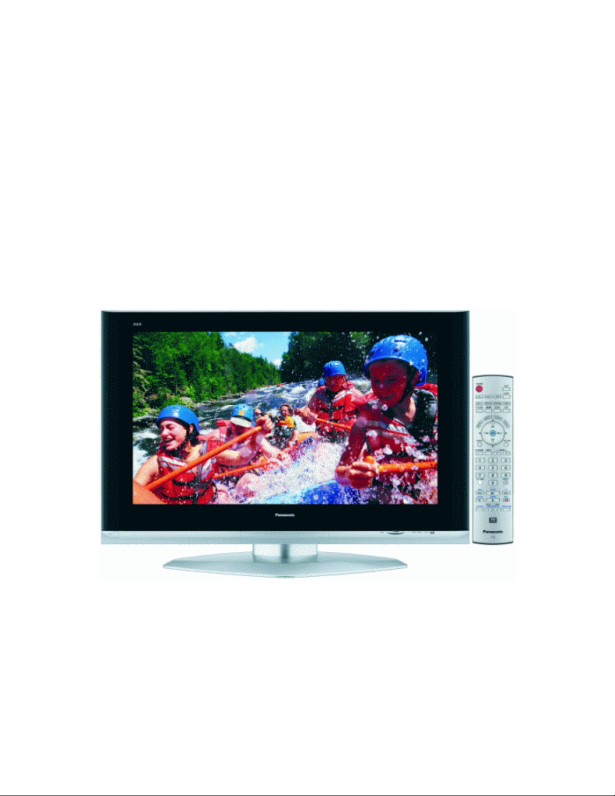
Panasonic GP8DU, GPH8DU Service Manual
Technical Guide
Plasma Training Course
TH-37PX50U, TH-42PD50U, TH-42PX50U,
TH-42PX500U, TH-50PX50U, TH-50PX500U
GP8DU and GPH8DU Chassis
Troubleshooting
Panasonic Services Company
National Training

A
y
Prepared by
Jean Magloire & Cesar Perdomo
Panasonic Services Company
National Training
"HDMI, the HDMI logo and High-Definition Multimedia Interface are trademarks or registered trademarks of HDMI Licensing LLC."
BBE, the BBE logo, Sonic Maximizer and High Definition Sound are registered trademarks or trademarks of BBE Sound, Inc.
Copyright © 2005 by Panasonic Services Company
ll rights reserved. Unauthorized copying and distribution is a violation of law.
Warning
This service information is designed for experienced repair technicians only and is not designed for use b
the general public. It does not contain warnings or cautions to advise non-technical individuals of potential
dangers in attempting to service a product. Products powered by electricity should be serviced or repaired
only by experienced professional technicians. Any attempt to service or repair the product or products
dealt with in this service information by anyone else could result in serious injury or death.

Table of Contents
Objective........................................................................................................................1
Specifications (Models Comparison) ..........................................................................2
Safety Precautions........................................................................................................3
TH-42PD50U Board Description and Part Numbers...................................................4
TH-42PX500U Board Description and Part Numbers................................................. 5
TH-50PX500 Board Description and Part Numbers....................................................6
Power Supply Outline for 42”and 50” Models ............................................................7
Standby Circuit.........................................................................................................8
Power On Operation ..............................................................................................12
Power Supply Connections........................................................................................ 15
P Board..................................................................................................................15
PA Board................................................................................................................ 16
PB Board................................................................................................................ 17
TH-42PX500U Block Diagram..................................................................................... 18
TH-42PX50U Block Diagram....................................................................................... 21
TH-42PD50U Block Diagram....................................................................................... 23
Video Input Selection Block Diagram........................................................................25
Audio Input Selection Block Diagram .......................................................................26
ATSC, SD and PC Card Input Signal Flow ................................................................27
DG Board Block Diagram ...........................................................................................28
Signal Process Circuit................................................................................................ 30
Main Picture Signal Flow........................................................................................30
Sub Picture Signal Flow.........................................................................................30
RGB Processor...................................................................................................... 31
D Board Block Diagram..............................................................................................32
C1 Board Block Diagram............................................................................................33
SC Board Explanation.................................................................................................34
SC board Waveform...............................................................................................35

SU And SD Board Shift Registers.......................................................................... 35
SS Board Explanation.................................................................................................37
SS Board Schematic..............................................................................................38
SS Board Waveform ..............................................................................................38
TH-42/50PX500U.......................................................................................................... 40
Power LED Flashing timing chart.............................................................................. 40
SOS Detection Circuits...............................................................................................41
SOS Detect (D Board)............................................................................................41
SOS Detect (DG Board).........................................................................................41
SOS Detect (D and PA Board)...............................................................................42
PA Board SOS Detection Circuits.............................................................................. 43
Over-Voltage Detection of Main Voltage (10 Blinks).............................................. 43
Short Circuit Detection of Main Voltage (10 Blinks)................................................44
Short Circuit Detection of Sub-voltage (10 Blinks) .................................................45
Other SOS Detection Circuits ....................................................................................46
SOS Detect (P, SC, and SS Board).......................................................................46
P Board SOS Detection .........................................................................................47
Voltage Distribution of the PA board and SOS Detection .......................................48
Z Board (Sound) SOS Detection ...............................................................................50
TH-42/50PX500U Self-check Function (Reset).......................................................... 51
Diagnostic Procedures...........................................................................................51
How to access the Self-check Screen (Reset).......................................................51
How to exit the Self-check Screen .........................................................................51
Screen Display......................................................................................................... 51
TH-42PD50U................................................................................................................. 53
Power LED Flashing timing chart.............................................................................. 53
TH-42/50PD50U Self-check Function.........................................................................54
Diagnostic Procedures...........................................................................................54
How to access the Self-check Screen (Reset).......................................................54
How to exit the Self-check Screen .........................................................................54
Screen Display......................................................................................................... 54
Serviceman Mode........................................................................................................ 56
How to enter the Serviceman Mode.......................................................................56
Adjustment method................................................................................................ 56
Cancellation ...........................................................................................................56

Contents of adjustment mode................................................................................56
Internal Pattern Generator .....................................................................................57
Cable Diagnostic Screen ............................................................................................57
Adjustments ................................................................................................................58
Driver Set-up.......................................................................................................... 58
Initialization Pulse Adjustment ...............................................................................59
Drive Waveform .......................................................................................................59
P.C.B. (Printed Circuit Board) exchange procedure ................................................60
Adjustment Volume Locations................................................................................... 61
Test Point Locations...................................................................................................62
Troubleshooting.......................................................................................................... 63
No Picture or Partial Picture...................................................................................63
Scan and Sustain Drive Waveform ........................................................................66
Scan and Sustain Drive Check points....................................................................66
Vertical line problems.............................................................................................71
Picture ok, Sound NG ............................................................................................72
No picture, no sound..............................................................................................73
No picture, sound ok.............................................................................................. 74
How to determine whether the D board or SC board is defective?.........................75
Additional Troubleshooting Hints............................................................................76
SC20 or D20 Connector........................................................................................... 77
How to determine whether the D board or SS board is defective?......................... 78
Defective Board .......................................................................................................79
Glossary and Acronyms.............................................................................................80

Objective
This technical guide was prepared with the following objectives in mind:
• Provide the servicer with a brief overview of the concepts of operation for new
circuits employed in this line of Plasma models
• Provide drawings with emphasis on signal path to simplify the task of signal tracing
and locate the cause of a defect
• Furnish troubleshooting procedures that contribute to a speedier repair of the
product
• Provide examples of typical problems that may have occurred in similar types of
circuits
1
Specifications (Models Comparison)
Features TH-42PD50U TH-42PX500 TH-50PX500
Resolution 852x480p 1024 x 768p 1366 x 768p
Altitude 2400m 2400m 2400m
Contrast 4000:1 3000:1 3000:1
Input Signal 720p 720p 720p
1080i 1080i 1080i
480p 480p 480p
480i 480i 480i
PC Input No Yes Yes
Input Terminal
(Video Input)
Video 1 S2/RCA (Rear) S2/RCA (Rear) S2/RCA (Rear)
Video 2 S2/RCA (Rear) S2/RCA (Rear) S2/RCA (Rear)
Video 3 No S2/RCA (Front) S2/RCA (Front)
Component 1 RCA (Rear) RCA (Rear) RCA (Rear)
Component 2 RCA (Rear) RCA (Rear) RCA (Rear)
PC Input
HDMI Input
Card Interface
Cable Card Slot
SD Card Slot No Yes Yes
PCMCIA Slot No Yes Yes
No Yes x 1 (Mini D-Sub
15 pin) (Rear)
Yes x 1 (Mini D-Sub
15 pin) (Rear)
Yes x 1 (Rear) Yes x 1 (Rear) Yes x 1 (Rear)
No Yes Yes
Table 1
2

Safety Precautions
Please follow these general guidelines before servicing the models mentioned in this
technical guide.
1. While servicing, please observe the original lead dress. If a short circuit is
found, replace all the parts that have been overheated or damaged by the
short circuit.
2. After servicing, please make sure that all the protective devices such as
insulation barriers, and insulation paper shields are properly installed.
3. Some semiconductor (solid state) devices can be easily damaged by static
electricity. Such components are commonly called Electrostatically Sensitive
(ES) devices. Examples of typical ES devices are integrated circuits, some
field-effect transistors (FET) and semiconductor "chip" components. The
following techniques should be used to help reduce the incidence of component
damage caused by Electro Static Discharge (ESD).
4. Drain off any Electro Static Discharge on your body by touching a known earth
ground, immediately before handling any semiconductor component or
semiconductor-equipped assembly. Alternatively, obtain and wear a
commercially available discharging ESD wrist strap, which should be
removed prior to applying power to the unit as it may cause an electric shock.
5. After removing an electrical assembly equipped with ES devices, place the
assembly on a conductive surface such as an aluminum foil, to prevent
electrostatic charge buildup or exposure on the assembly.
6. Use a grounded-tip soldering iron to solder or unsolder ES devices.
7. Use an anti-static solder removal device. Some solder removal devices not
classified as "anti-static (ESD protected)" can generate electrical charge
sufficient enough to damage an ES device.
8. Do not use freon-propelled chemicals. These can generate electrical charge
sufficient enough to damage an ES device.
9. Do not remove a replacement ES device from its protective package until you are
just ready to install it. (Most replacement ES devices are packaged with leads
electrically shorted together by conductive foam, aluminum foil or comparable
conductive material).
10. Immediately before removing the protective material from the leads of a
replacement ES device, touch the protective material to the chassis or the circuit
assembly into which the device will be installed.
Caution: Please make sure that no power is applied to the chassis or circuit
assembly, and observe all other safety precautions.
11. Minimize bodily motions when handling unpackaged replacement ES devices.
(Harmless motions such as the brushing together of your clothes fabric or the
lifting of your foot from a carpeted floor can generate static electricity sufficient
enough to damage an ES device).
3
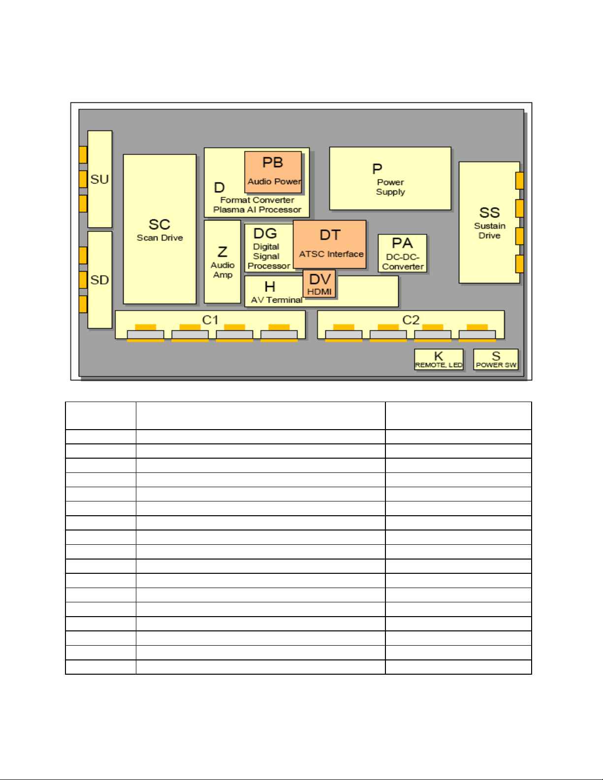
TH-42PD50U Board Description and Part Numbers
Board
Board Description Board Part Number
Name
P Power Supply TNPA3570
PA DC-DC Converter, Power SOS TNPA3620
PB Audio Power TNPA3643
H AV Terminal, AV Switch TNPA3598AB
DT ATSC Interface TNAG156
DV HDMI Interface TNPA3626
DG Digital Signal Processor TNPA3625AF
Z Speaker out, Audio AMP TNPA3621AB
D Format Converter, Plasma AI Processor TZTNP010YFS
C1 Data Driver (Left) TNPA3545
C2 Data Driver (Right) TNPA3546
SC Scan Drive TNPA3543
SU Scan out (Upper) TNPA3242
SD Scan out (Lower) TNPA3243
SS Sustain Drive TNPA3544
K Remote receiver, Keyscan TNPA3603
S Power Switch TNPA3604
Figure 1
Table 2
4
TH-42PX500U Board Description and Part Numbers
Board Name Board Description Board Part Number
P Power Supply ETXMM563MDK
PA DC-DC Converter, Power SOS TNPA3620
PB Audio Power, Fan control TNPA3643AD
H AV Terminal, AV Switch TNPA3598
DT ATSC Interface TNAG157S
DV HDMI Interface TNPA3626
DG Digital Signal Processor TNPA3625
Z Speaker out, Audio AMP TNPA3621
D Format Converter, Plasma Ai Processor TZTNP010YDS
K Remote receiver, OPT TNPA3498AB
S Power Switch TNPA3499AB
C1 Data Driver (Up Left) TNPA3553AB
C2 Data Driver (Up Right) TNPA3554
C3 Data Driver (Down Right) TNPA3555
C4 Data Driver (Down Left) TNPA3556
SC Scan Drive TNPA3557
SU Scan out (Up) TNPA3189AB
SD Scan out (Down) TNPA3190AB
SS Sustain Drive TNPA3558
SS2 Sustain Connector (Up) TNPA3675
SS3 Sustain Connector (Down) TNPA3676
G PC Card Slot, Front Terminal TNPA3496AF
GS SD Card Slot TNPA3497AF
GK Key Switch TNPA3503AB
Figure 2
Table 3
5
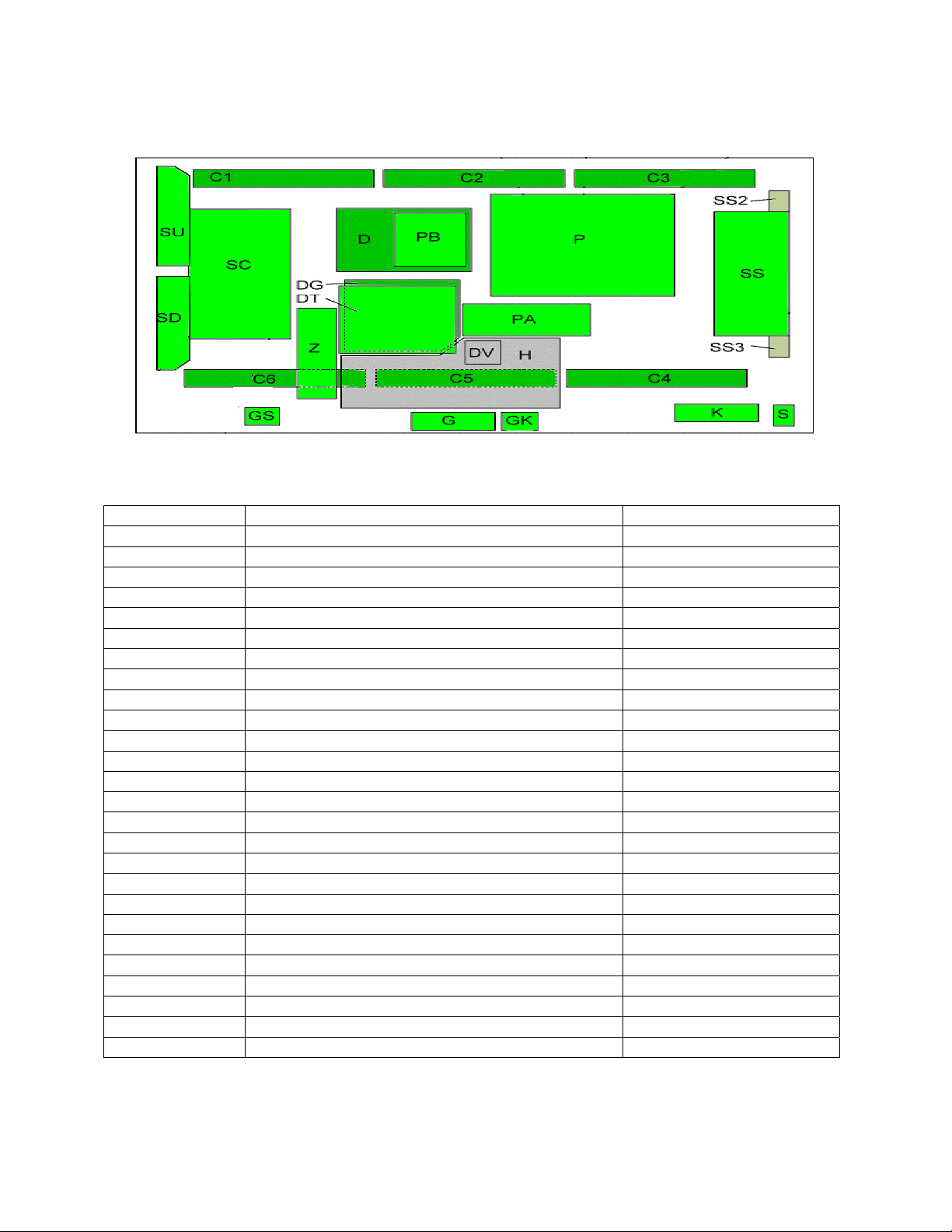
TH-50PX500 Board Description and Part Numbers
Board Name Board Description Board Part Number
DT ATSC Interface TNAG157S
H AV Terminal, AV Switch TNPA3598
PA DC-DC Converter, Power SOS TNPA3620
Z Speaker out, Audio AMP TNPA3621
DG Digital Signal Processor TNPA3625AB
DV HDMI Interface TNPA3626
PB Audio Power, Fan control TNPA3643AD
C1 Data Driver (Up Left) TNPA3561
C2 Data Driver (Up Center) TNPA3562
C3 Data Driver (Up Right) TNPA3563
C4 Data Driver (Down Right) TNPA3564
C5 Data Driver (Down Center) TNPA3565
C6 Data Driver (Down Left) TNPA3566
D Format Converter, Plasma AI Processor TZTNP010YCS
P Power Supply ETXMM564MEK
SC Scan Drive TNPA3567
SD Scan out (Down) TNPA3220AB
SS2 Sustain Connector (Up) TNPA3559
SS Sustain Drive TNPA3568
SS3 Sustain Connector (Down) TNPA3560
SU Scan out (Up) TNPA3219AB
K Remote receiver, OPT TNPA3498AB
GS SD Card Slot TNPA3497AF
G PC Card Slot, Front Terminal TNPA3496AF
GK Key Switch TNPA3503AB
S Power Switch TNPA3499AB
Figure 3
Table 4
6
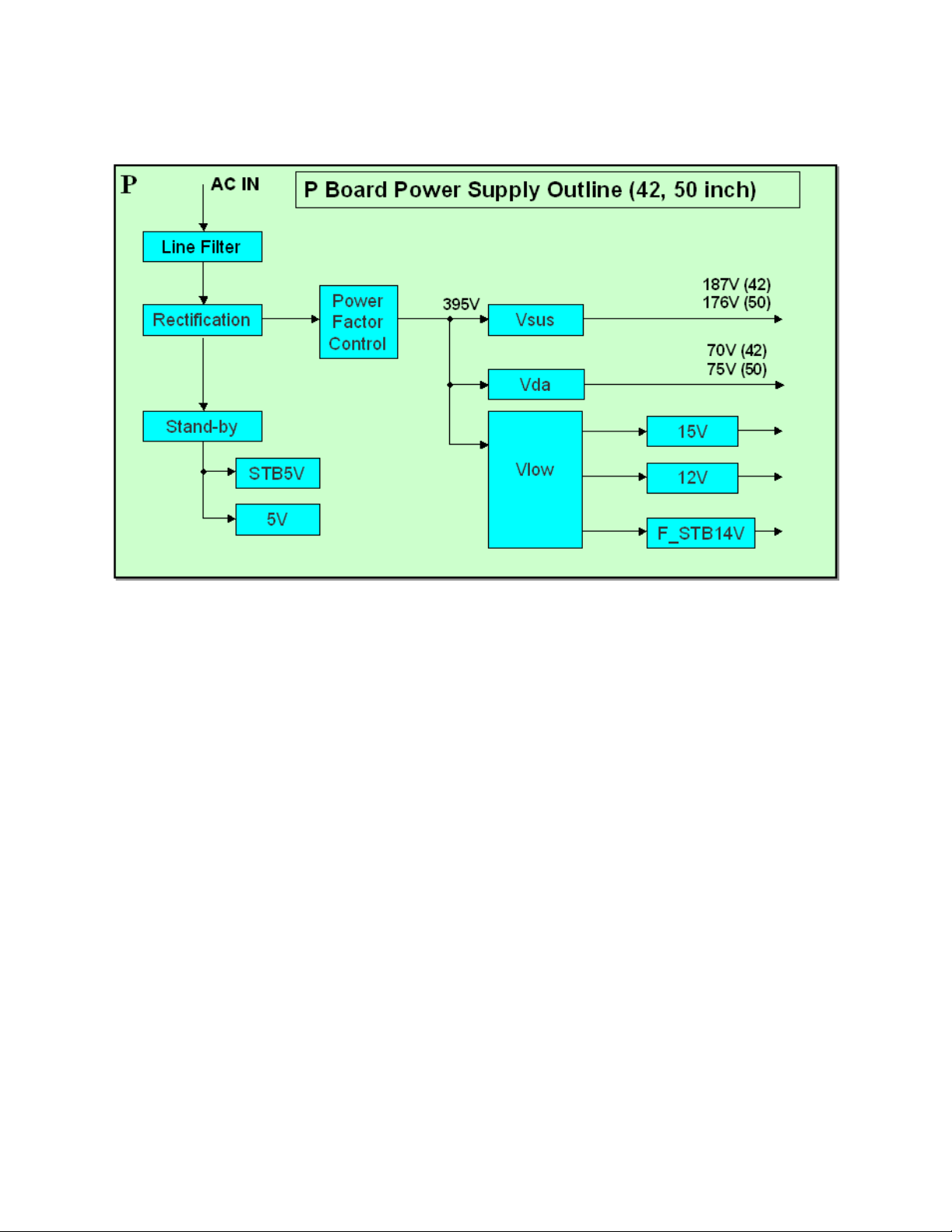
Power Supply Outline for 42”and 50” Models
The PF board of the older Plasma Television models is now incorporated into the P
board of the GPH8DU chassis.
The function of the line filter is to block incoming noise from the AC outlet to the unit and
outgoing noise from the unit to the AC outlet. The basic operation of the new P board is
the same as that of the older Plasma Display Televisions.
The Standby circuit supplies STB5V and 5V for FAN SOS. The main circuit supplies
Vsus voltage for sustain and scan operations, Vda voltage for data drive (C boards),
15V for sustain, scan, and fan operations, and 12V for audio power. The F_STB14V is
used on the PA board to generate other operating voltages.
Figure 4
7
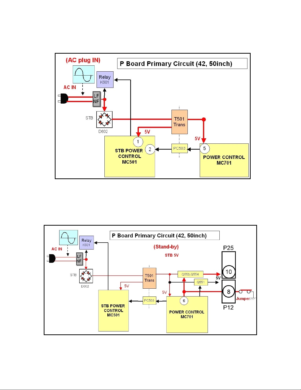
Standby Circuit
Figure 5
The diode D602 and the transformer T501 are used to develop the STB5V supply.
The STB5V is applied to pin 5 of the Power control IC MC701 and pin 1 of the Power
Control IC MC501 (Use hot ground to measure voltage on MC501). (See Fig. 5.)
Figure 6
8
Instead of a standby power switch, as it shows in the diagram, the TV has a jumper wire
on the “S” board that connects pin 8 of the connector P12 to ground. As a result the
transistors Q553 and Q554 turn on, allowing the STB5V to be applied to the D and the
DG-board via pin 10 of the connector P25. (See Fig. 6).
Figure 7
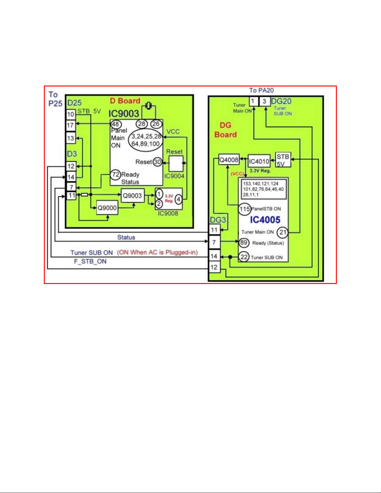
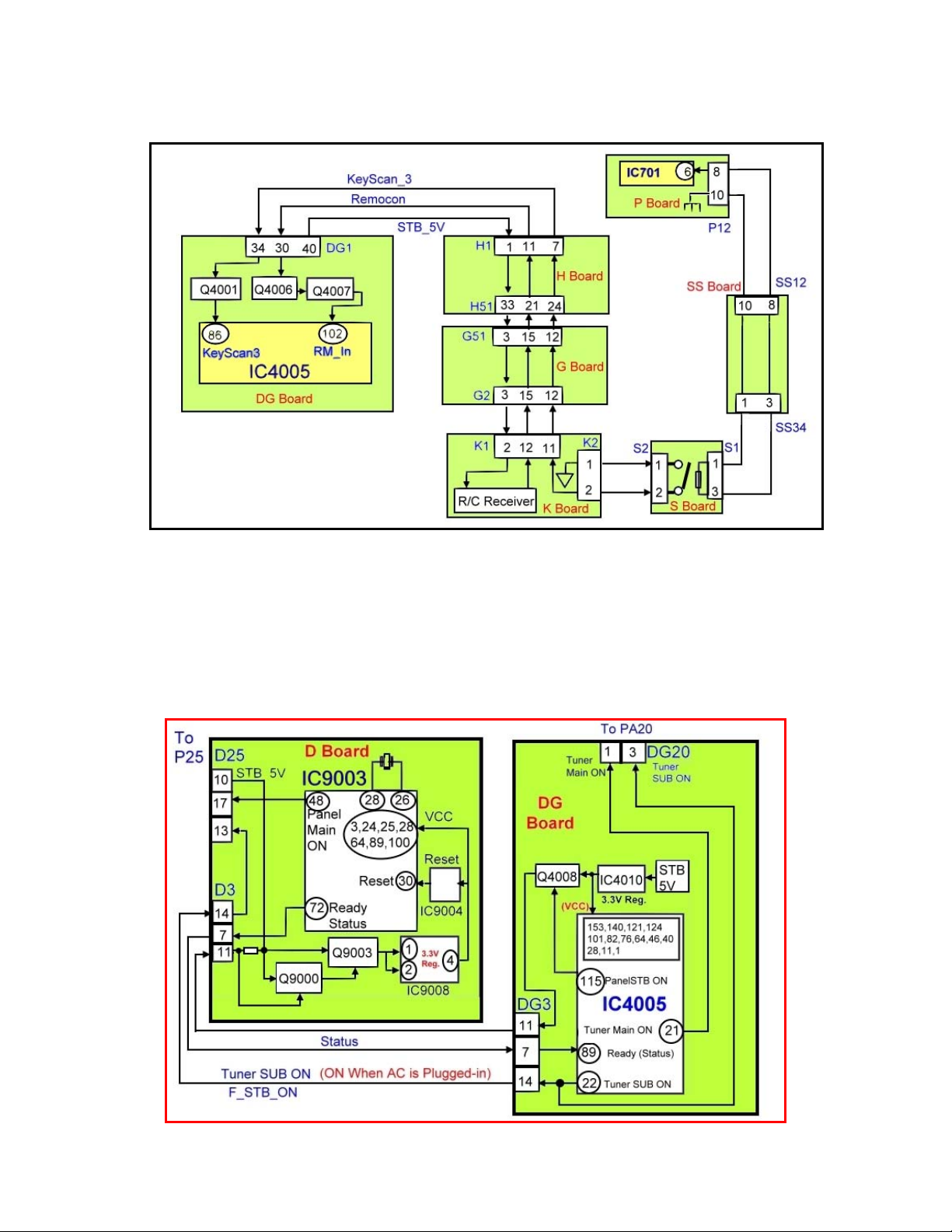
The Microprocessor on the DG board (IC4005) receives the regulated STB3.3V from
IC4010. Pin 22 of IC4005 outputs 2.5V (Tuner SUB ON) to the P board via pin 14 of the
connectors DG3/D3 and pin 13 of the connector P25/D25. It is then connected to pin 21
(F. STB ON) of the “Power Output Control” IC, MC701. (See Fig. 7 & 8.)
9
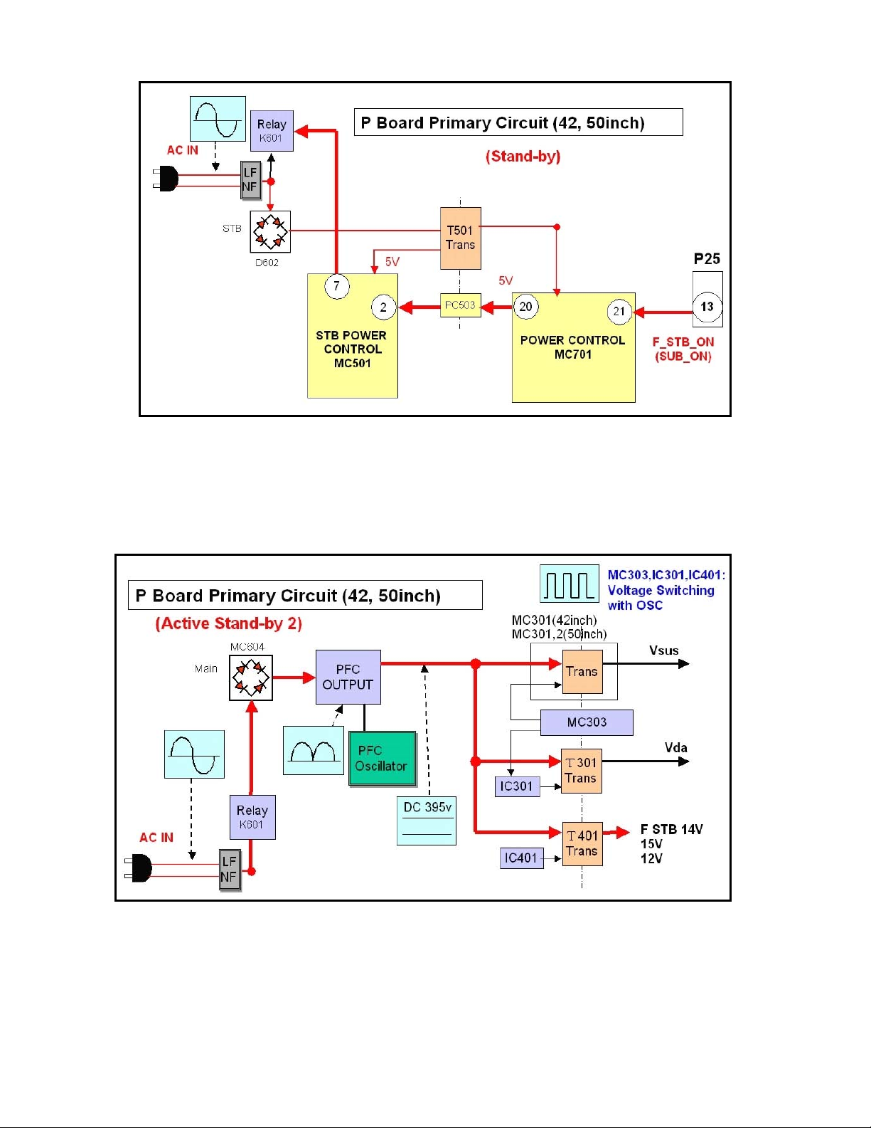
Figure 8
The power control IC, MC701, upon receiving the “F.STB ON” voltage, outputs the “PC
PFC ON” control signal at pin 20. This turns on the photocoupler PC503 to provide a
low to pin 2 of the “STB Power Control” IC, MC501. MC501 outputs the “relay ON”
control signal to activate the relay K601. (See Fig. 8)
Figure 9
The rectifier MC604 rectifies the 120VAC from the relay and outputs to the “PFC
Control” MC602.
10
The DC voltage from the rectifier is converted to 395Vdc by the “Power Factor
Control” circuit to improve the power ratio.
This DC voltage is applied to three different circuits; the Vsus, the Vda and the Low
Voltage (F STB 14V, 15V, and 12V) power supplies.
During standby operation, both the Vsus and the Vda power supply circuits are off.
Only the “F STB 14V” section of the Low Voltage power supply circuit is on.
Figure 10
The “F14V ON” command (5V) from pin 10 of MC701 turns on Q452 and the “F STB
14V” is output to the PA-board through pins 1, 2, and 3 of connector P10.
(See Fig. 10)
Note: The above description is true for standby mode only; the power has not been
turned on yet.
11
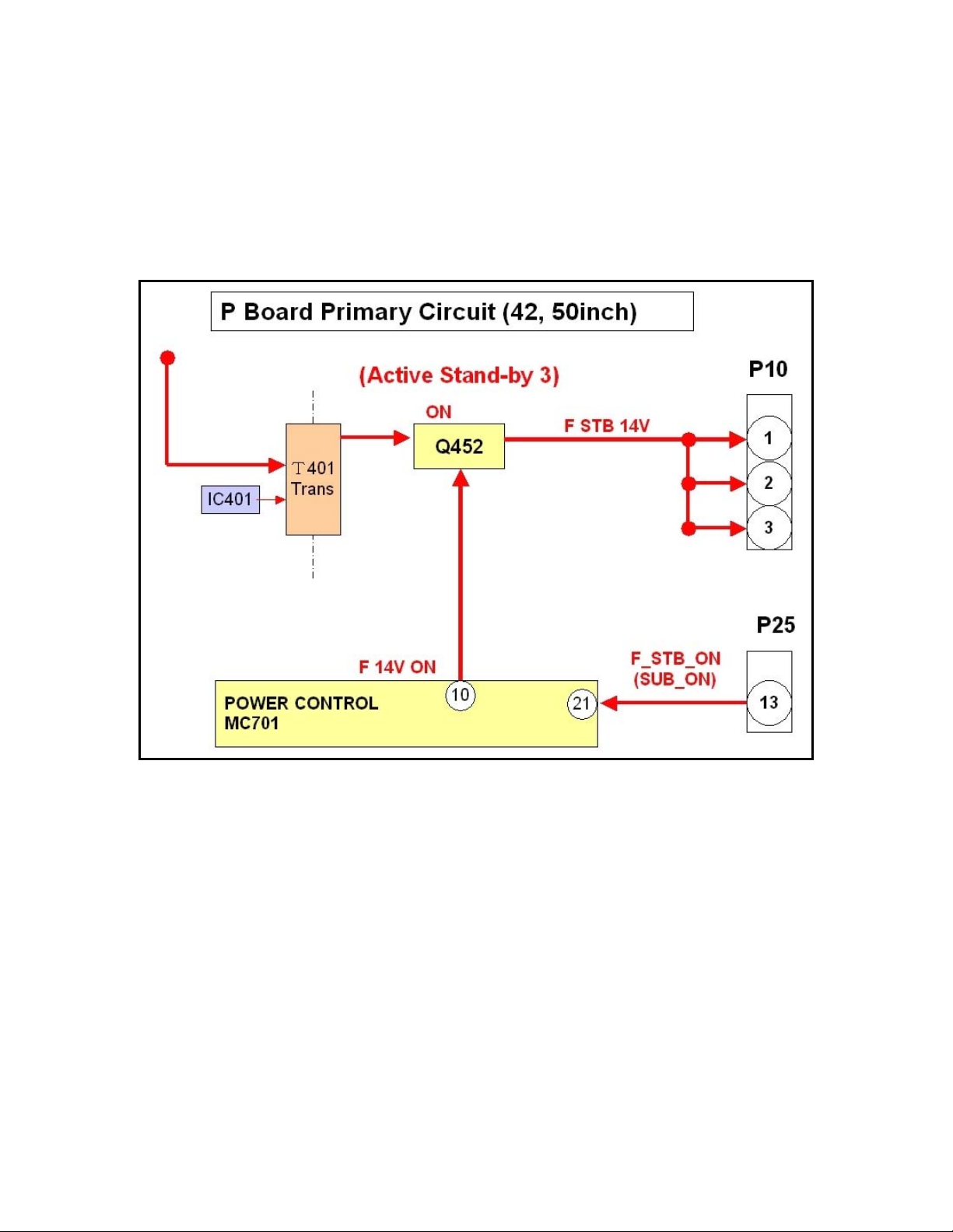
Power On Operation
The momentary connection of the power switch to ground supplies a low to the base of
Q4001 (DG board) to turn it on. When Q4001 is on, a low is provided to pin 86 (Key
scan 3) of the microprocessor IC4005.
he R/C receiver receives the power on command of the remote control and outputs the
T
IR data to the amplifiers Q4006 and Q4007 of the DG board. The data is amplified and
output to pin 102 of the MPU, IC4005.
Figure 11
Figure 12
12
Upon receiving the power on command, pin 21 of IC4005 (Tuner Main ON) goes high
and pin 115 (Panel STB ON) goes low.
Pin 21 is connected to pin 28 of the connector PA20 via pin 1 of the connector DG20.
The high at pin 21 is the control signal used to turn on the circuit that generates the
SUB 3.3V, the Main 3.3V, the Main 5V, and the Main 9V sources of the PA board.
The low from pin 115 is connected to the base of Q4008 located on the DG board. It
causes Q4008 to stop conducting, and output a High to the base of Q9000 on the D
board, thus turning it on. When Q9000 is on, the collector goes low. This low is applied
to the gate of Q9003 turning it on to provide 5V to pins 1 and 2 of IC9008 (3.3V Reg.).
The 3.3V out of pin 4 of IC9008 is connected to the VCC pins 3, 24, 25, 28, 64, 89, and
100 of the microprocessor IC9003. The 3.3V is also connected to the reset circuit
IC9004.
When IC9003 receives the 3.3V, it does a reset and outputs a high at pin 48 (Main
Panel ON). (See Fig. 12). This voltage is provided to pin 17 of the connector P25.
Figure 13
13

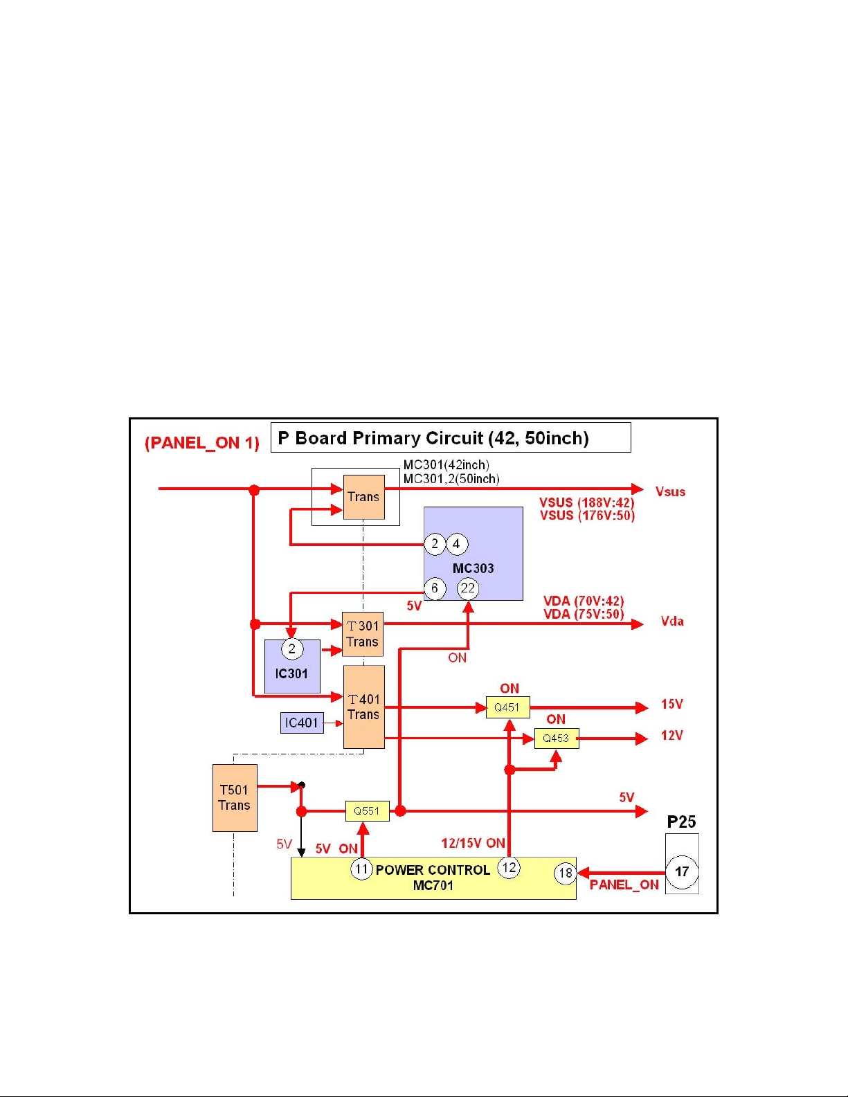
The high command at pin 17 of connector P25 is applied to pin 18 of MC701 of the P
board. Pin 11 switches from 5V to 1.3V, and pin 12 from 15V to 0V.
The 1.3V at pin 11 causes Q551 to turn on and output 5V. The 5V is applied to pin 22 of
the “Drive Voltage Oscillator” MC303. It is also applied to the “Fan SOS” circuit of the
PB board via pin 4 of the connector P30. (See Fig 14.)
The 5V on pin 22 of IC MC303 causes it to operate. IC MC303 then turns on the Vsus
power supply circuit (MC301) and the Vda power supply circuit (IC301, and T301).
Vsus is output to SC and SS-boards. Vda is output to the Data Drive Circuit boards via
the SC board.
The low from pin 12 is used to turn on Q453, and Q451.
When Q453 is on, it outputs 12V to the PB board and the D board.
When Q451 is on, it outputs 15V to the PB board and the SC board
14
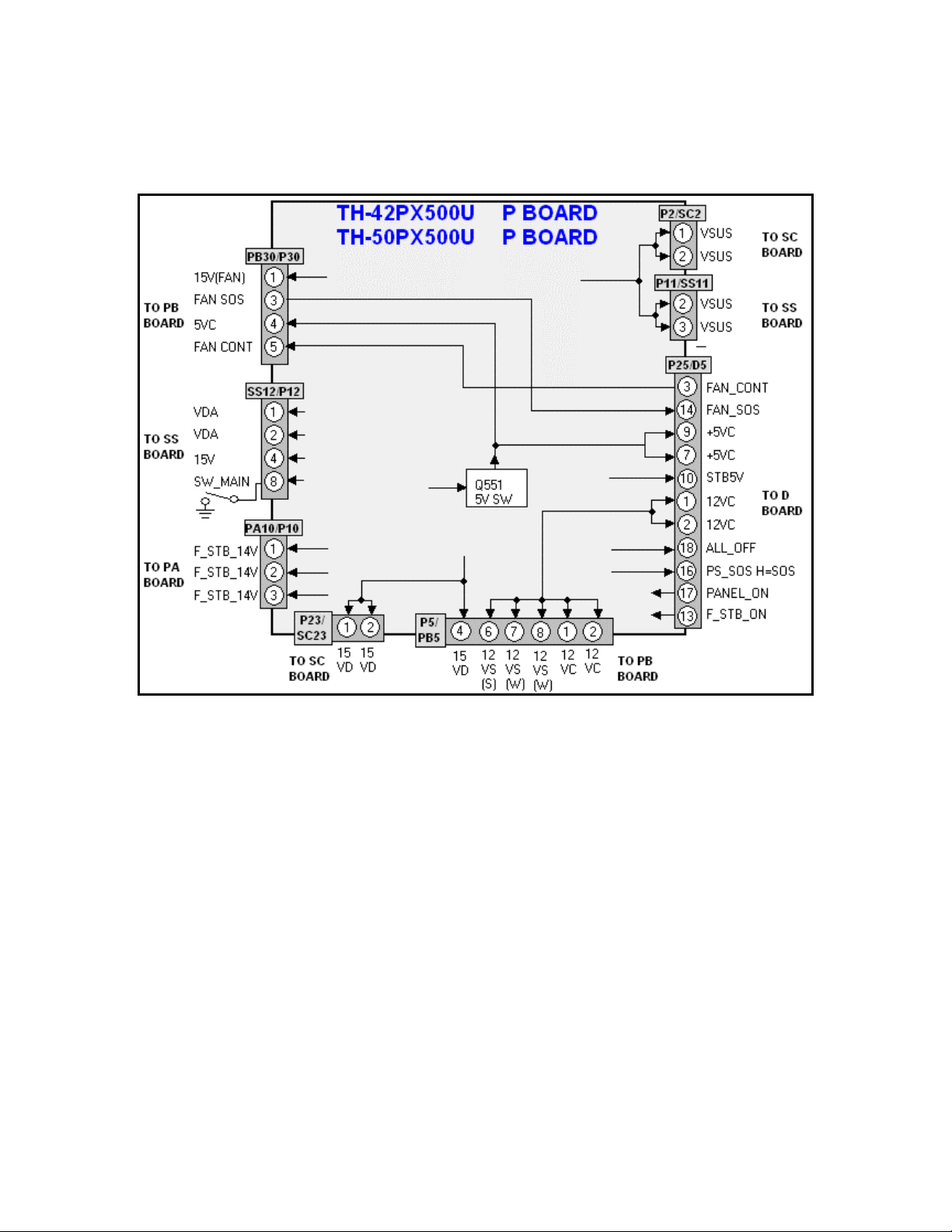
Power Supply Connections
P Board
The P board houses the main power supply of the unit. All voltages originate from this
board. The connector information is to be used for troubleshooting purposes.
Figure 14
15
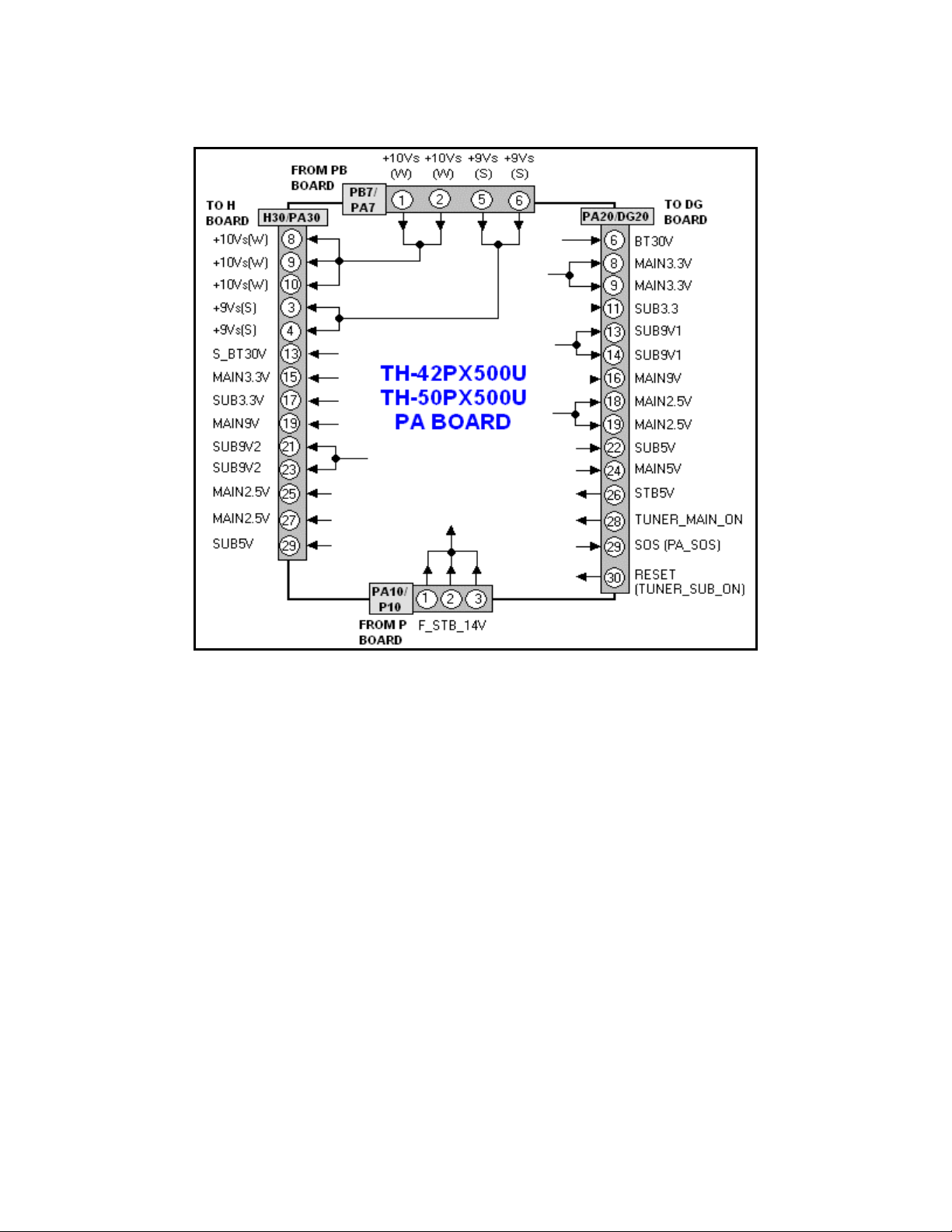
PA Board
The PB board utilizes voltages obtained from the P board to create lower and higher
voltages for use in different sections of the unit. The connector information can prove
useful when troubleshooting.
Figure 15
16
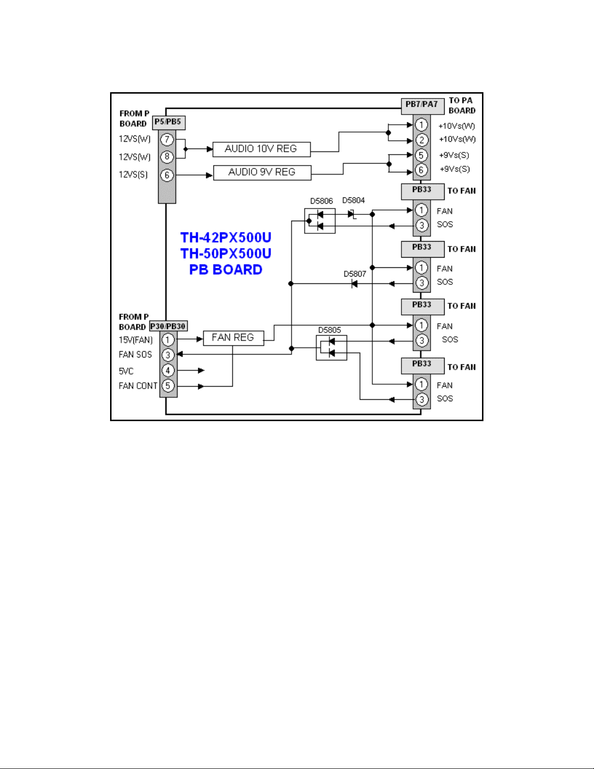
PB Board
The PB board contains voltage regulators that power the Audio circuit (Z board) and the
fans. The connector information is to be used for troubleshooting purposes.
Figure 16
17
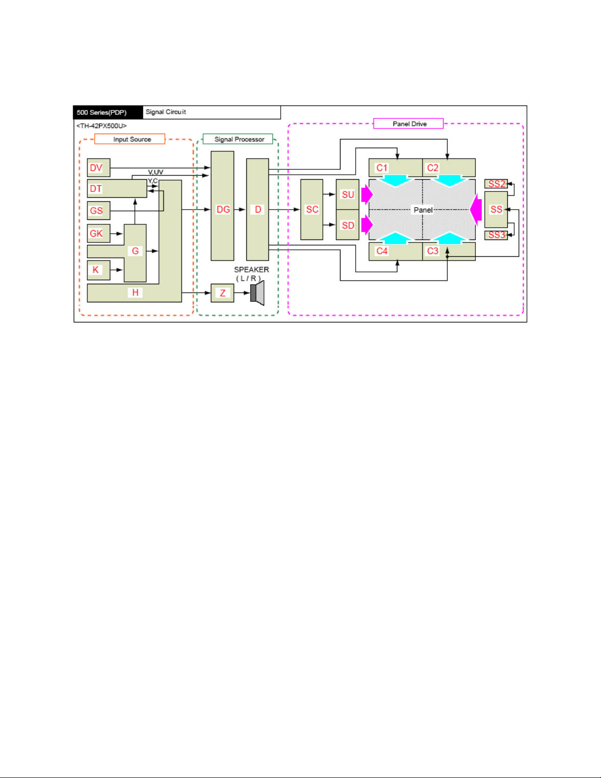
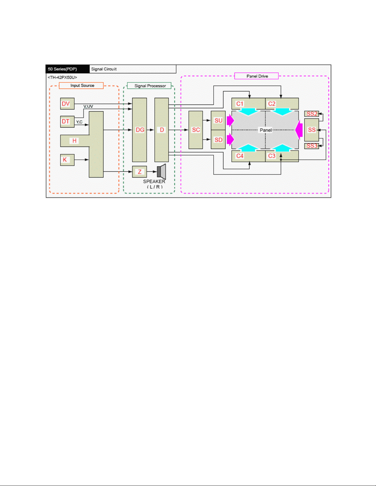
TH-42PX500U Block Diagram
The DV board processes HDMI or DVI input signals. The HDMI IF receiver converts the
digital signal into parallel Y, U, V data and outputs it to the DG board for video selection
and processing.
GP8HD series plasma panels incorporate a Set Top Box that is designed to receive
NTSC and ATSC television broadcast. It is also used to receive QAM cable television
transmission. It is a hybrid tuner that processes NTSC and ATSC terrestrial broadcast
for reproduction on the TV screen.
The DT-Board also incorporates the OpenCable interface for use with a CableCard.
This tuner allows the reception of Digital Cable television without the use of a set-topbox.
The DT board contains an Optical Audio Out jack for use with a Dolby Digital decoder
and a multi-channel amplifier. When a digital channel is selected, the output from the
Digital Audio Out jack is Dolby Digital. The same jack outputs PCM (Pulse Code
Modulation) when any other signal source is selected.
An SD card slot is also included in the DT board. As the OpenCable service changes,
the firmware information located in the DT board may be upgraded by using an SD
card.
The DT board contains the host identification number and stores the identification
number of the CableCard.
Figure 17
18

It also processes the JPEG data of the SD and PC cards used for viewing pictures.
Photo-viewer data from the G and GS boards are input to the DT board and converted
to analog luminance and chrominance signals. Analog Television and Photo-viewer
signals are output to the H board and selected like any other source. Digital television
signals (Y, Pb, Pr) are output to the DG board for video selection and processing.
The GS board contains the SD card slot that is used for Photo-viewing. The digital
output signal passes through the H board and enters the DT board for processing.
The GK is the operation board of the unit. The key scan pulses are routed to the DG
board MPU via the G and H boards.
The G board contains one of the video inputs and the PC card slot, which is used for
viewing photos. The digital output signal of the PC card passes through the H board and
enters the DT board for selection and processing. The analog video input signal is
provided to the H board for selection among many other video inputs.
The K board contains the optical sensor used for CATS (Contrast Automatic Tracking
System). It also contains the Remote IR sensor and the power LED.
The unit also contains two other video inputs, two component inputs, and a PC input
(depending upon the model) that are directly connected to the main switch of the H
board.
The H board selects and outputs, to the DG board, the main video and sub video
signals for display on the screen.
The DG board is responsible for the complete video processing within the unit. All
analog inputs to the DG board are immediately converted to digital. All signal
processing in the DG board is performed digitally. Signals from a digital TV or HDMI
source are provided to the DG board in digital form. The board performs PIP (Picture in
Picture) and picture control operations such as brightness, contrast, color, tint, etc. The
board also performs pixel conversion to change the resolution of the picture to the
resolution of the screen. The output signal of the board passes through an LVDS (Low
Voltage Differential Signaling) transmitter for conversion into serial data. The PEAKS
firmware of the unit also resides in this board.
The D board is responsible for displaying the picture on the screen. It provides the scan,
sustain and data drive signals. The scan pulses are output to the SC board. The sustain
pulses are output to the SS board. The data drive signals are output to the C1, C2, C3
and C4 boards. The C1 board drives the upper right portion of the panel; the C2 board
drives the upper left portion. The C3 and C4 boards drive the lower right and left
portions of the panel respectively.
The SC board is responsible for the generation of the scan pulses. Scan pulses are
used for initialization and selection of the pixels.
19

The SU and SD boards are demultiplexer boards that are responsible for converting
serial data output of the SC board into parallel data to drive the panel.
The SS board is responsible for the generation of the sustain pulses. Sustain pulses are
used to initialize and control the brightness of the screen.
The SS2 and SS3 boards are extension (connector) boards used to connect the SC
board to the panel.
20
TH-42PX50U Block Diagram
The DV board processes HDMI or DVI input signals. The HDMI IF receiver converts the
digital signal into parallel Y, U, V data and outputs it to the DG board for video selection
and processing.
GP8HD series plasma panels incorporate a Set Top Box that is designed to receive
NTSC and ATSC television broadcast. It is also used to receive QAM cable television
transmission. It is a hybrid tuner that processes NTSC and ATSC terrestrial broadcast
for reproduction on the TV screen.
The DT-Board also incorporates the OpenCable interface for use with a Cable Card.
This tuner allows the reception of Digital Cable television without the use of a set-topbox.
The DT board contains an Optical Audio Out jack for use with a Dolby Digital decoder
and a multi-channel amplifier. When a digital channel is selected, the output from the
Digital Audio Out jack is Dolby Digital. The same jack outputs PCM (Pulse Code
Modulation) when any other signal source is selected.
An SD card slot is also included in the DT board. As the OpenCable service changes,
the firmware information located in the DT board may be upgraded by using an SD
card.
The DT board contains the host identification number and stores the identification
number of the CableCard.
Figure 18
21
 Loading...