

Page 1
ORDER NO. EXP0403007C2
Digital Progressi ve Plasma Television
TH-37PE30B
TH-42PE30B
GP6DE Chassis
Specifications
Power Source 220 V -240 V 50 Hz /60 Hz A.C.
Power Consumption
Normal use 253 W (TH-37PE30B), 323 W (TH-42PE30B)
Standby 1.8 W (TV only), 15.0 W (TV + DVB system set to record Timer programmes)
Power-OFF 1.0 W
Plasma Displ ay panel
Drive method AC type
Aspect Ratio 16:9
Contrast Ratio 4000:1
Screen size (No.of pixels) 37-inch (TH-37PE30B)
818 mm (W) × 461 mm (H) × 939 mm (diagonal)
42-inch (TH-42PE30B)
920 mm (W) × 518 mm (H) × 1,056 mm (diagonal)
408,960 (852 (W) × 480 (H)) [2,556 × 480 dots ]
Sound
Speaker Woofer 80 mm × 2, Tweeter 16 mm × 73 mm × 8
Audio Output 26W[8W+8W,5W+5W]((10%THD)
Headphone M3 (3.5 mm) Jack × 1
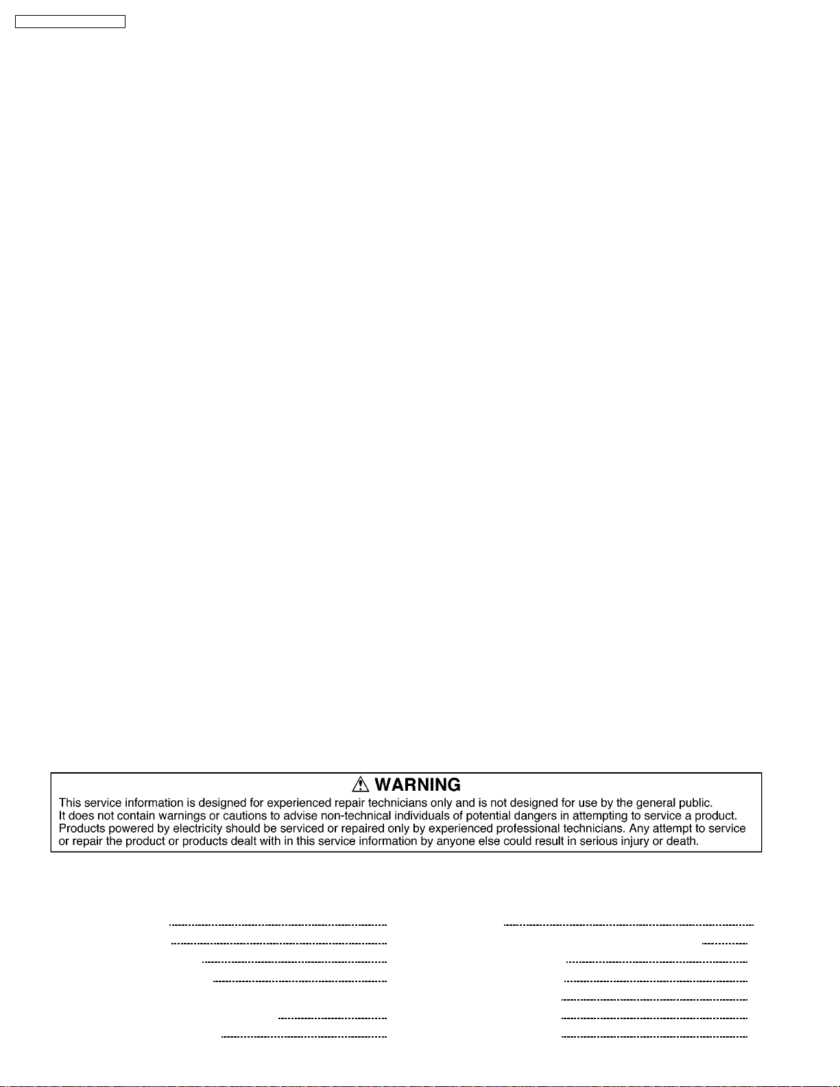
Applicable signals
Colour System NTSC, PAL, PAL60, SECAM, Modified NTSC
Scanning format 525 (480) /60i 60p, 625 (575) /50i 50p
PC signals VGA display
VGA
SVGA, XGA, SXGA, UXGA ..... (compressed)
Horizontal scanning frequency 15 - 110 kHz
Vertical scanning frequency 48 - 120 Hz
Receiving Systems/Band namePAL I
UHF E21 - 68.
© 2004 Matsushita Electric Industrial Co., Ltd. All
rights reserved. Unauthorized copying and
distribution is a violation of law.
Page 2
TH-37PE30B / TH-42PE30B
OUTPUT
AUDIO OUT AUDIO L-R (RCA Pin Type × 2) 0.5 Vrms
INPUT
AV3-Front VIDEO (RCA Pin Type × 2) 1.0 Vp-p (75 9)
AV4C-Rear Y 1.0 Vp-p (including synchronization)
PC (HIGH-DENSITY D-SUB 15PIN) R, G, B/ 0.7 Vp-p (75 9)
Others SD Card slot × 1, PC Card slot × 1
INPUT/OUTPUT
AV1-Rear 21 Pin terminal (Audio/Video in, TV out, RGB in)
AV2-Rear 21 Pin terminal (Audio/Video in, Audio/Video out, S-Video in, Q-Link)
AV4-Rear 21 Pin terminal (Audio/Video in, Audio/Video out, S-Video in, RGB in, Q-Link)
ANT-Rear UHF / VHF
Operating Conditions Temperature :0 ° - 40 °C
Accessories Supplied
Operating Instructions TQBC0719-1
Mains Lead K2CT3DH00017
Remote Control Transmitter EUR7635010
Batteries 2×R6Size
Clamper TMME206 × 2
Ferrite core Large size × 2, Small size × 5
Dimensions ( W × H × D ) 1,040 mm × 697 mm × 139 mm (TH-37PE30B)
Mass (Weight) 34.5 kg (TH-37PE30B)
PAL 525/60 Playback of NTSC tape from some PAL Video recorders (VCR)
DVB Digital terrestrial services via UHF aerial input.
M.NTSC Playback from M.NTSC Video recorders (VCR)
NTSC (AV INPUT ONLY) Playback from NTSC Video recorders (VCR)
S-VIDEO (MINI DIN 4-pin) Y: 1.0 Vp-p (75 9 ) C:0.286 Vp-p (75 9)
AUDIO L-R (RCA Pin Type × 2) 0.5 Vrms
PB/P
R
Humidity :20 % - 80 %RH (non-condensing)
1,140 mm × 757 mm × 139 mm (TH-42PE30B)
41.0 kg (TH-42PE30B)
±0.35 Vp-p
HD, VD / 1.0 - 5.0 Vp-p (high impedance)
Notes:
·
· Design and specifications are subject to change without notice.Mass and dimensions shown are approximate.
· ·
·
· This equipment complies with the EMC standards listed below.
· ·
EN55013,EN61000-3-2,EN61000-3-3,EN55020.
CONTENTS
1 Applicable signals 5
2 Safety Precautions
2.1. General Guidelines
2.2. Touch-Current Check
3 Prevention of Electro Static Discharge (ESD) to
Electrostatically Sensitive (ES) Devices
4 About lead free solder (PbF)
Page Page
5 Service Hint
6 P.C.Board and Plasma panel replacement method
6
6
7 Location of Lead Wiring
6
7
8
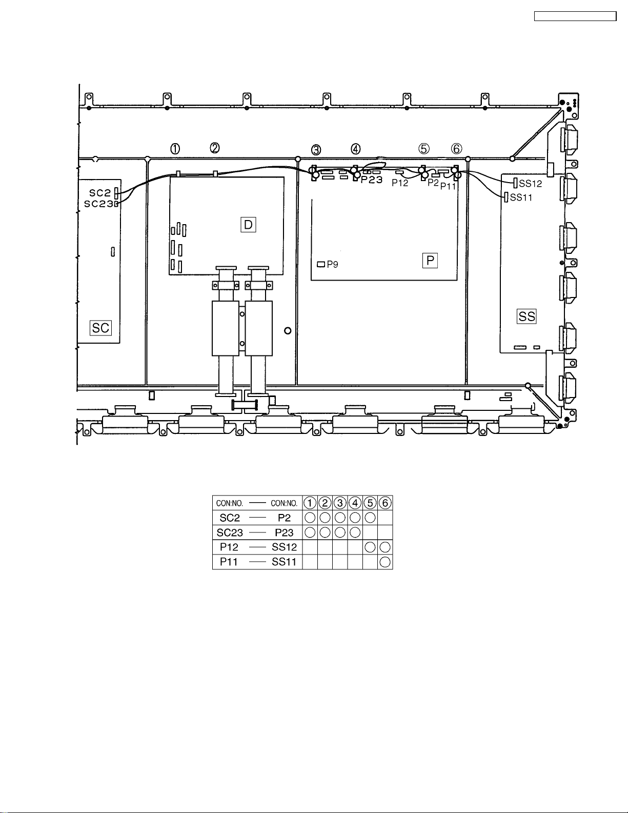
7.1. Lead of Wiring (1)
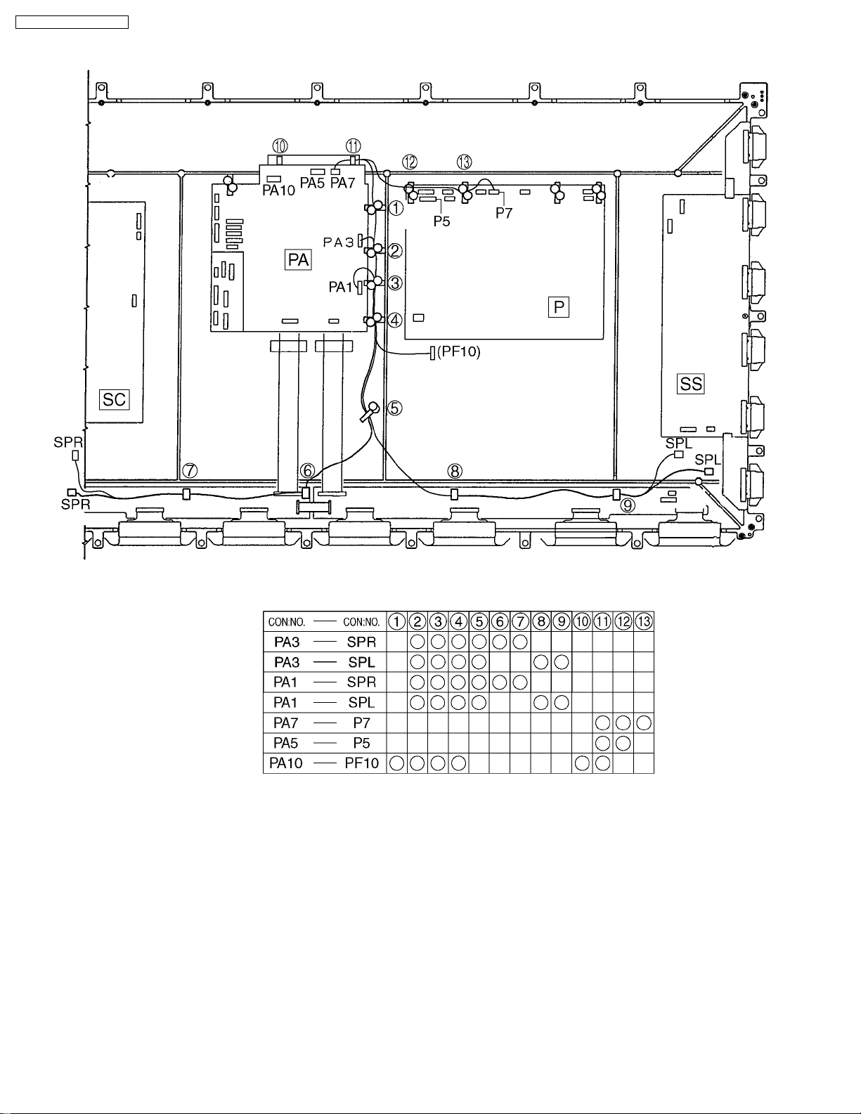
7.2. Lead of wiring (2)
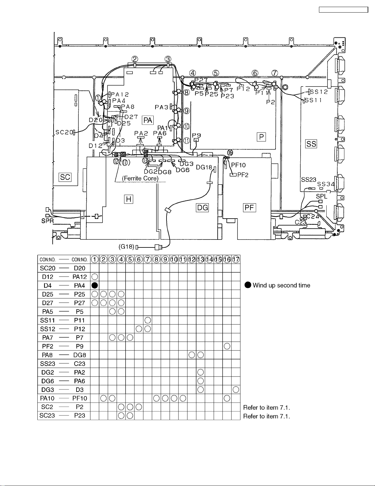
7.3. Lead of wiring (3)
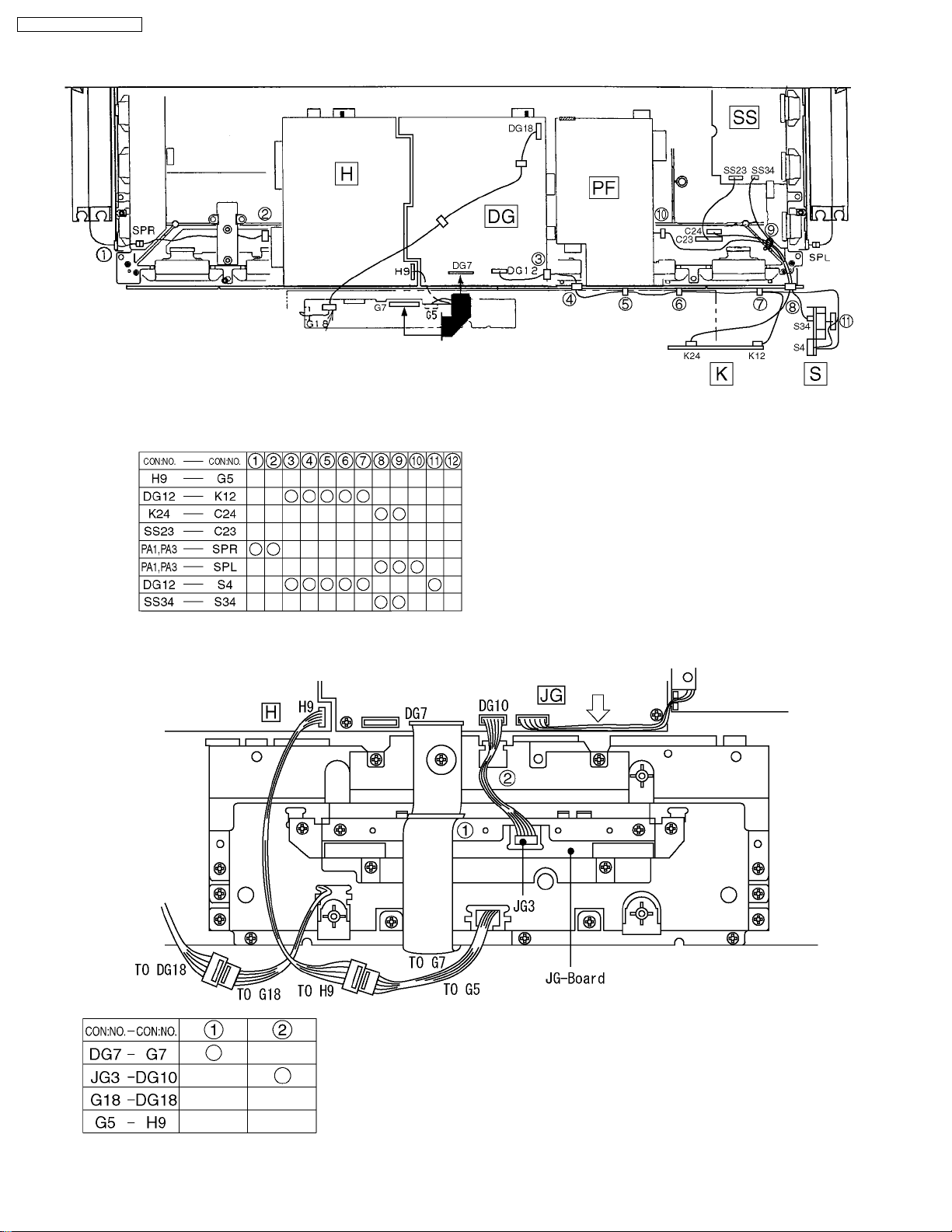
7.4. Lead of wiring (4)
10
15
15
16
17
18
2
9
Page 3

7.5. Lead of wiring (5) 18
7.6. Lead of wiring (7)
8SelfCheck
8.1. Power LED Blinking timing chart
8.2. No Power
8.3. No Picture
8.4. Local screen failure
9 Service Mode Function
9.1. How to enter SERVICE 1
9.2. How to enter SERVICE 2
9.3. Option Description
10 CAT (Computer Aided Test) mode
10.1. IIC mode
10.2. CD mode
10.3. SD mode
10.4. IIC mode structure (following items value is sample data.)
11 Adjustment Procedure
11.1. +B Set-up
11.2. Driver Set-up
11.3. Initialization Pulse Adjust
11.4. P.C.B. (Printed Circuit Board) exchange
11.5. Adjustment Volume Location
11.6. Test Point Location
12 Alignment
12.1. Pedestal setting
12.2. PAL panel white balance
12.3. PC panel white balance
12.4. Sub brightness setting
12.5. ABL Level
13 Hotel mode
14 Conductor Views
14.1. PF-Board
14.2. P-Board
14.3. PA-Board
14.4. D-Board
14.5. DG-Board
14.6. H and T-Board
14.7. C1-Board (For TH-37PE30B)
14.8. C1-Board (For TH-42PE30B)
14.9. C2-Board (For TH-37PE30B)
14.10. C2-Board (For TH-42PE30B)
14.11. SC-Board
14.12. SU-Board (For TH-37PE30B)
14.13. SU-Board (For TH-42PE30B)
14.14. SD-Board (For TH-37PE30B)
14.15. SD-Board (For TH-42PE30B)
14.16. SS-Board
14.17. SS2, SS3, SS4 and SS5-Board
14.18. K and S-Board
14.19. G-Board
14.20. JG-Board
14.21. XV-Board
15 Block and Schematic Diagrams
19
20
21
22
23
23
24
24
24
26
28
28
29
29
30
31
31
31
32
33
33
33
34
34
35
36
37
37
38
39
39
41
43
45
47
49
51
52
53
54
55
58
59
60
61
62
64
65
66
67
69
71
TH-37PE30B / TH-42PE30B
15.1. Schematic Diagram Notes
15.2. Main Block Diagram
15.3. PF-Board Block Diagram
15.4. PF-Board Schematic Diagram
15.5. P-Board Block Diagram
15.6. P-Board Schematic Diagram
15.7. PA-Board Block Diagram
15.8. PA-Board (1 of 2) Schematic Diagram
15.9. PA-Board (2 of 2) Schematic Diagram
15.10. H and T-Board Block Diagram
15.11. H-Board (1 of 2) Schematic Diagram
15.12. H-Board (2 of 2) and T-Board Schematic Diagram
15.13. DG-Board (1 of 2) Block Diagram
15.14. DG-Board (2 of 2) Block Diagram
15.15. DG-Board (1 of 9) Schematic Diagram
15.16. DG-Board (2 of 9) Schematic Diagram
15.17. DG-Board (3 of 9) Schematic Diagram
15.18. DG-Board (4 of 9) Schematic Diagram
15.19. DG-Board (5 of 9) Schematic Diagram
15.20. DG-Board (6 of 9) Schematic Diagram
15.21. DG-Board (7 of 9) Schematic Diagram
15.22. DG-Board (8 of 9) Schematic Diagram
15.23. DG-Board (9 of 9) Schematic Diagram
15.24. D-Board Block Diagram
15.25. D-Board (1 of 12) Schematic Diagram
15.26. D-Board (2 of 12) Schematic Diagram
15.27. D-Board (3 of 12) Schematic Diagram
15.28. D-Board (4 of 12) Schematic Diagram
15.29. D-Board (5 of 12) Schematic Diagram
15.30. D-Board (6 of 12) Schematic Diagram
15.31. D-Board (7 of 12) Schematic Diagram
15.32. D-Board (8 of 12) Schematic Diagram
15.33. D-Board (9 of 12) Schematic Diagram
15.34. D-Board (10 of 12) Schematic Diagram
15.35. D-Board (11 of 12) Schematic Diagram
15.36. D-Board (12 of 12) Schematic Diagram
15.37. C1, C2, G and K-Board Block Diagram
15.38. C1-Board Schematic Diagram (TH-37PE30B)
15.39. C1-Board Schematic Diagram (TH-42PE30B)
15.40. C2-Board (1 of 2) Schematic Diagram (TH-37PE30B)
15.41. C2-Board (2 of 2) Schematic Diagram (TH-37PE30B)
15.42. C2-Board Schematic Diagram (TH-42PE30B)
15.43. G-Board Schematic Diagram
15.44. K-Board Schematic Diagram
15.45. SC-Board Block Diagram
15.46. SC-Board (1 of 3) Schematic Diagram
15.47. SC-Board (2 of 3) Schematic Diagram
15.48. SC-Board (3 of 3) Schematic Diagram
15.49. SU-Board Block Diagram
15.50. SU-Board Schematic Diagram (TH-37PE30B)
15.51. SU-Board Schematic Diagram (TH-42PE30B)
15.52. SD-Board Block Diagram
15.53. SD-Board Schematic Diagram (TH-37PE30B)
15.54. SD-Board Schematic Diagram (TH-42PE30B)
71
72
73
74
75
76
77
78
79
80
81
82
83
84
85
86
87
88
89
90
91
92
93
94
95
96
97
98
99
100
101
102
103
104
105
106
107
108
109
110
111
112
113
114
115
116
117
118
119
120
121
122
123
124
3
Page 4

TH-37PE30B / TH-42PE30B
15.55. SS, S, SS2, SS3, SS4 and SS5-Board Block Diagram 125
15.56. SS-Board (1 of 2) and S-Board Schematic Diagram
15.57. SS-Board (2 of 2) SS2, SS3, SS4 and SS5-Board
Schematic Diagram
15.58. JG-Board Block Diagram
15.59. JG-Board (1 of 2) Schematic Diagram
15.60. JG-Board (2 of 2) Schematic Diagram
15.61. XV-Board Block Diagram
126
127
128
129
130
131
15.62. XV-Board (1 of 5) Schematic Diagram
15.63. XV-Board (2 of 5) Schematic Diagram
15.64. XV-Board (3 of 5) Schematic Diagram
15.65. XV-Board (4 of 5) Schematic Diagram
15.66. XV-Board (5 of 5) Schematic Diagram
16 Parts Location
17 Packing Exploded Views
132
133
134
135
136
137
138
4
Page 5
1 Applicable signals
TH-37PE30B / TH-42PE30B
5
Page 6
TH-37PE30B / TH-42PE30B
2 Safety Precautions
2.1. General Guidelines
1.When servicing, observe the original lead dress. If a short circuit is found, replace all parts which have been overheated or
damaged by the short circuit.
2.After servicing, see to it that all the protective devices such as insulation barriers, insulation papers shields are properly
installed.
3.After servicing, make the following leakage current checks to prevent the customer from being exposed to shock hazards.
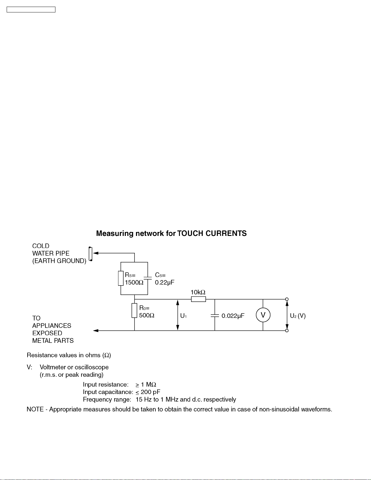
2.2. Touch-Current Check
1.Plug the AC cord directly into the AC outlet. Do not use an isolation transformer for this check.
2.Connect a measuring network for touch currents between each exposed metallic part on the set and a good earth ground such
as a water pipe, as shown in Figure 1.
3.Use Leakage Current Tester (Simpson 228 or equivalent) to measure the potential across the measuring network.
4.Check each exposed metallic part, and measure the voltage at each point.
5.Reserve the AC plug in the AC outlet and repeat each of the above measure.
6.The potential at any point (TOUGH CURRENT) expressed as voltage U
For a. c.: U
For d. c.: U
= 35 V (peak) and U2= 0.35 V (peak);
1
=1.0V,
1
Note:
The limit value of U
= 0.35 V (peak) for a. c. and U1= 1.0 V for d. c. correspond to the values 0.7 mA (peak) a. c. and 2.0
2
mA d. c.
The limit value U
= 35 V (peak) for a. c. correspond to the value 70 mA (peak) a. c. for frequencies greater than 100 kHz.
1
7.In case a measurement is out of the limits specified, there is a possibility of a shock hazard, and the equipment should be
repaired and rechecked before it is returned to the customer.
and U2, does not exceed the following values:
1
Figure 1
6
Page 7
TH-37PE30B / TH-42PE30B
3 Prevention of Electro Static Discharge (ESD) to
Electrostatically Sensitive (ES) Devices
Some semiconductor (solid state) devices can be damaged easily by static electricity. Such components commonly are called
Electrostatically Sensitive (ES) Devices. Examples of typical ES devices are integrated circuits and some field-effect transistors and
semiconductor "chip" components. The following techniques should be used to help reduce the incidence of component damage
caused by electro static discharge (ESD).
1.Immediately before handling any semiconductor component or semiconductor-equipped assembly, drain off any ESD on your
body by touching a known earth ground. Alternatively, obtain and wear a commercially available discharging ESD wrist strap,
which should be removed for potential shock reasons prior to applying power to the unit under test.
2.After removing an electrical assembly equipped with ES devices, place the assembly on a conductive surface such as alminum
foil, to prevent electrostatic charge buildup or exposure of the assembly.
3.Use only a grounded-tip soldering iron to solder or unsolder ES devices.
4.Use only an anti-static solder removal device. Some solder removal devices not classified as "anti-static (ESD protected)" can
generate electrical charge sufficient to damage ES devices.
5.Do not use freon-propelled chemicals. These can generate electrical charges sufficient to damage ES devices.
6.Do not remove a replacement ES device from its protective package until immediately before you are ready to install it. (Most
replacement ES devices are packaged with leads electrically shorted together by conductive foam, alminum foil or comparable
conductive material).
7.Immediately before removing the protective material from the leads of a replacement ES device, touch the protective material
to the chassis or circuit assembly into which the device will be installed.
Caution
Be sure no power is applied to the chassis or circuit, and observe all other safety precautions.
8.Minimize bodily motions when handling unpackaged replacement ES devices. (Otherwise hamless motion such as the brushing
together of your clothes fabric or the lifting of your foot from a carpeted floor can generate static electricity (ESD) sufficient to
damage an ES device).
7
Page 8
TH-37PE30B / TH-42PE30B
4 About lead free solder (PbF)
Note: Lead is listed as (Pb) in the periodic table of elements.
In the information below, Pb will refer to Lead solder, and PbF will refer to Lead Free Solder.
The Lead Free Solder used in our manufacturing process and discussed below is (Sn+Ag+Cu).
That is Tin (Sn), Silver (Ag) and Copper (Cu) although other types are available.
This model uses Pb Free solder in it’s manufacture due to environmental conservation issues. For service and repair work, we’d
suggest the use of Pb free solder as well, although Pb solder may be used.
PCBs manufactured using lead free solder will have the PbF within a leaf Symbol
Caution
·
· Pb free solder has a higher melting point than standard solder. Typically the melting point is 50 ~ 70 °F (30~40 °C) higher.
· ·
Please use a high temperature soldering iron and set it to 700 ± 20 °F (370 ± 10 °C).
·
· Pb free solder will tend to splash when heated too high (about 1100 °F or 600 °C).
· ·
If you must use Pb solder, please completely remove all of the Pb free solder on the pins or solder area before applying Pb
solder. If this is not practical, be sure to heat the Pb free solder until it melts, before applying Pb solder.
·
· After applying PbF solder to double layered boards, please check the component side for excess solder which may flow onto
· ·
the opposite side. (see figure below)
Suggested Pb free solder
There are several kinds of Pb free solder available for purchase. This product uses Sn+Ag+Cu (tin, silver, copper) solder.
However, Sn+Cu (tin, copper), Sn+Zn+Bi (tin, zinc, bismuth) solder can also be used.
stamped on the back of PCB.
8
Page 9
5 Service Hint
TH-37PE30B / TH-42PE30B
Stand the unit used for pedestal.
Remove the Rear Cover.
Service position.
Board Name Function
C1 DATA DRIVER (RIGHT)
C2 DATA DRIVER (LEFT)
D DIGTAL SIGNAL PROCESS
DG DIGTAL CORE, MICOM
G FRONT TERMINAL, SWITCH
H REAR TERMINAL
JG SD CARD/PC CARD, JPEG I/F D/A
K LED, REMOTE, POWER SWITCH
P POWER SUPPLY
PA DC/DC, AUDIO
PF LINE FILTER
S POWER SWITCH
SC SCAN DRIVE
SD SCAN OUT (DOWN)
SS SUSTAIN DRIVE
SS2 SUSTAIN CONNECTION (UP)
SS3 SUSTAIN CONNECTION (DOWN)
SU SCAN OUT (UP)
T TUNER
XV DVB TUNER
Remove the AV Connector Cover.
9
Page 10
TH-37PE30B / TH-42PE30B
6 P.C.Board and Plasma panel replacement method
n
n To replace the plasma panel (finished), place the unit on
nn
the servicing stand, remove the front frame (finished), and
replace the panel, being careful not to scratch the plasma
panel surface.
1.Remove the rear cover and the AV connector cover.
2.Remove the P-Board.
a.Remove the couplers (P2, P5, P7, P9, P11, P12, P23,
P25, P27).
b.Remove the screws (×5) and remove the P-Board.
5.Remove the XV-Board.
3.Remove the PA-Board.
a.Remove the couplers (PA1, PA2, PA3, PA4, PA5, PA6,
PA7, PA8, PA10A, PA12).
b.Remove the screws (×4
with the PA-Board Bracket.
c.Remove the screws (×6
4.Remove the D-Board.
a.Disconnect the couplers (D3, D4, D6, D12, D22, D25)
and the flexible cables (D31, D32).
b.Remove the screws (×7) and remove the D-Board with
the bracket.
) and remove the PA-Board
) and remove the PA-Board.
6.Remove the DG-Board, the H-Board and the T-Board.
a.Remove the couplers (DG2, DG3, DG6, DG8, DG10,
DG12, H9), a flexible cable (DG7), and the screws (×5
).
b.Remove the DG-Board, the H-Board and the T-Board
with the bracket.
c.Remove the bridge connectors (DG1-H1, DG4-H4) and
remove the screws (×3
d.Remove the DG-Board.
e.Remove the screws (×6
screws (×2
f.Remove the coupler (H10) and the antenna cable,
remove the T-Board with the T-Board bracket.
g.Remove the H-Board.
) on the T-Board bracket.
) on the DG-Board.
) on the H-Board and the
10
Page 11
h.Remove the screws (×2) and remove the T-Board.
7.Remove the PF-Board.
a.Remove the couplers (PF2, PF10).
b.Remove the screws (×5
), and remove the PF-Board
with the Bracket.
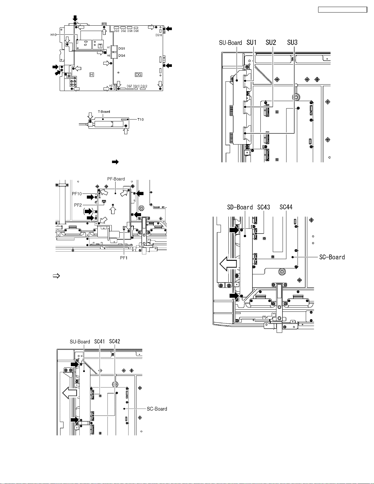
TH-37PE30B / TH-42PE30B
c.Remove the flexible cables (SU1, SU2, SU3) connected
to the SU-Board, and remove the SU-Board.
9.Remove the SD-Board.
a.Remove the screws (×2).
b.Slide the SD-Board to the left and disconnect from the
couplers (SC43, SC44) on the SC-Board.
c.Remove the coupler (PF1) and remove the screws (×5
).
d.Remove the PF-Board.
8.Remove the SU-Board.
a.Remove the screws (×2).
b.Slide the SU-Board to the left and disconnect from the
couplers (SC41, SC42) on the SC-Board.
11
Page 12
TH-37PE30B / TH-42PE30B
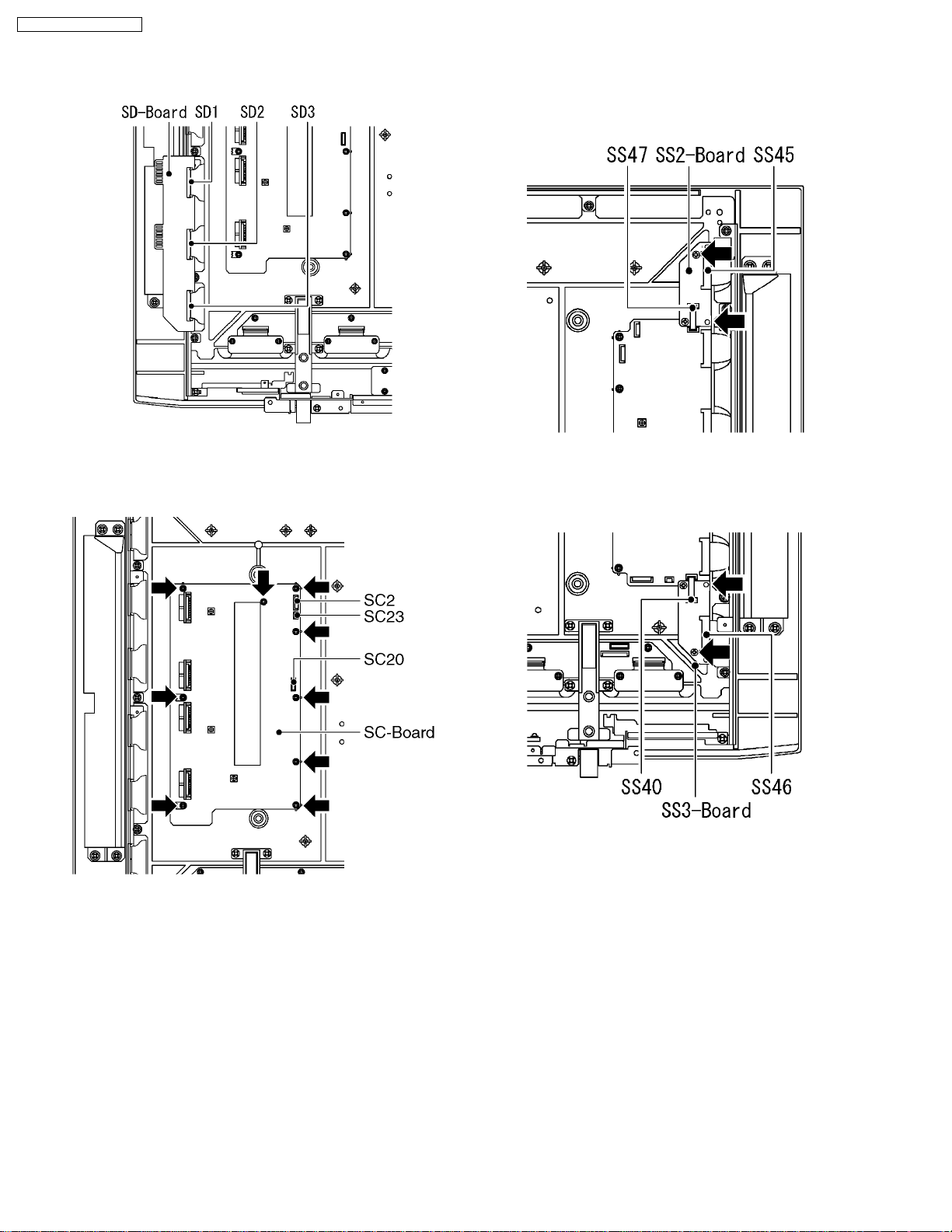
c.Remove the flexible cables (SD1, SD2, SD3) connected
to the SD-Board, and remove the SD-Board.
10.Remove the SC-Board.
a.Remove the couplers (SC2, SC20, SC23), the screws
(×9) and remove the SC-Board.
11.Remove the SS2-Board.
a.Remove the coupler (SS47), and remove the flexible
cable (SS45).
b.Remove the screws (×2), and remove the SS2-Board.
12.Remove the SS3-Board.
a.Remove the coupler (SS40) and the flexible cable
(SS46).
b.Remove the screws (×2), and remove the SS3-Board.
12
Page 13
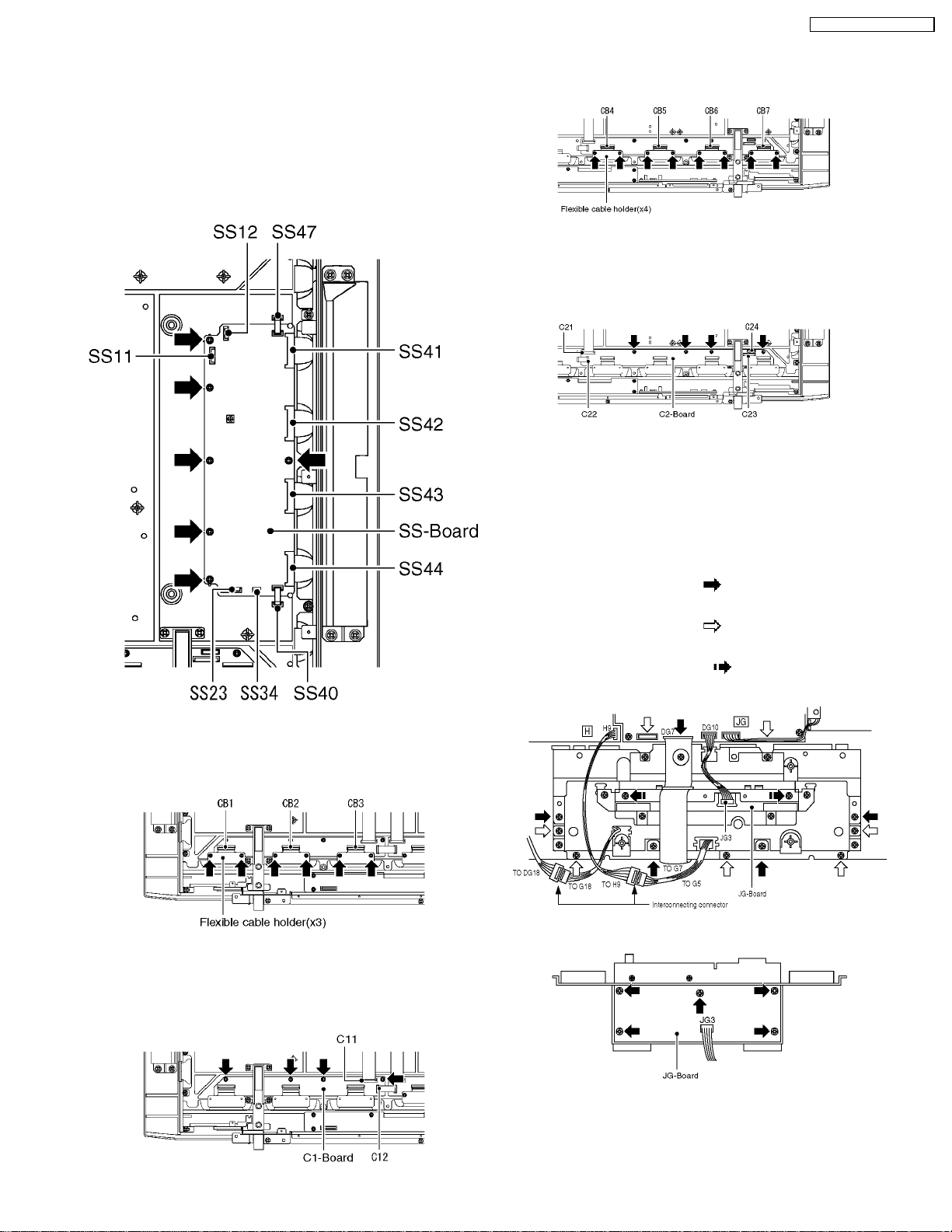
13.Remove the SS-Board.
a.Remove the couplers (SS11, SS12, SS23, SS34), and
remove the flexible cables (SS40, SS47) on the SS3Board and SS2-Board.
b.Remove the flexible cables (SS41, SS42, SS43, SS44).
c.Remove the screws (×6), and remove the SS-Board.
TH-37PE30B / TH-42PE30B
15.Remove the C2-Board.
a.Remove the flexible cable holder fastening screws (×8),
and remove the flexible cables (CB4, CB5, CB6, CB7).
b.Remove the couplers (C23, C24), a flexible cable (C21)
and release the speaker cables from the clamper on the
C2-Board.
c.Remove the screws (×4), and remove the C2-Board.
16.Remove the JG-Board and G-Board.
a.Remove the screws (×7) fixing the woofer speakers, the
interconnecting couplers (×4, to woofer and tweeter)
and remove the woofer speakers (right and left).
b.Disconnect a coupler (DG10), a flexible cable (DG7)
and the couplers of interconnecting connector (from
DG18 to G18 and H9 to G5).
c.Remove the screws (×5
) and remove the JG-Board
and G-Board with the Bracket.
d.Remove the screws (×7
) and remove the JG-Board
with Bracket.
e.Remove the screws (×2
) and remove the Shield
case of JG-Board.
14.Remove the C1-Board.
a.Remove the flexible cable holder fastening screws (×6)
and remove the flexible cables (CB1, CB2, CB3).
b.Remove the flexible cables (C11, C12) release the
speaker cables from the clampers (×2) on the C1Board.
c.Remove the screws (×4), and remove the C1-Board.
f.Remove the screws (×5) and remove the JG-Board.
13
Page 14
TH-37PE30B / TH-42PE30B
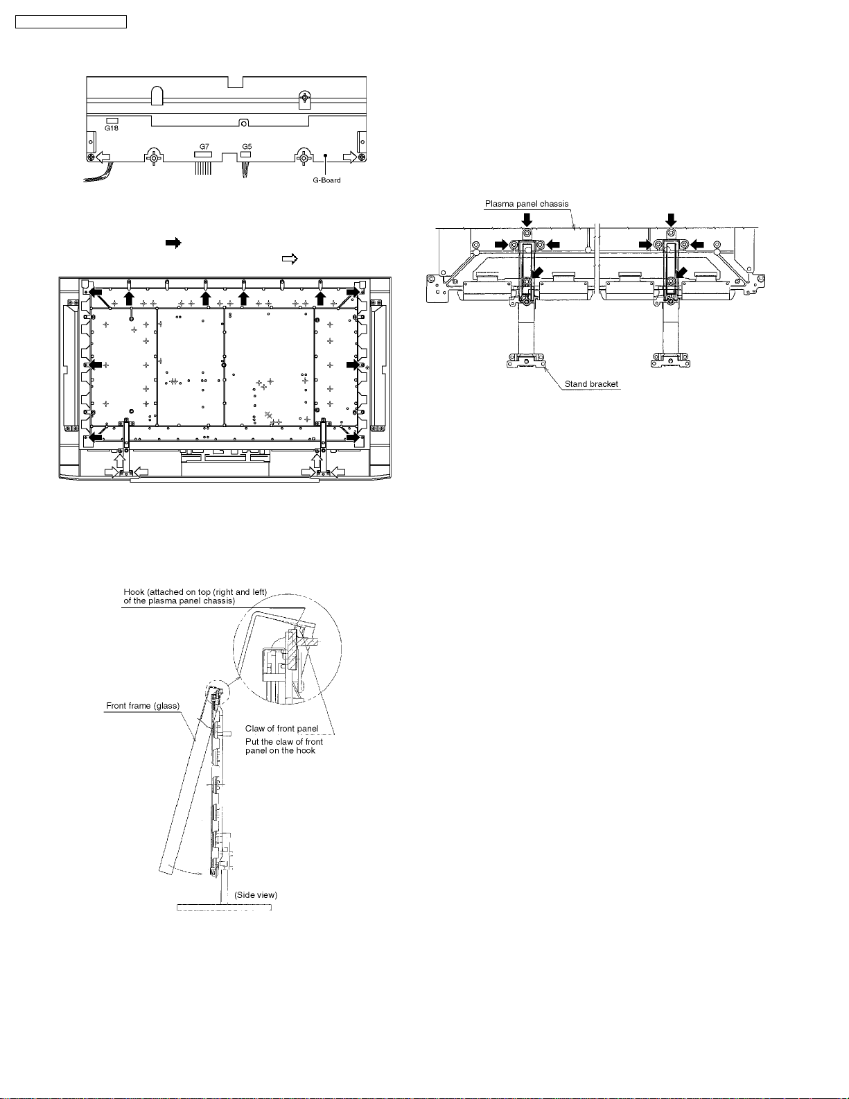
g.Remove the screws (×2) and remove the G-Board.
17.Remove the Front frame (glass).
a.Remove the front frame and the plasma panel fastening
screws (×10
stand braket fastening screws(×6
), and remove the front frame and the
).
b.Release all cables from the clamper on the bracket of
the front frame.
c.For leaving the the plasma panel from the front frame,
pull the bottom of the front frame forward, lift, and
remove.
18.Remove stand brackets.
a.Remove the plasma panel section from the servicing
stand and lay on a surface such as a table (covered),
with the plasma panel surface facing downward.
Spread a soft cloth or similar on the table for protection,
so the panel surface is not scratched.
b.Remove the stand bracket (left, right) fastening screws
(×4 each) and remove the stand brackets (left, right).
19.Replace the plasma panel (finished).
a.Place the new plasma panel (finished) on the flat
surface of the table (covered by a soft cloth), with the
plasma panel surface facing downward.
b.Fit the stand brackets (left, right) to the new plasma
panel.
c.Place the plasma panel section on the servicing stand.
d.Attach the front frame and the each P.C.Board and so
on, to the new plasma panel.
* When fitting the front frame, be careful not to allow
any debris, dust or handling residues to remain
between the front glass and plasma panel.
14
Page 15
7 Location of Lead Wiring
7.1. Lead of Wiring (1)
TH-37PE30B / TH-42PE30B
15
Page 16
TH-37PE30B / TH-42PE30B
7.2. Lead of wiring (2)
16
Page 17
7.3. Lead of wiring (3)
TH-37PE30B / TH-42PE30B
17
Page 18
TH-37PE30B / TH-42PE30B
7.4. Lead of wiring (4)
7.5. Lead of wiring (5)
18
Page 19
7.6. Lead of wiring (7)
TH-37PE30B / TH-42PE30B
19
Page 20
TH-37PE30B / TH-42PE30B
8SelfCheck
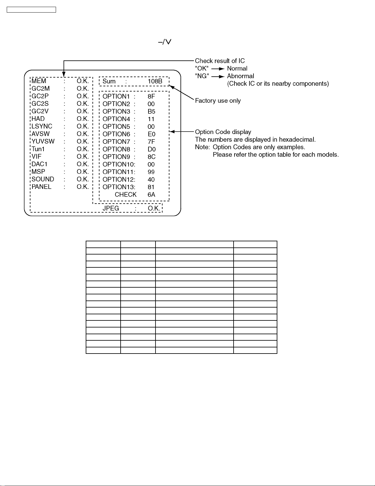
1.Self-Check is used to automatically check the bus lines and hexadecimal code of the TV set.
2.To get into the Self -Check mode press the Down (
time pressing the Status button on the remote control, and the screen will show :
) button on the customer controls at the front of the set, at the same
If the CCU ports have been ked and found to be incorrect or not located then “--” will appear in place of “O.K.”.
Display Ref.No Description P.C.B.
MEM IC1008 EEPROM DG-BOARD
GC2M IC1301 GROBAL CORE MAIN DG-BOARD
GC2P IC1304 GROBAL CORE SUB DG-BOARD
GC2S IC1302 GROBAL CORE 3D Comb DG-BOARD
GC2V IC1350 GROBAL CORE V Scalar DG-BOARD
HAD IC1851 HD-AD CONVERTER DG-BOARD
LSYNC IC2652 SYNC PROCESSOR H-BOARD
AVSW IC3200 AV switch H-BOARD
YUVSW IC1270 YUV switch DG-BOARD
Tun1 TNR001 TUNER 1 TU-BOARD
VIF --- --- --DAC1 IC3003 Ext. DAC DG-BOARD
MSP IC2002 Multi Sound Processor H-BOARD
SOUND IC2401 AUDIO AMP PA-BOARD
PANEL --- PANEL --JPEG IC60 JPEG I/F PG-BOARD
20
Page 21
TH-37PE30B / TH-42PE30B
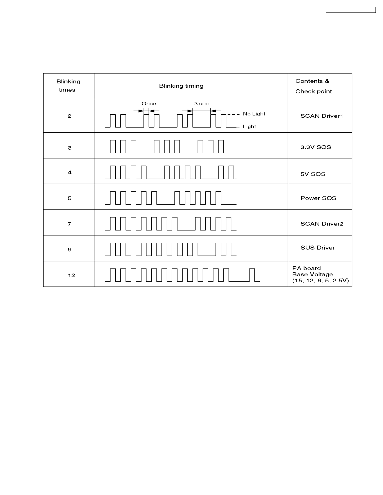
8.1. Power LED Blinking timing chart
1.Subject
Information of LED Flashing timing chart.
2.Contents
When an abnormality has occurred on the unit, the protection circuit operates and reset to the stand by mode. At this time, the
defective block can be identified by the number of blinkes of the Power LED on the front panel of the unit.
21
Page 22
TH-37PE30B / TH-42PE30B
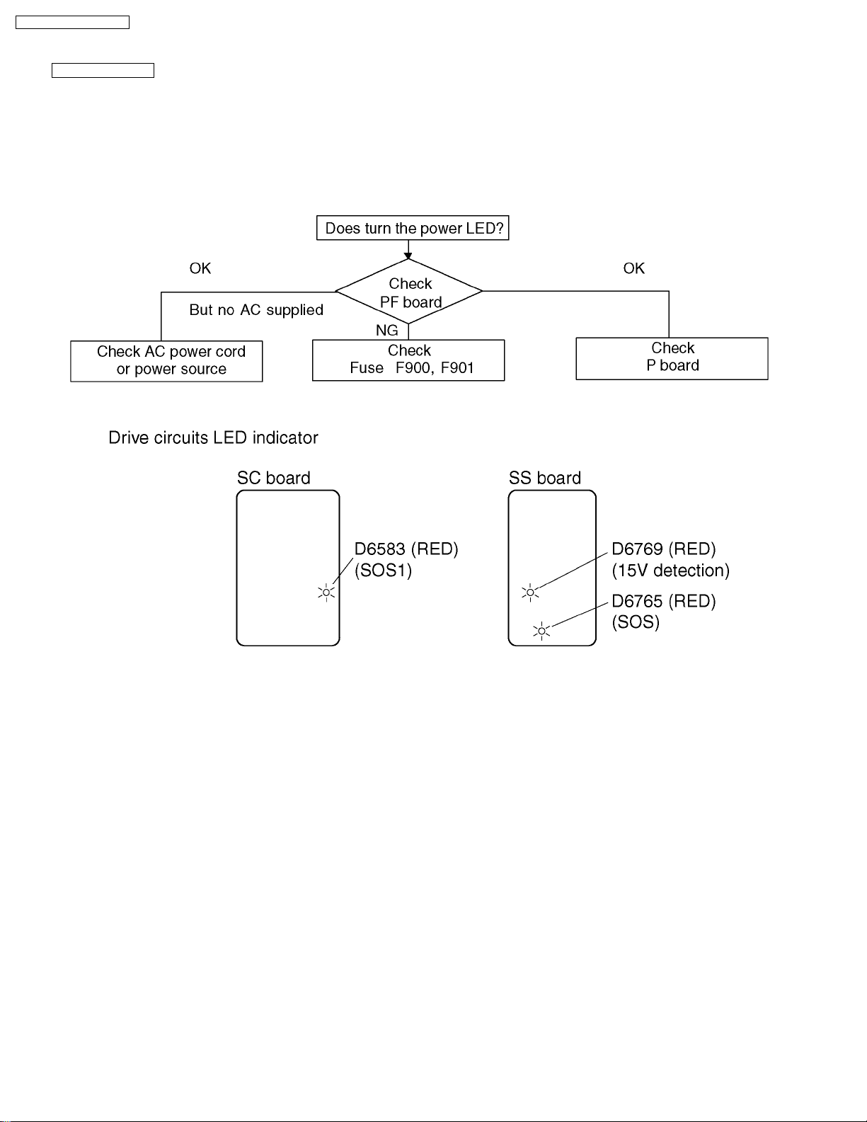
8.2. No Power
First check point
There are following 3 states of No Power indication by power LED.
1.No lit
2.Green is lit then turns red blinking a few seconds later.
3.Only red is lit.
1.No lit
22
Page 23
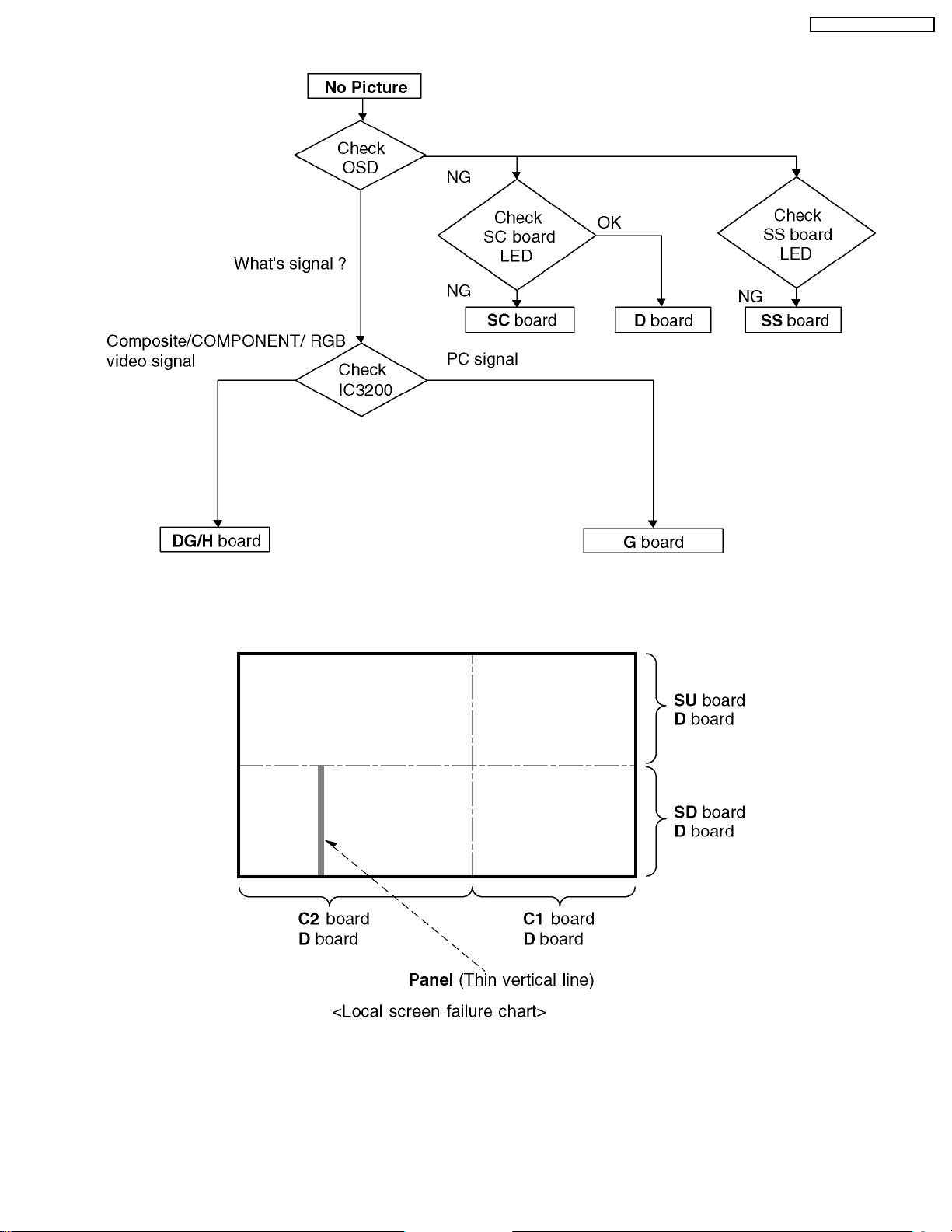
8.3. No Picture
TH-37PE30B / TH-42PE30B
8.4. Local screen failure
Plasma display may have local area failure on the screen. Fig - 1 is the possible defect P.C.Board for each local area.
Fig - 1
23
Page 24

TH-37PE30B / TH-42PE30B
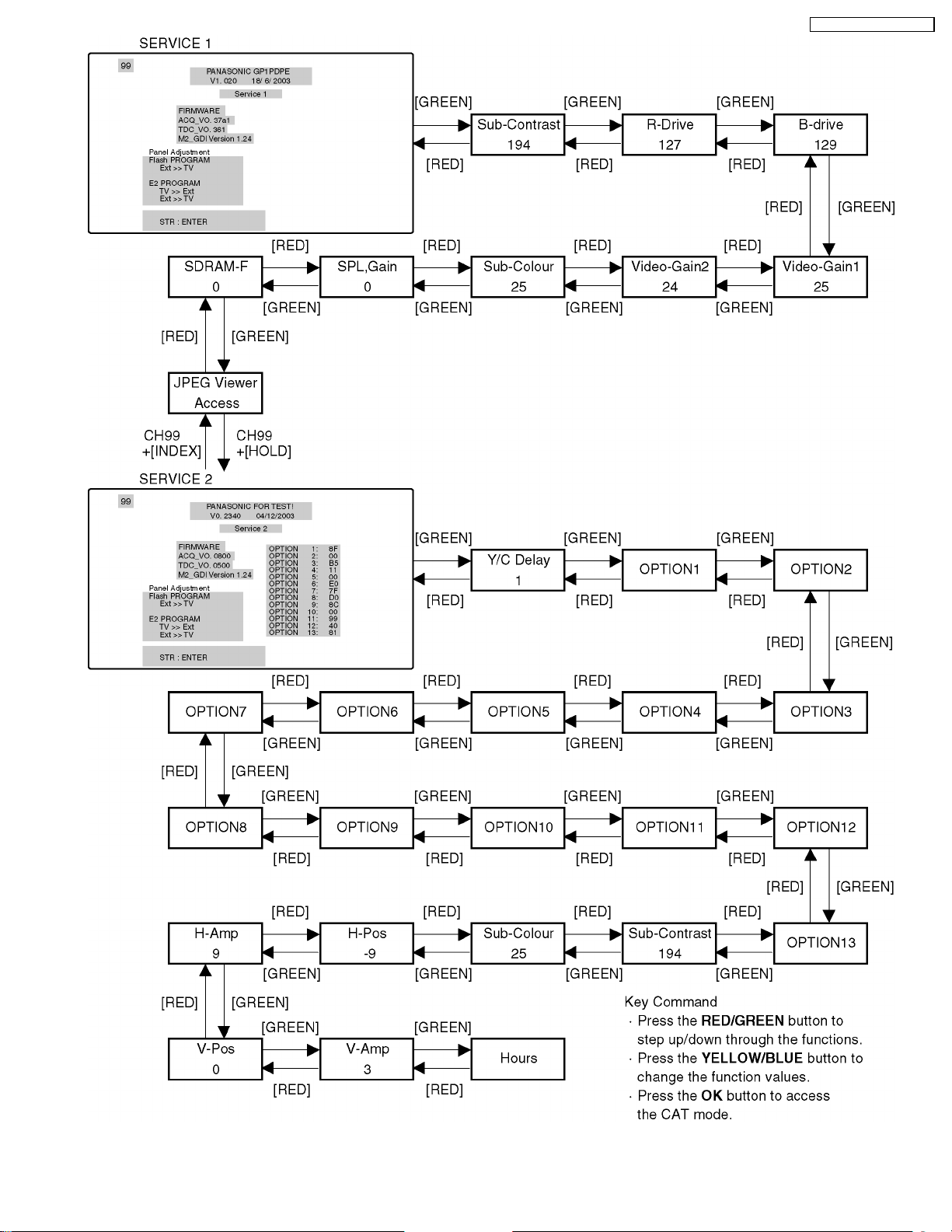
9 Service Mode Function
MPU controls the functions switching for each IICs through IIC bus in this chassis. The following setting and adjustment can be
adjusted by remote control in Service Mode.
9.1. How to enter SERVICE 1
1.In sound menu, set BASS to MAXIMUM, and set TREBLE to MINIMUM.
2.Simultaneously press INDEX button on remote control and DOWN button [
9.2. How to enter SERVICE 2
1.Set the channel to CH99.
2.Select the JPEG Viewer.
3.Press HOLD button on remote control.
Note:
To exit to Service mode, press N or Power button on remote control.
]ontheTVset.
24
Page 25
TH-37PE30B / TH-42PE30B
25
Page 26
TH-37PE30B / TH-42PE30B
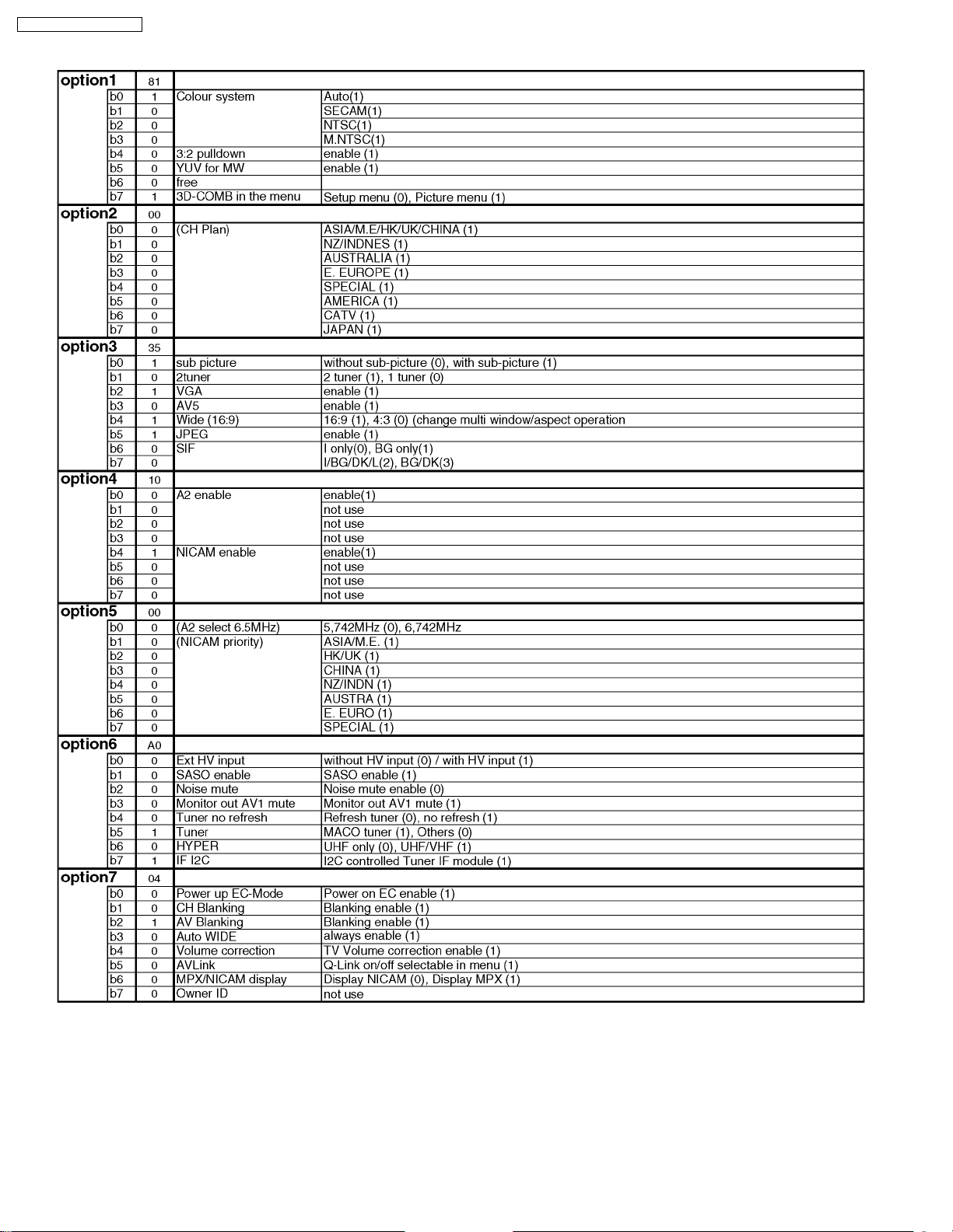
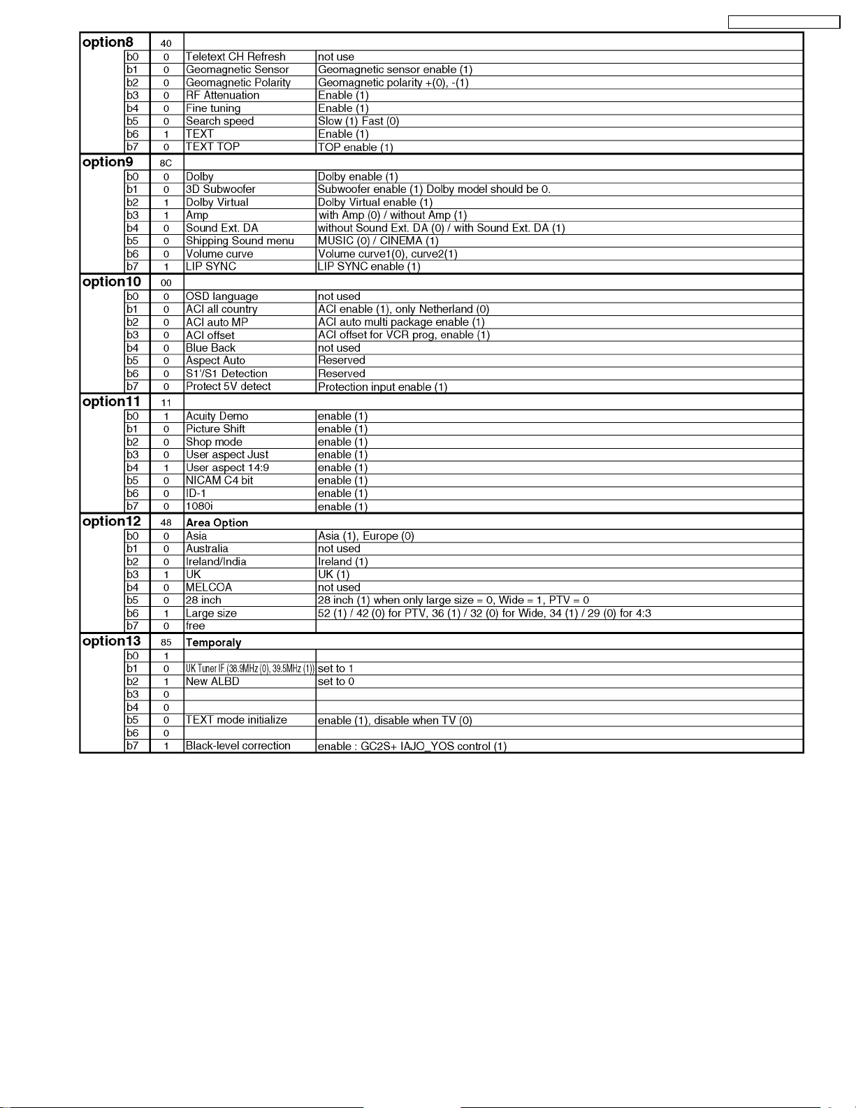
9.3. Option Description
26
Page 27
TH-37PE30B / TH-42PE30B
27
Page 28
TH-37PE30B / TH-42PE30B
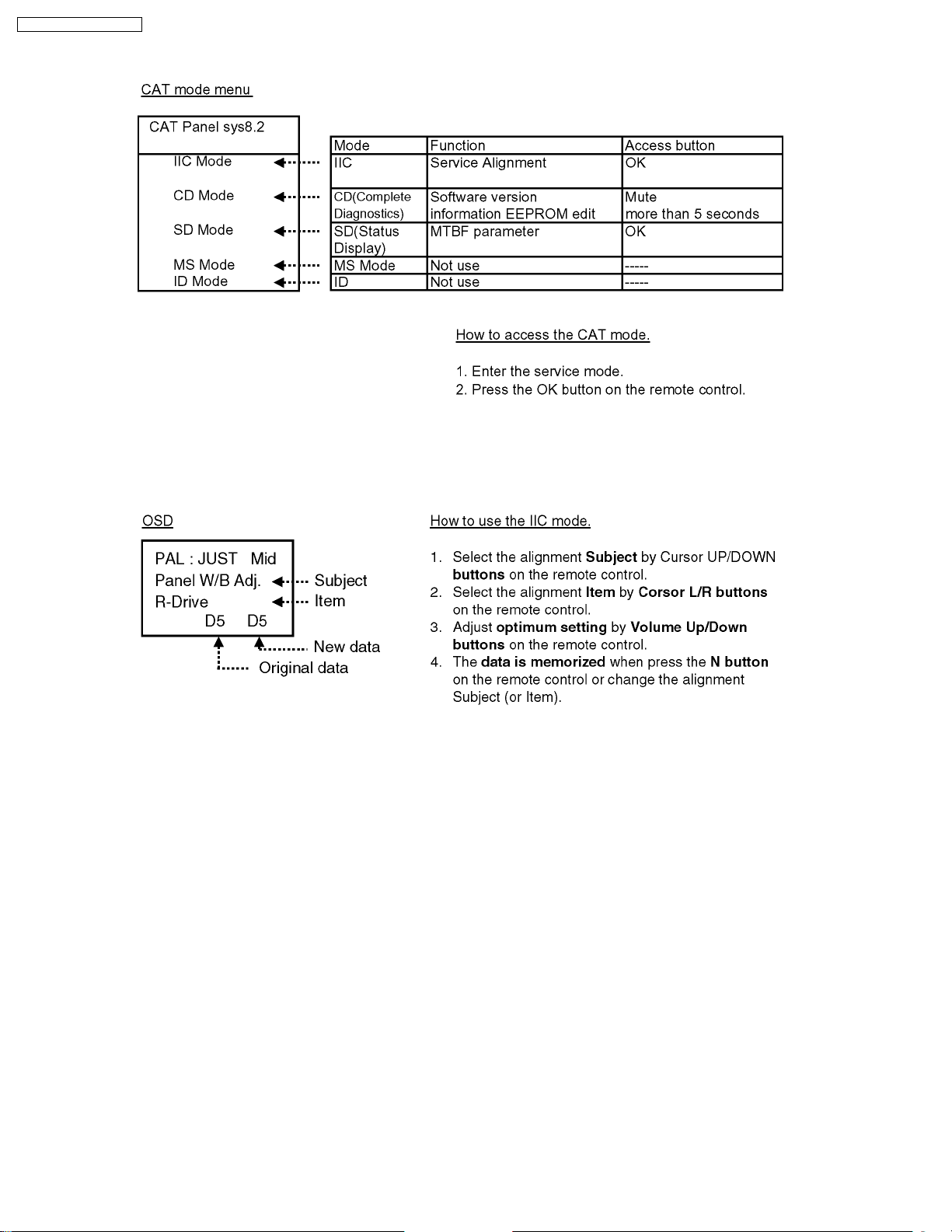
10 CAT (Computer Aided Test) mode
10.1. IIC mode
Select the IIC mode by Up/Down (Channel) button on the remote control at the front page of CAT mode then press the OK button
on the remote control.
Subject and item are mentioned on IIC mode structure.
(Refer to item 10.4.)
To exit the IIC mode, press the MENU button on the remote control.
28
Page 29
TH-37PE30B / TH-42PE30B
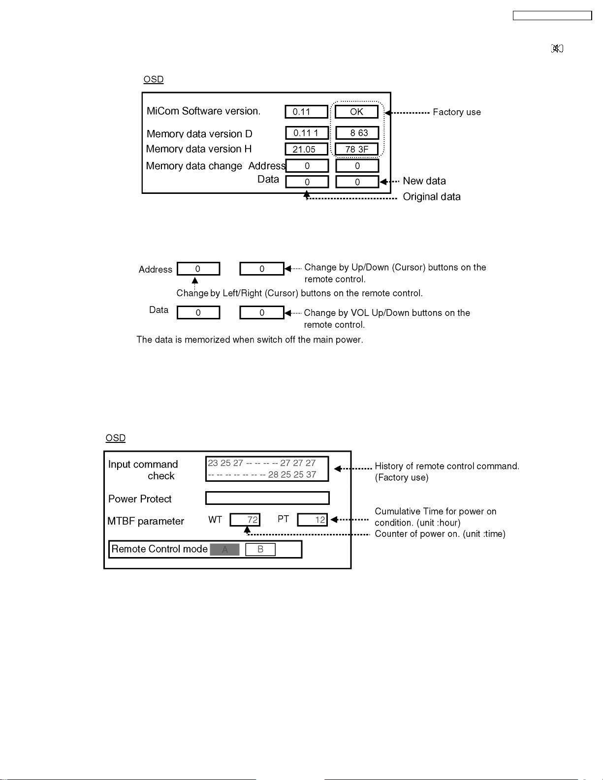
10.2. CD mode
Select the CD mode by Up/Down (Channel) button on the remote control at the front page of CAT mode then press the Mute
button on the remote control more than 5 sec.
Micom software version (IC1007), this version can be upgrade by replace of new version IC
Memory data change
To exit the CD mode, press the MENU button on the remote control.
10.3. SD mode
Select the SD mode by Up/Down (Channel) button on the remote control at the front page of CAT mode then press the OK
button on the remote control.
To exit the SD mode, press the MENU button on the remote control.
29
Page 30
TH-37PE30B / TH-42PE30B
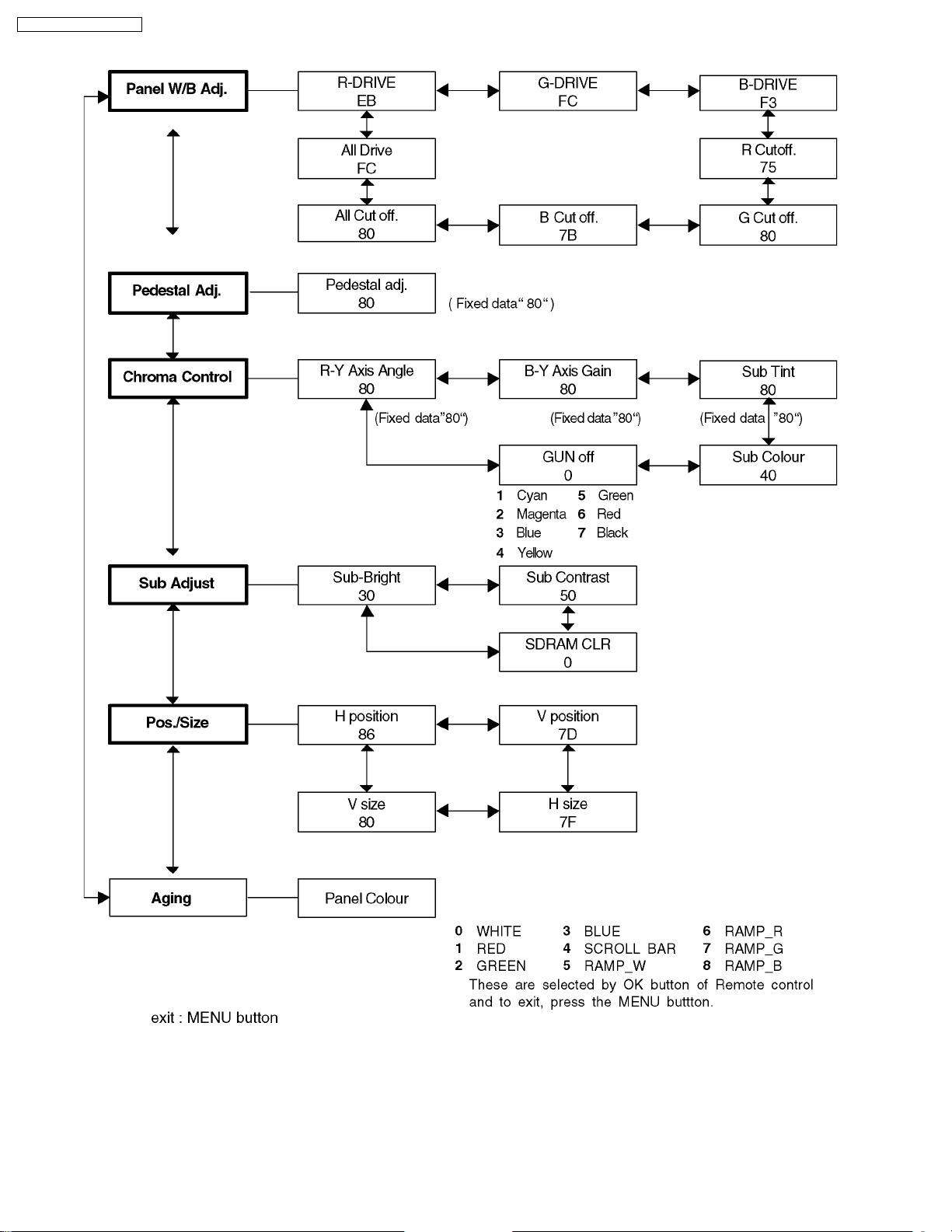
10.4. IIC mode structure (following items value is sample data.)
30
Page 31

11 Adjustment Procedure
TH-37PE30B / TH-42PE30B
11.2. Driver Set-up
11.1. +B Set-up
11.1.1. Item / Preparation
1.Input a Gray scale signal.
2.Set the picture controls: Picture mode: Normal
Colour balance: Normal
11.1.2. Adjustments
Adjust and confirm indicated test point for the specified voltage.
Adjust
Name Volume Voltage Test Point Remarks
Vsus R605 170V ± 1V P11 pin 2 P-Board
Vda R590 67V ± 0.5V P12 pin 1 P-Board
Confirm
Name Voltage Test Point Remarks
15V 15.4V ± 0.5V P23 pin 1 P23-3 (GND)
15V 15.2V ± 0.5V P7 pin 1 P7-3 (GND)
12V 11.8V ± 0.5V P25 pin 1 P25-3 (GND)
Audio+12V 12.5V ± 0.8V P5 pin 7 P5-9 (GND)
5V 5.1V ± 0.3V P25 pin 5 P25-6 (GND)
STB 5V 5.0V ± 0.3V P27 pin 4 P27-9 (GND)
PFC 380V ± 15V C468(+) C468 (-) (GND)
11.2.1. Item / Preparation
1.Input an APL 100 % white signal.
2.Set the picture controls: Picture mode: Normal
Colour balance: Cool
Aspect: 16:9
11.2.2. Adjustments
Adjust driver section voltages referring the panel data on the
panel data label.
Name Test Point Voltage Volume Remarks
Vsus TPVSUS
(SS)
Vbk TPVBK (SC) 155V ± 5V R6443 (SC)
Ve TPVE (SS) 158V ± 1V R6774 (SS)
Vset TPVSET
(SC)
Vad TPVAD (SC) -90V ± 1V R6477 (SC)
Vscn TPVSCN
(SC)
Vda TPVDA (SS) 67V ± 1V R590 (P)
*See the Panel label.
170V ± 1V R605 (P)
218V ± 6V ---
Vad*+118V ±2V---
31
Page 32

TH-37PE30B / TH-42PE30B
11.3. Initialization Pulse Adjust
1.Input a Cross hatch signal.
2.Set the picture controls: Picture mode: Normal
Colour balance: Cool
Adjust the indicated test point for the specified waveform falling period.
Test point Volume Level
T1 TPSC1 (SC) --- --T2 TPSC1 (SC) R6557 (SC) 170 ± 20µ Sec
32
Page 33

11.4. P.C.B. (Printed Circuit Board) exchange
11.4.1. Caution
1.To remove P.C.B. , wait 1 minute after power was off for discharge from electrolysis capacitors.
11.4.2. Quick adjustment after P.C.B. exchange
P.C.B. Name Test Point Voltage Volume Remarks
P Board Vsus TPVSUS (SS) 170V ± 1V R605 (P)
Vda TPVDA (SS) 67V ± 1V R590 (P)
SC Board Vbk TPVBK (SC) 155V ± 5V R6443 (SC)
Vad TPVAD (SC) -90V ± 1V R6477 (SC)
Vset TPVSET (SC) 218V ± 6V --Vscn TPVSCN (SC) Vad + 118 ± 2V ---
SS Board Ve TPVE (SS) 158V ± 1V R6774 (SS)
D, DG Board White balance, Pedestal and Sub brightness for NTSC, PAL, HD, PC and 625i signals
*See the Panel label.
11.5. Adjustment Volume Location
TH-37PE30B / TH-42PE30B
11.6. Test Point Location
33
Page 34

TH-37PE30B / TH-42PE30B
12 Alignment
12.1. Pedestal setting
34
Page 35

12.2. PAL panel white balance
TH-37PE30B / TH-42PE30B
35
Page 36

TH-37PE30B / TH-42PE30B
12.3. PC panel white balance
36
Page 37

12.4. Sub brightness setting
TH-37PE30B / TH-42PE30B
12.5. ABL Level
37
Page 38

TH-37PE30B / TH-42PE30B
13 Hotel mode
1.Purpose
Restrict a function for hotels.
2.Access command
·
· Enter to the Service 2 Mode.
· ·
·
· Press Status button on remote control and entry to the
· ·
EAROM EDITOR Mode.
·
· Set the data of EEPROM(ADDRESS 160) to C0.
· ·
Push the Power switch(button) off/on the set(the remote
control) to turn the set off/on.
It can be made Hotel mode.
3.Exit command
·
· First, set the data of EEPROM(ADDRESS 160) to 80.
· ·
Next, Push the Power switch(button) off/on the set(the
remote control) to turn the set off/on.
Then, it is no longer hotel mode.
4.Access command to the Hotel mode setup menu
·
· <Prerequisite> : It is conditions that the data of
· ·
EEPROM(ADDRESS 160) is C0.
In order to display the Hotel mode setup menu, please
enter the following command (within 2 second).
[TV]:down + [REMOTE]:TV/AV(3 times)
Then, the Hotel mode setup menu is displayed.
item Function
Initial INPUT Select input signal modes.
Initial VOL level Adjust output Volume.
Maximum VOl
level
Initial POS Select programme number.
Button lock Select local key conditions.
Remote lock Select remote control key conditions.
Set this signal, each time power is switched on.
<Selection> :
Off/TV/AV1/AV2/AV2S/AV3/Av3S/AV4/Av4S/AV4
C/PC
·
· Off: give priority to a last memory. However,
· ·
Euro model is compulsorily set to TV.
·
· AVnS/AVnC: only Euro model selectable
· ·
·
· PC: selectable with VGA option
· ·
Set this volume, each time power is switched on.
If the value of InitVol is changed, volume will
change. However, priority is given to a last
memory when InitVol is Off. When "InitVol" is
larger than "MaxVol", make "InitVol" and "MaxVol"
the same.
<Selection/Range> :
Off/0 to 100
·
· Off: give priority to a last memory
· ·
Adjust maximum volume.
Set this max. volume, each time power is
switched on.
When "MaxVol" is smaller than "InitVol", make
"MaxVol" and "InitVol" the same, if "InitVol" is not
Off.
<Range> :
0to100
Set this programme number, each time power is
switched on.
<Selection> :
Off/0 to 99 (Euro model)
·
· Off: give priority to a last memory
· ·
Set this condition, each time power is switched
on.
<Selection> :
Off/SETUPMENU/All
·
· Off: altogether valid
· ·
·
· SETUP: restrict F-key selection
· ·
(Tuning guide(menu) can not be selected.)
·
· MENU: restrict F-key selection
· ·
(only Volume/Mute can be selected.)
·
· All: altogether invalid.
· ·
Set this condition, each time power is switched
on.
<Selection> :
Off/SETUP/MENU
·
· Off: altogether valid
· ·
·
· SETUP: only Setup menu is invalid
· ·
·
· MENU: Picture/Sound/Setup menu are invalid
· ·
5.Explain the Hotel mode setup menu
CAUTION
This setup is not valid, unless data of
EEPROM(ADDRESS 160) will be C0, even if each
settings were done.
38
Page 39

14 Conductor Views
14.1. PF-Board
TH-37PE30B / TH-42PE30B
6
PF-BOARD (FOIL SIDE)
TXNPF1UHSE
PF
L970
R975
C975
JS25
L972
C974
D971
R983
C972
JS80
JS81
R974
R973
R976
IC970
J9
JS15
JS26
R984
D970
JS14
J14
C970
R982
4
R991
JS24
COLD
R981
TP979
C971
R987
R989
PF2
J2
JS23
S905
R980
C915
L973
R986
1
LF915C
JS13
JS72
C973
R985
LF915A
LF915B
S906
LF915
S912
S910
TP978
L971
R993
TP977
C911
C917
S911
JS70
C910
C903
S913
ZA901
C916
PF3
9
PF10
1
Parts Location
PF-BOARD (FOIL SIDE)
IC
IC920 B-5
IC921 C-5
IC970 D-5
TRANSISTOR
Q990 A-4
2
1
TP
TP901 B-4
TP902 B-5
TP903 B-5
TP904 A-5
TP977 D-5
TP978 D-5
TP979 D-5
JS71
R994
R922
TP903
5
C920
TP904
LIVE CIRCUIT
R932
HOT
R921
Q990
R992
COLD
JS73
T8AH 250V
CAUTION
+
C991
R920
D990
S903
C901
F900
1
4
R990
C990
3
S904
2
L921
TP902
R933
R938
RL901
J11
C925
R934
C927
R940
R930
J7
J6
-
R937
D920
R939
R931
TP901
TNPA2926
SEE REVERSE FOR ORDER NO.
CF901
R902
F901
R901
PF1
T8AH 250V
CAUTION
C930
C926
3
7
C929
LIVE CIRCUIT
LF904
LF904A
LF904B
LF904C
R927
LF911
S901
C923
R923
D921
P2
S3
PT
P1
C924
C922
IC920
4
5
D929
C928
D926
R929
R928
D927
D925
R936
R935
D928
L920
V2
1
6
C921
J8
D922
J5
R924
L922
V1
C931
T920
C914
IC921
S4 S2A
S1A S2B
S1B
R970
R971
J10
R972
JS16
HOT
J3
J4
2
PF
JS9
JS10
C908
CF902
R904
JS17
F902
JS18
T3.15AL 250V CAUTION
JS11
JS12
LF905
C902
J1
C909
LF909C
S909
LF909
LF909A
LF909B
1
TH-37/42PE30B
PF-BOARD TXNPF1UHSE
A
4
JS27
S915
COLD
TH-37/42PE30B
PF-BOARD TXNPF1UHSE
C E GIBDFH
39
Page 40

TH-37PE30B / TH-42PE30B
6
PF-BOARD (COMPONENT SIDE)
TXNPF1UHSE
PF
D971
C973
JS72
C972
L972
L970
S3
S4
JS80
S1A S2B
S1B
S2A
J10
J9
LF915
LF915B
5
JS16
6
LF915C
JS17
D970
PF2
JS13
LF915A
J14
C970
C971
COLD
4
10
8
JS14
4
7
1
JS15
329
9
PF10
5
1
JS70
C910
C903
4
C911
C917
3
L973
L971
1
1
3
2
J2
C915
T920
AK
IC921
C914
R904
P2
D921
P1PT
L920
V2
V1
L922
PbF
R923
R924
J5
J3
IC920
C921
LF911
TNPA2926
C924
1
6
J8
94V-0
J4
D929
ORDER
NO.
2
R922
C923
L921
3
4
5
D927
PF
C920
R933
J11
7
J6
C929
J7
-
HOT
JS71
R939
R932
R931
R921
R920
D920
LIVE CIRCUIT
LIVE CIRCUIT
HOT
+
RL901
C990
COLD
JS73
Parts Location
PF-BOARD (COMPONENT SIDE)
IC
IC920 C-5
IC921 C-5
C916
2
1
PF3
2
ZA901
1
TH-37/42PE30B
PF-BOARD TXNPF1UHSE
A
JS24
F902
8
JS25
3
6
LF909A
LF909
1
12
4
15
JS23
7
11
JS18
T3.15AL 250V
JS26
5
9
2
13
14
LF909C
CAUTION
LIVE CIRCUIT
HOT
LF909B
C902
J1
JS12
11
14
C909
COLD
JS11
LF905
LF904C
15
JS9
CF902
LF904
LF904A
5
1
4
12
10
18
13
JS10
C908
8
LF904B
S901
6
16
9
17
7
T8AH 250V
CAUTION
JS27
S915
F901
R902
1
3
2
3
2
C901
CF901
T8AH 250V
CAUTION
R901
F900
1
PF1
4
TH-37/42PE30B
PF-BOARD TXNPF1UHSE
C E GIBDFH
40
Page 41

14.2. P-Board
P-BOARD (FOIL SIDE)
6
5
4
3
2
1
TNPA3336
P11
1
R600
R597
C566
D553
R557
C550
TH-37PE30B / TH-42PE30B
P
IC554
Q552
D
A
K
R
C562
HOT
C467
P12
5
1
R610
KRA
G
S
IC557
C567
R582
R586
D566
C578
R611
R609
D580
D578
R612
EBC
R593
Q553
R596
R599
R594
R595
R608
D579
Q554
B
C
E
R607
R601
D575
D576
C565
D574
D577
C571
D660
D661
S8S7S9S5S6S3S4S2S1
T502
P2
P1
PT
V4
V2
V3
V1
C591
C577
14
R621
P7
C590
13
1
3
1
T401
P1PT
P25
5
P10
D587
2
R620
S1 S2
8
11 1
L554
D589
C579
R618
C414
V1
V2
V3
L401
R411
D407
P23
C422
C421
R619
C572
C564
R562
D568
D582
L552
C576
D573
D581
C570
1
COLD
C581
IC555
R559
5
4
C583
R615
P2
D
D406
R404
R402
C
IC401
C406
C405
C455
LIVE CIRCUIT
G
D455
R464
D
D
D457
R463
S
Q451
C466
L452
Q454
G
R468
D456
R467
S
D462
P30
PFC
R462
R563
R578
R572
C559
R475
R471
R504
D454
C459
R480
R474
R473
R479
R478
R472
HOT
R652
D652
TNPA3336
SEE REVERSE FOR ORDER NO.
R477
R476
R469
B
B
Q452
Q453
C456
R465
R456
D453
9
R466
R470
R494
8
C
C
L451
IC451
E
D463
C464
E
D452
C650
C465
C548
D550
IC550
2
3
1
HOT
R409
C408
C452
C451
C454
C549
C462
C457
R461
C472
C463
R481
1
P
C461
16
R453
C460
R460
C458
1
R482
+
R459
-
D451
R452
C453
R458
R457
R451
R455
R454
D409
C404
1
Q558
R418
V4
C401
C587
9
P27
C586
P5
R630
R628
R631
R419
C417
C416
IC402
R415
R416
KRA
C415
C412
C411
C410
S
D405
C407
R627
Q406
C423
C585
C584
R420
EBC
R422
C
D411
B
Q404
R421
R417
D410
R414
R571
C409
C420
C418
C413
R428
R426
R413
R412
D408
Q405
R436
D413
R435
BC
E
R434
R407
R410
R408
R433
C403
TP50
TP51
D412
E
C419
IC403
312
R427
Q403
EBC
R424
Q402
E
C
R423
B
Q401
EBC
R425
R432
PbF
R431
R430
R429
Parts Location
P-BOARD (FOIL SIDE)
Q452 E-2
Q453 E-2
Q454 D-2
Q455 B-2
Q456 B-2
Q457 B-2
Q552 C-5
Q553 D-5
Q554 D-6
Q555 B-6
Q557 C-6
Q558 F-5
Q650 B-2
Q651 B-2
TP
TP008 G-1
TP009 G-1
TP50 G-5
TP51 G-5
TPP1 C-4
RL401
C402
D404
RL403
RL402
TP008
R406
1
IC
IC401 F-4
IC402 F-5
IC403 G-5
IC451 E-2
IC550 E-2
IC551 A-2
IC552 C-2
D401
D403
D402
P9
3
TP009
IC553 C-4
IC554 C-5
IC555 F-5
IC557 C-5
IC558 B-6
TRANSISTOR
Q401 G-4
Q402 G-5
Q403 G-5
Q404 G-5
Q405 G-4
Q406 G-4
Q451 D-3
IC558
S1
R555
R598
R552
COLD
D572
STA STB
R613
D584
R616
R554
D585
C569
T501
D570
D567
7
P2
16
C573
PTAP1
D560
C558
C551
1
2
3
4
5
IC551
R565
D557
R483
C469
R550
R560
R484
C557
R568
C470
R577
R570
R574
C554
R654
R567
Q457
C
B
Q456
D555
B
R489
R487
R488
Q455
D551
R502
R503
R485
R486
R587
R575
C
C575
R493
R490
D458
R614
D561
R491
EBC
D459
D590
Q555
R617
D583
C574
R592
S2 S4 S3
P2PTB
R579
R650
D562
D650
D651
R657
C
E
B
C
B
R656
E
E
R492
C471
D460
D552
C468
Q557
R623
R625
D571
V2
COLD
R602
R604
R603
R606
R584
C561
D564
R573
C553
R605
D596
D594
Vsus
R589
R635
R561
C568
R591
R
R581
R566
C552
R590
A
K
L551
R585
D565
C555
D556
2
4
IC552
R564
R588
Vda
R583
C563
TPP1
R580
D559
R558
D554
94V-0
D563
1
3
R551
C560
R576
R569
R553
5
D595
R626
D592
D593
D586
IC553
V1
C556
D654
R655
Q651
Q650
E
R653
R556
D558
TH-37/42PE30B
P-BOARD TNPA3336
A
TH-37/42PE30B
P-BOARD TNPA3336
C E GIBDFH
41
Page 42

TH-37PE30B / TH-42PE30B
P-BOARD (COMPONENT SIDE)
6
5
TNPA3336
Q403
Q402
Q401
C419
3
PMM3
Q404
2
1
C420
IC403
P27
R594
COLD
1
IC554
Q552
Vda
R590
PMM2
L551
IC553
ARK
G
D
S
IC557
ARK
D566
134
S1
P25
1
P10
1
C581
IC555
52
COLD
C576
PMM4
C572
C570
P23
D573
C421
L552
3
C564
C422
1
C577
C590
D568
P7
COLD
D574
C591
D660
T502
Q554
C571
S7S8
S6S5S9
1
4
9
11
P5
C585
R628
Q558
C417
C418
IC402
R
A
K
R412
C413
T401
C416
8
1
1
5
L554
C579
C414
S2
C565
P12
5
C578
ARK
C
Q553
E
B
R595
S3
S1
S2
S4
R605
Vsus
T501
Q557
R592
Q555
R587
IC558
C575
K
C574
R554
R
A
6
R552
1
P11
1
R600
R597
7
R598
P2
PMM1
C573
C566
C569
S1STASTBS2S4S3
D570
P
D408
4
3
2
PbF
R406
C403
C402
Q406
C409
RL403
RL402
C412
D404
C410
RL401
V4
S
V3 V2
IC401
C406
C404
HOT
C455
R411
L401
P2
P1 PT
V1
DIP
D
C
C405
C408
R409
C452
C451
D406
HOT
1
IC550
3
2
LIVE CIRCUIT
C549
C650
C462
C457
16
C465
IC451
+
D451
C454
1
C464
-
R404
C453
R451
R455
R452
R458
R652
C548
C456
9
Q452
Q453
V2
V1 V3
V4
P2PTP1
TNPA3336
ORDER
L451
R463
R467
C466
R464
R468
NO.
Q451
G
D
S
Q454
G
D
S
R563
R578
R572
P30
C559
R456
PFC
R469
8
C459
L452
R475
R462
TPP1
94V-0
1
P
HOT
D563
R569
R576
C563
D565
R580
C555
D567
Parts Location
V2 V1 P2 PTB PTA P1
D560
C556
IC552
1
2
D558
Q650
D552
3
4
5
C560
C468
R650
C471
R655
Q651
Q455
R579
R570
R485
R577
C470
Q457
Q456
D551
C557
R574
R568
R560
IC551
R550
R483
C558
3
D557
1
2
4
5
C469
IC
IC401 B-4
IC402 A-5
IC403 A-5
IC451 C-3
IC550 C-4
IC551 F-2
IC552 E-3
IC553 E-5
IC554 D-6
IC555 B-5
IC557 E-5
IC558 F-6
P-BOARD (COMPONENT SIDE)
TRANSISTOR
Q401 A-4
Q402 A-5
Q403 A-5
Q404 A-5
Q406 A-4
Q451 D-3
Q452 C-2
Q453 C-2
Q454 D-2
Q455 F-2
Q456 F-2
Q457 F-2
Q552 D-5
Q553 D-5
Q554 D-6
Q555 F-6
Q557 E-6
Q558 A-5
Q650 F-2
Q651 F-2
TPP1 E-4
1
TH-37/42PE30B
P-BOARD TNPA3336
3
1
P9
C401
R402
R454
R457
D462
D457
C467
R553
R551
TH-37/42PE30B
P-BOARD TNPA3336
A
C E GIBDFH
42
Page 43

14.3. PA-Board
TH-37PE30B / TH-42PE30B
6
5
4
3
2
1
PA-BOARD (FOIL SIDE)
TXNPA1UHSE
C2353
C2382
JK7001
SEE REVERSE FOR ORDER NO.
TNPA2989
2
TPB7501
JK7002
PA
TPB7516
TPB7509
C2403
D7517
TPB7506
R7585
C7586
R2401
R2402
R7547
TPB7504
R2408
C2402
R2404
C2401
R2403
C2416
C7585
TPB7520
R7546
R7545
R2381
R2382
C2404
C2418
TPB7502
R7583
R7591
R2359
R2405
C2420
TPB7505
L7581
Q7581
C2351
R2406
C2408
C2422
C7581
C2424
R2407
C2426
D7581
R2409
C2429
TPB7510
C2412
R2352
R2360
D7538
D7537
R7522
R7521
TPB7503
C7521
C7534
R2361
C2417
L7513
C2419
L7515
C2350
C2356
C2357
C2421
R2351
R2430
C2423
C2432
D7514
C2425
C2431
R7514
R2364
C2427
1
2
C7523
L2350
C2354
R2353
3
L7514
C7522
C7525
TPB7508
R2350
C2415
IC7505
C2428
C7524
R2314
C2328
5
R7516
4
R7531
R7511
PA
1
PA9
R2339
B
R2311
C2321
E
L2301
C2317
C2307
C7570
R7505
D7505
C2315
28
R2301
1
C2305
C2301
C2331
4
1
2
5
3
D7506
L7505
C7506
R7504
C7569
C7509
C7561
R7580
1
D7553
PA23
R7590
8
R7595
C2338
C2303
R2303
IC7502
C7536
R7503
7
1
R2318
PA24
C2398
R2326
R2309
R2444
L7501
C7501
C7530
L7503
C7552
1
PA22
12
PA4
1
C2443
14
C7571
C2400
R2328
1
L2310
C2390
15
C2355
C2430
1
2
3
D7503
C7503
C7502
L7552
7
1
4
1
12
1
R2336
C2386
5
L7502
R7502
PA21
PA25
IC2306
IC7501
4
C7553
PA3
C7504
R7560
R7551
PA12
R7501
R7558
C7554
TPB7514
R2338
TPB7518
C7535
R7555
C2348
R7557
4
TPB7513
C2388
7
L2308
D7566
R2324
D2305
R2340
R2337
IC2305
C2347
C2345
R2329
R2323
C2391
L2307
C2112
C2387
28
1
R2321
C2413
L2309
C2392
C2397
R2325
28
1
R2322
R2330
C2346
C2349
R2335
C2399
C2389
R2327
C2393C2394
1415
C2385
C2381
JK7005
PA7
1
4
11 1
PA5
Parts Location
PA-BOARD (FOIL SIDE)
TP
TPB7501 A-3
TPB7502 A-2
TPB7502 A-3
TPB7504 A-3
TPB7505 A-3
TPB7506 A-3
TPB7507 F-3
TPB7508 B-2
TPB7509 A-4
TPB7510 A-2
TPB7512 E-3
TPB7513 E-3
TPB7514 E-1
TPB7515 D-2
TPB7516 A-4
TPB7517 E-3
TPB7518 E-3
TPB7519 F-3
TPB7520 A-2
TPB7521 F-3
TPB7522 F-3
TPB7523 F-3
R7552
C7563
L7563
C7562
L7562
L7551
C7551
1
PA17
C7574
TPB7517
TPB7512
10
TPB7523
1
1
D7564
1
D7563
1
1
R7564
PA14
R7563
PA13
R7562
PA11
TPB7521
PA10
PA10A
JK7007
9
1
1
C7568
R7561
D7576
D7562
R7576
R7579
PA16
3
PA15
3
3
3
3
TPB7522
TPB7519
C7565
R7569
R7568
L7561
4
TPB7507
JK7004
R7587
C7564
R7565
R7596
C7567
D7561
IC
IC2301 D-4
IC2302 B-4
IC2305 F-4
IC2306 E-4
IC7501 E-3
IC7502 D-3
IC7504 C-3
IC7505 B-3
TRANSISTOR
Q2301 D-5
Q2302 B-5
Q2305 C-4
Q7509 C-2
Q7510 C-2
Q7581 A-2
R2315
C7510
IC7503
6
Q2301
C
R2333
R2331
C2325
C2333
IC2301
C2313
L7504
C7505
C7531
L7506
R7506
TPB7515
JK7003
1
Q2302
C
L2304
R2334
R2332
C2330
C2334
R2316
C2326
15
IC2302
14
C2310
C2314
R7523
L7512
D7508
C7516
R7524
1
2
3
D7532
C7518
D7511
L7510
C7526
C7533
R7512
D7513
B
E
L7511
C2318
C7517
D7502
C2308
C7573
L2302
R7509
C2332
5
PA1
R2312
C2316
28
R2302
1
4
IC7504
5
R7518
R7510
C7519
Q7509
C7515
C2306
R2310
C2322
C2337
R7520
L7507
C7511
C2302
R2392
R7519
C2304
R2304
C7532
L7509
R2391
C2342
C2339
R2396
C2352
JK7006
C7513
R2395
C7572
Q7510
R7589
R7588
L2303
C2327
C2329
R2375
R2313
R2376
Q2305
15
R2393
14
R2394
C2309
C2344
4
1
2
5
3
D7509
C7537
L7508
R7507
R7508
C7514
C7512
R7517
R7515
TH-37/42PE30B
P A-BO ARD TXNPA1UHSE
A
TH-37/42PE30B
P A-BO ARD TXNPA1UHSE
C E GIBDFH
43
Page 44

TH-37PE30B / TH-42PE30B
6
5
4
3
2
1
PA-BOARD (COMPONENT SIDE)
TXNPA1UHSE
D2305
C7568
C2387
Q2313
C
L2309
B
E
C2389
R2327
C2393
C2395
C2383
C2347
C2385
C2349
JS7521
JS2101
JS2102
JS2103
JS2104
JS2105
PA
2
R7575
Q7567
Q7564
Q7563
R7567
C7564
R7577
Q7561
Q7562
L7561
R7566
C7538
5
IC7561
D7565
NP
C7565
D7567
IC7562
JK7004
R2324
C2392
C2397
C2399
L2308
R2325
C2388
15
14
R2319
R2317
Q7565
R7573
R7582
R7581
C7566
5
1
R7578
C7562
L7551
1
C7551
L7562
PA17
4
JS2107
JS7528
JS7525
JS2106
14
1
11
JK7005
L2306
PA5
IC2304
IC2102
PA7
C2113
JK7007
C2414
10
9
1
1
D2317
D2316
JS2301
TNPA2989
ORDER
PA10
PA10A
NO.
PA16
PA15
PA14
PA13
PA11
C2413
C2391
1
R2323
D2303
L2307
C2112
28
IC2305
1
JS2303
C2345
C2381
ABACADAEAF
3
1
3
3
1
1
3
D7568
3
1
IC2306
R7572
PA
JS2302
Q2308
C2353
C7533
D7513
C2328
R2314
R2358
R2363
D2352
Q2352
L2350
D2350
R2355
R2354
C2350
Q2350
Q2355
R2367
NP
C2415
R2356
R2421
R2416
C2428
15
R2420
IC2401
17
R2419
R2423
R2431
C7522
R2422
C2433
4
IC2402
5
8
C2436
R2434
C2437
IC7505
1
4
L7514
3
C7525
14
R2417
R2435
Q7507
R2357
D2314
Q2351
R2378
D2351
JS2304
C2356
Q2303
Q2353
Q2356
Q2354
R2362
R2366
C2357
Q2315
R2383
C2407
R2413
R2412
16
R2415
R2418
C2410
R2414
R7526
1
D7539
D7540
R7537
R7538
Q7544
L7513
R7594
R7533
D7541
2
D7542
C7521
D7512
L7581
R7586
C7534
C7582
L7515
R7528
R7530
Q7506
32
R7539
R2377
R2385
D2315
D2311
JK7001
R2371
Q2304
2
PA2
Q7504
20
C2403
40
C7585
R2374
R2373
R2372
C2382
D2312
19
R2384
C2358
2
1
PA6
PbF
R7544
C7544
C7542
R7543
R7548
39
Parts Location
PA-BOARD (COMPONENT SIDE)
Q7501 D-2
Q7502 D-2
Q7503 E-2
Q7504 G-3
Q7505 D-2
Q7506 F-2
Q7507 F-2
Q7511 E-2
Q7532 B-2
Q7541 F-3
Q7542 F-4
Q7543 F-3
Q7544 F-3
Q7551 C-1
Q7552 C-2
Q7553 C-2
Q7561 B-2
Q7562 B-2
Q7563 B-3
Q7564 B-3
Q7567 B-3
Q7582 G-2
Q7582
JK7002
D7518
D7582
C7583
C7584
R7584
D7516
IC
1
IC2102 A-5
IC2301 C-4
IC2302 E-4
IC2304 A-4
IC2305 A-4
IC2306 B-4
IC2401 F-4
IC2402 F-4
IC2403 C-3
IC7501 C-3
IC7502 D-3
IC7503 D-3
IC7504 E-3
IC7505 F-3
IC7551 C-2
IC7561 B-2
IC7562 B-2
IC7581 F-2
TP
Q2301 D-5
Q2302 E-5
Q2303 F-5
Q2304 G-5
Q2306 E-4
Q2307 F-5
Q2308 F-5
Q2309 D-4
Q2310 E-3
Q2311 E-3
Q2312 D-3
Q2313 B-5
Q2314 C-5
Q2315 F-5
Q2350 F-5
Q2351 F-5
Q2352 F-5
Q2353 F-5
Q2354 F-5
Q2355 F-5
Q2356 F-5
R2494
C2351
Q2307
R2380
R2379
D2310
C2404
NP
NP
R2428
1
R2427
D2401
D2402
C2408
Q7542
D7546
R7527
C7543
R7549
R7550
R7559
R7536
R7535
R7542
R7534
R7541
Q7541
R7532
R7525
C7541
Q7543
R7540
8
14
5
L7582
R7529
IC7581
C7581
R2309
R2439
C2321
R2442
R2440
PA24
C2441
L7501
1
PA9
R2311
L2301
28
C2315
IC2301
R2443
1
5
C2442
C2445
4
C2305
C2444
IC7502
4
5
L7505
3
C7506
C7561
PA23
1
7
20
C7509
R2399
1
D2301
Q7502
D7505
C2307
C2335
L7506
B
C2317
2
E
JS7522
D7504
6
R2397
JK7006
Q2301
C
L2303
C2325
C2327
C2329
C2339
R2315
R2313
C2333
C2323
C2313
C2309
L7504
5
L7508
C7505
C7531
Q7505
Q7501
19
R2305
C7510
C7512
C2311
R2307
IC7503
C2342
R2346
R2347
15
Q2309
14
C2344
NP
Q2312
R2389
1
4
3
D7507
C7572
R2368
C2352
2
R2348
C7532
C2322
R2387
C2337
Q2310
L7507
Q7503
Q2306
R2398
C2306
R2310
5
L7509
D7559
C2316
Q7511
C7515
Q2311
R2390
PA1
28
C7511
R2312
5
L7511
IC2302
R2388
1
R2386
L2302
C2308
R7553
1
Q2302
B
D2302
E
C2318
C2326
C2336
JS7523
IC7504
4
3
C7517
D7502
C2314
L2304
C
C2354
C2334
C2330
R2316
C2324
C2312
R2306
NP
C2310
R2308
D7548
D7549
D7545
D7544
D7547
D7543
L7510
1
D7511
D7515
5
2
C7516
L7512
D7508
C2430
D7566
1
C
Q2314
B
C2390
C2396
C2384
C2386
JS7524
5
L7502
C7502
5
D7551
L2310
E
IC7501
4
3
7
L2430
L7552
R2328
C2355
C7501
C2443
C2398
C2400
C2338
R2326
15
14
NP
R2320
8
C2440
1
R2445
IC2403
1
2
C7530
L7503
D7501
C7552
1
4
PA3
D2304
C2394
28
1
C2346
C2348
R7571
R7570
R7574
C7563
L7563
Q7552
Q7553
IC7551
1
R7554
D7552
PA21
1
Q7551
4
PA25
PA12
7
1
1
1
12
12
PA4
PA22
2
8
1
1
PA8
1
JK7003
TH-37/42PE30B
P A-BO ARD TXNPA1UHSE
A
TH-37/42PE30B
P A-BO ARD TXNPA1UHSE
C E GIBDFH
44
Page 45

14.4. D-Board
6
D-BOARD (FOIL SIDE)
TZTNP01UHSB
TH-37PE30B / TH-42PE30B
D
C097
C091
R997
R996
D721
R803
R804
5
4
R805
R949
8
C700
14
Q704
R738
R739
Q703
R707
R708
D705
R710
R712
R713
R715
R717
R720
R722
R724
R709
R589
R588
R587
3
2
R744
8
IC702
1
1
R731
D704
R928
R985
D722
R730
R929
R132
R131
R130
R694
C735
Q719
C726
C724
D715
R695
R696
R697
D711
5
IC711
R590
C766
C711
5
4
D718
C706
R699
D713
D710
D712
D708
D709
D707
C954
D706
R953
R951
R958
R973
R954
R955
R956
R957
C957
D952
R735
R737
R734
Q701
C717
C716
C715
R746
20
R758
21
R799
C719
44
R764
R344
1
R798
C089
IC017
C125
R726
R727
L009
L010
R728
R729
C060
C068
IC010
R120
C058
C059
L951
R952
C955
IC951
R962
C714
R801
R802
R793
R046
C078
C079
20
C077
R948
R135
R134
1
R133
R711
R714
R716
R700
R719
R721
R723
L953
L954
L952
R964
C961
+
R960
C960
D953
51
R961
C161
R736
R725
R718
R761
R791
R806
D729
C729
C730
IC704
R800
C734
R797
5
C100
C101
C069
C062
D003
C124
C083
R041
R044
IC023
R016
C020
C021
R003
R959
C160
IC152
Q707
R789
C727
C733
4
C098
3
1
3
1
4
C061
C057
R033
11
R032
C013
10
C026
R013
R015
R692
R666
R691
R180
C157
C154
C156
1
3
C162
R790
1
40
3
5
4
R117
C067
L008
C123
1
3
C073
C081
C080
C072
C075
C074
C070
C071
L003
C012
1
3
C024
C023
C017
C016
C019
C018
C014
C015
R002
R658
80
1
R693
C640
R669
20
21
IC608
C179
C180
R118
R202
R236
R227
R208
R151
R155
R152
R111
5
R246
R247
C158
C159
4
R167
R153
R169
C163
R168
R783
IC703
R784
C728
1
10
11
C604
20
IC602
1
10
R574
R576
R573
R575
IC603
R581
R603
R582
R583
R676
23
22
R614
R613
R602
R674
R678
IC705
R611
R612
R690
R689
R610
R623
R655
R570
R622
R584
R598
R599
5
4
3
C031
1
1
5
C042
C094
C076
5
IC012
4
L001
C121
L002
C011
5
C022
C120
4
IC003
R662
C637
R989
R656
R657
R234
C187
C731
R157
20
11
R580
R677
R609
R698
R673
3
R114
C114
C035
R115
C049
C053
C051
C037
R029
C054
C087
C086
IC001
C003
3
1
C005
C006
5
4
C004
R124
C029
D001
C028
R831
C641
R204
R619
R617
R125
R126
R660
R661
R659
C636
R663
60
61
R664
R665
R667
R668
R975
41
C638
40
C173
C170
C168
C172
C165
C176
C167
C178
R154
R618
R620
R683
IC604
R604
R608
1
R994
1
10
1
10
C040
C043
C033
C036
C038
IC007
C048
R104
R105
R022
R113
R019
R020
R023
R024
R028
C148
1
4
C034
R062
R049
R030
R048
R063
R177
R179
C613
10
C149
5
C056
C032
C030
R110
29
IC006
C039
56
1
C001
C002
29
56
1
R205
C166
C164
R563
R564
R569
R206
R621
Q601
20
28
C050
C198
8
IC157
R228
7
R220
10
R577 R578
R814
11
R641
R640
R632
C626
C093
C107
C111
C109
R061
C112
C189
8
1
C193
C185
R198
IC706
1
20
R649
C602
R679
C601
R565
R566
R567
R568
R634
C110
C108
IC018
1
8
4
4
C603
11
C084
5
R050
28
IC013
C052
IC008
1
C027
8
5
IC004
R018
R064
C199
R233
R231
C191
C192
14
R217
R218
1
R166
C195
R221
C627
R243
C202
R230
R240
C203
R229
R108
R207
C153
R624
R680
20
11
20
IC606
3
1
Q602
4
5
R600
R946
R601
R945
R652
R651
R650
11
R653
IC601
R643
R629
R615
R579
Q598
R586
R595
C599
Q599
R306
R054
R055
R056
R051
R052
C090
IC016
C088
R119
C096
C092
5
IC156
4
R197
R572
C737
R356
R571
Q709
C741
R596
R597
C106
R106
R107
R053
C146
R060
C147
C474
R475
R483
R482
R477
R478
R479
C470
R490
R491
C455
C454
C453
R467
10
X452
R452
11
IC451
1
20
R322
R339
R340
R460
R364
R373
R461
R355
R372
R352
R362
C763
R925
R848
R828
C739
R841
R821
R836
R884
C756
C744
D730
C769
R885
R881
R826
4
C745
R827
R870
X451
C463
R451
R330
D720
R838
R840
C768
R839
R849
R850
C747
R830
D769
R871
R770
R842
R822
R823
R824
C746
R820
C748
R921
R825
R815
C750
3
1
8
C740
IC708
5
IC707
1
R537
R535
R509
R532
R541
R585
R547
Q596
Q597
R553
R538
C598
R592R593
R594
D1
SEE REVERSE FOR ORDER NO.
R486
C473
R487
C482
C484
C483
C485
R484
C475
R488
R489
C488
C486
C451
C452
R911
5
4
R485
C477
C476
C480
C478
C481
L452
C492
R931
R932
R933
Q714
R935
R936
R937
Q715
R934
R449
D723
D771
R819
C754
R879
R829
R809
C743
R910
R923
R901
R914
R918
C759
5
8
IC710
1
4
C479
Parts Location
D-BOARD (FOIL SIDE)
TNPA2825
CR NO.9
C489
C490
C487
C491
R416
C449
R410
R939
R940
R941
Q716
C767
R930
D719
C755
R866
R862
R897
R898
R853
R834
R835
D727
C758
R915
C760
R913
R919
3
2
1
PbF
R418
R419
C450
R942
R852
R900
R904
R903
R905
R906
R907
R909
R917
C757
R908
IC
IC9001 C-5
IC9003 B-4
IC9004 C-4
IC9006 C-5
IC9007 C-5
IC9008 C-4
IC9010 A-5
IC9012 B-5
IC9013 C-4
IC9016 D-5
IC9017 B-5
IC9018 C-5
IC9023 B-5
IC9152 B-3
IC9156 C-3
IC9157 C-3
IC9451 D-2
IC9601 C-1
IC9602 B-2
IC9603 B-2
IC9604 B-2
IC9606 C-2
IC9608 B-3
IC9702 A-1
IC9703 B-3
IC9704 B-2
IC9705 B-1
IC9706 C-2
IC9707 D-1
IC9708 D-1
IC9710 E-1
IC9711 A-5
IC9951 A-3
TRANSISTOR
Q9596 E-5
Q9597 E-5
Q9598 D-5
Q9599 D-5
Q9601 C-2
Q9602 C-2
Q9701 A-2
Q9703 A-4
Q9704 A-4
Q9707 B-2
Q9709 D-1
Q9714 E-2
Q9715 E-2
Q9716 E-2
Q9719 A-5
TH-37/42PE30B
D-BOARD TZTNP01UHSB
A
TH-37/42PE30B
D-BOARD TZTNP01UHSB
C E GIBDFH
45
Page 46

TH-37PE30B / TH-42PE30B
6
D-BOARD (COMPONENT SIDE)
TZTNP01UHSB
5
4
3
2
1
D
C712
C713
C646
C647
1
R987
2
1
C105
C102
C103
60
C099
60
R986
R995
R984
L701
C065
C066
C063
C095
40
41
61
40
41
61
15 0
R337
R335
D32
1
50
7
D12
R988
40
39
D3
31
D5
C064
28
20
21
29
R047
C113
R043
1
IC019
28
80
21
20
C055
29
IC009
1
80
R333
C046
C044
C045
C041
R376
R349
R357
R368
R365
R353
C316
R526
R559
C496
R308
R380
R558
R560
R562
C315
D31
R303
R525
R540
R551
L459
C495
1
C709
R732
R733
1
1
R037
R035
R038
C082
R045
R039
R042
IC011
1
56
R040
R034
R036
R031
1
C008
R057
56
IC015
Q002
C104
R058
C466
R480
R481
R530
R506
C703
R701
R702
D10
C122
R059
C465
R447
R448
R445
R446
R705
R703
R704
C951
12
C025
R014
R011
R009
21
C010
28
29
R010
R017
R012
C009
28
29
R128
C007
R127
IC453
1
5
50
51
IC454
80
81
R591
12
L601
2
R706
1
C701
C702
1
R005
R007
R008
D6
1
IC002
56
R004
R006
R001
1
IC005
56
R025
R129
C471
C472
R971
31
100
C970
C047
R027
R476
R513
D20
C956
D954
L956
Q001
R026
TP VDM
R472
30
TP0887
1
1
20
19
D27
1
1
C953
Thermal pad
1
C969
D955
8
C967
C966
R970
R969
R947
R972
1
C182
C200
43
IC155
R450
C456
R455
143
ABCDE
F
G
H
J
KLMNPRTUVWY
IC455
AA
AB AC
8
C968
R998
16
9
R965
C965
R808
R968
R807
86
C181IC151
44
R164
R165
R468
C190
R239
C205
R203
R224
R232
D150
R459
R505
R469
C457
TP0889
TP HDM
5
789
6
101112
2
11
9
D25
R963
C952
C971
IC952
R967
R966
143
2
A
B
C
DEFGHJKLMNPRTUVW
Y
AA
AB
AC
C197
R219
C206
R222
R223
R210
C186
15
13
16171819202122
14
R742
R190
D22
R757
R759
56789
C196
C707
R751
R752
R753
R750
C958
L955
C964
C962
R760
R216
R225
R226
R199
10
111213
141516171819202122
R466
R183
R465
1
C150
3
IC153
R627
R605
R606
C184
R630
R200
R628
C183
C616
R633
C617
R635
R244
R631
C619
R670
C621
R671
C624
R672
C625
R625
R637
R626
R636
R647
R463
23
C765
R741
R745
R749
R748
R867
R794
C959
R771
R773
R774
C155
R176
C207
C169
C174
C175
5
4
L155
C462
X453
R457D4R458
C460
C458
C461
C459
4
IC452
5
R531
R500
R503
R502
R501
C467
C468
R762
Q706
R767
R763
R754
Q702
C710
R776
R743
R172
R171
R173
R170
R778
R781
R780
23
R248
R182
R178
R181
R187
R245
R192
R201
R302
X151
C194
R301
C151
C152
C303
C305
5
1
C302
R514
R473
R474
R515
C307
IC302
3
C308
4
C309
C311
C306
R464
R336
C304
R343
4
1
IC301
1
5
8
C310
R462
C494
8
C493
C464
R528
48
1
R414
R411
C469
28
29
R417
R413
R756
Q710
R747
80
R765
81
R768
R769
C720
R775
R779
R782
120
121
C708
R787
C732
R112
R561
R681
R557
R872
R811
R810
8
91 6
R370
R366
24
IC456
C400
53
C612
104
4
R863
R813
5
R812
X302
C312
1
IC303
C314
R371
25
C752
C749
R943
R833
R817
R816
R851
R818
C751
1
IC459
56
R415
Q400
R242
C313
R367
R420
D716
R755
C705
D717
C725
R682
R788
C609
C610
52
105
1
R642
IC607
8
C639
R654
C628
R639
R844
R845
R846
R847
D724
IC709
48
49
64
1
R865
R861
R869
R855
R857
C753
R859
R874
R856
R858
R860
R864
R868
R873
R875
R878
R843
R837
C607
C608
C633
R645
PbF
R876
R882
R886
C772
C771
R950
C774
R795
C775
X703
IC712
R772
R766
41
C773
40
D728
C718
R777
1
IC701
160
R785
R688
R786
C605
IC605
C632
C631
C630
R990
R991
R992
R993
Q301
C634
R644
R646
R648
C635
R310
C301
R311
R889
R315
R548
R832
R944
C742
R916
33
32
17
16
R896
R877
R880
R887
R894
R883
R890
R895
R893
5
8
4
1
R792
C723
X701
R796
C722
R686
R675
R684
R685
R607
R109
R687
C611
R616
1
C606
C614
208
C615
C618
C620
C622
C623
157
156
R638
TNPA2825
C629
ORDER
NO.
R121
R122
CR NO.9
1
D
Q708
X702
C764
R924
C761
R920R922
R926
R927
C762
Parts Location
D-BOARD (COMPONENT SIDE)
IC
IC9002 B-4
IC9005 B-4
IC9009 A-4
IC9011 B-5
IC9015 B-4
IC9019 A-4
IC9151 C-4
IC9153 D-3
IC9155 C-3
IC9301 D-2
IC9302 D-2
IC9303 D-2
IC9452 D-2
IC9453 B-2
IC9454 B-2
IC9455 C-2
IC9456 D-1
IC9459 D-1
IC9605 E-3
IC9607 E-3
IC9701 E-4
IC9709 E-2
IC9712 E-5
IC9952 C-4
TRANSISTOR
Q9001 C-3
Q9002 B-3
Q9301 E-3
Q9400 D-1
Q9702 D-5
Q9706 D-5
Q9708 E-2
Q9710 D-5
TRANSISTOR
TP0887 C-2
TP0889 C-2
TH-37/42PE30B
D-BOARD TZTNP01UHSB
A
TH-37/42PE30B
D-BOARD TZTNP01UHSB
C E GIBDFH
46
Page 47

14.5. DG-Board
TH-37PE30B / TH-42PE30B
6
DG-BOARD (FOIL SIDE)
DG
TXNDG1UHSE
8
C209
C074
C032
IC007
R151
D227
JS101
DG21
C087
65
R150
R227
R087
L009
54
C085
C204
C082
R147
R159
64
96
97
R126
C053
R129
Q225
R226
R225
R090
C043
L002
D011
D007
C033
FL074
5
R055
R057
Q005
R050
Q024
1
DG33
8
DG34
IC012
1
C083
C084
R137
R140
C058
C063
C065
C055
R138
X001
R181
1
R184
10
JS081
JS080
R079
R061
1
IC005
C018
IC004
8
1
4
5
R033
R034
R037
R040
R063
R043
R161
R160
R044
R047
R052
R072
CR NO.1
DG22
R134
R132
R124
C073
20
IC009
11
R084
R093
C036
R083
C020
5
L1000
C017
R035
R039
R038
1
ZA005
FL091
5
4
3
2
C206
C211
C077
C081
C078
R185
5
1
IC010
R177
C072
R169
R249
JS068
FL071
JS073
FL046
JS216
JS215
R027
R994
R993
R992
R991
4
3
R158
C075
FL064
FL067
JS070
FL069
JS166
FL076
R167
R157
R155
R166
JS187
R165
R259
R163
R162
R173
R111
R148
R149
TP266
R264
R263
2
1
DG7
Q010
R082
R081
Q011
D006
JS164
JS100
27
28
R028
R041
R042
R206
R212
R205
JS165
Q004
R990
R989
R030
R073
JS163
R036
ZA002
1
1
1
R194
Q021
Q023
R200
R198
R199
28
R202
R203
27
C086
R130
R125
33
32
1
128
C054
R174
R172
R176
R171
R170
R175
R812
C040
1
IC324
C641
IC003
C019
R243
R266
C031
R031
R067
C022
R193
C079
R201
Q022
R144
C210
R086
+
C050
Q012
L005
C049
C046
R128
JS077
R123
C048
C360
R114
R109
R110
C052
R119
R120
R108
R207
C352
R192
R190
R121
Q015
R188
R186
Q814
C844
R819
JS155
C643
4
L343
IC322
5
1
3
C636
C354
JS219
L361
R045
R054
C027
R048
R049
R051
R060
R053
R070
R059
R058
C025
R024
D004
Q003
12
5
Y1248 M1248 W124 MTWTFSS
7
R570
ZA004
R115
R189
R101
Q019
R117
D008
R105
C056
R133
JS076
R094
R032
L344
R127
R131
R112
Q013
R634
L363
R113
R830
D015
Q014
C366
Q016
L367
L366
C367
C658
C656
R624
R623
C648
C647
C672
C673
R672
1
R673
C674
C353
C357
43
R674
C657
R630
256
C654
1
C
64
65
R335
C611
C613
5
4
3
1
C609
C610
Q754
C608
L324
Q751
C348
R752
JS109
R754
R765
L755
R753
JS156
R725
C704
R640
D003
C028
JS157 JS158
R695
C837
C839
R814
R822
C845
C847
R824
C754
C756
D002
R065
R066
R292
C283
R727
R726
R696
R697
C714
C838
L808
R815
C843
R813
Q822
R829
C846
L809
R825
C860
R823
C010
R056
R018
R019
R026
ZA001
R014
R022
Q002
Q001
R015
R013
Q1000
DG32
1
C633
L350
R628
C632
R626
R627
L362
C618
C349
Q830
R679
R675
C628
R832
JS162
C862
R831
R779
R788
R795
R799
C779
C762
C763
C764
C768
C776
R781
C777
R772
R797
Q763
Q759
L328
C361
C677
IC321
86
R676
C678
R678
44
R639
IC302
E
R770
Q757
R762
C753
C021
C715
Q812
C849
C836
L750
R760
R759
R761
R809
L807
C830
R802
C829
C831
Q802
R804
C833
R803
R805
C329
C832
C350
C355
C903
R816
R818
R828
C
C842
C644
R810
C904
C841
Q824
R826
C642
C861
R838
R837
C859
C918
R808
R820
C638
C637
C625
Q804
C614
C834
R806
C627
R605
R604
C728
C529
R492
R497
C623
C496
C630
C351
C621
C629
JS173
JS174
JS175
R798
R817
R827
R848
F
R910
R911
C782
C785
Q765
C784
R677
C645
C646
C639
C640
128
1
5
IC306
JS115
JS114
R280
R281
C752
C757
C769
L754
C751
R757
R777
R784
R912
R807
R913
R914
R915
E
R916
R917
R918
R919
R920
R921
R960
Q764
R922
R923
C783
R924
R925
R926
R927
R928
R929
R930
R931
R932
R933
FL357
JS089
FL356
JS091
R940
FL355
C819
C820
JS090
C512
C522
C513
C515
C514
C516
C517
C519
C518
C520
C521
R467
R669
R487
C814
R670
193
36
1
C773
C766
256
192
C359
1
C358
C653
C356
C651
C649
129
64
C301
IC301
C344
C595
C596
C302
C600
IC270
R785
R792
R773
R771
L752
C767
R783
L753
C758
L751
R764
C761
EARC5
94V-0
JS032
FL028
JS013
FL008
R615
JS041
FL039
DG31
8
C541
C542
C545
C549
C527
R490
C532
C548
C889
C930
R683
C612
R687
R688
R646
R651
R692
R649
Q600
Q601
R482
R617
C476
C457
C816
L801
C868
C807
IC308
1
C808
C809
C810
C811
R935
C812
C813
43
JS142
F
65
B
19
18
C748
R778
C749
JS172
JS170
JS196
Q337
JS197
JS198
L323
R308
R334
C379
D313
JS154
FL086
JS182
FL087
1
C603
C523
C563
R546
R694
C559
C554
C555
C565
R541
C562
R900
C933
R897
R950
R951
C931
C900
C935
R943
R962
R901
R685
R684
C607
C606
R689
C942
R648
R690
R691
R650
R647
Q602
R622
R447
C867
86
C817
12
R470
C818
R472
C489
13
R479
44
R530
R481
R895
IC3251
R890
C895
R905
R908
C891
R894
R898
R892
22
28
1
7
8
1
C492
R381
L360
L339
193
L333
H
C337
R652
C433
91
R653
128
129192
C417
120
A
L315
NP
C740
L314
R700
NP
R463
C739
C737
JS088
C746
C738
C745
JS019
FL014
FL036
JS038
C315
R702
R344
Q360
R345
R338
R339
C389
C390
Q336
L302
L303
L322
C384
C385
C373
R306
R333
C374
C378
JS018
FL013
FL035
JS037
G
NP
C404
5
4
C408
C412
3
1
C402
C410
C400
C309
FL034
JS036
JS027
FL023
FL050
JS052
JS029
FL025
D311
D310
R891
IC850
IC8009
C882
R877
R872
C896
R865
R904
R864
R884
R977
R906
C885
21
15
14
1
4
IC3000
C467
R448
IC309
R464
24
C494
R461
C330
C504
C502
R478
C503
C335
C338
C576
L334
L340
L341
C439
IC304
1
JS140
C312
C372
C311
IC332
Q330
L312
C306
JS016
FL033
JS035
FL011
FL022
JS026
D312
IC8008
R975
C897
R976
R907
C944
C869
IC8002
9
8
R874
C870
R879
1
16
C941
8
5
L826
R869
C943
L853
9
R860
R859
R858
16
C863
R459
C482
R468
R469
C483
D251
D252
R252
R253
L336
C334
JS120
C331
R654
6190
JS141
C413
C411
C409
C403
C401
L309
L313
JS015
FL010
JS030
FL026
JS021
FL017
JS020
FL016
C883
1
8
4
5
5
8
R862
C479
R655
30
JS136
5
IC333
NP
4
C871
1
R861
R868
C877
R878
R873
C876
8
R876
R849
R875
R853
R852
1
R856
IC3003
R855
R866
R870
R867
C865
R871
D250
C310
FL037
1
8
IC3004
C252
C251
C250
IC326
L352
1
C450
C444
60
C487
C445
C320
R656
R383
R384
A
R395
R657
C416
31
C437
C438
R410
R406
R411
R415
JS180
JS181
C316
B
C405
JS099
C552
C553
R477
C534
C530
C543
R716
R515
R715
4
C524
C535
R516
R558
R489
R559
R539
R557
1
3
JS039
JS098
JS096
JS093
Q325
Q326
FL038
JS040
FL027
JS031
89
R046
2
IC8004
10
11
1
20
R955
R956
R942
C936
1
C434
R396
C428
C435
C440
C564
Q327
14
8
7
IC8006
R731
R728
R729
PbF
R730
R732
R733
R742
R741
C442
R714
3
R735
16
C730
R734
R736
R740
9
R737
C533
C566
R738
C567
C568
C538
34
L321
C550
C569
C570
C575
2
C321
C452
C454
C451
FL066
JS102
FL029
JS023
FL020
JS022
FL019
JS012
FL007
JS009
FL005
JS137
C443
C446
R418
R419
R422
JS007
FL080
JS178
FL081
JS179
JS194
R221
R533
R529
R531
Q028
R532
IC001
C741
D012
DG14
R400
R403
R409
Q343
R407
R401
R405
R399
G
R404
Q342
JS006
FL094
4
JS225
JS224
1
FL082
1
JS177
C016
FL404
JS146
R001
16
R011
1
ZA003
TNPA3114
ZA007
SEE REVERSE FOR ORDER NO.
10
DG27
1
1DG
R739
C574
H
C336
FL040
R220
JS042
R268
C432
FL047
JS048
C431
JS003
FL002
JS148
3
2
R007
R003
R002
R010
JS011
FL018
FL006
JS008
FL045
JS047
FL068
JS072
FL042
JS043
FL043
JS045
FL044
JS046
JS005
FL004
JS221
JS220
4
3
JS147
FL092
1
2
FL403
JS145
R012
R005
R009
ZA1000
Parts Location
IC
IC1001 F-1
IC1003 B-2
IC1004 B-2
IC1005 B-2
IC1007 A-4
IC1009 B-3
IC1010 A-5
IC1012 B-5
IC1270 D-2
IC1301 D-3
IC1302 C-4
IC1304 E-3
IC1306 C-3
IC1308 D-4
IC1321 C-4
IC1322 B-2
IC1324 B-2
IC1326 E-3
IC1332 E-2
IC1850 E-5
IC3000 E-4
IC3003 E-4
IC3004 E-3
IC3251 D-5
IC8002 E-5
IC8004 F-5
IC8006 F-4
IC8008 E-5
IC8009 E-5
DG-BOARD (FOIL SIDE)
TRANSISTOR
Q1000 B-2
Q1001 B-2
Q1002 B-2
Q1003 B-2
Q1004 A-2
Q1005 A-2
Q1010 A-2
Q1011 A-2
Q1012 B-4
Q1013 B-4
Q1014 C-5
Q1015 B-3
Q1016 C-5
Q1019 B-5
Q1021 B-5
Q1022 B-5
Q1023 B-5
Q1024 A-2
Q1028 F-2
Q1225 A-3
Q1325 E-2
Q1326 E-2
Q1327 E-2
Q1330 E-2
Q1336 D-2
Q1337 D-2
Q1342 F-2
Q1343 F-2
Q1360 D-2
Q1600 D-5
Q1601 D-5
Q1602 D-5
Q1751 C-2
Q1754 C-2
Q1757 C-2
Q1759 C-5
Q1763 C-5
Q1764 C-5
Q1765 C-5
Q1802 C-2
Q1804 C-1
Q1812 C-1
Q1814 B-3
Q1822 C-1
Q1824 C-1
Q1830 C-5
TP
TP1286 A-3
TH-37/42PE30B
DG-BOARD TXNDG1UHSE
A
TH-37/42PE30B
DG-BOARD TXNDG1UHSE
C E GIBDFH
47
Page 48

TH-37PE30B / TH-42PE30B
6
DG-BOARD (COMPONENT SIDE)
DG
TXNDG1UHSE
JS103
JS104
JS105
R954
R882
C892
C888
C893
JS850
C887
C939
JS131
R385
R370
1
C506
R417
TP47B
R218
C886
6
L854
C890
R899
10
1
C894
C929
C881
JS121
Q349
L856
C594
R896
R964
TP852
R974
R971
C940
JS129
R966
JS731
D
C526
C537
R507
R500
C546
R493
R509
R494
JS094
JS092
R484
R398
C418
R402
R416
R414
C441
C436
R397
Q316
C420
C422
L318
R393
R389
R390
C001
R723
R357
R724
Q363
R353
R304
L307
C395
C393
C095
FL070
JS071
FL059
JS061
FL062
JS064
FL056
JS057
FL083
JS188
FL084
FL075
JS144
R216
R215
R217
Q026
D853
C884
R851
R863
D854
D858
R902
C879
R850
D857
C855
C878
C854
L852
R883
R880
R903
C880
A
C598
IC331
C371
JS190
R886
L600
R887
Q850
R854
C464
R573
C591
C324
C325
IC3517
1
8
R744
R745
8
1
C447
R388
C383
5
4
R743
1
4
5
5
8
4
R251
R250
1
R421
43
R420
JS135
C735
R382
Q315
C419
JS205
NP
R387
R391
L301
R303
R332
C308
C318
C319
L311
FL089
JS193
JS195
1
DG1
2
R881
R553
C599
R576
R579
R581
R578
JS730
C733
IC3699
C484
C448
C485
C449
C453
C486
Q311
R367
R366
R302
JS189
FL085
R213
Q025
R214
3
DG14
1
JS226
ZA003
ZA007
JS063
FL055
JS059
FL061
20
JS227
10
R293
1
FL063
JS065
19
FL015
JS010
R008
R006
R004
1
DG6
2
DG8
120
5
4
3
FL031
DG2
JS033
40
FL051
39
JS050
JS004
FL003
FL077
JS183
FL048
2
1
JS049
JS002
FL078
JS186
1
2
TP47G
TP47R
DG3
30
29
1
2
ZA1000
Q293
JS222
R909
C932
R948
R937
R947
R946
R944
DG27
R295
R076
R068
FL001
FL032
JS228
IC8004
R294
R959
R965
FL058
JS060
JS001
FL1000
JS024
4
JS223
1
JS184
R224
DG18
JS901
C927
11
R074
R075
R071
20
C928
R938
Q007
C934
R958
R963
JS185
TP851
TP850
R967
R972
R973
FL065
JS066
+
C011
C547
R518
R522
JS111
R520
JS097
R498
JS086
R408
Q317
R392
Q351
C423
Q312
R368
R369
R325
R360
Q340
C1000
C006C007
C008
C094
C003
C009
C002
C005
C004
3
FL093
JS149
2
R222
R223
R219
Q027
JS191
R952
FL054
JS130
JS056
Q851
R889
R970
R893
D855
D856
R857
R968
C937
C938
R885
R969
C615
C605
IC323
L327
C866
C328
IC250
3
1
IC316
R577
5
4
86
R660
R413
44
R342
C376
1
3
IC303
4
R330
Q334
JS017
FL012
FL088
JS192
FL024
JS028
C951
R936
R934
R439
R435
C468
C466
C362
C363
C365
C368
C369
C370
R563
R562
R476
X301
C505
JS119
R582
R584
A
R658
Q348
L331
R659
R380
C508
R412
C317
C426
R661
R386
JS139
R394
R371
C424
C572
C573
C377
R301
C375
R320
5
Q302
C398
R319
R317
R318
R323
Q335
R237
JS107
R313
R328
49
FL060
JS062
1
DG31
R748
JS900
FL057
JS058
TNPA3114
R888
C899
D852
D850
D851
C952
C953
C364
R443
C471
34
1
IC325
5
5
8
IC329
4
1
C501
4
1
R474
R540
IC313
8
5
C581
C577
B
JS122
R574
R575
JS200
C593
C590
C332
C509
L316
JS138
JS204
R547
C571
R556
L320
C430
R536
R534
R555
IC305
C427
8
L319
9
C380
C429
C421
R722
C425
L317
R310
C381
R326
Q310
R321
IC235
5
4
1
8
C238
R239
R238
C239
R235R236
C236
C235
C234
1
50
2
L855
C898
Q345
R471
Q324
D490
C827
D300
R961
Q359
R957
C712
R706
R446
R953
R949
D488
R945
R941
C347
JS153
L342
C345
R686
R535
R537
R560
R561
JS117
C341
C602
5
C340
1
JS118
IC311
R548
C589
C588
C557
C561
C551
R554
Q361
D
C333
R465
R701
JS106
JS051
JS209
JS171
16
C724
JS203
R703
JS087
C743
1
NP
C725
C731
C726
R349
R322
R311
Q303
C326
R348
R324
R305
C327
JS202
D001
D1000
JS176
JS210
JS211
8
R746
R747
ORDER
NO.
C691
C692
C705
C706
C679
C874
C729
NP
52
C700
C631
C699
R939
C634
C635
C698
C742
104
4
C604
3
C597
C339
C525
C343
C510
JS085
C732
C727
TP016
Q304
R312
R307
R1000
JS112
JS113
FL030
JS034
DG4
L652
L805
+
C873
53
105
C719
C696
C
B
C580
R551
C578
R552
R564
R565
R545
R549
C346
R550
C601
L335
L338
R488
L337
C342
R486
Q355
C586
1
3
5
4
IC319
C592
R284
C744
R282
R283
TP017
TP012
C273
C272
R271
R273
R272
R270
C279
C278
C280
C281
R274
49
FL009
JS014
50
C536
R502
R503
R505
R510
R514
R496
R512
R501
C539
R511
C556
R495
R504
R513
C544
C540
C
R521
R517
R519
R499
R693
R526
R528
JS143
JS201
DG 1
L806
C875
+
C675
C693
R681
C828
C676
C717
C626
R713
R629
R665
R710
R664
R662
JS218
C507
C857
L851
D301
D302
C587
R424
R423
R485
R285
TP014
R287
TP013
R286
TP015
C270
C276
C277
C275
C274
C271
JS168
R276
R278
R279
R275
R277
R351R352
Q371
Q372
C716
R341
R340
JS213
JS212
FL021
JS044
FL041
G
JS025
Q811
R980
C946
JS241
C909
Q821
R982
C947
JS242
C912
Q801
R978
C945
C914
JS240
Y1248 M1248 W124 MTWTFSS
C531
R491
1
C528
JS075
JS074
R021
JS232
7
R179
R016
R023
R017
R025
R020
DG32
JS082
R182
R183
D009
1
4
2
C872
F
C668
C664
C669
R708
R843
R841
C584
1
R709
R839
JS110
C906
208
C707
IC350
C709
C708
C711
C710
L650
157
156
C864
C713
C718
C661
C695
R682
L651
F
R635
C652
C665
C670
R668
C671
C660
R667
R712
IC851
C910
R666
61
R711
R663
C856
E
JS116
C775
NP
C774
C778
R796
Q761
R776
R791
R790
L270
JS169
JS214
R981
R983
R979
Q758
R699
R698
R671
3
45
C750
Q752
Q366
R029
R641
Q367
C703
C702
C701
IC750
1
C760
R751
R315
R331
C721
Q329
R363
R767
R780
C303C304C305
R350
Q370
R337
C840
R811
C848
R821
C835
R801
5
8
Q018
C662
C663
C667
R834
R833
R835
R836
R842
R840
R996
R998
C905
C908
C902
C924
C923
R135
C907
C901
8
R139
14
IC006
C650
R680
C655
C694
C697
JS127
C659
JS128
JS126
JS125
JS152
C850
4
C853
60
90
91
C619
C917
R774
C771
Q756
JS161
8
IC327
9
C720
R233
R364
L850
IC853
3
1
5
C681
31
L825
30
120
C781
L310
C382
IC318
R756
R755
R775
Q750
C780
R750
Q233
R768
C722
Q365
R314
R316
R327
1
JS229
16
R229
R228
R231
R232
R230
Q230
D231
D232
1
1
R196
R197
R195
ZA004
JS084
ZA014
JS083
IC008
78
C076
Q017
FL090
R136
C059
7
C051
1
L006
C047
C852
JS150
JS151
45
C666
G
1
R800
JS123
JS124
C747
8
C734
1
C386
C723
L308
D700
R077
R204
1
1
IC011
14
C080
C205
24
IC013
R122
R104
R103
R116
R100
R099
R097
R102
JS167
R095
R118
R106
R096
R107
Q254
R254
R256
C254
R255
C682
3
R080
C044
R098
JS078
Q009
C680
1
Q800
5
R234
12
IC315
R705
C736
R707
JS133
4
R704
R719
R718
R717
R721
C231
ZA001
R240
R291
R336
C915
C916
C925
C926
C851
C919
C920
L003
R091
JS079
R092
C045
FL073
C023
C024
C041
IC800
R064
R999
R997
R846
R844
R845
R720
R769
R794
Q762
D234
R766
R793
D228
C772
C755
R786
R787
R789
C770
Q753
Q760
R782
C759
C765
R242
R267
R078
R088
TP021
AFC2
R241
8
DG33
ZA006
8
DG34
IC014
C091
C090
C207
C089
C208
C203
R257
R085
Q368
R062
R847
Q755
R763
R758
48
C057
C202
C064
R187
R180
R156
R178
C093
R142
Q255
R153
R154
R258
C066
R152
C062
C060
ZA013
R261
R248
L008
R290
R262
R245
R265
1
IC106
8
C037
L004
Q006
FL072
D005
C042
C038
C013
C014
C026
IC002
64
1
16
R069
17
C030
X1000
DG21
TP020
AFC1
DG22
15
JS231
ZA005
C088
C092
25
R211
Q020
R191
D010
C068
C071
R141
C061
R168
C067
C070
R143
C069
R208
R164
R260
R145
R146
DG10
R244
16
C241
R246
C152
R247
9
C240
NP
C039
C035
C034
C858
C616
C622
R608
R614
R610
R611
49
48
JS054
FL052
JS053
FL053
JS206
JS134
JS199
33
32
JS207
C029
R089
ZA012
1
DG12
R209
R210
9
2
1
C242
20
19
DG7
2
1
C911
C921
E
C913
C922
C620
R607
R613
R606
R612
R609
28
27
CR NO.1
1
C201
JS208
DG30
10
JS230
1
ZA002
Parts Location
IC
IC1002 F-2
IC1006 E-4
IC1008 E-5
IC1011 E-5
IC1013 E-5
IC1014 E-5
IC1106 E-3
IC1235 C-2
IC1250 B-4
IC1303 B-2
IC1305 C-3
IC1309 E-4
IC1311 C-3
IC1313 C-4
IC1315 E-3
IC1316 B-3
IC1318 E-2
IC1319 D-2
IC1323 B-4
IC1325 C-4
IC1327 D-1
IC1329 C-4
IC1331 B-3
IC1333 E-2
IC1350 D-4
IC1750 D-2
IC1800 E-2
IC1851 D-3
IC1853 D-4
IC3517 B-4
IC3699 B-3
IC8004 A-5
DG-BOARD (COMPONENT SIDE)
TRANSISTOR
Q1006 E-3
Q1007 A-4
Q1009 E-3
Q1017 E-5
Q1018 D-5
Q1020 F-4
Q1025 B-1
Q1026 B-1
Q1027 A-1
Q1230 E-1
Q1233 E-2
Q1254 E-4
Q1255 E-4
Q1293 A-4
Q1302 C-2
Q1303 C-2
Q1304 C-2
Q1310 C-2
Q1311 B-3
Q1312 A-3
Q1315 B-2
Q1316 A-3
Q1317 A-3
Q1324 C-5
Q1329 D-1
Q1334 B-2
Q1335 B-2
Q1340 A-3
Q1345 C-5
Q1348 B-3
Q1349 B-4
Q1351 A-3
Q1355 C-3
Q1359 C-4
Q1361 C-3
Q1363 B-2
Q1365 D-2
Q1366 D-2
Q1367 D-2
Q1368 E-3
Q1370 D-2
Q1371 D-2
Q1372 D-2
Q1750 E-2
Q1752 D-2
Q1753 E-2
Q1755 E-2
Q1756 D-2
Q1758 D-2
Q1760 E-2
Q1761 D-2
Q1762 E-2
Q1800 E-3
Q1801 D-1
Q1811 D-1
Q1821 D-1
Q1850 B-4
Q1851 B-5
TP
TP1012 C-2
TP1013 D-2
TP1014 D-2
TP1015 D-2
TP1016 C-2
TP1850 A-4
TP1851 A-4
TP1852 B-4
TP47B A-2
TP47G A-2
TP47R A-2
TH-37/42PE30B
DG-BOARD TXNDG1UHSE
A
TH-37/42PE30B
DG-BOARD TXNDG1UHSE
C E GIBDFH
48
Page 49

14.6. H and T-Board
TH-37PE30B / TH-42PE30B
6
H-BOARD (FOIL SIDE)
T
TNPA3115
16
H9
JS2227
ZA3107
JS3105
Y1248 M1248 W124 MTWTFSS
5
JS3102
4
JS3103
JS3100
3
JS3101
ZA3106
2
C2205
C2203
R2209
R2207
C2212C2213
R2208
1
R2224
R2221
C2225
D3147
C2208
D3141
PbF
R2206
C2201C2202
R2225
D3151
R2222
D3143
L2200
C2215
C2226
C3142
R2257
C3105
H1
D3149
R3115
R3113
C3100
C2204
R2226
R3328
L3104
R3110
R2211
C2270
R3169
R3168
R3170
D3145
L3117
L3103
R3114
C3104
2
1
L3106
C3102
SEE REVERSE FOR ORDER NO.
TNPA3115
2
1
R3106
R3107
R3108
R3109
2
1
JS3120
JS3119
R3112
D2207
R2210
C2214
JS2206
C2007
C2008
C2276
C3101
C2272
C3112
R3135
R2253
R3111
Q3102
C2274
R3141
C3116
JS3118
R2255
R2250
R2251
R3138
C3111
L2207
JS2205
R3134
JK3103
JK3104
D2208
Q3101
R3116
JK3102
R3140
R3101
R3142
D3123
JK3101
R3100
C3121
C3120
JS3171
D3122
JK3100
C3171
C3170
R3105
C3155
21
20
21
L3102
20
L3112
20
21
JS3114
D3111
D3115
R3188
JS3170
C3172
R3187
R3229
R3227
C3240
JS3132
R3173
C3239
R3151
R3150
R3152
C3177
R3251
R3252
C3208
D3107D3108
C3118
R3144
C3117
R3143
C3119
R3145
C3217
JS3200
ZA3104
R3280
C3279
C3214
R3207
R3223
R3226
R3224
R3208
R3203
L3119
R3274
R3200R3201
C3224
R3235
C3211
R3205
C3204
C3203
R3202
C3122
C3150
C3231
C3230
C3226
R3239
D3225
D3215
C3210
D3109
R3244
R3243
C3227
D3211
R3219
C3129
R3238
C3143
C3274
R3218
R3192
L3118
L3120
D3210
C3154
D3213
C3149
JS2016
JS2017
R3193
ZA3103
JS3133
T-BOARD (FOIL SIDE)
TNPA3116
TU001
AGC
ZA002
C023
C009
L002
C012
C3209
L016
L001
JS3131
TU
JS3130
C3207
C3125
C003
JS3129
R3013
D3212
C3147
C3146
R3194
JS004
ADD
L015
JS3128
C3212
C3225
R3190
SCL
C3195
C3131
D3222
C2021
R3180
R3181
R3249
R3221
C3213
C014
SDA
JS3018
R3012
R3236
C2022
C3124
JS010
R3261
Q3206
R3195
C2058
C3144
C2059
R3260
C3197
C3222
C3216
Q3210
R3214
C3132
C3126
JS3019
R3222
C2052
JS2051
R3233
R3220
C3094
R3256
Q3211
R3264
R2284
C3234
L2023
R3270
C2057
C2287
R3302
C3218
R2018
L2038
R2014
R2015
R3250
Q3207
R3263
R3301
C2239
C2238
R3267
D3124
R3217
C2019
C2017
R3225
R3268
R3271
R2671
R2007
R2048
R2047
C2289
JS3282
Y1248 M1248 W124 MTWTFSS
C013
4MHZOUT
BTL
C005
JS006
PbF
IF1
C008
VSUPPLY
L004
L003
C002
C001
TNPA3116
SEE REVERSE FOR ORDER NO.
D3127
R3304
C2042
Q3214
C2012
R3303
R2006
IC2001
C2040
L2029
L2028
JS3281
1
R2028
D3126
D3125
T
R3281
R3282
D2001
JS2002
R2027
C2018
JS2022
L2030
L2215
C2011
L2006
C2013
R005
C2045
R2046
C2024
C2016
L005
R006
D005
R2016R2017
C3280
IFIN
C2010
L2027
C006
R2031
C2035
X2001
L2035
C2036
C2050
C2014
BV
C010
C3196
JS2639
X2003
L2013
2
AM
R003
Q001
R2025
C2030
C2026
C2034
C2684
R2682
R2670
C2043
JS2014
C2006
1
GND
C3198
D2003
C2685
X2652
L2005
L007
R2019
C2009
AFT
R001
R2030
R2021
C2029
C2033
C2015
RFAGC
JS012
C3194
R2683
JS2015
C022
C2032
X2002
R2673
R2674
VIDEO
R002
L011
R2053
R2002
JS002
JS020
L2002
R2672
H10
SDA
R2054
R004
C011
C2056
R2020
R2001
SCL
D2204
C2027
MSP
C2673
L2658
C2662
4MHZIN
L006
JS003
JS007
R2049
R2657
L2031
1
JS3140
C2677
R2658
R2050
L2003
C2636
2
L2001
Q002
C2637
C007
JS3139
C2031
R2634
C2638
C2664
JS2658
R2660
R2651
C2630
23
JS2653
JS2652
JS2637
24
R007
JS001
T10
JS3138
JS2633
C2631
ZA3101
R2666
R2652
R2637
C2641
C2640
C2639
JS011
R008
3
JS3137
C2666
X2651
JS2660
4
JS008
JS2651
R2636
R2650
JS2635
JS2636
JS2634
L2630
JS009
R2667
C2663
ZA3102
JS2638
C2665
ZA001
R2668
JS2631
JS2630
1
2
R2676
R2675
L009
H
Parts Location
H-BOARD (FOIL SIDE)
IC
IC2001 D-4 Q3101 B-5
TRANSISTOR
Q3102 B-5
Q3206 D-4
Q3207 D-4
Q3210 D-4
Q3211 D-4
Q3214 D-4
Parts Location
T-BOARD (FOIL SIDE)
TRANSISTOR
Q001 E-1
Q002 F-1
24
23
TH-37/42PE30B
H-BOARD TNPA3115
T-BOARD TNPA3116
A
TH-37/42PE30B
H-BOARD TNPA3115
T-BOARD TNPA3116
C E GIBDFH
49
Page 50

TH-37PE30B / TH-42PE30B
6
H-BOARD (COMPONENT SIDE)
T
TNPA3115
6
L3116
C3103
D3120
R2223
R2220
IC3102
1
16
9
8
C3141
R3172
D3140
2
R3139
R3127
1
JS3110
R3124
2
H1
1
L3110
L3111
C3115
L3114
R3118
2
1
L3100
R3196
R3126
JK3103
1
2
C3199
C3284
IC2003
L2005
L2013
40
C2014
2
1
TP3111
L2215
C2034
X2003
C2018
41
NP
R3278
R3279
C2024
64
C2023
IC2002
C2016
5
H1
TP3109
L2027
1
C3201
R2032
R2665
R2664
B
5
C2673
IC2652
D
C3181
Q2008
C2044
Q2007
R2055
JS2657
JS2655
JS2656
TP3110
1
B
L2032
C2031
17 24
R2656
L2658
4
5
JS2035
R2061
H10
R2655
C3182
IC2654
8
1
L2003
24
C2015
TP3117
D2204
1
80
25
C3200
C2032
TP3114
R2052
X2001
E
JS3286
TP3108
C
JS3284
C3291
JS2032
D3280
15
X2002
65
NP
C3281
C
X2651
A
5
ZA3102
C2658
C2655
X2652
IC2655
R2681
C2683
C2681
C2632
ZA3101
R2654
IC2670
C2682
L2681
R2653
R2632
R2631
C2676
C2675
R2661
R2633
R2638
R2635
R2639
IC2651
L2630
C2633
R2662
C2635
JS3136
JS3135
R2663
4
3
C2668
C2657
C2656
TP3119
8
24
C2634
25
R2630
C2669
17
1
C2670
1
8
IC2653
16
10
JS2632
JS3134
4
IC2004
C2001
A
32
9
R2026
Q2012
R2004
1
R2003
8
5
L2653
D2653
C2667
C2002
3
4
C2672
45
1
C2671
9
8
1
32
C2680
20
11
25
16
R2059
R2060
R2058
24
23
E
C3282
C3283
R2022
C2021
L2030
R2034
R2033
C2028
C2011
R2038
R2029
R2023
C2037
C2003
C2004
Q2006
Q2003
D
C2039
C2038
JS2026
R2009
L2006
L2029
L2028
R2279
IC3280
JS3285
49
50
R2039
C2041
R2296
IC2206
C2262
R2245
R3265
R3266
R3269
R3259
Q2004
C2288
C3097
R2010
4
R2295
JS3280
IC3011
1
C2290
R3258
Q3208
1
49
50
3
2
C3238
9
8
C3241
C3206
2
R3319
R3317
R3318
JS3313
FL3101
JS3311
41
1
JS3312
ZA3104
D3105
R3255
R3246
C3233
R3240
R3245
R3234
20
19
C3223
1
64
52
JS3211
R3216
R3209
R3210
C3236
8
R3213
1
Q3205
89
R3155R3156
R3154
1
C3123
R3191
JS3121
R3297
R3288
C3122
R3294
C3151
R3299
R3300
C3150
C3255
C3235
R3211
C3232
D3219
R3179
R3177
R3185
L3210
D3232
R3273
R3253
Q3201
Q3200
R3178
Q3171
R3272
C3221
C3215
R3228
C3202
R3276
R3148
R3275
R3147
R3149
R3277
R3186
C3175
JS3202
C3219
R3230
Q3203
C3228
R3232
20
21
C3220
R3231
20
20
21
C3174
C3177
D3233
21
C3229
JS3115
JK3100
2
6
1
R3011
Q3256
R3262
R3257
R3247
JS2053
C2286
C2289
8
5
Q3209
R3248
R3212
Q3204
JS2052
4
3
R3298
C3096
R3010
C2228
H4
Q3018
R2282
R2283
R3291
R3206
D3139
R3182
R3183
IC3101
R3292
R3295R3296
R3289
C3218
IC3200
C3207
R2286
D3110
R3290
C3290
16
C3148
R3293
1
FL3102
JS3126
L3200
D3200
IC3103
JS3124
R3242
C3145
C3125
IC3290
JS3123
JS3125
51
3
4
L3120
33
R3237
C3133
16
32
C3237
9
16
C3127
ZA3103
C3134
D3121
C3176
Q3170
D3134
R3329
C3130
D3112
Q3105
Q3104
Q3106
C3128
R3241
JS3108
R3174
JS3107
Q3172
IC3100
Q3107
JK3101
R3189
R3283
C3152
C3153
R3146
JK3102
JS3172
18916
Q3212
L3107
NP
NP
NP
R3153
D3113
C3121
NP
NP
C3120
R3285
R3102
JS3112
D3116
C3172
C3171
C3170
R3284
D3114
JS3113
D3104
JS3106
Q3103
R3123
R3326
R3325
R3322
Q3314
R3136
JS3109
JS3116
R3320
Q3100
R3103
R3137
R3324
Q3315
D3103
R3157
R3122
R3125
R3176
R3175
R3184
R3158
R3129
D3118
Q3317
R3132
D3102
D3106
Q3318
R3330
R3104
L3113
JS3117
JS3111
C3108
D3119
Q3316
R3327
R3323
R3321
R3117
JS3314
L3115
R3314R3312R3316
L3117
C3110
L3105
C3106
C3114
C3107
C3109
2
T-BOARD (COMPONENT SIDE)
TNPA3116
TU001
R009
4
BTL
3
JS021
RFAGC
AFT
GND
Y1248 M1248 W124 MTWTFSS
BV
AM
IFIN
TNPA3116
VIDEO
SCLMSP
T10
4MHZIN
SDA
2
D001 D002
1
IF1
1 T
4MHZOUT
VSUPPLY
C001
L008
D004D003
C002
ORDER
NO.
SDA
SCL
C003
ADD
TU
AGC
C023
ZA002
TP001
ZA001
1
L009
2
Q003
24
1
23
JK3104
L2207
Q2204
R2260
R2261
R2259
R2258
Q2203
C2273
JS3104
R2254
C2008
IC2207
1
45
C2271
R2252
NP
C2007
8
C2270
R2256
C2275
Q2202
NP
C2204
9
R2203
16
NP
C2200
C2201
H9
1
L2221
ZA3107
L2220
D2210
C2222
L2222
R3313
C3312
R3311
C3311
Q3311 Q3312Q3313
R3315
C3313
D3148
D3152
D3142
D3150
D3146
D3144
D3100
R3130
C3138
C3139
C3135
C3136
C3137
C3140
R3159
R3160
R3161
R3162
R3163
R3164
R3131
L3108
L3109
D3101
R3120
R3128
C3113
R3119
NO.
ORDER
TNPA3115
L3101
R3198
Q3196
Q3197
R3197
R3199
R2200
C2207
R2201
R2204
ZA3106
C2209
8
IC2200
1
C2202
Y1248 M1248 W124 MTWTFSS
R3121
C2206
R2205
C2205
Parts Location
IC
IC2002 B-3
IC2003 B-5
IC2004 A-5
IC2200 F-2
IC2206 C-3
IC2207 E-2
IC2651 A-3
IC2652 A-4
IC2653 A-5
IC2654 B-4
IC2655 A-4
IC2670 A-3
IC3011 C-5
IC3100 E-5
IC3101 C-3
IC3102 F-5
IC3103 C-4
IC3200 C-4
IC3280 C-3
IC3290 C-2
Parts Location
T-BOARD (COMPONENT SIDE)
TP
TP001 D-1
H
H-BOARD (COMPONENT SIDE)
TRANSISTOR
Q2003 C-4
Q2004 C-4
Q2006 C-4
Q2007 B-5
Q2008 B-5
Q2012 A-5
Q2202 F-2
Q2203 E-2
Q2204 E-1
Q3018 C-4
Q3100 E-5
Q3103 E-5
Q3104 D-3
Q3105 D-3
Q3106 D-3
Q3107 D-5
Q3170 D-2
Q3171 D-2
Q3172 D-2
Q3196 F-3
Q3197 F-3
Q3200 D-3
Q3201 D-4
Q3203 D-4
Q3204 C-4
Q3205 D-3
Q3208 C-4
Q3209 C-4
Q3212 E-5
Q3256 C-4
Q3311 F-5
Q3312 F-5
Q3313 F-5
Q3314 E-5
Q3315 E-5
Q3316 E-5
Q3317 E-5
Q3318 E-5
TP
TP3108 B-5
TP3109 B-5
TP3110 A-5
TP3110 B-5
TP3111 B-5
TP3114 B-5
TP3117 B-3
TH-37/42PE30B
H-BOARD TNPA3115
T-BOARD TNPA3116
A
TH-37/42PE30B
H-BOARD TNPA3115
T-BOARD TNPA3116
C E GIBDFH
50
Page 51

14.7. C1-Board (For TH-37PE30B)
6
5
C1-BOARD (FOIL SIDE)
TNPA3089 (FOR TH-37PE30B)
Parts Location
IC
IC7101 E-2
IC7103 F-2
IC7104 E-2
IC7105 F-2
IC7106 E-2
TH-37PE30B / TH-42PE30B
C1-BOARD
C1
4
TNPA3089
SEE REVERSEFOR ORDERNO.
1
23
1
C1
3
C1-BOARD (COMPONENT SIDE)
TNPA3089 (FOR TH-37PE30B)
R7119C7142
FL7106
R7191 R7192
C7173
5
C11
R7131
R7120
1
R7171
50
C7106
C7131
C7154
C7132
R7193
R7170
A
R7181
11
20
1
C7157
1
C1MM2
R7187
20
10
R7188
1
C12
C7101
C7102
C7120
R7125
C7171
R7163
CB1
2
1
C7153
C7104
R7162
55
C7121
C7161
C7162
C7113
C7114
L7111
R7102
R7136
L7101
R7103
R7137
TNPA3089
ORDER
NO.
PbF
C1MM1
C7172
C7155
C1
CB2
1
1
R7166
R7167
R7128
C7169
R7130
C7156
C7124 C7125
C7105
55 1 55
R7106
R7139
A
IC7101
R7117
C7107
R7189
C7135
R7126
R7127
R7132
R7101
R7178
R7182
C7170
R7146
R7147
C7115
C7116
L7102
R7107
R7141
IC7104
R7179
20
C7136
C7164
C7163
1
L7112
R7142
R7143
R7144
C7137
C7138
IC7106
11
20
11
C7139
C7140
1
10
R7145
R7154
R7155
R7156
R7157
R7158
R7159
IC7105
20
11
1
10
C7118
C7165
10
R7148
R7152
R7153
C7166
L7113
L7103
R7149
R7150
R7151
IC7103
C7134
C7133
R7160R7161
C7117
R7138
CB3
C7128
C7129
R7111
R7110
R7140
1
TH-37PE30B
C1-BOARD TNPA3089
A
TH-37PE30B
C1-BOARD TNPA3089
C E GIBDFH
51
Page 52

TH-37PE30B / TH-42PE30B
14.8. C1-Board (For TH-42PE30B)
6
5
C1-BOARD (FOIL SIDE)
TNPA3083 (FOR TH-42PE30B)
Parts Location
IC
IC7101 H-2
IC7103 G-2
IC7104 E-2
IC7105 F-2
IC7106 F-2
C1-BOARD
C1
4
TNPA3083
SEE REVERSEFOR ORDERNO.
C1
1
23
1
3
C1-BOARD (COMPONENT SIDE)
TNPA3083 (FOR TH-42PE30B)
R7119
R7120
IC7106
R7125
C7166
R7163
CB1
2
1
C7153
R7162
C7120
C7104
55
R7102
R7103
R7136
C7113
C7114
C7160
C7161
TNPA3083
ORDER
NO.
L7111
R7137
L7101
C1
1
PbF
C1MM1
CB2
C7135
C7136
R7166
C7105
C7155
R7167
C7167
1
C7124
C7125
55
R7106
R7107
R7139
C7115
C7116
C7162
C7163
R7146
R7147
R7141
L7112
L7102
20
IC7104
R7142
11
C7140
1
R7143
10
R7144
R7145
C1MM2
C7121
C7138
IC7105
C7137
11
11
20
20
C7139
R7158
1
1
10
R7148
R7149
R7150
R7152
R7153
R7155
R7156
R7157
R7159
R7154
C7117
C7118
C7164
C7165
10
R7151
L7113
L7103
IC7103
C7134
C7133
R7160R7161
R7191 R7192
CB3
C7128
C7129
C7169
R7181
R7130
R7110
R7111
R7140
R7138
5
C11
FL7106
R7131
1
C7131
C7168
R7171
1
50
C7106
C7132
C7154
C7101
C7102
R7170
20
55
1
R7128
C7156
C1MM3
1
C7170
R7187
R7188
R7182
C7157
R7179
R7126
R7127
R7132
R7101
R7193
R7117
IC7101
10 11
20
C7107
C7142
R7189
1
C12
R7178
1
TH-42PE30B
C1-BOARD TNPA3083
A
TH-42PE30B
C1-BOARD TNPA3083
C E GIBDFH
52
Page 53

14.9. C2-Board (For TH-37PE30B)
6
5
C2-BOARD (FOIL SIDE)
TNPA3090 (FOR TH-37PE30B)
Parts Location
IC
IC7201 B-2
IC7202 C-2
IC7203 C-2
IC7204 C-2
C2-BOARD
TRANSISTOR
Q7201 G-2
Q7202 G-2
TH-37PE30B / TH-42PE30B
C2
4
123
TNPA3090
SEE REVERSE FOR ORDER NO.
1
C2
3
C2-BOARD (COMPONENT SIDE)
TNPA3090 (FOR TH-37PE30B)
R7311
FL7207
R7266
B
1
50
2
C21
C22
1
1
10
11
20
20
FL7208
R7267
C7242
R7290
C7270
C7253
1
A
R7289
C7203
C7252
IC7201
A
R7229
R7281
C7201
C7257
C7202
C7259
R7230
R7228
R7279
R7227
R7278
R7201
C7260
R7232
CB4
55
C7220
R7260
R7226
R7259
R7282
C7258
R7235
R7258
R7257
R7263
R7264
L7204
R7236
R7203
R7202
L7214
C7221
C7212
C7211
R7306
R7305
R7310
R7309
B
R7307
R7308
R7253
R7254
IC7204
R7255
R7256
10
1
R7262
10
20
11
C7261
C7262
11
C7240
C7239
R7261
R7244
IC7202
R7249
R7243
R7250
R7248
R7251
IC7203
R7252
10
1
C7237
C7238
20
1
20
11
R7241
R7242
C7235
R7247
R7246
R7245
C7236
R7296
C7254
C7269
R7293
C7204
1
CB5
R7206
R7233
R7207
R7234
L7205
55
C7224
L7215
C7225
TNPA3090
C7213
C7214
C7264
C7263
ORDER
NO.
PbF
C2
C2MM1
1
R7300
C7255
C7205
1
R7297
C7272
CB6
R7239
R7211
R7210
55
C7229
C7228
Q7201
R7222
D7201
D7202
R7285
R7223
R7221
R7240
C7210
L7206
L7216
C7215
C7216
C7265
D7204
D7203
Q7202
R7224
C7266
C7217
C7218
C7268
C7267
8
C24
C23
11
R7217
C7207
L7207
L7217
1
FL7209
C7243
1
C7206
R7268
C7271
R7304
C7256
1
C7233
C7232
R7238
R7215
R7214
R7237
R7301
R7225
CB7
55
1
TH-37PE30B
C2-BOARD TNPA3090
A
TH-37PE30B
C2-BOARD TNPA3090
C E GIBDFH
53
Page 54

TH-37PE30B / TH-42PE30B
14.10. C2-Board (For TH-42PE30B)
6
5
C2-BOARD (FOIL SIDE)
TNPA3084 (FOR TH-42PE30B)
Parts Location
IC
IC7201 A-2
IC7202 D-2
IC7203 C-2
IC7204 C-2
C2-BOARD
TRANSISTOR
Q7201 H-2
Q7202 H-2
C2
4
123
TNPA3084
SEE REVERSE FOR ORDER NO.
C2
1
3
C2-BOARD (COMPONENT SIDE)
TNPA3084 (FOR TH-42PE30B)
8
C7252
R7311
FL7208
R7267
FL7207
50
2
C21
R7229
C22
1
1
10
11
20
20
R7228
R7309 R7310
1
R7307 R7308
R7290
C7253
C7203
C7242
R7305 R7306
IC7201
R7266
15 5
A
R7227
R7278
R7279
R7201
A
R7281
C7257
R7230
C7201
C7202
C7259
R7226
R7282
R7232
C7258
C7260
R7289
C7261
CB4
R7202
R7235
C7220
R7260
IC7204
R7259
R7258
R7257
R7263
R7264
1011
L7204
R7203
R7236
L7214
C7221
C7211
C7212
C7265
C7266
IC7203
R7262
R7253
R7261
1
10
20
11
R7254
C7240
R7255
C7239
R7256
R7244
R7249
R7243
R7250
R7248
R7251
R7252
1
C7237
20
C7238
C2MM2
IC7202
R7241
10
1
R7242
R7247
R7246
R7245
20
11
C7235
C7236
R7296
C7254
CB5
C7204
1
R7293
C7262
55
L7205
R7206
R7207
R7233
R7234
L7215
C2
C7224
C7225
C7267
C7268
C7213
C7214
TNPA3084
ORDER
NO.
1
PbF
CB6
R7300
C7255
C7205
15 5
C7263
C2MM1
R7297
R7239
L7206
R7210
R7211
R7240
C7229
C7228
C7270
C7269
Q7201
R7223
R7222
R7221
L7216
C7215
C7216
D7204
D7201
D7202
C7210
D7203
Q7202
R7224
C24
C23
R7285
11
R7217
C7207
L7217
L7207
C7232
C7271
C7272
C7217
C7218
1
C7243
FL7209
1
1
C7233
R7214
R7215
R7238
R7237
R7225
R7268
C7256
C7206
R7304
R7301
CB7
C7264
55
1
TH-42PE30B
C2-BOARD TNPA3084
A
TH-42PE30B
C2-BOARD TNPA3084
C E GIBDFH
54
Page 55

14.11. SC-Board
6
SC-BOARD (FOIL SIDE)
TNPA3116 (FOR TH-42PE30B)
TNPA3106AB (FOR TH-37PE30B)
5
TP41 TP42
TP40
A20
A19
B20
B19
C637
4
C646
TH-37PE30B / TH-42PE30B
TP48
TP46
TP47
TP49
TP44
TP43
TP45
SC41
TP56
TP57
TP55
A2
A1
B2
B1
TP58
R550
TP54
C598
Q550
EBC
A20
A19
B20
B19
SC42
A20
A2
A1
A19
B2
B20
B1
B19
SC43
R510
A2
R513
A1
B2
B1
C513
TP63
TP62
TP61
TP60
TP59
A20
A19
B20
B19
SC44
TP50
TP51
A2
A1
B2
B1
PbF
1
425
3
6
L472
C461
C639
TP36
TP37
L605
TNPA3106 1 SC
SEE REVERSE FOR ORDER NO.
Q671
E
C
B
Q673
E
B
R448
C
3
C604
C603
2
C602
C601
TP4
1
TP5
VR443
EB C
L604
13
S
D621
L622
CRNo.6
Q601
D
G
L621
TP7
C608
D620
TP28
TP20
TP10
K
D629
TP23
TP14
TP38
TP18
TP22
L635
TP17
AA
L636
TP15
L634
Q602
S
D
G
L615
AAKAA
L620
TP8
L616
TP9
Q605 Q606
S
GD
L611
K
D622
L612
L645
AA
G
DS
TP26
TP11
TP39
L644
TP27
TP29TP30TP31TP32TP33TP34TP35
Q672
R671
R447
R673
C605
TP2
SC2
JS601
L602
16
K
L623
TP6
TP1
SC23
C523
C521
K
D624
AA
L637
L638
L624
L625
TP52
TP21
TP19
C656
TP16
L628
L626
L627
C621
TP12 TP13
C622
VR523
C526
C623
TP24 TP25
VR557
C650
C624
Q624
C625
C626
C550
Q621
SD GSD G
R499
TP64
R498
C627
C628
C629
C476
VR477
R465
C456
T471
R461
C
C492
B
E
Q491
Q492
EBC
D583
C459
C470
T451
T461
10
C655
R474
C475
R454
C455
R616
1
56
C469
TH-37PE30B
SC-BOARD TNPA3106AB
A
TH-42PE30B
SC-BOARD TNPA3116
TH-37PE30B
SC-BOARD TNPA3106AB
TH-42PE30B
SC-BOARD TNPA3116
C E GIBDFH
55
Page 56

TH-37PE30B / TH-42PE30B
SC
Parts Location
TRANSISTOR
Q6491 G-2
Q6492 G-2
Q6550 C-5
Q6601 B-2
Q6602 C-2
Q6605 C-2
Q6606 D-2
Q6621 F-2
Q6624 F-2
Q6671 A-4
Q6672 A-4
Q6673 A-3
SC-BOARD (FOIL SIDE)
TP
TP6001 B-1
TP6002 A-1
TP6004 A-1
TP6005 A-1
TP6006 B-1
TP6007 B-1
TP6008 B-1
TP6009 B-1
TP6010 D-1
TP6011 D-1
TP6012 E-1
TP6013 E-1
TP6014 D-1
TP6015 D-1
TP6016 E-1
TP6017 D-1
TP6018 D-1
TP6019 E-1
TP6021 E-1
TP6022 D-1
TP6023 D-1
TP6024 E-1
TP6025 F-1
TP6026 D-1
TP6027 D-1
TP6028 D-1
TP6029 D-1
TP6030 D-1
TP6031 C-1
TP6032 C-1
TP6033 C-1
TP6034 C-1
TP6035 C-1
TP6036 B-4
TP6037 A-4
TP6038 D-1
TP6039 D-1
TP6040 A-5
TP6041 A-5
TP6042 A-5
TP6043 B-5
TP6044 A-5
TP6045 B-5
TP6046 H-5
TP6047 H-5
TP6048 H-5
TP6049 H-5
TP6050 G-5
TP6051 G-5
TP6051 H-5
TP6052 E-1
TP6054 C-5
TP6055 C-5
TP6056 C-5
TP6057 C-5
TP6058 C-5
TP6060 G-5
TP6061 G-5
TP6062 F-5
TP6063 F-5
TP6064 G-2
Parts Location
IC
IC6434 B-2
IC6451 B-2
IC6452 B-2
IC6453 B-4
IC6454 B-4
IC6455 A-4
IC6456 B-2
IC6458 A-4
IC6467 C-2
IC6469 B-3
IC6471 B-3
IC6472 B-4
IC6474 B-3
IC6480 B-1
IC6491 C-1
IC6501 A-4
IC6502 A-4
IC6503 B-4
IC6504 B-4
IC6505 A-3
IC6506 C-3
IC6507 C-3
IC6508 C-3
IC6509 C-3
IC6510 B-3
IC6511 C-4
IC6512 E-3
IC6517 B-1
IC6521 E-3
IC6541 E-4
IC6542 C-4
IC6543 D-4
IC6581 C-1
IC6601 F-2
IC6602 D-2
IC6603 H-4
IC6604 H-4
IC6605 E-2
IC6606 E-1
IC6607 E-2
SC-BOARD (COMPONENT SIDE)
TRANSISTOR
Q6451 A-2
Q6452 A-2
Q6454 B-2
Q6455 A-2
Q6461 A-1
Q6462 A-1
Q6463 A-1
Q6471 A-3
Q6472 A-3
Q6474 B-3
Q6475 A-3
Q6476 B-4
Q6477 B-4
Q6491 C-2
Q6492 C-2
Q6501 C-4
Q6502 E-3
Q6503 D-4
Q6504 D-4
Q6511 C-5
Q6512 C-4
Q6520 D-3
Q6521 E-4
Q6522 E-3
Q6523 E-3
Q6524 F-3
Q6525 F-3
Q6526 F-3
Q6527 G-3
Q6528 G-3
Q6529 G-3
Q6530 E-3
Q6541 E-4
Q6542 E-4
Q6543 F-4
Q6544 F-4
Q6545 F-4
Q6546 F-4
Q6547 G-4
Q6548 G-4
Q6549 G-4
Q6550 G-4
Q6551 D-3
Q6552 D-3
Q6553 C-4
Q6554 D-4
Q6555 B-3
Q6556 C-4
Q6581 C-1
Q6582 D-3
Q6601 G-2
Q6602 G-2
Q6603 E-2
Q6604 E-2
Q6605 F-2
Q6606 F-2
Q6611 F-2
Q6612 F-2
Q6613 F-2
Q6614 F-2
Q6621 C-2
Q6624 D-2
Q6641 H-4
Q6642 H-3
Q6671 H-4
Q6672 H-3
Q6673 H-3
TP
TP15V H-1
TPSC1 C-5
TPVBK H-4
TPVSCN C-3
TPVSET C-2
TH-37/42PE30B
SC-BOARD PARTS LOCATION
TH-37/42PE30B
SC-BOARD PARTS LOCATION
56
Page 57

TH-37PE30B / TH-42PE30B
6
SC-BOARD (COMPONENT SIDE)
TNPA3116 (FOR TH-42PE30B)
TNPA3106AB (FOR TH-37PE30B)
5
R571
SD
C627
TPVAD
D546
D547
D548
R432
R436
C634
8
8
L647
9
9
C636
D647
Q582
R540
D549
D544
D545
R558
C548
C626
R510
SC42SC43SC44
A20
A19
A2
A1
R513
B2
B1
C513
D552
R567
R568
L472
D
S
G
R560
Q552
R559
R435
R434
D495
D536
G
C635
1
1
R647
R660
16
16
IC602
R659
C625
R648
Q503
R656
Q624
D637
C624
C524
Q554
R555
R680
R663
R698
R697
R669
R693
C525
R592
R538
VR523
R519
R655
D551
R556
VR557
C526
SD
R678
R664
R695
R694
R670
R691
D523
C650
Q551
Q504
D636
C590
R524
R521
R643
C623
IC543
R593
C642
R602
C651
D624
R644
R522
R603
C652
D524
R681
R679
D522
D529
C588
K
D635
R675
R676
C622
C591
D525
D553
L628
R686
R682
R562
R528
A
Q520
R687
R683
IC512
C589
R688
R684
C532
D526
C521
R565
R566
R581
R580
Q502
R689
R685
C540
R527
L627
R472
C621
R525
Q541
D541
R646
8
1
45
D515
IC521
D531
R588
Q603
8
1
L626
IC541
R520
R539
C546
A
IC606
R541
C531
D
R526
C523
D521
D530
D527
Q530
5
R529
4
D528
D572
C534
C529
R463
R462
L624
L625
L638
R481
1
Q604
R452
R490
7
R466
11
110
20
R657
R658
C656
A2
A1
B1
B20
B2
B19
S
D542
Q521
TNPA3106 1 SC
GS
R530
G
R604
K
A
D629
L636L637
IC607
14
8
R677
R690
R692
S
Q542
G
R542
D
D
R531
G
S
Q522 Q523 Q524
R600
R599
C670
C671
C673
C674
C675
C676
C677
C672
D612
A
L634
L635
C471
C647
R640
20
R494
1
2
1
S
Q543
G
R543
D
D
R532
G
S
C488
C618
C487
Q606
G
R620
C633
16
16
R628
R627
1
1
IC601
IC605
C632
1011
R639
SC20
L644
1920
S
Q544
D
D
D
C486
8
8
C631
A
R638
Q545
G
R544
D
D
R533
G
S
Q525
R625
Q614
S
R619
Q613
9
9
R626
R624
Q611
L618
D615
K
C539
A
D622
R636
R637
Q612
S
A20
A19
B20
B19
G
G
D611
SCMM1
R545
L645
D570
R534
Q605
R623
C598
S
Q546
D
D
G
Q526
S
G
R546
ORDER
R535
D543
R569
R554
R551R552R553
R550
BCE
Q550
S
G
D
D
Q527
Q547
NO.
S
G
R547
S
Q548
G
R548
D
PbF
D
R536
S
G
Q528
R537
S
SC41
210
A2
A1
B2
19
B1
SC45
Q549
G
R549
D
D
G
Q529
GS
D641
R661
R662
D642
Q642
S
Q641
R444
R445
R671
C639
C644
D645
R442
R674
B
Q672
E
C
R673
R447
D
C695
VR443
C696
GS
D
R441
IC604
R605
R606
R607
A20
A19
B20
B19
R667
R668
R672
C637
C645
1
1
IC603
16
16
C646
E
Q671
B
E
Q673
B
D646
89
89
L648
L605
TPVBK
R446
D494
D493
C
C
R448
CRNo.6
C604
C603
C613
C485
C617
S
C616
D
D
C615
G
R613
R614
D608
C482
L611
L615
Q601
Q602
S
R612
C660
D
G
D607
R611
C481
K
A
A
D620
L620
L621
TP15V
L612
L616
C608
L604
SC23
C611
C614
S
C483
C484
C663
C612
C662
K
C661
A
A
D621
L622
L623
C607
13
C605
JS601
L602
SC2
16
C602
C601
D492
D513
D514
D491
C490
R498
G
C550
G
IC491
C629
Q511
Q512
IC509
C575
R641
R499
R575
R642
TPSC1
D
S
D
S
C543
C544
C547
C577
C578
R576
R577
C576
Q621
TPVSET
C628
D500
C493
R578
C571
D640
D512
R470
R461
R595
R645
D
IC506
C476
R512
D511
R511
8
1
4
5
IC511
R514
C511
R515
R516
C541
D
IC507
IC508
C
C491
E
R492
R596
R497
D582
R583
R582
R586
4
1
D585
D586
10
SC46
R649
R650
IC501
4
IC458
D483
2
34
3
2
1
2
1
9
R651
D486
C581
R652
R653
R654
D485
C580
814
14
1
7
1
D484
1
D488
R467
D459
R579
IC455
R496
R468
R495
A2
A1
B2
B1
IC502
R665
D489
D490
8
D509
R509
C509
7
D487
C465
C464
D496
R505 R506 R507 R508
C505
C506
4
6
6
IC505
13
13
D475
C655
R475
C472
D472
D473
BCE
Q472
Q475
Q471
C475
R449
D455
R450
Q452
E
B
Q455
Q451
C
C455
R608
D516
R609
E
Q463
Q461
Q462
C
C469
D464
R485
R666
IC454
C463
IC453
C461
C507
C508
4
4
6
6
13
13
C473
D470
R474
R484
R572
R473
1
C474
C453
D452
C452
R454
4
R455
1
C454
R453
C468
D518
R616
4
1
C467
B
C466
R615
5
R610
R486
D478
R487
D477
R469
D462
Q476
R488
C462
D461
Q477
R501
C503
C501
C504
D463
4
4
6
13
IC469
13
IC510
34
34
3
4
D453
IC434
3
4
IC517
D519
6
T461
IC472
R464
R471
R563
R503
R504
6
4
6
IC503
1
R573
3
1
R574
R502
R500
R479
R480
6
C502
C478
4
Q474
12
12
T471
D476
8
L471
5
2
1
8
R460
R456
C459
T451
C458
R629
IC456
2
5
C620
R433
1
10
R617
R618
R621
D520
L453
C470
A20
C512
R517
R518
A19
B20
B19
Q501
R585
R561
IC542
D550
R564
GS
4
G
IC504
3
Q555
S
R431
IC471
R478
VR477
IC474
R465
C456
R457
R622
C477
R459
IC451
L451
Q454
D451
C492
IC452
D468
D479
3
4
IC480
2
1
C460
D481
D482
R483
5
8
Q553
R598
D460
TPVSCN
R458
D456
R491
R594
Q492
R489
E
R482
R591
R587
R590
Q581
D584
C585
R584
4
1
Q556
R597
C649
R476
D465
D466
2
1
IC467
4
3
Q491
D471
B
R493
B
C
IC581
5
8
R589
C584
D583
TH-37PE30B
SC-BOARD TNPA3106AB
A
TH-42PE30B
SC-BOARD TNPA3116
TH-37PE30B
SC-BOARD TNPA3106AB
TH-42PE30B
SC-BOARD TNPA3116
C E GIBDFH
57
Page 58

TH-37PE30B / TH-42PE30B
14.12. SU-Board (For TH-37PE30B)
6
5
SU-BOARD (FOIL SIDE)
TNPA2626AB (FOR TH-37PE30B)
SU
TNPA2626
SU
2
213
SEE REVERSE FOR ORDER NO.
4
Parts Location
SU-BOARD
SU42
SU41
IC
IC6401 B-2
IC6402 C-2
IC6403 D-2
IC6404 F-2
TRANSISTOR
Q6401 C-2
TP
TPSU1 E-2
TPSU2 C-2
3
SU-BOARD (COMPONENT SIDE)
TNPA2626AB (FOR TH-37PE30B)
A1A40
C6419
R6422
C6411
C6418
D6402
R6401
R6420
D6408
51
C6412
75
R6412
D6409
C6431
76
R6402
C6417
1
D6403
Q6401
SU45
R6423
R6414
R6421
SU1
C6401
26
100
50
2
IC6401
51
75
76
B1B40
25
D6405
R6410
R6411
C6413
1
10
D6401
R6424
C6432
C6402
TPSU2
100
2650
C6414
A40
SU41
SU2
R6403
51
75
76
25
IC6402
1
A1
TPSU1
B1B40
2650
TNPA2626
25
ORDER NO.
2
SU
1
100
C6415
IC6403
C6403
D6410
C6433
C6434
A40
B40
SU3
50
51
PbF
75
R6404
76 100
C6404
A1
B1
26
25
IC6404
C6416
R6413
1
SU42
1
TH-37PE30B
SU-BOARD TNPA2626AB
A
TH-37PE30B
SU-BOARD TNPA2626AB
C E GIBDFH
58
Page 59

14.13. SU-Board (For TH-42PE30B)
6
SU-BOARD (FOIL SIDE)
TNPA2957AB (FOR TH-42PE30B)
TH-37PE30B / TH-42PE30B
SU
5
TNPA2957
SEE REVERSE FOR ORDER NO.
SU
2
3
1
2
SU42
4
3
SU-BOARD (COMPONENT SIDE)
TNPA2957AB (FOR TH-42PE30B)
A40
B40
C6413
C6411
R6401
75
51
D6402
2
SU1
50
76
C6401
26
IC6401
25
1
100
R6421
A1
B1
TNPA2957
ORDER
R6410
C6417
D6405
R6411
R6422
D6403
Q6401
R6423
C6432
TPSU2
C6431
C6419
R6414
C6418
D6408
NO.
SU45
2
10
D6409
R6420
R6424
50
51
75
76
1
SU41
Parts Location
SU-BOARD
IC
IC6401 B-2
IC6402 D-2
IC6403 E-2
IC6404 F-2
TRANSISTOR
Q6401 B-2
A40
B40
26
100
SU2 SU3
25
IC6402
1
D6401
R6402
C6412
R6412
C6414
SU
C6402
SU41
A1
TPSU1
B1
50
51
26
25
IC6403
D6410
C6433
C6434
A40
B40
IC6404
50
51
26
PbF
75
76
R6403
C6415
C6403
1
100
R6404
75
76
C6404
A1
B1
25
R6413
1
C6416
100
SU42
TP
TPSU1 E-2
TPSU2 C-2
1
TH-42PE30B
SU-BOARD TNPA2957AB
A
TH-42PE30B
SU-BOARD TNPA2957AB
C E GIBDFH
59
Page 60

TH-37PE30B / TH-42PE30B
14.14. SD-Board (For TH-37PE30B)
6
5
SD-BOARD (FOIL SIDE)
TNPA2627AB (FOR TH-37PE30B)
SD
TNPA2627
4
SEE REVERSE FOR ORDER NO.
SD
2
213
Parts Location
SD44
SD43
IC
IC6405 B-2
IC6406 C-2
IC6407 E-2
IC6408 F-2
SD-BOARD
TP
TPSD1 D-2
TPSD2 C-2
3
SD-BOARD (COMPONENT SIDE)
TNPA2627AB (FOR TH-37PE30B)
A40
SD1 SD2
2650
2
51
25
IC6405
A1
D6411
R6409
C6430
B1B40
C6427
TPSD2
R6429
C6424
51
IC6406
B40
2650
TNPA2627
25
ORDER NO.
C6423
SD43
75
76 100
C6421
D6407
R6405
R6406
R6426
75
76 100
C6406
C6405
1
1
SD
PbF
2
SD44
A1A40
C6428
C6425
B1
TPSD1
51
IC6407
75
R6407
R6427
R6428
R6425
D6412
76
D6406
C6407
A40
C6429
2650
25
R6408
C6408
1
100
SD3
IC6408
76
C6422
100
10
1
5175
50
26
25
1
SD46
A1
B1B40
C6426
1
TH-37PE30B
SD-BOARD TNPA2627AB
A
TH-37PE30B
SD-BOARD TNPA2627AB
C E GIBDFH
60
Page 61

14.15. SD-Board (For TH-42PE30B)
6
SD-BOARD (FOIL SIDE)
TNPA2958AB (FOR TH-42PE30B)
TH-37PE30B / TH-42PE30B
5
TNPA2958
SEE REVERSE FOR ORDER NO.
SD
SD44
2
2
3
1
SD43
SD
4
Parts Location
SD-BOARD
IC
IC6405 B-2
IC6406 C-2
3
SD-BOARD (COMPONENT SIDE)
TNPA2958AB (FOR TH-42PE30B)
A40
B40
SD46
10
IC6408
R6408
C6408
75
76
100
1
1
C6422
51
25
R6428
R6425
A1
C6428
C6429
D6412
B1
TPSD1
C6425
50
51
75
76
R6407
R6427
C6407
D6406
26
IC6407
25
1
100
C6421
D6407
A1
D6411
R6409
C6430
B1
C6427
TPSD2
R6405
75
51
R6429
50
76
C6424
R6406
R6426
C6406
26
100
IC6406
25
1
A40
B40
TNPA2958
ORDER
PbF
SD
NO.
2
SD44
A40
B40
51
2
C6423
75
SD43
SD1 SD2 SD3
50
76
26
IC6405
25
1
C6405
100
A1
B1
50
C6426
26
IC6407 E-2
IC6408 F-2
TP
TPSD1 D-2
TPSD2 B-2
1
TH-42PE30B
SD-BOARD TNPA2958AB
A
TH-42PE30B
SD-BOARD TNPA2958AB
C E GIBDFH
61
Page 62

TH-37PE30B / TH-42PE30B
14.16. SS-Board
6
5
Parts Location
TRANSISTOR
Q6701 G-2
Q6702 F-2
Q6705 F-2
Q6706 E-2
Q6721 C-2
Q6724 C-2
Q6751 F-1
Q6752 F-1
Q6753 F-1
SS-BOARD (FOIL SIDE)
TP
TP6001 H-1
TP6002 H-1
TP6003 F-1
TP6004 E-1
TP6005 H-2
TP6006 H-2
TP6007 H-1
TP6008 H-1
TP6009 H-2
TP6010 H-2
TP6011 H-2
TP6012 H-2
TP6013 A-1
TP6014 A-1
TP6015 A-2
TP6016 A-2
TP6017 A-2
TP6018 A-2
TP6019 A-2
TP6020 A-2
TP6021 A-2
TP6022 A-2
TP6023 A-2
TP6024 G-1
TP6025 G-1
TP6026 G-1
TP6027 F-1
TP6028 E-1
TP6029 E-1
TP6030 E-1
TP6031 E-1
SS
4
SS-BOARD (FOIL SIDE)
TNPA3107 (TH-42PE30B)
TNPA3107AB (TH-37PE30B)
1
L723
L722
AA
L721
L720
AA
C753
SS41A
D721
D720
L703
1
K
K
JS702
L702
1
C703
C704
TP2
SS11
13
C701
C702
TP1
7
13
SS41SS42SS43SS44
TP11
TP12
TP10
TP5TP6
TP7
SS48
C707
1
7
26
1
SS24
11
TP9
1
L704
L705
SS12
5
TP8
C747
R777
R778
1
1
SS42A
PbF
13
13
14253
6
GDSGDS
Q705Q706
Q752
E
L750
TP4
C
B
TP3
E
Q702
VR774
L714
E
Q753
C
B
C
L712
Q751
B
TP26TP27
GDSGDS
Q701
L713
TP24
TP25
L711
1
13
SS44A
13
3
SS49
1
1
26
7
1
1
SS43A
13
13
TNPA3107 1 SS
SS34
1
3
4
2
1
SS32
11
SS23
1
TP13
TP14
1
C708
TP16
SD GSD G
C721
Q721
L727
L728
C748
D769
Q724
C726
C725
C737
C724
C723
C722
C756
TP23
TP15
TP21 TP22
TP20
TP19
TP18
TP17
D765
L719
C754
C729
C728
C727
SEE REVERSE FOR ORDER NO.
K
D724
AA
L724
L725
L726
L744
CRNo.6
D722
A
K
D729
K
AA
A
L745
L737
L738
TP31
L734
L735
L736
TP28TP29
TP30
TH-37PE30B
SS-BOARD TNPA3107AB
A
TH-42PE30B
SS-BOARD TNPA3107
TH-37PE30B
SS-BOARD TNPA3107AB
TH-42PE30B
SS-BOARD TNPA3107
C E GIBDFH
62
Page 63

TH-37PE30B / TH-42PE30B
6
SS
Parts Location
SS-BOARD (COMPONENT SIDE)
IC
IC6701 D-2
IC6702 G-2
IC6703 F-1
IC6704 G-1
5
IC6705 H-2
IC6706 H-2
IC6711 D-2
4
TRANSISTOR
Q6701 C-2
Q6702 C-2
Q6705 D-2
Q6706 E-2
Q6711 C-2
Q6712 C-2
Q6713 D-2
Q6714 E-2
Q6721 G-2
Q6724 G-2
Q6725 H-2
Q6741 E-2
Q6742 E-1
Q6745 F-1
Q6746 G-1
Q6751 D-1
Q6752 D-1
Q6753 D-1
Q6755 F-1
Q6756 I-2
TP
TPSS1 D-1
TPV15 B-1
TPVDA A-2
TPVE D-1
TPVSUS B-1
SS-BOARD (COMPONENT SIDE)
TNPA3107 (TH-42PE30B)
TNPA3107AB (TH-37PE30B)
SS41A
13
3
11
SS41
7
26
1
R799
SS48
C707
13
C703
1
2
SS24
1
L704
TPVDA
SS12
C755
1
C701
L705
C702
15
C704
JS702
TPVSUS
7
SS11
L702
1
TPV15
1
R761
C740
C761
A
D721
L723
K
L722
A
C760
A
L721
D720
K
L720
A
L703
C753
Q701
D707
R711
R712
L713
SS42
13
D
G
C711
Q712
C771
C712
C772
S
D708
R723
Q711
L714
L711
13 1
Q702
R713
R714
C731
L718
GD
C713
C714
C741
D715
R772
R773
C773
C774
R724
R765
L712
C733
VR774
C
S
8
IC701
9
R775
R776
E
B
R764
Q753
B
Q705
GD S
C732
1
16
R771
IC711
E
C
B
Q752
C
E
Q751
D762
D759
R726
R766
R768
D758
R767
R781
R770
R719
R728
R727
R777
1
C715
C717
D711
C718
C777
L750
D751
R769
R725
TPSS1
D750
TPVE
R778
Q713
SS42A
1
G
Q714
R720
SS43A
13
C786
C775
C778
C784
C747
Q706
S
L734
S
G
C785
D
D712
Q741
D
A
C716
L736
R779
D729
L737
L738
D752
R780
G
D
C776
L735
S
13 1
D754
D722
8
9
D757
IC703
K
A
C791
K
AA
A
D724
L744
R739
L726
L724
L725
TNPA3107
D761
R782
C749
16
D760
Q755
C748
D770
R783
R790
R827
L717
D768
D769
D755
1
C742
R791
Q742
R736
L745
D753
R784
K
A
R737 R738
C744
D771
C781
G
1
SS43
SDG
89
Q721
C734
R741
R742
L727
L728
L747
D740
Q745
C746
Q746
D
S
G
S
R786
5
4
1
8
IC704
C757
D
D756
R785
D741
IC702
ORDER NO.
C721
R787
R788
C735
C722
SS44A
Q724
1
16
G
C736
R760
R759
D
C723
R747
R748
SS
C724
C737
D735
D736
D767
1
R792
10
IC706
11
C751
20
R820
R819
R818
D765
D766
C728 C729
R796
R821
SS44
1
26
SS49
R801
R802
R808
R809
R803
R807
7
R762
R763
1
3
SS34
4
1
SS32
C708
R701
11
C756
R824
1
Q756
8
D764
R825
R826
SS23
R823
1
C709
L719
R804
R805
R811
R812
R798
R797
R806
R810
R793
R794
R795
1
Q725
R789
IC705
D763
C750
4
5
C754
13
S
C739
R755
R756
13
D737
R744
R743
PbF
1
CRNo.6
C727
C726
C725
TH-37PE30B
SS-BOARD TNPA3107AB
A
TH-42PE30B
SS-BOARD TNPA3107
TH-37PE30B
SS-BOARD TNPA3107AB
TH-42PE30B
SS-BOARD TNPA3107
C E GIBDFH
63
Page 64

TH-37PE30B / TH-42PE30B
14.17. SS2, SS3, SS4 and SS5-Board
6
5
SS2
SS4
SS3
SS5
4
SS2-BOARD (FOIL SIDE)
TNPA2872 (FOR TH-42PE30B)
TNPA2872
SEE REVERSE FOR ORDER NO.
7
6
SS47
2
1
11 3
1SS2
3
SS45
123
SS3-BOARD (FOIL SIDE)
TNPA2873 (FOR TH-42PE30B)
2
11 3
SS46
123
TNPA2873
SEE REVERSE FOR ORDER NO.
SS3 1
SS40
1
2
6
7
SS2-BOARD (COMPONENT SIDE)
TNPA2872 (FOR TH-42PE30B)
SS45
PbF
TNPA2872
ORDER
SS2 1
113
NO.
SS2-BOARD (COMPONENT SIDE)
TNPA2873 (FOR TH-42PE30B)
SS46
SS40
TNPA2873
ORDER
PbF
NO.
SS3 1
1
2
6
7
6
2
SS47
7
1
113
SS4-BOARD (FOIL SIDE)
TNPA2876 (FOR TH-37PE30B)
SS45A
123
11 3
TNPA2876
SS47A
7
1
SEE REVERSE FOR ORDER NO.
6
SS4 1
2
SS5-BOARD (FOIL SIDE)
TNPA2877 (FOR TH-37PE30B)
SS46A
11 3
TNPA2877
SEE REVERSE FOR ORDER NO.
SS5 1
SS40A
2
6
1
7
123
SS4-BOARD (COMPONENT SIDE)
TNPA2876 (FOR TH-37PE30B)
113
6
2
SS47A
7
1
TNPA2876
ORDER
SS45A
NO.
SS4 1
PbF
SS5-BOARD (COMPONENT SIDE)
TNPA2877 (FOR TH-37PE30B)
SS46A
1
7
TNPA2877
2
ORDER
6
SS40A
SS5 1
NO.
113
PbF
1
TH-37PE30B
SS4-BOARD TNPA2876
SS5-BOARD TNPA2877
A
TH-42PE30B
SS2-BOARD TNPA2872
SS3-BOARD TNPA2873
TH-37PE30B
SS4-BOARD TNPA2876
SS5-BOARD TNPA2877
TH-42PE30B
SS2-BOARD TNPA2872
SS3-BOARD TNPA2873
C E GIBDFH
64
Page 65

14.18. K and S-Board
6
TH-37PE30B / TH-42PE30B
S-BOARD (FOIL SIDE)
TNPA2990AC
PbF
5
SEE REVERSE FOR ORDER NO.
S
JS303
TNPA2990
2
S34
JS300
JS302
JS301
13
D307
C304
R315R316
S300
Q306
JS304
S-BOARD (COMPONENT SIDE)
TNPA2990AC
13
NO.
ORDER
R320
S300
7
1
S4
C302
C303
S34
S
2
TNPA2990
K
S
4
K-BOARD (FOIL SIDE)
TNPA2988AC
R305
R317
Q303
R304
R303
D303
Q301
JS305
R306
Q300
R302
D309
R301
R300
R314
D009
PbF
3
SEE REVERSE FOR ORDER NO.
IC300
D311
TNPA2988
R307
R313
RM300
R312
R311
2
R319
K
Q305
R318
Q307
R323
R322
R324
D312
C308
R308
Q304
C307
Parts Location
K-BOARD
IC
IC300 B-3 Q300 D-3
TP
Q301 D-3
Q303 D-3
Q304 D-3
Q305 B-3
Q307 C-2
Q308 B-2
Q309 C-2
Q310 C-1
Q311 C-2
2
1
TH-37/42PE30B
K-BOARD TNPA2988AC
S-BOARD TNPA2990AC
A
K-BOARD (COMPONENT SIDE)
TNPA2988AC
C309
K13
13
19
K12
D300
D302
D301
D317
D315
C300
Q308
R328
R331
R330
R327
D316
Q311
R321
D314
R329
Q310
R326
R325
C307
D312
Q309
8
D313
ORDER
TNPA2988
R310
NO.
D310
1
C301
K24
D308
2
K
TH-37/42PE30B
K-BOARD TNPA2988AC
S-BOARD TNPA2990AC
C E GIBDFH
65
Page 66

TH-37PE30B / TH-42PE30B
14.19. G-Board
6
5
G-BOARD (FOIL SIDE)
G
TNPA3320
D3767
D3769
JS3710
4
D3770
6
L3780
D3768
4
3
G18
1
2
C3776
1
R3767
4
3
JS3709
L3779
C3775
PbF
D3771
D3773
D3772
ZA1
3
D3774
TNPA3320
SEE REVERSE FOR ORDER NO.
R3720
C3772
D3724
C3774
R3770
JS3711
L3778
1
4
1
2
3
2
R3768
JK3709
R3725
R3727
D3721
1
G
D3725
C3773
R3722
RL V
C3719
R3724
R3726
R3728
R3721
R3716
L3770
R3736
R3715
JS3716
R3735
C3718
JS3703
L3769
R3714
D3719
D3717
JS3704
C3715
R3713
R3710
D3716
JK3714
D3715
C3712
R3711
2
1
G7
D3713
R3712
JS3708
28
27
C3714
L3768
6
JS3702
R3734
C3713
R3707
S3702
ASPECT
S3701
R3701R3702R3703
JS3701
S3707
L3767
R3733
G5
1
R3797
CH.UP
JS3707
JS3713
CH.DN
S3706
R3704R3705
S3705
VOL.UP VOL.DN
S3704
TP3737
R3706
R3708
S3703
TV/VTR
G-BOARD (COMPONENT SIDE)
TNPA3320
L3778
2
C3716
D3726
D3727
R
C3717
V
JS3705
JS3706
S3701
S3702
S3703
1
S3704
S3705
S3706
JS3712
S3707
CH.UPCH.DNVOL.UPVOL.DNTV/VTRASPECT
1
G5
R3731
R3732
2
6
R3730
28
27
C3710
1
G7
L
JK3714
L3775
R3794
D3764
L3773
L3776
1
2
R3723
L3779
4
1
3
2
R3795
D3765
JK3709
L3772
TNPA3320
4
3
L3777
ORDER
R3796
D3766
1
1
2
NO.
L3780
G18
4
3
1G
D3769
D3773
D3774
D3770
JS3715
JS3714
D3767
D3768
D3771D3772
ZA1
6
TH-37/42PE30B
G-BOARD TNPA3320
A
TH-37/42PE30B
G-BOARD TNPA3320
C E GIBDFH
66
Page 67

14.20. JG-Board
JG-BOARD (FOIL SIDE)
TNPA3151
6
5
TH-37PE30B / TH-42PE30B
35
1
JG1
JG5
C018
68
34
JS027
4
JS026
7
8
14
IC006
1
10
11
C028
IC008
C019
C008
C007
C004
1
20
48
IC003
1
C003
25
24
3
R001
R007
C002
R002
L001
JS024
JS025
C006
C005
L002
+
C017
C016
R031
R030
R029
R027 R028
R205
R207
C047
R130
R122
C048
R350
C111
C053
C049
L005
R351
C112
JS022
JS023
R198
R223
R153
R222
TNPA31511
SEE REVERSE FOR
ORDER NO.
CR NO.6
TP006
R199
R210
R157
C055
R141
R191
R196
R160
R120
R139
R135
TP009
TP008
TP010
TP007
R320
R311
R319
R317
R318
TP014
R221
R183
R103
PbF
TP002
R159
R026
R226
TP011
TP013
TP012
R155R156
R133
R125
R158
R113
R138
C054
R107
R126
R129
R147
R202
R110
R209
R150
R200
R134
R206
R215
R201
R216
R208
R212
R204
R211
R203
R144
C025
R071
R180
R181
R182
R184
R105
R101
R316
R314
R315
R281
R284
R273
R269
R276
R278
R264
L003
R220
R187
R188
R192
R108
R111
R123
JG
TP017
TP016
TP015
R116
Q010
FL008
R306
R348
R349
FL007
R305
R337
R338
R248
R249
3
IC018
45
R119
Q006
R326
A
Q009
R344
R227
Q008
R336
R334
Q007
R335
R332
R298
R330
R333
R236
C063
NRU
IC013
C064
1
D001
C105
R253
R309
R252
R250
R260
R263
R280
Q002
R331
H
DF
KMPT
GJL
ABC
E
1
2
3
4
5
6
7
8
9
10
11
12
13
14
15
16
17
C058
JG2
R313
R312
Q005
R310
R254
R256
R257
R259
R261
R285
13
JS002
Q003
R297
C080
C093
33
48
49
64
C076
R296
R328
R329
R084
1
C094
R294
C075
JS007
R228
Q001
C079
R295
C081
C083
R291
R292
JS005
JS004
FL001
R283
R272
R274
R275
R277
R279
C032
R083
C033
C038
1109
JS008
JS019
32
17
JS018
16
R247
IC015
R347
R346
R342
A
C037
R290
R289
R288
R244
R245
R246
R287
C096
R308
R286
R307
JS009
R300
R339
C090
R345
R340
L009
R303
R304
R341
R343
C092
C088
Q004
R293
C036
R082
JS020
C035
R081
R080
11
JS021
R076
R077
R085
R078
12
R079
C034
14
Parts Location
IC
IC6003 B-4
IC6006 B-4
IC6008 B-4
IC6013 D-3
IC6015 E-4
IC6018 D-3
JG
JG-BOARD (FOIL SIDE)
TRANSISTOR
Q6001 E-4
Q6002 E-4
Q6003 E-4
Q6004 E-3
Q6005 D-3
Q6006 D-3
Q6007 D-4
Q6008 D-4
Q6009 D-4
Q6010 D-4
TP
TP6002 D-4
TP6006 D-4
TP6007 D-4
TP6008 D-4
TP6009 D-4
TP6010 D-4
TP6011 D-4
TP6012 D-4
TP6013 D-4
TP6014 D-4
2
1
TH-37/42PE30B
JG-BOARD TNPA3151
A
TH-37/42PE30B
JG-BOARD TNPA3151
C E GIBDFH
67
Page 68

TH-37PE30B / TH-42PE30B
6
5
JG-BOARD (COMPONENT SIDE)
TNPA3151
JS006
R302
C086
R301
R299
C087
C082C084
TP004
C099
4
3
L011
10
9
2
1
JG4
C097
L012
C040
L004
3
C041
C042
IC011
4
C044
JS010
ABACAD
C078
C085
IC016
IC014
C098
28
C072
C077
1
54
5
C043
C104
TP003
IC017
JS011
JS012
JS013
AE
C091
3
4
1
5
C089
27
C095
C074
C070
C069
1
C100
45
1
3
L013
C102
C103
FL006
C109
L010
JS001
L007
C029
R072
C101
TP005
2
C108
FL005
C073
2
L008
C071
R224
X001
R151
C060
C057
R043
C052
R086
8
R087
C039
14
IC010
R322
R324
1
4
19
3
1
4
3
20
R321
JS003
R323
C056
R225
FL004
C106
C107
C062
R218
R217
R255
R251
R258
R262
R282
R271
R270
R268
R267
R266
R265
C050
C051
R092
R090
7
R089
R091
1
R093
R088
FL003
1
2
FL002
L006
R137
R152
R056
C066
C059
C068
C065
C067
C061
C015
FL013
FL009
FL010
FL011
FL012
JG3
IC004
1
C014
R195
R194
R186
R193
R185
R190
R189
C013
TP001
5
C110
R148
R145
R117
R142
R114
R131
R127
R096
C046
C045
R174
R175
R172
R173
R170
R171
R168
R197
R169
R154
R179
R177
R219
R166
R178
R164
R167
R162
R165
R176
R163
R161
C024
C027
R074
C026
R073
R013
R014
1
24 25
R214
R213
C010
R041
C011 C012
R052
R051
R063
R053
R011
R010
R012
IC012
IC002
8
14
7
8
14
C030
R033
R038
IC005
R058
R018
R019
R020
R021
R022
R059
R060
R061
R062
R064
R054
48
CR NO.6
R095
R094
1
IC001
R004
R003
7
7
1
1
C023
R040
1
R005
10
R035
11
R039
R075
20
C021
C022
C031
R016
R057
R017
TNPA3151
R325
14
C009
R009
8
20
R006
C020
IC009
11
10
1
IC007
ORDER
R008
C001
R044
R045
R046
R047
R048
R049
R050
R023
R024
R025
R015
JG
1
JG
R070
NO.
R055
R069
R068
R042
R067
R037
R066
R036
R065
R034
R032
Parts Location
JG-BOARD (COMPONENT SIDE)
IC
IC6001 E-3
IC6002 D-3
IC6004 C-4
IC6005 D-3
IC6007 E-3
IC6009 E-3
IC6010 C-3
IC6011 B-3
IC6012 D-3
IC6014 B-4
IC6016 B-4
IC6017 B-3
TP
TP6001 D-4
TP6003 B-3
TP6004 B-4
TP6005 B-3
2
1
TH-37/42PE30B
JG-BOARD TNPA3151
A
TH-37/42PE30B
JG-BOARD TNPA3151
C E GIBDFH
68
Page 69

14.21. XV-Board
XV-BOARD (FOIL SIDE)
TNP8EXV03AC
TH-37PE30B / TH-42PE30B
6
R141
R141
C145
C145
R143
C137
C137
C362
C362
R352
R352
Q805
Q805
D801
D801
TP031
TP031
R143
C144
C144
R140
R142
R140
R142
L117
L117
C134
C134
R132
R132
C138
C138
C133
C133
C135
C135
C136
C136
R134
R134
C305
C305
L101
L101
C296
C296
R164
R164
R749
R749
R217
R217
R254
R254
R747
R747
R277
R277
R256
R256
R324
R324
R224
R224
D859
D859
TP043
TP043
TP042
TP042
C255
C255
C252
C252
C253
C254
C253
C254
C251
C251
C256
C256
C288
C288
C287
C287
C262
C262
C263
C263
C260
C260
C261
C261
R222
R875
R357
R222
R875
R357
R219
R219
R348
R348
C361
C361
3
3
D803
D803
L801
L801
R812
R812
C808
C808
R811
R811
R823
R823
R810
R810
R831
R831
1
1
3
3
C815
C816
C815
C816
R808
R808
XV5
XV5
1
XV11
XV11
1
R744
R744
R709
R709
R830
R830
R240R242
R240R242
2
2
JK202
JK202
1
15
15
14
14
FL357
FL357
R304
R304
R148
R148
R746
R746
R743
R743
R720
R720
R870
R870
R340
R340
16
16
C819
C819
1
1
3
3
TP028
TP028
R237
R237
IC204
IC204
C232
C232
C231
C231
C230
C230
C229
C229
C207
C207
C228
C228
C862
C862
R866
R866
Q809
Q809
10
10
C358
C358
C125
C125
C226
C226
20
20
1
1
R381
R381
R330
R330
C208
C208
R871
R871
C227
C227
R867
R867
1
1
15
15
14
14
XV4
XV4
D804
D804
R828
R828
C820
C820
R814
R814
Q806
Q806
R824
R824
XV9
XV9
C124
C124
R380
R380
C320
C320
R319
R319
R332
R332
R327
R327
2
2
1
1
C304
C304
R813
R813
R809
R809
5
5
C356
C356
5
1
1
XV1
XV1
R246
R246
C209
C209
5
5
1
1
4
XV6
XV6
R742
R742
15
15
3
Q811
Q811
R826
R826
R829
R829
2
Q810
Q810
R827
R827
1
1
3
3
5
5
1
1
2
2
C132
C132
R122
C101
C101
R115
R115
R177
R177
R396
R396
C331
C331
R328
R328
R305
R305
R334
R334
R335
R335
R280
R280
R269
R269
R223
R223
C242
C242
Q863
Q863
R392
R392
3
3
TP030
TP030
L802
L802
R822
R822
R122
R127
R127
R116
R116
C131
C131
R121
R121
R174
R174
R247
R247
R243
R243
11
11
TP040
TP040
10
10
R208
R208
R325
R325
R326
R326
R329
R329
R333
R333
C328
C328
C321
C321
C324
C324
C306
C306
D861
D861
D862
D862
Q861
Q861
R863
R863
R350
R350
Q868
Q868
R896
R896
TP045
TP045
R864
R864
R894
R894
JK204
JK204
R862
R862
R895
R895
C875
C875
FL351
FL351
C806
C806
1
1
C809
C809
R820
R820
C811
C811
Q808
Q808
R817
R817
R818
R818
R806
R806
C814
C814
D802
D802
1
1
XV7
XV7
R165
R165
C250
C250
C259
C259
R349
R349
TP029
TP029
R169
R169
C129
R119
C129
R119
R147
R147
R146
R146
R170
R120
R170
R120
R166
R166
12
12
15
R272
R272
FL862
FL862
15
14
14
C143
C143
C142
C142
C307
C307
R136
R136
D101
D101
L204
L204
R303
R303
L206
L206
R346
R346
R358
TP210
TP210
R163
R163
R375
R375
R337
R337
C248
C248
C257
C257
C286
C286
C297
C297
R351
R351
FL355
FL355
1
1
R801
R801
D805
D805
C817
C817
R358
R372
R372
R370
R370
R367
R367
R279
R279
R379
R379
R262
R262
R251
R251
R261
R261
R880
R880
R879
R879
Q205
Q205
R876
R876
R356
R356
R221
R221
C214
C214
R399
R399
R338
R338
R276
R276
R292
R292
3
3
C810
C810
1
1
R815
R815
R816
R816
R819
R819
R821
R821
Q803
Q803
Q807
Q807
Q801
Q801
C804
C804
C802
C802
R802
R802
10
10
C818
C818
C308
C308
R137
R137
D102
D102
R252
R252
C249
C249
R220
R220
R123
R123
R347
R347
R877
R877
C360
C360
TP034
TP034
R180 R181
R180 R181
10
10
TP211
TP211
C272
C272
C223
C223
R298
R298
R300
R300
X202
X202
R345
R345
C222
C222
L203
L203
C291
C291
R228
R228
R296
R296
C220
C220
R227
R227
C313
C313
R212
R212
R211
R211
R893
R893
R215
R215
R216
R216
R891
R891
R263
R263
TP046
TP046
C206
D866
C206
D866
8
8
R881
R881
Q206
Q206
1
1
C212
C212
C364
C364
3
3
FL354
FL354
FL358
FL358
1
1
C359
C359
TP032
TP032
R805
R805
R807
R807
Q802
Q802
C803
C803
R803
R803
R804
R804
R178 R179
R178 R179
1
1
XV12
XV12
5
5
1
1
2
2
C130
C130
35
36
35
36
2
2
1
1
C216
C216
TP004
TP004
TP003
TP003
R892
R892
R266
R266
R226
R226
33
33
67
67
34
34
R264
R264
R249
R249
R336
R336
R259
R259
IC202
IC202
C357
C357
5
5
X201
X201
4
4
C005
C005
V
V
9
9
XV
68
68
R238
R238
R268
R268
C871
C871
ANT
ANT
XV2
XV2
JK401
JK401
R270
R270
R309
R309
C128
C128
C873
C873
AGC
AGC
SUPPLY
SUPPLY
C002C003
C002C003
R145
R145
R168
R168
C127
R118
C127
R118
C148
C149
C148
C149
R167
R167
C119
C119
C146
C147
C146
C147
C115
C115
R489
R489
C111
C111
R101
R101
R487
R487
R486
R486
R485
R485
R484
R484
R483
R483
R448
R448
R449
R449
R447
R447
R482
R482
R450
R450
R481
R481
R480
R480
R479
R479
R478
R478
R477
R477
R488
R488
R202
R202
R210
R210
R201
R201
R265
R265
R073
R073
C042
C042
X003
X003
C872
C872
C048
C048
R006
R006
SDA
SDA
SCL
SCL
C070
C070
C071
C071
R055
R057
R055
R057
R046
R046
C059
C059
C061
C061
R007
R007
C010
C010
R008
R008
TU001
TU001
CR NO.5
CR NO.5
DIP
DIP
XV8
XV8
XV10
XV10
13
13
15
15
R144
R144
14
14
105
C427
C427
R107
R111
R107
R111
R437
R437
C043
C043
C058
C058
C056
C056
C049
C049
L006
L006
V
V
R005
R005
C046
C046
C052
C052
R053
R053
C060
C060
C064
C064
R048
R048
R049
R049
C051
C051
C047
C047
105
C428
C428
R475
R475
C431
C431
16
16
IC413
IC413
C432
C432
IC414
IC414
C029
C029
L008
C026
C026
R036
R036
C063
C063
L008
SUPPLY
SUPPLY
C001
C001
L007
L007
C022
C022
5
5
TP033
TP033
C053
C053
C020
C020
C023
C023
C018
C018
IF2
IF2
BTL
BTL
TU
TU
C004
C062
C004
C062
C030
C030
C037
C037
C031
C031
R025
R025
C032
C032
C040
C040
R038
R038
R076
R076
L004
L004
C019
C019
TNP8EXV03
TNP8EXV03
R114
R114
C118
C118
8
8
R458
R458
9
9
IC412
IC412
R474
R474
1
1
16
16
1
1
R047
R047
R042
R042
C055
C055
C050
C050
XF002
XF002
5
5
XF001
XF001
L002
L002
IF1
IF1
SEE REVERSE FOR ORDER NO.
SEE REVERSE FOR ORDER NO.
1
1
1
1
2
2
C122
C122
R110
R110
R468
R468
R010
R010
R017
R017
PbF
PbF
TP002
TP002
C120
C120
R108
R112
R108
R112
R113
R113
C121
C121
R109
R109
C116
C116
C117
C117
1
1
2
2
1
1
JK001
JK001
16
16
TP047
TP047
C430
C430
R401
R401
16
16
C404
C404
R462
R462
9
9
14
14
8
8
1
1
R490
R490
9
9
R402
R402
8
8
C011
C011
R905
R905
1
1
1
1
C008
C008
L001
L001
L003
L003
IC401
IC401
14
14
C902
C902
R052
R052
D002
D002
C009
C009
15
15
8
8
IC403
IC403
7
7
C407
C407
58
58
Parts Location
C905
C905
C904
C904
R902
R902
C038
C038
C044
C045
C044
C045
R034
R034
R045
R045
R035
R035
R031
Q006
Q006
R043
R043
R032
R050
R032
R050
5
5
R031
R012
R020
R021
R012
R020
R021
R027
R027
1
1
R022
R022
R016
R016
C015
C015
C017
C017
6
6
JK901
JK901
9
9
IC
IC5001 B-3
IC5202 C-3
IC5204 A-4
IC5401 E-4
IC5403 E-4
IC5412 E-5
IC5413 D-4
IC5414 D-4
XV
XV-BOARD (FOIL SIDE)
TRANSISTOR
Q5002 B-3
Q5005 B-3
Q5006 E-3
Q5205 C-3
Q5206 C-3
Q5801 C-1
Q5802 C-1
Q5803 C-2
Q5805 B-2
Q5806 B-2
Q5807 C-1
Q5808 B-2
Q5809 A-2
Q5810 A-2
Q5811 A-2
Q5861 B-3
Q5863 B-4
Q5868 B-3
TP
TP5002 E-5
TP5003 C-4
TP5004 C-5
TP5028 A-5
TP5029 B-2
TP5030 B-2
TP5031 B-1
TP5032 C-1
TP5033 D-3
TP5034 C-1
TP5040 B-5
TP5042 B-3
TP5043 B-3
TP5045 B-2
TP5046 C-3
TP5047 E-5
TP5210 C-4
TP5211 C-5
TH-37/42PE30B
XV -BOARD TNP8EXV03A C
A
TH-37/42PE30B
XV -BOARD TNP8EXV03A C
C E GIBDFH
69
Page 70

TH-37PE30B / TH-42PE30B
XV-BOARD (COMPONENT SIDE)
TNP8EXV03AC
6
IC410
1
IC402
13
15
R159
14
R160
Q101
R171
C427
C401
1
10
R024
R026
TUBTLIF2IF1
L118
12
1
C421
20
11
20
R446
11
C420
20
R445
R444
C422
11
20
11
R051
C027
R028
R033
R030
R019
R029
9
C023
R063
X003
C014
8
C048
C020
IC003
R064
R065
SUPPLY
SDAV
1
12 10
XV8
XV10
R456
R150
R151
R152
R153
R154
R155
R156
R157
R457
R158
5
2
1
R453
JK001
15
C436
R385
4
C434
C415
R416
R386
C433
R387
C435
R424
C408
R423
R422
IC901
1
3
14
1
6
9
5
R459
TP047
R466
R467
C402
R491
16
C403
R384
R415
R463
R471
R465
R421
R901
28
C903
15
1
Q001
1
R911
R913
R915
R917
R011
D001
D902
D916
D906
D903
1324
R425
R426
R460
10
11
IC404
20
1
7
8
14
R470
R461
R464
XF002
C054
R015
IC405
1
1
IC408
10
1
R451
IC409
10
R452
R472
R476
IC411
R473
10
R454
R058
C024
C025
R023
C055
IC001
16
1
5
R067
C012
5
R062
XF001
2
D910
D907
D914
JK901
D901
D915
D905
D904
D909
D908
D913
D912
D911
C009
CR NO.5
1
4
1
2
FL110
R117
R419
R420
R440R441
C419
R438
R439
R442R443
C034
C039
R041
64
1
16
17
R039
R074
R002
SCL
11 2
3
IC103
C148
C149
ANTV
4
3
TU001
IC208
34
FL113
10
C114
R104
R123
4
C216
8
FL202
R355
7
R395
22
21
20
19
18
17
16
15
14
R214
13
12
R469
11
10
9
8
7
33
6
5
4
3
2
1
C
A
B
TP046
TP041
IC206
X201
56
55
Q204
C364
31
3
FL806
FL358
1
FL354
C359
FL111
FL112
R241
R244
R056
C357
5
4
49
SUPPLY
1
2
Q103 Q104
L108 L109
C130
35
1
36
2
14
C219
1
X202
C313
JK401
68
R275
C210
25
R258
R054
48
48
C005
5
1
33
67
Q102
L107
R417
R418
R205
Q203
R234
R204
R206
Q202
R235
R203
IC864
C036
7
1
32
AGC
R001
14
IC213
1
5
D
EF G
R209
JK201
C360
C810
XV2
XV12
Q106
R139
Q105
15
C143
C134
R138
3
C142
L204
R230
R398
KLMNP
H
J
Q201
TP043
24
Q209
R257
R248
R267
1
FL355
1
L801
3
IC801
4
DIP
TNP8EXV03
ORDER
NO.
XV7
XV
9
1
10
XV5
C139
R133
C141
R131
R129
R125
IC102
R124
R135
C140
R126
R128
R130
5
8
1
4
C133
TP040
C224
C296
R213
IC201
R311
R321
R317
AB
TUV
Y
W
R
AA
C362
TP042
R873
Q862
Q864
R284
R869
R868
1
5
FL862
R289
R287
C361
C812
R823
D801
3
R285
3
1
R748
R313
C234
R320
R315
R865
R253
D803
1
3
1
210
C101
C132
C123
9
16
1
IC101
C131
8
IC211
2854
R175
R382
R172
R176
R173
R322
IC209
C241
44
C235
C236
86
D863
54
17
IC862
8
R255
C806
C811
IC802
2
1
D864
110
1
R906
R909
FL351
31
L802
3
1
4
5
C814
D802
1
C358
R741
FL217
C124
FL218
FL861
43
1
5
1
IC861
3
4
1
D865
14
TP045
JK204
R391
R907
R908
XV4
14
D804
C813
R824
5
15
14
1
3
FL114
FL357
C340
12 7
2728
IC210
1
2
R393
R390
R389
16
15
JK202
XV11
XV9
1
XV1
5
XV
TP
TP5040 D-5
TP5041 D-3
TP5042 D-3
TP5043 D-3
TP5045 E-3
TP5046 C-3
TP5047 A-5
1
FL702
FL703
XV6
FL709
FL704
FL705
FL706
15
FL707
FL708
FL701
Parts Location
IC
IC5003 B-3
IC5101 D-5
IC5102 D-6
IC5103 C-6
IC5201 D-4
IC5206 C-3
IC5207 C-3
IC5208 C-5
IC5209 D-4
IC5210 E-4
IC5211 E-5
IC5213 D-5
IC5402 B-5
IC5404 C-5
IC5405 B-4
IC5408 B-4
IC5409 B-4
IC5410 B-5
IC5411 B-4
IC5801 D-2
IC5802 D-2
IC5861 E-3
IC5862 D-3
IC5864 C-3
IC5901 A-3
XV-BOARD (COMPONENT SIDE)
TRANSISTOR
Q5001 A-3
Q5101 B-5
Q5102 C-5
Q5103 C-5
Q5104 C-5
Q5105 D-5
Q5106 D-5
Q5201 D-3
Q5202 C-3
Q5203 C-3
Q5204 C-2
Q5209 D-3
Q5862 D-3
Q5864 D-3
TH-37/42PE30B
XV -BOARD TNP8EXV03A C
A
TH-37/42PE30B
XV -BOARD TNP8EXV03A C
C E GIBDFH
70
Page 71

15 Block and Schematic Diagrams
15.1. Schematic Diagram Notes
TH-37PE30B / TH-42PE30B
71
Page 72

TH-37PE30B / TH-42PE30B
15.2. Main Block Diagram
SU
(Scan Out)
SD
(Scan Out)
JG(JPEG)
PC CARD
SD CARD
T(Tuner)
TV
TUNER
S.R
48
S.R
64
S.R
64
S.R
64
S.R
64
S.R
64
S.R
64
S.R
48
AC CORD
PF
PF1
SC
(Scan Drive)
CONTROL
PULSE
SUSTAIN
PULSE
SCAN
PULSE
VOLTAGE
GENERATOR
(Line Filter
Voltage
Rectifier)
LINE
FILTER
H10T10
AUDIO
H
(AV Terminal,
Input Select Audio
Processor)
SC20
P2
SC2
P23
SC23
AC IN
PF2
P9
OUT
AV1
AV2
AV4
P
VSUS
15V
RECTIFIER
RELAY
JG3
H9
MSP
(Voltage Control
Voltage Rectifier)
STANDBY
CONTROL RECTIFIER
RECTIFIER
AV
SWITCH
DG10
DG1
H1
H4
DG4
STANDBY
VOLTAGEVOLTAGE
POWER
FACTOR
CONTROL CONTROL
STB7V
STB5V
PROCESS
VOLTAGE
CONTROL
SUSTAIN
VOLTAGE
CONVERT
MICOM
EEPROM
SDRAM
PROCESS
VOLTAGE
RECTIFIER
SUSTAIN
VOLTAGE
RECTIFIER
GC2M
GC2S
SDRAM
AV
SWITCH
FORMAT
CONT.
(BT30V, MAIN12V, MAIN9V,
MAIN5V, SUB5V, MAIN3.3V,
MAIN2.5V, SOS)
RGB AMP
DG
(MCU
Digital Signal
Processor)
VDA
15V
12V
5V
MICOM
TEXT
RGB/PC
SELECT
PROTECTION
(SOS)
UR12V
ON/OFF
STB5V
+12Vs
STB5V
STB PS
VSUS
G
(AV3/
PC Input)
SDRAM
PA3
PA1
XV(IDTV)
IDTV
XV2
SQUAWKER
SPEAKER
SQUAWKER
SPEAKER
WOOFER
SPEAKER
WOOFER
SPEAKER
POWER
SUPPLY
XV7
ROM
SDRAM
PLASMA AI
SUB-FIELD
D32
D31
G5
HEADPHONES
DG18
DG7
DG21
DG27
DG6
DG2
P25
5V
SOS
P27
P5
15V
12V
P7
15V
P12
Vda
P11
D20
D25
D27
PA6
PA2
PA7
PA10
G18
PCIN
KEYSCAN
G7
AV3
FORMAT
D3DG3
A/D
ROM
CONTROL
DC/DC
CONVERTER
SOUND
PROCESSOR
DC/DC
CONVERTER
PA5
TUNER 30V
CONVERTER
RGB
PROCESSOR PROCESSOR
SUB MPU
MAIN MPU
CONTROL
DISCHARGE
3.3V
2.5V
1.8V
D
(Digital Signal
Processor)
L OUT
L
R OUT
L OUT
R
R OUT
(AVR
PA
Speaker
Output)
(POWER
S
SWITCH)
PUSH
S34
SS34
SS23
VDA
SS
(Sustain
Drive)
ADDRESS
VOLTAGE
(VE)
SUSTAIN
PULSE
ERASE
PULSE
+15V
VSUS
SS11SS12
SS2
SS47
SS48
SS49
SS40
SS3
VOLTAGE
RECTIFIER
PF10
C1
(Data Drive
(Lower Right))
S.R.
C11
C12
S.R. S.R. S.R. S.R. S.R. S.R.
C21
(Data Drive
C2
C22
(Lower Left))
VDA
C23
(Remote
K
Control
Recelver)
C24
IRDA
K24
TH-37PE30B/TH-42PE30B Main Block Diagram TH-37PE30B/TH-42PE30B Main Block Diagram
72
Page 73

15.3. PF-Board Block Diagram
TH-37PE30B / TH-42PE30B
PF Tuner Power Supply
D920
-+
+
C920
R928
R927
C926
R934
R935
C924
D926
IC920
POWER CONTROL
Latch-stop
+
comp
VUL
OVP
comp
+
-
VOVP
Thermal
Shutdown
Z/C
1
Zero Current
Detection
On Dead Timer
Stand-By
Vref
IF/B
2
F/B
+
On Time Timer
R929
C925
R
S
Vcc(start)
/Vcc(stop)
HOT COLD
T920
DC187V
D925
+
C928
UVLO
comp
+
-
Q
S
R
S
Restart
Timer
R925
+
-
Vcc(startup off)
/Vcc(startup on)
Peak
Current
Limit
Q
Startup
UVLO
comp
C922
Vcc
Startup
Burst Peak
Current
Limit
Soft
drive
400V
5
4
D
GND
3
D922
C921
L921
R940
IC921
!
!
18
P2
17
S3
NC
16
S4
PT
15
NC
14
S1A
P1
13
NC
S1B
12
11
R924
10
#
C914
7
S2A
NC
S2B
V2
V1
!
HOT COLD
4
1
FEED BACK
2
3
C972
2
3
5
6
8
R971
+
D971
C973
C970
D970
+
C971
14V(UN REG)
21V(UN REG)
R970
R972
C975
PF10
5
1
2
TO PA10
UNR_14V
UNR_21V
UNR_21V
!
AC CORD
AC INLET
R976
C974
R973
STAND-BY 5V
+
C990
R990
R992
3
1
REF_2.5V
2
IC970
ERROR
VOLTAGE
!
RL901
1
4
L.F
3
2
LF911
!
R904
F902
K5D312BK0012
HOT COLD
DET
D990
Q990
POWER ON/OFF CONTROL
T3.15AL 250V
T8AH 250V
!
AC120V
4
NEUTRAL
GND
1
LIVE
PF1
F901
! ! !
C901
T8AH 250V
F900
!
R901
CF901
$
HOT
COLD
!
LF904
3
L.FL.F
2
!
S901
!
CF902
4
!
C902
1
!
LF909
4
3
2
1
!
C915
HOT
COLD
!
LF915
3
L.F
2
NEUTRAL
4
!
C903
1
LIVE
!
C911
!
C910
HOT
COLD
COLD
HOT
R974
R975
7
STB_5V
9
AC_ON/OFF
TO P9
PF2
1
NEUTRAL
LIVE
4
TH-37PE30B/TH-42PE30B
PF-Board Block Diagram
TH-37PE30B/TH-42PE30B
PF-Board Block Diagram
73
Page 74

TH-37PE30B / TH-42PE30B
15.4. PF-Board Schematic Diagram
PF-BOARD TXNPF1UHSE
A
B
C990
50V
10u
R990
D990
MA3X152K0L
Q990
2SD13280TL
3.3k
R992
47k
C
COLD
D
E
R993
0
R994
0
JS70
JS73
K4ZZ01000121
ZA901
RL901
K6B1ADA00023
C910
250V
220p
C911
250V
220p
**
TO
P-BOARD
(P9)
PF2
1
**
3
4
**
NEUTRAL
LIVE
10 3
C903
250V
**
1u
TP904
D920
G0B353G00001
8
B0EBNT000002
LF911
R904
3.3
*
1*2
*
*
*
-
*
C920
****
450V
150u
R938
100k
1
4
1
4
*
*
L.F
2
3
*
*
3
2
T3.15AL-250V
F902
** **
<
3*4
LF915
G0B123K00001
L.FL.F
9
*
K5D312BK0012
C917
470p
R920
100k
R921
100k
**
4
Vcc
RTFC
7
R936
C930
22k
50V
0.01u
C929
50V
10u
F/S_HOT:920-969
C915
250V
**
0.22u
IC920
C5HABZZ00121
+
REG
-
OVP
TSD
+
-
OLP
Current
Mirror
FB/OLP
+
=
C916
470p
C923
R922
400V
220k
0.01u
*
*
R923
10
D921
B0EAKT000018
L920
J0JKB0000038
585Vp
TP901
+
C921
C922
50V
50V
33u
0.1u
POWER CONTROL
C924
DRIVE REG
LATCH
R
Q
S
Current
Mirror
REG
OSC
RESET
BEC
73uA
6
R935
1k
C931
50V
150p
+
TFC
-
BTC
BD
C928
D929
50V
B0BA01000046
2200p
D
1
OCP/BD
-0.65V
S/GND
*
3
*
C926
50V
470p
5
R934
150
D926
B0HCMM000001
DRV
OCP
+
-
2kV
**
470p
L921
EXCELSA24T
=
R932
0.82
*
#
R933
180
R940
100
**
D922
B0HCMM000001
R924
3.3
-140Vp
D925
B0HCMM000001
=
=
R939
R931
0.82
0.68
*
*
R927
560
R928
470
C927
220p
50V
FEED BACK
IC921
B3PAA0000261
L922
EXCELDR35V
ETS29AK7E6AD
*
*
T920
18 P2
17 NC
16 PT
15
14 P1
13 NC
12 NC
11 V2
10 V1
2S3
3S4
NC
5S1A
6S1B
7S2A
8S2B
C914
250V
220p
1
4
3
2
L972
L970
EXCELSA24T
R971
470
HOT
LIVE CIRCUIT
HOT
COLD
LIVE CIRCUIT
LF:900-919
*
3
4
<
3**4
LF909
G0B123K00001
1*2
1
*
2
250V
**
0.22u
JS9
JS10
C902
JS11
JS12
3
4
*
3*4
LF904
L.F
G0B123K00001
1*2
1
2
*
S901
J0LT00000009
S915
J0LT00000009
ERZV10V621P2
CF901
ERZV10V621P2
CF902
C972
1kV
330p
D971
B0HAPM000012
0
GT GT
C970
330p
1kV
**
-140Vp
D970
FMLG12SLF118
R972
100
IC970
AN1431M-E1
ERROR
VOLTAGE
DET
LF:7000-7019
R902
1M
**
TP977
L973
R973
2.2k
HOTCOM100V-240V
10u
TP978
L971
10u
R974
16.9k
R975
2.32k
LIVE CIRCUIT
AC100V-240V
HOT
TO
PA-BOARD
PF10
(PA10)
20.5
1
NR_20.5V
20.5
2
NR_20.5V
0
3
GND
0
4
GND
14.0
5
NR_14V
0
6
GND
5.0
7
STAND-BY 5V
0
8
GND
2.0
9
PF_AC_ON/OFF
+
14V_0.9A
C973
25V
1000u
20.5V_1.4A
+
C971
35V
JS80
1200u
TP979
R970
680
C974
50V
3300p
3
1
REF_2.5V
CATHODE
REFERENCE
ANODE
2
T8AH 250V
F901
K5Y802B00001
C901
R901
250V
1M
**
**
1u
F900
K5Y802B00001
T8AH 250V
TH-37PE30B/TH-42PE30B
PF-Board Schematic Diagram
1 65
74
COLD
TH-37PE30B/TH-42PE30B
PF-Board Schematic Diagram
LIVE
NEUTRAL
1**3
PF1
4
**
742
83
Page 75

15.5. P-Board Block Diagram
Power Supply
P
380V
L451
R454
TO PF2
NEUTRAL
LIVE
PF2
R451
!
D451
+
R452
-
R459
R453
RL401
!
!
RL403
P9
1
1
4
3
!
RL402
HOT COLD
14
1
R455
2
D452
R458
+
C456
16
IDET
3
VDET
IC451
POWER
FACTOR
CONTROL
ERU5TAJ150
D401
D403
D402
4
D454
9
10
VC
VCC
GND
7
!
R406
15
TV ON/OFF
RUSH ON/OFF
TH-37PE30B / TH-42PE30B
!
HOT COLD
!
T501
10
9
7
6
4
2
1
HOT COLD
D565
!
!
T502
1
2
3
4
D552
7
8
9
D566
!
HOT COLD
8
7
6
4
3
2
1
D408
!
IC402
C563
TO SC2
P2
Vsus
1
Vsus
2
Vsus(170V)
D570
D567
12
14
15
17
18
19
20
C566
D572
C569
D571
R581
IC553
18
17
16
15
14
13
12
11
10
9
10
11
12
13
14
15
+
C413
C591
Q552
R582
IC557
D409
C414
R413
1
3
D660
D
S
C416
R412
C415
2
D573
C570
G
R593
R586
+
R414
R416
+
C573
20V
+
C575
C568
1
3
D568
C564
+
C590
+
START CONTROL
Vda
C567
1
2
3
D410
R415
+
C574
R602
R603
R604
1
2
3
2
R591
R606
12Vs
+
C572
15Vs
12V
C576
C571
D574
Vda
Q552 Q554
IC554
1
R588
2
R590
3
Vda Adj
R635
STB7V
C417
+
D411
R605
Vsus Adj
15V
C577
R420
D412
Q402
+
R552
R555
+
D661
D581
15s,12Vs
12V LINE
VOLTAGE DOWN DET
Q404
R422
R421
Q403
R423
D583
D584
D585
MAZ30560ML
2
D586
Q401
+
C420
R616
R613
1
IC558
170V LINE
3
15V LINE
VOLTAGE
DOWN DET
POWER SOS DET
SOS BLINKING TIMES
:
D582
STB7V
R425
R427
R424
R428
R617
Q555
R614
LED 5 TIMES
IC555
SW REG
+5V
AVR
1
5V
3
IC403
+5V(STB)
AVR
1
5V
1
R426
2
3
D590
R623
D594
MAZ30560ML
L554
STB5V
Q557
R625
20V LINE
VOLTAGE
DOWN DET
5V(P)
+
C581
R626
Q558
D592
D593
D595
R627
R628
#
R630
R631
P11
2
3
P5
7
8
4
P25
1
2
5
P23
1
2
P12
1
2
4
P27
1
2
3
4
5
7
8
TO SS11
Vsus
Vsus
TO PA5
AUDIO12V
AUDIO12V
STB_5V
TO D25
UNR_12V
UNR_12V
5V(P)
TO SC23
DR15V
DR15V
TO SS12
Vda
DR15V
STB PS
TO D27
RUSH ON/OFF
TV_ON/OFF
M_POWER
STB_5V
KILL_SOS
POWER_SOS
ALL_OFF
KILL SOS CONTROL
D462
+
D457
400Vp
Q451
R463
#
R462
*
Q454
D
G
S
#
R467
R464
#
#
C468
D
G
R468
C466
S
Q452
Q453
OUT
VIN-
OVP
HOT
COLD
R469
#
R504
8
6
4
380V
C557
IC551
SUSTAIN V OLTAGE CONTROL
4
Vin
DRV.REG
=8.3V
!
LATCH
+
IC552
O.S.C
+
DRV.REG
+
C406
O.V.P
=8.3V
LATCH
MAZ30560ML
DRIVER
DRIVER
+
O.S.C
+
D654
Drain
Rg2
Rg1
+
OCP/FB
Source
R435
R431
START
REG
T.S .D
POWER START
PROTECT CONTROL
Q455,Q456,Q457
Q650,Q651
R551
R552
D552
R556
START
REG
T.S .D
4
Vin
O.V.P
D404
-
GND
Rg2
Drain
Rg1
Source
OCP/FB
GND
D582
15V
+
C556
R563
D563
3
1
R564
2
R569
5
R577
D580
3
2
1
5
C559
D558
D554
R558
R680
D557
+
D553
R557
31
IC550
AVR 18V
+
C555
15V
R409
D406
D581
C554
+
C650
D559
T401
!
C408
IC401
IPD
Q405
D405
Q406
R436
C423
HOT
COLD
D413
MAZ32000ML
R432
R408
+
C409
3
D
1
R407
C410
C
S
2
D407
+
C412
TH-37PE30B/TH-42PE30B
P-Board Block Diagram
TH-37PE30B/TH-42PE30B
P-Board Block Diagram
75
Page 76

TH-37PE30B / TH-42PE30B
15.6. P-Board Schematic Diagram
P-BOARD TNPA3336
A
C451
C453
4700p
4700p
C455
630V
1u
- +
D451
C452
4700p
B0FBBR000019
B
C
D
LIVE
P9
1
3
TP008
NEUTRAL
NEUTRAL
TO
PF-BOARD
(PF2)
LIVE
VH-TOP
E
RL402
K6B1ADA00009
D402
MA3X152K0L
F
TH-37PE30B/TH-42PE30B
P-Board Schematic Diagram
1
C563
B0BA01000046
+
12V
R412
220
R571
0
HOT
R579
22
#
R586
100
B0HCMM000001
1
3
0
64
70V
TPP1
B3PAA0000012
C561
50V
4700p
D409
C415
50V
7.5
1000p
10 NC
9P1 12S1
7PTA
6PTB
4P2
2V1
1V2
D565
C567
50V
7.5
1
3
0
C414
500V
560p
4700p
2.3
2
COLD
ETS49BP116AD
IC553
C0DAEJC00003
B0HFRJ000012
B0HFRJ000012
Q552
B1DEGQ000019
4700p
2.3
2
C416
16V
470u
+
R414
47k
14STA
15STB
17S2
18S4
19S3
20NC
T501
R581
B0HFRJ000012
1kV
C591
1kV
D660
1kV
D573
D574
B0HFRJ000012
67.6
R589
49.9k
R561
12.1k
R588
47k
B0HCMM000001
R415
3.9k
R416
2.55k
B0HARR000009
-550V
1k
R585
100
D568
C564
100p
C570
D
0
S
R590
10k
D410
R417
100k
D570
D567
B0HARR000009
C574
C573
C566
2kV
1000p
70V
#
R587
22
MAZ30560ML
R584
2.2k
9.3
1
3
0
100p
+
+
470p
+
C576
25V
2200u
C571
1kV
100p
15V
0
G
R593
100k
R594
22
D575
B0JCME000025
1
2
Vda
3
2.5V
R635
2.55k
D572
B0HCMM000001
C569
1kV
100p
D571
C568
4700p
50V
2.5
2
ERROR
DETECT
C572
25V
2200u
15V
C590
25V
2200u
R595
470
#
B0HCMM000001
#
R596
6.8k
2SB0621AWA
R418
B0HCMM000001
0
Q553
+
70V
D576
6.9
0
200V
1800u
R591
47k
R619
4.7k
12V
R601
6.8k
R599
4.7k
5.4
MA3X152K0L
ERROR
DETECT
+
C417
25V
47u
D411
200V
1800u
+
C575
50V
22u
+
12V
D578
R597
220k
R621
4.7k
C577
25V
2200u
D577
MA3X152K0L
R607
150
R420
10k
#
R598
220k
20V
*
R592
2.2k
Vsus
+
D579
MA3X152K0L
Q554
2SC3311A0A
5.3
0
3300p
IC554
C0DAEJC00003
7V
D412
MAZ30510ML
7
190V
#
#
R600
220k
R602
46.4k
C578
50V
R605
-0.2
MA3X152K0L
135V
R603
49.9k
65V
R604
49.9k
35V
1
2
50k
3
2.5V
R606
2.55k
R610
3.3k
R608
6.8k
4V
R609
12.1k
M
3.8
1
D580
3
0
R554
105k
R552
105k
R555
2.49k
MA3X152K0L
MA3X152K0L
MA3X152K0L
D594
MAZ30560ML
D583
MA3X152K0L
20V
D584
MA3X152K0L
D585
MAZ30560ML
+
9.1
+
1
2
0
R611
1.5k
R612
2.55k
ERROR
DETECT
3
IC558
C0DAEJC00003
7V
C579
25V
220u
2.3
D582
D581
D661
1.9
2
AVR 5V
IC403
AN7705F
7.0
5.0
3
1
OUTIN
+
C418
COM
16V
=
100u
2
0
Q404
2SC3311A0A
0
0.6
0
+
C419
10V
470u
R422
10k
R421
10k
Q401
2SC3311A0A
Q403
2SC3311A0A
2SC3311A0A
Q402
TH-37PE30B/TH-42PE30B
P-Board Schematic Diagram
D586
B0HCMM000001
R623
10k
R617
10k
R613
R616
1k
10k
0.6
R614
4.7k
IC555
C0DAAHG00007
V IN2V OUT3GND4VO S5ON/OFF
1
12.0
5.004.9
D587
L554
220u
B0JCME000025
+
D589
B0HCMM000001
0
0.7
R425
47k
0
0
0.7
R424
47k
0
1.0
0.6
R423
22k
0
+
R615
0
Q555
2SC3311A0A
0
1k
R618
68
C420
25V
100u
R626
MA3X152K0L
+
C581
6.3V
1200u
R426
4.7k
R427
4.7k
R428
22k
10k
D590
AVR 5V
2.3
R620
68
B0HCMM000001
D593
B0HCMM000001
R625
10k
C583
50V
0.1u
5V
TO FAN
TO
Vsus
Vsus
NC
GND
GND
GND
TO
SC-BOARD
(SC23)
TO
PA-BOARD
(PA5)
0
SS-BOARD
(SS11)
P11
0
1
NC
171.0
2
Vsus
171.0
3
Vsus
0
4
NC
0
GND
5
0
GND
6
0
GND
7
P23
15.0
1
DR15V
15.0
2
DR15V
0
3
GND
P5
12.0
1
12V
12.0
2
12V
5.0
3
5V
5.0
4
STB5V
0
5
GND
0
6
GND
12.0
7
+12Vs
12.0
8
+12Vs
0
9
GNDs
0
10
GNDs
15.0
11
DR15V
TO
D-BOARD
P25
(D25)
12.0
1
12V
12.0
2
12V
0
3
GND
0
4
GND
5.0
5
5V
0
6
GND
0
7
FAN_CONT
6.0
8
STB7V
TO
PA-BOARD
P7
(PA7)
15.0
1
+15Vs
15.0
2
+15Vs
0
3
GNDs
0
4
GNDs
TO
SS-BOARD
(SS12)
P12
67.2
Vda
1
15.0
DR15V
2
0
GND
3
-0.2
STB PS
4
0
5
C421
GND
50V
0.1u
M
C422
50V
TO
M
0.1u
D-BOARD
(D27)
TP50
TP51
P27
4.3
1
RUSH ON/OFF
4.3
2
TV ON/OFF
4.2
3
M_POWER
4.8
4
STB5V
0
5
KILL SOS
0
6
FAN SOS
0
7
PS SOS
0
8
ALL OFF
0
9
R630
4.7k
R631
100k
GND
TO
SC-BOARD
(SC2)
P2
190.0
1
190.0
D592
7V
15V
Q557
2SC3311A0A
0
0.6
0
+
C585
25V
D596
100u
MAZ30510ML
15.000
12345
P10
GND
DR15V
FAN SOS
2
0
3
0
4
0
5
0
6
D595
MA3X152K0L
C584
R627
50V
47k
0.01u
R628
47
#
0
0
Q558
2SC3311A0A
C586
50V
0.01u
5.0
0
5V
FAN_CONT
952
D462
B0EAKT000012
L451
1
11
12
13
14
15
18
P2
19
20
MAZ32700ML
G4D4A0000048
*
D454
B0HCMM000001
+
C459
50V
33u
C461
50V
R459
330p
27
R461
56k
1.7
-0.2
15
16
CTIDET
IC451
C0DABZG00001
IIN-IFB
1
2
2.8
0.8
C460
50V
R460
100p
10k
RL401
K6B2ADA00007
D401
MA3X152K0L
TV
ON/OFF
#
R462
R463
22
100
0
0.5
400Vp
B1DEGR000021
#
2SD2177RTA
2SB14340RA
14
3
C463
50V
0.01u
Q451
G
14.2
R464
10k
Q452
15.3
15.2
Q453
C462
50V
0.1u
5.0
13
ON/OFF CSREFSYNC
4
1.3
2
3
P1
4
5
8
10
R457
0.15
R458
0.15
C457
50V
0.01u
M
C458
50V
820p
380V
R451
R454
33k
270k
200V
200V
R452
R455
220k
33k
D452
B0HCMM000001
R456
2.7
D453
C456
35V
330u
R453
2.7k
TP009
R404
R402
3.3
3.3
RL403
K6B1ADA00009
D403
MA3X152K0L
RUSH
ON/OFF
D
90.4
0
S
21.3
0
R465
100k
10.1
12
POWER
FACTOR
CONTROL
5
1.7
C464
50V
0.1u
M
R466
270k
R406
15
ERU5TAJ150
#
R467
7.4
VIN-VFBOVPVDET
1.6
B1DEGR000021
22
15.6
15.6
C465
50V
1u
+
11
6
AC264V
B0HARR000016
14.2
#
21.2
10
7
0.7
D457
Q454
G
R468
10k
R469
220
R504
10k
21.3
VCVCC
OUTGND
15.9
D463
B0JCME000025
R470
56k
D
S
9
8
90.3
0
B0EBKT000003
C403
4700p
D404
C466
2kV
100p
L452
EXCELDR35V
380V 380V
R483
100k
*
140V
R484
5.6k
125V
R502
5.6k
+++
C468
C469
450V
450V
330u
330u
R472
330k
254V
R473
330k
128V
R474
330k
R471
0
R476
3.6k
R477
402
AC264V
C404
4700p
-+
C405
4700p
C406
450V
10u
112V
R503
5.6k
100V
R486
R485
33k
39k
*
82V
D458
MAZ32700ML
55V
D459
MAZ32700ML
R478
330k
254V
128V
R480
330k
R481
3.3k
+
1%
28V
D460
MAZ31000ML
R479
330k
PFC
R482
422
R436
12k
2SC3311A0A
Q650
2SC3311A0A
0.6
00
R653
47k
DC380V
15.0
D552
B0BA02700021
R433
330k
R434
330k
R435
330k
Q406
2SC3311A0A
-18.1
C423
50V
-18.4
0.1u
0
0.5
Q455
T.S.D
R487
100
4
Vin
REG
R551
100k
R429
330k
R430
330k
R431
330k
-18.4
MAZ32000ML
0
+
0
R654
56
Q651
2SC3311A0A
IC552
C5HABZZ00080
O.V.PSTART
*
D413
C471
50V
0.1u
R488
47k
2SC3311A0A
R489
15k
C470
25V
330u
0
LATCH
O.S.C
*
R553
100k
C408
2kV
3900p
MIP2E1DMY1TV
Q405
B1CBGD000001
-18.1
R432
100k
Q456
#
1/2W
M
0
R490
2.7k
R655
4.7k
DRV.REG
R556
12k
0.6
R656
2.2k
=8.3V
DRIVE
+
375V
*
IC401
R409
100k
1W
-12.3
-18.4
R491
22k
17.7
17.9
R492
22k
17.9
0
+
D406
B0EAEV000001
R493
2.2k
2SA1309A0A
1.5
R657
2.2k
B0HCMM000001
PROCESS
VOLTAGE
CONTROL
Rg2
MAZ30820LL
Q457
B0BA02700021
D654
MAZ30560ML
Rg1
2
-18.4
D405
C550
50V
17.9
0.01u
D551
15V
D650
R650
2.2k
Drain
750.0
3
0
2
Source
1.8
1
OCP/FB
0
GND
5
B0HCMM000001
15V
520V
108.8-12.3
3
STANDBY
VOLTAGE
Drain
CONTROL
Source
Control
1
R407
0
R408
C407
0.1u
6.8
+
50V
C409
25V
47u
T.S.D
*
4
REG
+
R563
R410
6.8
Vin
C556
50V
22u
C548
25V
100u
68k
C552
50V
470p
D554
R558
3.3k
O.V.PSTART
C0CAAME00003
17.9
+
*
R572
68k
750V
R569
0.47
B0HCMM000001
C411
50V
0.1u
IC551
C5HABZZ00123
DRV.REG
=8.3V
LATCH
O.S.C
+
D550
B0HCMM000001
IC550
OUTPUT
3
INPUT
GND
2
0
70V
C559
*
*
630V
R578
0.047u
68k
750V
D563
RC3B2LFU1
220p
R564
680
*
*
R576
0.47
D556
C553
50V
1000p
R411
100
B0HCMM000001
+
C412
50V
10u
DRIVE
C560
2kV
+
1
R573
2.2k
B0HCMM000001
D407
21.0
C549
50V
100u
m
B0HCMM000001
ELEXT100KA
Rg2
+
D558
B0BA01000046
D564
L401
Rg1
AVR 18V
21V
+
70V
R580
D559
C555
25V
100u
SUSTAIN
VOLTAGE
CONTROL
Drain
Source
OCP/FB
C650
50V
100u
22
#
+
C562
50V
4700p
GND
B0HCMM000001
R652
22
#
D652
640.0
3
0
2
1.6
1
0
5
B0HCMM000001
ETS25AD1H6AG
ETS42BV116AD
B3PAA0000012
B3PAA0000012
C551
50V
470p
D553
R557
3.3k
1V2
2V1
3V3
4V4
7P2
8PT
9P1 10S1
T401
8P2
7PT
6P1
5NC
4V1
3V2
2V3
1V4
T502
D566
D408
R577
68k
RC3B2LFU1
640V
R565
680
R560
R550
0.56
D555
B0HCMM000001
C554
50V
220p
B0HCMM000001
18S8
17S7
16S9
15S5
14S6
13S3
12S4
11S2
9NC
10NC
11NC
12S1
13NC
14S2
15NC
C0DAEJC00003
*
D560
R574
0.56
0.56
0.56
R568
R575
2.2k
B0HCMM000001
D562
70V
70V
70V
250V
R582
1k
IC557
C0DAEJC00003
ERROR
DETECT
R413
10k
IC402
ERROR
DETECT
C557
630V
m
0.047u
C558
2kV
100p
D557
D561
C565
160V
820
R583
2.2k
#
3 8
76
Page 77

15.7. PA-Board Block Diagram
PA DC/DC Audio
TH-37PE30B / TH-42PE30B
TO PF10
UNR_21V
UNR_21V
UNR_14V
AC_ON/OFF
STB_5V
PA10
1
2
5
7
9
Q7543
R7539
R7540
Q7504
UNR21V,UNR14V
+9V1(S),+9V2(S)
+5V(S) LINE
VOLTAGE DOWN DET
IC7501
IC7503
AUDIO+14V
R7519
Q7510
STB5V
Q7541
R7541
R7525
C7541
Q7544
+3.3V(M),+2.5V(M) LINE
OVER VOL TAGE DET
IC7502
SW REG
+9V2(S)
L7505
2
1
AVR
+
9V
1
AVR
9V
12
AVR
5V
R7516
Q7507
CONTROL
2
SW REG
+9V1(S)
L7502
SW REG
+5V(S)
L7508
R7514
Q7509
+3.3V(M)
+2.5V(M)
CONTROL
C7506
Q7502
+9V(M)
CONTROL
+
C7502
+
C7512
IC7504
AVR
1
4.2V
5
IC7505
AVR
12
2.5V
5
R7505
AUDIO+14V
2
Q7506
SW REG
+4.2V(M)
L7511
SW REG
+2.5V(M)
L7514
R7506
+
+
+3.3V(M)
R7543
R7544
D7542
NR_21V
D7541
NR_14V
D7544
+5V(S)
D7543
D7545
+9V1(S)
+9V2(S)
D7538
R7537
R7538
D7537
R7545
D7539
MAZ30470HL
R7526
D7540
MAZ30390HL
R7527
TUNER POWER SOS DET
SOS BLINKING TIMES:LED 12 TIMES
R7560
Q7553
TV POWER
CONTROL
Q7501
+9V(M)
C7517
C7522
Q7542
R7546
C7543
+2.5V(M)
+2.5V(M),+9V(M) LINE
VOLTAGE DOWN DET
SW REG
IC7551
MAIN 12V
L7552
AVR
1
2
12V
5
+
C7552
4
R7551
R7552
C7582
Q7581
BT+30V CONTROL
VREF
3
ERROR
1
DET
COMPARATOR
7
OSC
2
4
START
PROTECT
IC7581
BT+30V
L7582
D7582
R7582
Q7582
BT+30V OUT
R7586
8
PWM
OUT
C7583
5
TO DG2
PA2
BT_30V
1
34
21
23
15
19
11
13
25
27
17
32
33
36
2
3
5
7
TV_ON/OFF
SUB_9V2
SUB_9V2
MAIM_12V
SUB_5V
SUB_5V
MAIN_9V
SUB_5V
SUB_5V
MAIN_4.2V
MAIN_4.2V
MAIN_2.5V
MAIN_2.5V
UNR_14V
TV_ON
SOS
AC_ON/OFF
TO DG6
L_IN
R_IN
S_CLOCK1
S_DATA1
MAIN_DEFEAT
POWER_OFF_DEFEAT
RESET
STB_5V
SPEAKER_MUTE
TO P7
AUDIO_15V
AUDIO_15V
TO P5
AUDIO_12V
AUDIO_12V
STB_5V
IC2401
PA6
1
3
SCL1
13
SDA1
14
LIN
L AMP
1
RIN
R AMP
2
IIC_BUS
20
19
18
17
16
PA7
1
2
SOUND CONTROL
SURROUND
AGC
Q2303,Q2304,Q2308
AUDIO
MUTE
CONTROL
Q2305,Q2306
Q2309,Q2311
SPEAKER
MUTE
CONTROL
ADJ
EQUALIZER
30
SCL1
IIC_BUS
L OUT
BASS
TREBLE
TONE
31
SDA1
25
R OUT
24
26
PA5
7
8
4
3
5
IC2402
ACTIVE
FLITER
3
5
IC2403
ACTIVE
FLITER
400Hz
HPF
8
400Hz
LPF
8
1
7
1
7
IIC_BUS CONNECTION(FOR FACTORY USED)
IC2304
AUDIO+9V
AVR
3
1
9V
D7546
R7549
R7547
R7548
D7549
D7547
+9V(M)
IC2306
SQUAWKER AMP(R)
AMP
11
4
20
IC2305
SQUAWKER AMP(L)
AMP
11
4
20
IC2302
WOOFER AMP(R)
AMP
11
4
20
IC2301
WOOFER AMP(L)
AMP
11
4
20
SP_R+
16
SP_R-
17
PA3
SQUAWKER(R)
1
RESET
IRQ
SDA3
SCL3
SDA2
SCL2
SDA1
SCL1
IIC_CONT
STB_5V
2
3
4
SQUAWER(L)
WOOFER(R)
PA1
1
2
4
5
WOOFER(L)
Vpp12V
7
5
STB_5V
3
RXD
1
TXD
PA12
TO D12
RESET
11
IRQ
10
9
S_DATA3
8
S_CLOCK3
7
S_DATA2
6
S_CLOCK2
5
S_DATA1
S_CLOCK1
4
2
IIC_CONT
1
STB_5V
TO D4
PA4
SP_L+
16
SP_L-
17
SP_R+
16
SP_R-
17
SP_L+
16
SP_L-
17
TH-37PE30B/TH-42PE30B
PA-Board Block Diagram
77
11
PA17
SUB_5V
2
3
SBO
BAO
2
3
(FOR FACTORY)
PA21
5
PA25
5212497111410 18
PA23
1
(FOR FACTORY)
TO
DG8
15
SUB_3.3V
19 6
S_SCL0
S_SDA3(PANEL)
SRQ
IIC_CONT
S_SCL3(PANEL)
S_SDA0
S_SCL3
S_SDA3
PA8
6
3
7
(FOR FACTORY)
1
11
8
7
910
(FOR FACTORY)
6
5
1
4
PA2 2
2
TH-37PE30B/TH-42PE30B
PA-Board Block Diagram
Page 78

TH-37PE30B / TH-42PE30B
15.8. PA-Board (1 of 2) Schematic Diagram
TO
PA5
P-BOARD
12.0
(P5)
1
12V
12.0
2
12V
5.0
3
5V
5.0
4
STB5V
0
5
GND
0
6
GND
+12Vs
+12Vs
DR15V
12.0
7
12.0
8
0
9
GNDs
0
10
GNDs
15.0
11
A
B
TO
DG-BOARD
(DG6)
PA6
4.0
1
L_IN
0
2
GND
3.9
3
R_IN
0
4
GND
SUBMONO
SUBMUTE
(AMUTE)
SP_MUTE
POFF_DEF
MAIN_DEF
STB5V
RESET
0
5
NC
0
6
GND
4.5
7
0
8
GND
0
9
NC
0
10
0
11
0
12
GND
3.9
13
SCL1
3.5
14
SDA1
0
15
GND
0
16
5.0
17
3.2
18
0
19
0
20
C
D
E
TH-37PE30B/TH-42PE30B
PA-Board (1 of 2) Schematic Diagram
NR14V
+
C2381
50V
10u
JS2107
JS2106
JS2303
+
C2413
50V
47u
SCL1
SDA1
R2382
IC2304
AN7709SP-E1
13.9 9.0
1
IN
COMMON
R2401
5.6k
R2403
22k
R2402
5.6k
R2404
22k
R2383
0
AVR +9V
OUT
3
2
0
R2406
22
R2405
22
L-IN
C2401
50V
1800p
R-IN
C2402
1800p
0
L2306
ELJPA100KF
C2414
+
16V
47u
C2403
R2427
50V
100
4.7u
NP
C2404
50V
R2428
4.7u
100
NP
50V
MUTE CCT.
STB5V
RESET
POFF-DEF
MAIN_DEF
JS2304
4.8
Q2303
3.2
2SD0601A0L
2.6
R2373
0.600
5.6k
R2374
100k
22k
R2372
Q2304
2SD0601A0L
R2377
D2314
MA2J11100L
Q2308
2SD0601A0L
470
0
0
R2378
100k
PA-BOARD TXNPA1UHSE (1/2)
+9V
C2428
16V
100u
+9V
D2315
MA2J11100L
R2385
820
8.9
+
+9V
C2408
R2408
50V
33k
4.7u
+
SCL1
SDA1
C2429
50V
0.01u
R2371
180k
D2311
MA3X152K0L
3.893.6
29
30
31
SCL
SDA32GND
PORT
IC2401
C1BB00000800
Lin2Rin3ADDout4Bout5Sout6ADDin7DIFin8SWin9HPout10HPin11PeqL1112PeqL1213PeqR1114PeqR1215PeqL2116PeqL22
1
4.4
4.4
4.5
4.4
4.4
R2409
4.7k
C2407
50V
5600p
D2312
MA3X152K0L
R2494
820
+
C2382
16V
100u
4.4
4.400.6
4.5
26
27
28
Vcc
ADJ
Vref
4.4
4.5
4.4
4.5
C2415
C2412
50V
4.7u
0.01u
4.4
23
24
Rout25Lout
SWout
4.4
NP
50V
4.4
4.4
SOUND CTRL
4.4
4.4
4.4
1
PA1
1
2
3
4
5
TO
P-BOARD
(P7)
15.0
15.0
0
0
PA3
1
2
3
4
PA7
SP_R+
SP_R-
SP_L+
SP_L-
2
W_R+
W_R-
NC
W_L+
W_L-
1
+15Vs
2
+15Vs
3
GNDs
4
GNDs
+12Vs
R2339
IC2301
C2331
100k
C2305
35V
47u
+
+9V
C2307
50V
22u
R2414
C2416
24k
270p
50V
R2415
130k
C2418
50V
270p
C2420
270p
50V
R2419
130k
C2422
50V
270p
C2424
5600p
50V
R2423
47k
C2426
50V
5600p
4.404.4
4.4
4.4
17
PeqR2118PeqR2219PeqL3120PeqL3221PeqR3122PeqR32
4.4
4.4
4.4
C2427
50V
5600p
R2420
30k
C2425
50V
5600p
C2423
0.033u
25V
R2416
180k
C2421
0.033u
25V
C2419
25V
0.033u
R2412
180k
C2417
0.033u
25V
L2430
R2418
24k
ERJ8GEY0R00V
R2422
36k
+
C2430
16V
100u
R2421
36k
R2417
33k
R2413
33k
R2444
1k
+
C2443
R2445
16V
1k
100u
C2440
50V
0.01u
0.012u
C2431
50V
0.01u
R2390
R2440
C2444
50V
R2435
22k
+9V
R2431
22k
1k
R2398
1k
C2445
0.012u50V
R2443
47k
VCC
47k
R2434
22k
4.4
9.0
7
8
VCC
IC2402
C0ABBA000073
R
-+
1
2
4.4
4.4
R2430
22k
MUTE SW
3.2
Q2311
0
2SD0601A0L
0
Q2309
2SD0601A0L
R2442
22k
4.4
9.0
7
8
IC2403
C0ABBA000073
R
-+
1
2
4.4
4.4
R2439
22k
C2436
560p50V
4.5
6
200Hz LPF
-+
L
GND
3
45
4.4
0 4.4
C2432
560p50V
R2393
0
R2391
6.8k
C2342
R2392
50V
27k
10u
3.2
0
Q2305
0
2SD0601A0L
C2442
0.012u50V
4.41.1
4.4
6
-+
L
400Hz HPF
GND
3
45
0
C2441
50V
0.012u
R2396
0
+
C2339
50V
10u
+
R2395
R2348
27k
R2376
22k
10k
R2375
10k
0
0
Q2306
2SD0601A0L
R2347
47k
0.6
R2346
47k
C2309
50V
R2307
2.2u
2k
NP
C2311
R2305
16V
2.2k
0.047u
C2310
50V
R2308
2.2u
2k
NP
C2312
R2306
16V
2.2k
0.047u
C2349
50V
R2317
2.2u
270
NP
R2319
C2383
16V
2.2k
1u
C2355
50V
R2318
2.2u
270
NP
C2384
R2320
16V
2.2k
1u
+
L
+
C2313
50V
2.2u
C2332
100k
C2306
35V
47u
+
C2308
50V
22u
+
R
+
C2314
50V
2.2u
R2321
100k
20k
R2329
+
C2345
47u
35V
C2347
50V
22u
+
L
+
C2385
50V
2.2u
R2322
100k
R2330
20k
+
C2346
35V
47u
C2348
50V
22u
+
R
+
C2386
50V
2.2u
C1BA00000278
0
HP IN
1
0
11.6
3.2
0
0
2.7
0 12.6
0
0
3.3
3.3
0
00
0
0
11.6
3.2
0
0
2.7
0
0
0
3.3
3.3
0
0
0
0
14.6
3.2
0
0
2.7
0
0
0
3.3
3.3
0
0
0
0
14.6
3.2
0
0
2.7
0
0
0
3.3
3.3
0
0
6dB
H/P
2
STB SW
LIPPLE
3
L
FILTER
AMP
4
STB SW
SW REG.PART
5
NC
HLS
6
NC
7
ON TIME
8
NC
9
PRE GND
10
NC
Thermal
Pad
IN
11
BEEP
12
13
POWER GND
14 15
POWER GND
POWER GND
IC2302
C1BA00000278
HP IN
1
6dB
2
H/P
STB SW
3
LIPPLE
R
FILTER
4
AMP
STB SW
SW REG.PART
5
NC
HLS
6
NC
7
ON TIME
8
NC
9
PRE GND
10
NC
Thermal
Pad
IN
11
BEEP
12
13
POWER GND
14 15
POWER GND
POWER GND
IC2305
C1BA00000278
HP IN
1
6dB
H/P
2
STB SW
LIPPLE
3
L
FILTER
AMP
4
STB SW
SW REG.PART
5
NC
HLS
6
NC
7
ON TIME
8
NC
9
PRE GND
10
NC
Thermal
Pad
IN
11
BEEP
12
13
POWER GND
14 15
POWER GND
POWER GND
IC2306
C1BA00000278
HP IN
1
6dB
H/P
2
STB SW
LIPPLE
3
R
FILTER
AMP
4
STB SW
SW REG.PART
5
NC
HLS
6
NC
7
ON TIME
8
NC
PRE GND
9
10
NC
Thermal
Pad
IN
11
BEEP
12
13
POWER GND
14 15
POWER GND
HP OUT
LIPPLE
FILTER
SW GND
SW
Vcc(SW)
HP OUT
LIPPLE
FILTER
SW GND
SW
Vcc(SW)
HP OUT
LIPPLE
FILTER
SW GND
SW
Vcc(SW)
HP OUT
LIPPLE
FILTER
SW GND
SW
Vcc(SW)
POWER GND
28
27
26
NC
25
SW
24
B
SW
23
E
SW
22
OUT
21
20
Vcc
19
18
OUT-
17
OUT+
16
28
27
26
NC
25
SW
24
B
SW
23
E
SW
22
OUT
21
20
Vcc
19
18
OUT-
17
OUT+
16
28
27
26
NC
25
SW
24
B
SW
23
E
SW
22
OUT
21
20
Vcc
19
18
OUT-
17
OUT+
16
28
27
26
NC
25
SW
24
B
SW
23
E
SW
22
OUT
21
20
Vcc
19
18
OUT-
17
OUT+
16
WOOFER AMP-L
0
0.3
+
C2317
0
35V
220u
0
R2333
0
0
3.5
3.4
12.6
C2323
12.5
50V
3.4
1.7
1.7
1000p
C2327
50V
0.1u
R2313
2.2
WOOFER AMP-R
0
0.3
+
C2318
0
35V
220u
0
R2334
0
3.5
3.4
3.4
12.6
12.6
C2324
12.5
3.4
1.8
1.8
0
1000p
50V
C2328
50V
0.1u
R2314
2.2
SQUAWKER AMP-L
0
0.3
+
C2387
0
35V
220u
0
R2337
27
3.5
3.4
3.4
15.7
15.7
C2395
15.6
3.4
1.7
1.7
0
1000p
50V
C2397
50V
0.1u
R2325
2.2
SQUAWKER AMP-R
0
0.4
+
C2388
0
35V
220u
0
R2338
27
3.5
3.4
3.5
15.7
15.7
C2396
15.6
50V
3.4
1.8
1.7
0
1000p
C2398
50V
0.1u
R2326
2.2
3.5
L2301
220uH
3.5
L2302
220uH
3.5
220uH
3.5
L2308
220uH
M
Q2302
2SD1266AQ0LB
B1BBCF000013
L2307
B1BBCF000013
3.9k
L2303
Q2301
2SD1266AQ0LB
+
+
Q2313
+
Q2314
+
R2331
EXCELDR35V
0
12.6
D2301
B0JCME000025
3.3
R2311
C2321
2.2
50V
2.2u
+
C2333
C2325
25V
25V
470u
470u
C2329
M
50V
0.1u
R2315
2.2
L2304
R2332
EXCELDR35V
0
12.6
D2302
B0JCME000025
3.4
R2312
C2322
2.2
50V
2.2u
+
C2334
C2326
25V
25V
470u
470u
C2330
50V
0.1u
R2316
2.2
L2309
R2335
ERD25V0T
0
15.7
D2303
B0JCME000025
3.4
R2323
C2391
2.2
50V
2.2u
+
C2389
C2393
25V
25V
470u
470u
C2399
50V
0.1u
R2327
2.2
L2310
R2336
ERD25V0T
0
15.7
D2304
B0JCME000025
3.4
R2324
C2392
2.2
50V
2.2u
+
C2390
C2394
25V
25V
470u
470u
C2400
TH-37PE30B/TH-42PE30B
50V
0.1u
R2328
PA-Board (1 of 2)
2.2
Schematic Diagram
TO WOOFER
(W-R & W-L)
D2305
B0HAPM000037
R2340
3.9k
(SP-R & SP-L)
1.7
1.7
0
1.7
1.7
TO SQUAWKER
1.7
1.7
1.7
1.7
3 8
5
6421
7
78
Page 79

15.9. PA-Board (2 of 2) Schematic Diagram
PA-BOARD TXNPA1UHSE (2/2)
1
2
R7530
SUB9V1
SUB9V2
C7530
330u
Q7507
UNR521100L
16V
C7525
3.4
+
Q7502
UNR221400L
2.8
C7572
Q7505
UNR221400L
2.8
0
+
50V
10u
+
C7509
50V
10u
+
50V
10u
TO
PF-BOARD
(PF10)
PA10A
1
2
3
4
5
6
7
8
9
IC7501
C0DAAZG00006
TPB7521
20.5
20.5
0
0
TPB7522
14.0
0
TPB7523
5.0
0
2.0
Q7543
2SB0709A0L
4.8
R7539
4.2
2.2k
R7540
4.7k
Q7504
UNR221400L
0
2.0
0
L7501
G0C101K00023
L7504
G0C101K00023
R7588
0
L7507
G0C101K00023
Q7541
2SB0709A0L
4.8
0
R7541
2.2k
4.9
R7525
4.7k
C7541
16V
0.1u
4.9
Q7544
2SD0601A0L
V IN2SW out3GND4VO S5ON/OFF
1
5.2
20.4
+
C7501
25V
470u
D7501
MA2Q73700L
IC7502
C0DAAZG00006
V IN2SW out3GND4VO S5ON/OFF
1
9.0
20.3
+
C7505
25V
470u
D7504
MA2Q73700L
IC7503
C0DAAZG00006
V IN2SW out3GND4VO S5ON/OFF
1
5.0
20.4
+
C7511
25V
470u
D7507
MA2Q73700L
R7543
1k
R7544
D7541
MA2J11100L
D7542
MA2J11100L
D7543
MA2J72800L
D7544
MA2J11100L
D7545
MA2J11100L
0
R7538
0
10k
2.2k
AVR SUB9V
2.4
1.6
0
C7535
0.47u
16V
R7501
820
R7502
1.87k
L7502
100u
+
C7502
25V
470u
TPB7501
L7503
33u
C7503
50V
0.01u
D7502
MAZ21200A0LS
AVR SUB9V
TPB7502
1.5
2.2
0
R7503
L7505
C7506
C7536
16V
0.47u
806
R7504
3.92k
100u
L7506
33u
+
C7570
25V
50V
470u
0.01u
D7505
MAZ21200A0LS
AVR SUB5V
TPB7503
SUB5V
0
1.5
2.3
C7537
16V
0.47u
R7507
820
R7508
1.87k
L7508
100u
C7512
25V
470u
L7509
22u
+
C7513
50V
0.01u
D7508
MAZ20680A0LS
C7542
16V
0.1u
R7532
470
R7533
1k
R7534
100
R7535
220
R7536
470
D7537
MA2J11100L
R7537
10k
D7538
MA2J11100L
TH-37PE30B/TH-42PE30B PA-Board (2 of 2) Schematic Diagram
TH-37PE30B / TH-42PE30B
L7582
IC7551
C0DBCMG00001
L7551
Q7506
B1DHDD000013
R7516
22k
R7514
2.2k
0
0
+
C7531
16V
Q7501
TPB7508
B1DHDD000013
R7505
22k
R7506
2.2k
0
0
Q7503
B1DHDD000013
R7515
22k
R7517
220
0
0
Q7542
2SB0709A0L
3.44.9
R7545
2.2k
3.3
R7546
2.2k
C7543
16V
0.1u
D7539
MAZ30470HL
R7526
4.7k
0
R7547
D7549
MA2J11100L
D7547
MA2J11100L
D7548
MA2J11100L
TPB7509
680
R7548
2.2k
MAZ30390HL
330u
+
C7532
16V
330u
MAIN5V
C7544
16V
0.1u
R7559
3.3k
R7542
470
R7550
220
D7540
D7546
MA3X152E0L
R7527
R7549
4.7k
100k
R7529
MAIN9V
G0C101K00023
0
ODU_OFF ON
0
R7522
L7513
G0C101K00023
R7523
L7510
R7518
22k
MA3X152K0L
0
G0C101K00023
R7519
12k
D7552
Q7552
UNR221N00L
2.8
C7551
220u
R7557
100k
C7516
470u
C7521
470u
25V
25V
Q7510
UNR221400L
25V
0
6
COM
VIN2VO3COM4OADJ5ON/OFF
1
0
1.2
12.3
20.4
D7551
MA2Q73700L
R7552
806
R7558
1k
R7560
47k
Q7553
UNR221N00L
0
8.1
2.5
2.5
MA2Q73700L
0
0
1.5
R7509
*R7510
806
1k
L7511
100u
+
C7517
16V
820u
Q7509
2SD0601A0L
0
1.5
R7511
820
R7512
604
L7514
100u
+
C7522
16V
820u
0
0
IC7504
C0DAAZG00006
V IN2SW out3GND4VO S5ON/OFF
1
13.8
++
D7515
MA2Q73700L
IC7505
C0DAAZG00006
V IN2SW out3GND4VO S5ON/OFF
1
13.8
+
D7512
7.8
L7552
100u
+
C7552
25V
220u
R7551
7.15k
C7554
16V
1u
AVR MAIN3.3V
2.3
L7512
22u
C7518
50V
0.01u
AVR MAIN2.5V
2.3
TPB7505
L7515
22u
C7523
50V
0.01u
AVR 12V
C7571
50V
0.01u
DGON_INV
TPB7504
D7513
MAIN4.2V
+
D7511
MAZ20680A0LS
R7520
1k
MAIN2.5V
+
C7534
16V
330u
MAZ20510A0LS
C7582
16V
L7581
33u
R7591
R7580
0
C7533
16V
330u
R7531
0
56k
Q7581
UNR521100L
TPB7510
TPB7520
TPB7515
TPB7516
TPB7513
TPB7514
FAN SOS
TPB7517
TPB7518
TPB7519
C7568
50V
22u
+
R7579
100k
0.22u
D7581
MA2J11100L
R7583
1k
+
C7581
50V
4.7u
TO
DG-BOARD
(DG2)
30.0
12.0
5.0
0
5.0
0
5.0
0
7.0
0
3.3
0
3.3
0
9.0
0
14.0
0
5.0
0
9.0
0
9.0
0
2.5
0
2.5
0
5.0
0
5.0
2.7
0
2.7
0
2.0
3.3
0.3
0
0
G1C101M00018
IC7581
C0DBAMA00014
0.5
1 EaIn
0.5
2 SCP
8.5
3 VCC
0.3
4 BR/CTL 5
AVR 30V
TO
D-BOARD
(D12)
TO
D-BOARD
(D4)
PA2
1
BT30V
2
MAIN12V
3
SUB5V_IDTV
4
GND
5
SUB5V_IDTV
6
GND
7
SUB5V
8
GND
9
(UNREG7V)
10
GND
11
MAIN3.3V
12
GND
13
MAIN3.3V
14
GND
15
MAIN9V
16
GND
17
NR14V
18
GND
19
SUB5V
20
GND
21
SUB9V
22
GND
23
SUB9V
24
GND
25
MAIN2.5V
26
GND
27
MAIN2.5V
28
GND
29
MAIN5V
30
GND
31
MAIN5V
32
TVON
33
SOS
34
TVON
35
NC
36
AC_ON/OFF
37
FANONOFF
38
FANMax/Min
39
FANSOS
40
GND
OSC
GND
Out
FB
0.3
8
0.3
7
0
6
0.1
B1ABPF000005
PA12
PA4
JK7004
K4ZZ01000121
JK7003
K4ZZ01000121
JK7002
K4ZZ01000121
Q7582
1
2
3
4
5
6
7
1
2
3
4
5
6
7
8
9
10
11
12
C7583
50V
0.1u
C7584
50V
270p
9.2
0
0
4.8
0
0
4.9
5.0
0
12.0
5.0
IIC_CONT
4.9
0
4.8
4.8
4.8
4.8
4.7
4.5
0.5
4.8
0
JK7007
K4ZZ01000121
JK7006
K4ZZ01000121
JK7005
K4ZZ01000121
D7582
TPB7506
MA3X78900L
+
R7586
R7585
1.37k
82k
PA21
1
2
R7595
3
0
4
5
6
7
PA22
1
2
3
4
5
6
7
8
9
10
11
12
TXD
GND
STB5V
12V
STB5V
R7584
5.1k
C7585
50V
10u
4.8
0
RXD
0
4.8
5.0
GND
0
12.0
5.0
4.8
GND
0
SCL1
4.8
SDA1
4.8
SCL2
4.8
SDA2
4.8
SCL3
4.5
SDA3
4.2
IRQ
0.5
RST
4.8
GND
0
R7590
0
TH-37PE30B/TH-42PE30B
PA24
0
TXD
1
0
GND
2
RXD
0
3
SRQ
3.2
4
5.0
STB5V
5
GND
0
6
12.3
7
LOADER_IN_SEL
PA23
5.0
1
SUB5V
3.2
2
SRQ
0
3
GND
3.8
4
SCL0
3.7
5
SDA0
4.8
6
SCL2
4.8
7
SDA2
0
8
VPP
TO
DG-BOARD
SUB5V
PA8
(DG8)
0
1
FAN+B
0
2
GND
0.3
3
TX
0.2
4
RX
0
5
GND
4.8
6
IIC_CONT
0
7
GND
0
8
VPP
4.7
9
SDA2
4.8
10
SCL2
3.6
11
SDA0
3.8
12
SCL0
0
13
GND
3.2
14
SRQ
5.0
15
SUB5V
0
16
GND
12.2
17
LOADER_IN_SEL
3.9
18
SDA3(PANEL)
4.6
19
SCL3(PANEL)
0
20
GND
PA25
5.0
1
SBO
0
2
BAO
0
3
GND
0
4
TPB7507
FAN7.2V
PA17
5.0
1
0
2
0
3
0
4
JS2103
PA-Board (2 of 2) Schematic Diagram
8
91011 1412
1513
79
Page 80

TH-37PE30B / TH-42PE30B
15.10. H and T-Board Block Diagram
Rear T erminal
IC2207
VAO
+
7
5
3
+
-
IC2001
AVR 8V
31
SDA1
SCL1
IC3290
EX.I/O
DA2
SW2
DA4
SDA
SCL
AV1_VOUT
AV2_VOUT
AV4_VOUT
5
9
4
14
15
Q2204
Q2203
MSP RST
RGB SEL
DVB SEL
8V
SDA0
SCL0
Q3104
Q3105
Q3106
AV1_RED
AV1_GREEN
AV1_BLUE
AV1_FB
AV4_RED
AV4_GREEN
AV4_BLUE
AV4_FB
IC3101
SWITCHING
5
12
3
2
6
7
AV1
JK3100
SCART
AV2
JK3101
SCART
JK3102
SCART
AV4
JK3104
AUDIO OUT
GREEN IN
VIDEO IN
AV1 SLOW
TV VIDEO OUT
TV L OUT
TV R OUT
TV VIDEO OUT
TV L OUT
TV R OUT
VIDEO IN
AV2 SLOW
GREEN IN
VIDEO IN
AV4 SLOW
TV VIDEO OUT
TV L OUT
TV R OUT
AV4C
JK3103
COMPONENT
VIDEO
FB IN
RED IN
BLUE IN
Q-LINK
FB IN
RED IN
BLUE IN
Q-LINK
L IN
R IN
SDA1
SCL1
C IN
L IN
R IN
L IN
R IN
Q3107
L
R
1
9V
L
Q3196
R
Q3197
16
15
11
7
20
6
2
8
19
3
1
12
10
AV1_VOUT
AV1_LOUT
AV1_ROUT
AV MUTE
AV1_FB
AV1_RED
AV1_GREEN
AV1_BLUE
AV1_V
AV1_L
AV1_R
AV1_S
Q3103
19
3
1
20
15
6
2
8
10
16
15
11
7
20
6
2
8
19
3
1
10
Y
PB
PR
AV2_VOUT
AV2_LOUT
AV2_ROUT
AV4_VOUT
AV4_LOUT
AV4_ROUT
Q3170
Q3171
Q3172
Q3100
AV2_V
AV2_C
AV2_L
AV2_R
AV2_S
AV2_QLINK
AV4_FB
AV4_RED
AV4_GREEN
AV4_BLUE
AV4_C
AV4_V
AV4_L
AV4_R
AV4_S
AV4_QLINK
AV4C_Y
AV4C_PB
AV4C_PR
IC3100
SWITCHING
T
Tuner
TNR001
TUNER
S-CLOCK
S- DATA
AFT1
RF AGC
VIDEO
MSP
AGC
T10
4
2
4
5
21
24
14
16
23
17
1
22
18
SCL
SDA
MSP
AFT1
RF AGC
VIDEO
H10
2
SDA0
4
SCL0
24
14
23
22
AV2_LOUT
Q3101
AV2_ROUT
Q3102
AV1_LOUT
AFT1
AV1_ROUT
AGC1
AV MUTE
5
12
6
7
Q3205
Q3204
Q3200
Q3201
AV MUTE
QLINK_SEL
MAIN9V
L
11
H
14
L
16
H
1
L
8
H
9
H
14
L
11
H
9
L
8
AVR 5V
IN SW OUT
TV_L
TV_R
MAIN_L
MAIN_R
IC3102
SWITCHING
6
R
7
G
8
B
14
FB
2
R
3
G
4
B
15
FB
RGB SEL
AV1
IN
AV4
IN
IC2004
321
RESET
62
IC2002
MSP
37
SLO1
AUDIO
OUT
36
SRO1
34
SLO1
TV
33
58
57
R
G
B
FB
5
OUT
SRO1
SLI1
MAIN
IN
SRI1
Q2006
Q2007
12
11
10
13
SCART
OUTPUT
SELECT
SCART
DSP
INPUT
SELECT
EC_R
EC_G
EC_B
EC_FB
DVB_V
IC3103
SWITCHING
H
5
12
6
7
14
L
11
H
9
L
8
DVB_L
DVB_R
H
IC2003
IC2653
3.3V
AVR 2.5V
1
5
2.5V
3
SDA0
SCL0
2
3
21 4
17
RESETQ
I2S DA I2
ADC
67
DAC
SOURCE
PRESCALE
ANA IN+
SELECT
HEADPHONE
SURROUND
SOUND
PROCESSING
LOUDSPEAKER
SOUND
PROCESSING
IC2670
BUFFER
11
2A1 2Y1
12
1Y4 1A4
17
2A4 2Y4
15
2A3 2Y3
13
2A2 2Y2
5
6
I2S CL
I2S DA
I2S DA O
DAC
DAC
HP
OUT
SP
OUT
RESET
9
SDO0
8
SD1
3
LRCLK
5
SCK
7
DACA L
DACA R
DACM L
DACM R
IC2652
3D SURROUND
&SOUND ENHANCEMENT
13
RESET
SDA
3
SDO0
SCL
25
AB-SD1
28
AB-LRCLK
29
AB-SCK
25
24
28
27
Q2004
Q2003
6
5
IC2200
8
IN1
9
IN2
LEVEL SHIFT
HP AMP
VOL
13
IC2654
3.3V<=>5V
SDA
523
SCL
OUT1
OUT2
Q2202
+
5
3
+
-
6
SDA0
SCL0
H9
6
4
7
L
R
1
4
6
H1
39
20
24
TO G5
LOUT
ROUT
TO DG1
SOUND DEF
MAIN L
MAIN R
IC2206
VAO
IC3200
AV SW
36
AV1_V
AV1_L
AV1_R
AV1_S
AV2_V
AV2_C
AV2_L
AV2_R
AV2_S
AV4_V
AV4_C
AV4_L
AV4_R
AV4_S
TV_L
TV_R
SDA0
SCL0
Q3203
TV_L
TV_R
AV4_LOUT
AV4_ROUT
DCOUT
1
V
AV1
2
L
IN
4
R
SW2-1
6
8
V
10
Y
AV2
12
C
IN
9
L
11
R
13
SW2-2
22
V
24
Y
26
AV4
C
IN
23
L
25
R
27
SW2-4
34
SDA
33
SCL
41
V
MONT
38
L
OUT
40
R
63
TV_V
TV
62
TV_L
IN
64
TV_R
43
L
AV4
45
OUT
R
MAIN
OUT
JPEG
IDTV
SUB
OUT
AV3
IN
SW-3
52
L
54
R
56
Y
58
C
44
Y
47
C
15
V
17
Y
19
C
16
L
18
R
21
1
V
3
Y
5
C
30
V
29
L
31
R
DVB_V
DVB_L
DVB_R
AV3_L
AV3_R
AV3_S
MAIN_L
MAIN_R
Q3208
Q3209
Q3210
Q3211
AV4C_Y
AV4C_PB
AV3_S
AV3_L
AV3_R
AV4C_PR
Q3207
Q3206
AV MUTE
AV2_QLINK
AV4_QLINK
QLINK_SEL
AFT1
AGC1
MAIN5V
AV MUTE
Q3214
5V DET
EC_R
EC_G
EC_B
EC_FB
37
14
16
11
13
28
32
36
40
21
25
17
44
48
31
33
35
43
H4
17
22
18
2
21
25
6
10
14
26
32
13
5
9
1
AV2 QLINK
AV4 QLINK
QLINK SEL
AFT1
AV MUTE
SDA1
SCL1
SDA0
SCL0
MAIN Y/VBS
MAIN C/Pb
SUB Y/VBS
SUB C/Pb
AV3 Y
AV3 V
AV3 C
AV4 Y
AV4 Pb
TO DG4
AV3 S
AV3 L
AV3 R
AV4 Pr
JPEG Y
JPEG C
DVB_V
DVB_L
DVB_R
AGC1
SOS2
EC R
EC G
EC B
EC FB
TH-37PE30B/TH-42PE30B H-Board Block Diagram TH-37PE30B/TH-42PE30B H-Board Block Diagram
80
Page 81

15.11. H-Board (1 of 2) Schematic Diagram
TH-37PE30B / TH-42PE30B
TO
H-BOARD TNPA3115AB (1/2)
!
JS3105
JK3100
K1FB121A0006
AV1
GND(PLUG)
VIDEO IN
TV VIDEO OUT
GND(BLK)
GND(VIDEO)
FB IN
RED IN
GND
GND(RED)
SDA1
GREEN IN
SCL1
GND(GREEN)
AV1 SLOW
BLUE IN
L IN
GND(BLUE)
GND(AUDIO)
TV L OUT
R IN
TV R OUT
ERJ3GEY0R00V
AV2
GND(PLUG)
VIDEO IN
VIDEO OUT
GND(BLK)
GND(VIDEO)
Chroma in
GND
GND
Q-LINK
GND
AV2 SLOW
L IN
GND
GND(AUDIO)
TV L OUT
R IN
TV R OUT
JK3101
K1FB121A0006
AV4
GND(PLUG)
VIDEO IN
TV VIDEO OUT
GND(BLK)
GND(VIDEO)
BLK IN
RED IN
GND
GND(RED)
GREEN IN
Q-LINK
GND(GREEN)
AV1 SLOW
BLUE IN
L IN
GND(BLUE)
GND(AUDIO)
TV L OUT
R IN
TV R OUT
JK3102
K1FB121A0006
AV4C
Y
PB
PR
JK3103
K2HA307A0008
AUDIO OUT
JK3104
K2HA204A0038
ERJ3GEY0R00V
21
19
17
15
13
11
9
7
5
3
1
JS3100
21
19
17
15
13
11
9
7
5
3
1
JS3101
ERJ3GEY0R00V
21
19
17
15
13
11
9
7
5
3
1
JS3102
ERJ3GEY0R00V
JS3103
ERJ3GEY0R00V
WHITE
D3111
MAZ81400ML
L3102
1%
1%
R3114
22k
R3115
22k
C3102
560p
50V
R3124
ERJ6GEY0R00V
C3116
1000p
22k
75
75
75
R3121
100k
68
R3128
22k
50V
B1ABCC000004
C3111
50V
1000p
AV2_VOUT
R3131
R3119
R3120
C3107
JS3116
C3108
50V
560p
C3109
50V
560p
C3110
50V
560p
B1ABCC000004
100k
Q3197
JS3108
JS3109
JS3110
JS3111
R3127
22k
R3130
C3104
560p
50V
C3105
560p
50V
C3106
560p
50V
D3113
MAZ81400ML
D3114
MAZ81400ML
12k
22k
22k
50V
560p
L3112
EXC3BB221H
JS3114
ERJ6GEY0R00V
JS3115
ERJ6GEY0R00V
R3125
R3129
R3132
JS3118
ERJ6GEY0R00V
JS3119
ERJ6GEY0R00V
JS3120
ERJ6GEY0R00V
Q3196
R3126
EXC3BB221H
JS3107
ERJ6GEY0R00V
R3122
R3123
12k
JS3106
ERJ6GEY0R00V
JS3117
ERJ6GEY0R00V
68
22k
12k
0
D3101
MAZ81400ML
C3113
50V
560p
C3114
50V
560p
C3115
50V
560p
0
0
ERJ6GEY0R00V
ERJ6GEY0R00V
ERJ6GEY0R00V
ERJ6GEY0R00V
100
100
D3100
MAZ81400ML
MAZ81400ML
MAZ81400ML
D3121
MAZ81400ML
D3102
MAZ81400ML
0
0
D3116
0
D3115
MAZ81400ML
MAZ81400ML
MAZ81400ML
R3196
R3197
R3198
R3199
D3118
D3119
D3120
220
3.3k
220
3.3k
JS3104
ERJ3GEY0R00V
EXC3BB221H
EXC3BB221H
EXC3BB221H
EXC3BB221H
EXC3BB221H
EXC3BB221H
EXC3BB221H
EXC3BB221H
EXC3BB221H
C3100
50V
560p
R3100
1%
75
R3101
1%
75
R3102
75
1%
R3103
75
R3104
75
L3103
L3104
L3105
EXC3BB221H
L3106
L3107
EXC3BB221H
R3105
JS3112
ERJ6GEY0R00V
1%
75
JS3113
ERJ6GEY0R00V
R3116
75
1%
C3112
50V
1000p
L3108
L3109
L3110
EXC3BB221H
L3111
R3106
1%
75
R3107
75
1%
R3108
75
1%
R3109
75
1%
R3110
75
1%
L3113
R3117
22k
L3114
R3118
L3115
EXC3BB221H
L3116
C3103
50V
560p
R3111
1%
R3112
1%
R3113
1%
L3100
EXC3BB221H
L3101
EXC3BB221H
C3101
50V
560p
20
18
16
14
12
10
8
6
4
2
20
18
16
14
12
10
8
6
4
2
20
18
16
14
12
10
8
6
4
2
Y-SW
Y
Y-G
PB
PB-G
PR
PR-G
RED
D3112
MAZ81400ML
AUDIOOUT_L
AV_MUTE
AUDIOOUT_R
SCL1
AV1_RED
AV1_GREEN
AV1_BLUE
AV1_SLOW
AV1_LOUT
AV1_ROUT
AV2_QLINK
AV2_SLOW
AV2_LOUT
AV2_ROUT
AV4_RED/C
AV4_RED/C
AV4_GREEN
AV4_BLUE
AV4_QLINK
AV4_SLOW
AV4_LOUT
AV4_ROUT
AV1_FB
AV4_FB
AV1_V
SDA1
AV1_L
AV1_R
AV2_V
AV2_C
AV2_L
AV2_R
AV4_V
AV4_L
AV4_R
SERVICE
SOUND_DEF
AV4_VOUT
Y
PB
PR
AV2_LOUT
R3134
100k
AV2_ROUT
R3135
100k
*R3284
AV2_VOUT
Q3101
B1ABCC000004
0
0
0
0
Q3102
B1ABCC000004
12k
AV2_MUTE_OFF
MAZ81400ML
R3136
AV1_VOUT
B1ABCC000004
D3105
10k
0
0
*Q3212
*R3285
100k
R3140
220
R3138
100
R3141
220
R3142
100
SUB9V
Q3100
B1ABCC000004
R3137
47k
R3275
390
R3143
75
MAZ81400ML
R3276
390
R3144
75
MAZ81400ML
R3277
390
R3145
75
MAZ81400ML
D3106
MAZ81400ML
B1ABCC000004
0.6
8.5
2.6
D3107
4.4
D3108
R3149
390
8.6
2.7
D3109
C3120
16V
10u
NP
C3121
16V
10u
NP
Q3103
0
AV_MUTE
0
0
0
R3147
390
Q3104
B1ABCC000004
3.2
R3148
390
Q3105
B1ABCC000004
3.7
Q3106
B1ABCC000004
3.2
D3122
MAZ81400ML
R3283
2.2k
Q3107
B1ABCC000004
4.8
0
R3157
0
5.0
0
ELJPA100KF
+
C3150
C3151
16V
16V
100u
0.1u
ELJPA100KF
+
C3129
C3122
16V
16V
0.1u
100u
R3154
220
R3150
1k
R3155
220
R3151
1k
R3156
220
R3152
1k
C3123
16V
1u
C3155
16V
0.1u
D3123
MAZ81400ML
C3153
10V
1u
A
B
C
D
E
F
G-BOARD
(G5)
GND HP
GND HP
12345
H9
000
JS2227
R2221
100
R2225
C2225
50V
2.2
R3158
5.6k
3.3k
R3153
3.3k
L3119
L3118
0.1u
L2222
EXC3BB221H
VIDEO OUT SW
IC3101
C1AB00000948
3.8
1
H
3.3
2
CTL
2.8
3
0
4
GND
3.2
5
3.2
6
3.3
7
CTL
4.2
C3124
C3143
16V
16V
1u
1u
IC3100
C1AB00000421
4.7
1
H
0
2
CTLCTL
4.0
3
0
4
GND
3.9
5
3.9
6
3.3
7
4.6
L
89
AUDIO OUT SW
H
L
89
4.6
16
L
0
15
GND
4.6
14
H
9.0
13
Vcc
3.3
12
CTL
4.6
L
11
0
10
GND
H
4.6
C3130
L OUT
1.301.3
L2221
L
H
L
C3134
C3128
10V
C3152
10V
10V
1u
GND HP
EXC3BB221H
16
15
GNDVcc
14
13
12
CTL
11
10
GND
16V
0.1u
1u
1u
MON_R
4.2
0
3.8
6.8
4.5
2.1
0
3.8
MON_L
R OUT
6
L2220
EXC3BB221H
QLINK_SELECT
R2203
10k
D2210
MAZ30360HL
R2220
100
R2222
C2222
50V
2.2
0.1u
R2226
C2226
2.2
50V
0.1u
HP_R
HP_GND
HP_L
Q2202
B1ABCC000004
0
0.6
R2200
0
47k
R2201
47k
R2250
R2251
MAIN9V
470
470
470
R3181
R3182
R3183
C3126
6.3V
3.3u
C3127
6.3V
3.3u
MAIN_RF
MAIN_RF_GND
JS3121
C3133
16V
0.1u
C3131
C3125
16V
3.3u
6.3V
C3132
6.3V
3.3u
100u
R3202
220
0
0
0
Q3200
B1ABCC000004
R3200
100k
R3203
220
0
0
0
Q3201
R3201
B1ABCC000004
100k
DVB_V
DVB_SEL
AV1_ROUT
AV1_LOUT
L2200
ELJPA470KF
AVR 8V
MA3X152K0L
8.0 9.0
1
+
C2010
C2011
16V
25V
0.1u
HP AMP
IC2200
10u
+
C2272
10V
1u
33k
JS3211
ERJ3GEY0R00V
4.3
0
2.8
0.5
3.3
1.3
1.3
1.3
0
1.3
R3213
4.7k
Q3205
MSB709-T1
3.7
Q3204
MSB709-T1
R2256
3.7
R3219
1
2
3
4
5
6
7
8
IC2207
AMP
47k
R3218
3.3k
3.3k
*C3149
AN17880A-E1
Ripple Filter
CAMP_SW
VCC
OUT_2
CAMP_OUT
OUT_1
OUT_GND
IN_1
R2254
33k
45
GND
L
C0ABBB000102
3.9
C2275
50V
47p
C2007
*C3154
16V
0.1u
10V
1u
DVB_R
1.3
16
Bias input
1.3
15
Bias Output
3.3
14
Standby
0
13
Mute
1.2
12
Mute_T
0.6
11
Beep_IN
0
10
IN_GND
1.3
9
IN_2
L2207
EXCELDR35V
C2273
1u
10V
C2274
50V
4.0
4.004.0
123
R
VCC
678
8.0
4.0
4.0
C2276
50V
0.01u
NP
50V
10u
AUDIOOUT_L
*IC3103
C1AB00000421
0
1
H
0
2
CTL
0
3
0
4
3.9
5
3.9
6
3.3
7
CTL GND
L
89
47p
C2008
50V
10u
C2202
50V
C2203
1u
16V
+
C2205
16V
100u
R2204
0
R2205
0
10k
+
C2270
C2271
16V
16V
10k
0.1u
100u
R2257
470
R3180
+
D3110
MAZ30680ML
SUB9V
C3236
16V
1u
C3203
16V
10u
R3212
4.7k
C3204
16V
10u
R3211
3.3k
4.3
R3206
3.3k
0
AV_MUTE
H
C2207
25V
R2253
47k
NP
AUDIOOUT_R
L
H
L
0.22u
R2207
Q2204
MSB709-T1
GND
Vcc
CTL
GND
C2201
50V
10u
+
C2204
10u
16V
NP
R2206
10k
10k
C2212
16V
R2208
0
R2209
0
R2259
4.7k
R2258
100
Q2203
MSB709-T1
4.3
0
R2261
4.7k
R2260
100
4.3
0
SUB9V
*C3145
16V
0.1u
0
16
0
15
*C3146
10V
1u
4.6
14
9.0
13
3.3
12
*C3147
10V
1u
4.6
11
0
10
*C3148
10V
1u
4.64.6
DVB_SEL
DVB_L
R2210
2.2u
100
C2214
50V
C2213
1000p
16V
R2211
2.2u
100
C2215
50V
1000p
3.7
3.7
JS3312
L3117
EXCELDR35V
AV1_RED
AV1_GREEN
TV_L
AV1_BLUE
10k
R3172
AV4_RED/C
AV4_GREEN
AV4_BLUE
TV_R
C3141
16V
0.1u
RGB_SEL
470u
IC2001
AN77L08M-E1
+
C2290
C2289
R2245
16V
16V
10k
0.1u
100u
AMP
IC2206
R2282
R2283
R3162
22
R3163
22
R3164
22
R3159
22
R3160
22
R3161
22
C0ABBB000102
33k
R2284
47k
27k
C3138
6.3V
10u
C3139
D3148
6.3V
10u
MA2J11100L
C3140
6.3V
D3150
10u
MA2J11100L
D3152
MA2J11100L
C3135
6.3V
10u
C3136
6.3V
D3142
10u
MA2J11100L
C3137
6.3V
D3144
10u
MA2J11100L
D3146
MA2J11100L
MAIN3.3V
D2001
3
27k
1u
1u
3.903.9
VCC
4.0
D3140
MAZ31200ML
L2028
50V
47p
C2286
0.01u
C2288
123
8.0 4.0
50V
Q3214
MSB709-T1
J0JCC0000241
C2017
16V
0.1u
C2680
16V
0.1u
R2001
100
R2002
100
Q2004
MSB709-T1
R_OUT
R3301
1.5k
D3125
B0BC3R400001
5.0
IN
OUT
COM
2
0
EXCELDR35V
R2286
10k
C2262
10V
C2228
10V
R2295
R2296
47k
R2279
33k
45
GND
R
L
678
3.9
4.0
C2287
50V
47p
L_OUT
D3147
MA2J11100L
D3149
MA2J11100L
D3151
MA2J11100L
D3141
MA2J11100L
D3143
MA2J11100L
D3145
MA2J11100L
L2653
MA3X152K0L
C2667
5.0
R3328
100
D2653
10V
1u
0
R3302
10k
0
AVR 2.5V
IC2653
C0CBCAD00006
3.3
1 VIN
5
Vo
0
2GND
0
3 ON/OFF
4
Nr
R2006
4.7k
2.7
2.0
R2007
4.7k
0
2.7
Q2003
MSB709-T1
2.0
EXCELDR35V
D3124
MA3X152D0L
D3126
MA2J11100L
MAIN9V
R3303
10k
D3127
R3304
MA2J11100L
10k
IC3102
RGB SW
C1AB00000421
8.0
1
1.2
2
CTLCTL GND
1.2
3
0
4
5.3
5
1.2
6
1.2
7
1.2
89
2.5
1.2
HEADPHONE R
HEADPHONE L
SPEAKER R
SPEAKER L
L2029
H
L
2.5V
+
C2671
C2672
C2673
50V
10V
35V
0.01u
1u
47u
C2670
16V
0.1u
R2058
0
R2059
0
100
R2009
R2010
C2003
1000p
C2009
50V
0.01u
JS2015
JS2014
TV_L
TV_R
0
16
L
0
15
GND
0
14
H
0.2
13
VccGND
1.2
12
CTL
1.1
L
11
0
10
0
H
100
C2004
50V
50V
1000p
C2006
50V
0.01u
Q3314
R3329
B1ABCC000004
1k
AV4_FB
R3330
1k
AV1_FB
C3142
16V
0.1u
Q3315
B1ABCC000004
R3320
10k
R3317
Q3316
10k
B1ABCC000004
R3319
33k
R3318
33k
C3311
16V
R3311
0.1u
100
C3312
16V
R3313
0.1u
100
C3313
16V
R3315
0.1u
100
TH-37PE30B/TH-42PE30B H-Board (1 of 2) Schematic Diagram TH-37PE30B/TH-42PE30B H-Board (1 of 2) Schematic Diagram
1
2
3
4
5
6
7
8
9
10
11
12
13
14
15
16
17
18
19
20
21
JS3313
R3321
2.2k
Q3311
B1ABCC000004
R3312
1k
Q3312
B1ABCC000004
R3314
1k
Q3313
B1ABCC000004
R3316
1k
22
23
FB
R3324
0
R
R3168
0
G
R3169
0
B
R3170
0
24
25
26
27
2
4
56 8
9731
81
Page 82

TH-37PE30B / TH-42PE30B
15.12. H-Board (2 of 2) and T-Board Schematic Diagram
1
2
3
4
5
6
7
8
10
12
13
15
16
17
19
20
22
23
24
25
26
27
MAIN9V
C2676
H-BOARD TNPA3115AB (2/2)
!
IC2670
C0JBAZ000855
3.3
9
11
R2015
14
R2016
220
R2017
220
220
R2014
220
C2012
50V
0.01u
C2019
50V
0.01u
R2018
100
IC2002
C1AB00001883
JS2026
JS2032
JS2035
C2016
50V
10u
+
C2018
50V
10u
+
JS2022
ERJ6GEY0R00V
MSP
0
0
2.0
2.0
0
2.1
0
0
3.7
3.7
0
3.8
3.7
7.1
8.0
6.3
C2050
0.1u
20
VCC
0
19
^2OE
0
18
1Y1
1.0
17
2A4
0
16
1Y2
2.4
15
2A3
0
14
1Y3
2.4
13
2A2
0
12
1Y4
4.6
11
2A1
L2038
J0JCC0000100
22
23NC24
25
26
27
DACM_L
28
NC
29
DACM_SUB
30
NC
31
NC
32
SC2_OUT_R
33
SC2_OUT_L
34
VREF1
35
SC1_OUT_R
36
SC1_OUT_L
37
38
39
40
41NC42NC43
00000
16V
C2021
50V
3.3u
1OE
1A1
2Y4
1A2
2Y3
1A3
2Y2
1A4
2Y1
GND
C2031
100u
16V
R2671
C2027
100
16V
0.1u
0000000
17
18NC19NC20NC21
RESETQ
NC
IS2_DA_IN2
DACA_R
MAIN HP out
DACA_L
VREF2
DACM_R
(MSP3411G-QA-B8)
CAPL_A
AHVSUP
CAPL_M
AHVSS
AGNDC
AHVSS
NC
AHVSS45AGNDC46NC47SC4_IN_L48SC4_IN_R49ASG50SC3_IN_L51SC3_IN_R52ASG53SC2_IN_L54SC2_IN_R55ASG56SC1_IN_L57SC1_IN_R58VREFTOP59NC60MONO_IN61AVSS
44
0
3.7
3.7
3.7
3.7
+
C2022
16V
0.1u
+
14
DVSS15DVSS16DVSS
3.7
BUFFER
1
2
3
4
5
6
7
8
9
10
L2031
J0JCC0000241
4.9
4.90000
DVSUP
SUB in
3.7
0
0
0.6
0
1.6
0
1.6
0
3.3
0
5.0
DVSUP12DVSUP13DVSUP
D_CTR_I/O_0
3.7
R2047
C2238
11
MAIN in
220
16V
1u
STANDBYQ
ANA_IN1+
003.7
8
ADR_DA9ADR_WS10ADR_CL
I2C_DA
I2C_CL
ADR_SEL
AVSUP
AVSUP
NC
AVSS
3.702.503.7
0.1u
16V
C2023
R2048
220
C2239
16V
1u
MAIN_R
MAIN_L
VREFTOP
+
AB_SDI
AB_LRCLK
AB_SCK
100
0.90000
6
I2S_DA_OUT7I2S_DA_IN1
SDO0
RESET
100
R2672
R2673
2.4
D_CTR_I/O_1
AUD_CL_OUT
C2024
50V
10u
C2052
16V
1u
100
R2674
3.5
2.4
4
I2S_CL5I2S_WS
XTAL_OUT
XTAL_IN
TESTEN
ANA_IN2+
ANA_IN-
0
3
62
AB_SDI
AB_LRCLK
AB_SCK
SDO0
RESET
3.7
NC
NC
TP
63NC64
0
0
1NC2
80
79
78
77
76
75
74
73
72
71
70
69
68
67
66
65
0
R2654
R2660
JS2651
R2653
R2652
IC2652
C2HBZE000003
SURROUND
PROCESSOR
J0JCC0000100
J0JCC0000100
J0JCC0000100
4.9
0
4.9
4.6
0
0
4.6
0
2.2
2.3
0
0
1.4
1.4
4.9
4.9
C2026
16V
0.1u
C2675
10V
C2655
50V
C2656
50V
24
0.5
100
100k
100
100
L2032
L2001
L2002
50V
+
C2032
100u
16V
C2033
47p
R2052
J0JCC0000241
EXCELDR35V
220
C2029
X2001
H0D184500008
C2030
L2035
R2033
25
0
26
SDI_1
0
27
TEST
1.6
28
LRI
1.6
29
BCKI
1.2
30
MCK
1.2
31
BCKO
1.2
32
TEST3SDO_04SEL15SCL/SCK6SDA/SDOUT7AD1/SDIN
1
2
000
R2651
100
L2003
5V
R2050
0
R2049
0
50V
3p
L2013
EXCELDR35V
50V
3p
C2037
50V
56p
C2036
50V
47p
6
OUT4ADJ5GND
9.0
5.0
9.0
R2034
1.6k
1.78k
1%
1%
1u
0.01u
1000p
2.500
2.500
VSSR
SDI_0
LRO
TEST
AD2/SS
0.4
R2023
C2038
50V
10p
D2003
MA3X152K0L
2.6
10V
C2657
50V
C2658
50V
VDDO
2.8
2.6
100
R2664
SCL
SDA
470
AVR 5V
IC2003
C0DBEZE00002
1IN2SW3
0
C2034
100u
1u
0.01u
1000p
2.5
18
VDDC19VSSC20VSSC21VDDR22VDDR23VSSR
VSSC
VDDC
RESET
TEST17VDDC
VSSO
0
100
R2665
B1ABCC000004
L2006
ELESN6R8KA
C2039
50V
22p
+
16V
2.5
XO
XI
8
0
L2027
EXCELDR35V
Q2006
16
15
14
13
12
11
10
18
L3200
J0JCC0000241
SUB_C
21
Q3207
B1ABCC000004
SOS2
Q3203
MSB709-T1
R3205
220
MAIN_RF
MAIN_RF_GND
JS3200
MAIN9V
AV4_ROUT
C3202
16V
4.7u
0
3.2
3.9
R3209
R3216
560
220
1%
R3210
560
1%
L3210
C3235
ERJ3GEY0R00V
10u
16V
AV4_LOUT
R3217
R3214
100k
100k
MAZ81400ML
MAZ81400ML
D3210
D3211
3.3u
1u
C3211
C3210
C3208
10V
6.3V
220
220
220
R3224
R3226
R3223
AV1_R
AV1_L
AV1_V
0
0
0
0
0
Q3206
0
B1ABCC000004
C3207
16V
MAIN_L
MAIN_R
MAIN_YV
MAIN_C
TV_L
C3237
6.3V
3.3u
C3206
3.3u
6.3V
TV_R
C3238
6.3V
3.3u
IC3200
C1AB00000459
1u
10V
100u
+
C3209
16V
1u
AV SW
C3213
R3220
16V
220
R3225
100
C3212
R3221
16V
220
R3222
100
4.5
51
4.5
52
4.4
53
4.5
54
3.8
55
TRAP1
4.1
56
YOUT1
0
57
VGND
4.3
58
COUT1
4.5
59
LV6
4.0
60
V6
4.5
61
RV6
4.5
62
4.5
63
4.5
64
1V12
3.9
C3239
R3251
D3215
D3219
MAZ81400ML
SUB_YV
10u
D3213
10u
MAZ81400ML
D3212
MAZ81400ML
4.5
4.4
4.5
3.8
4.504.8
4.5
44
45
48
49
50
MUTE
ROUT246TRAP247COUT2
V/YOUT2
YIN1
BIAS
CIN1
LOUT1
VOUT1
ROUT1
LTV
TV
RTV
LV1
RV15C16S2-17S-18V29LV210Y211RV212C213S2-214S-215V316LV3
3Y14
4.5
3.9
4.5
4.500
3.9
4.5
C3240
R3252
JPEG_Y
3.3u
3.3u
1u
10V
6.3V
6.3V
C3241
C3214
220
220
220
R3227
R3253
C3215
R3228
AV2_V
JPEG_C
AV1_SLOW
AV2_L
3.3u
6.3V
220
MAZ81400ML
MON_R
MON_L
4.5
4.5
3.8
4.5
5.1
9.1
36
37
42
43
Vcc
COUT338LOUT339YOUT340ROUT341VOUT3
LOUT2
DC OUT
AGND
SDA
SCL
ADR
RV5
V5
V4
S-3
S2-3
C3
RV3
Y3
4.0
4.5
4.500
4.3
4.5
3.3u
3.3u
1u
10V
6.3V
6.3V
C3221
C3217
C3220
220
220
220
R3232
R3229
R3231
C3222
C3219
1u
1u
10V
10V
220
220
R3230
R3233
AV3_V
AV2_SLOW
AV2_C
AV2_R
AV3_L
TH-37PE30B/TH-42PE30B H-Board (2 of 2) and T-Board Schematic Diagram TH-37PE30B/TH-42PE30B H-Board (2 of 2) and T-Board Schematic Diagram
SDA1
=
C005
16V
4.7
0
5.0
0
R3184
82
Q3170
B1ABCC000004
R3185
82
Q3171
B1ABCC000004
R3186
82
Q3172
B1ABCC000004
DELAY
0.1u
C022
16V
0.47u
+
+
C023
6.3V
1000u
MAIN3.3V
MAIN9V
L2023
J0JCC0000100
8
7
VCC
6
OUT
C2001
50V
0.015u
MAIN9V
1%
R3267
698
R3259
750
1%
R3248
5.0
100
4.3
0
Q3209
MSB709-T1
1%
R3268
698
R3263
750
1%
5.1
Q3211
MSB709-T1
4.5
R3250
100
9.0
4.0
3.4
R3187
470
9.0
4.1
3.5
R3188
470
9.0
4.0
3.4
R3189
470
2.5V
C2668
50V
0
0
2.5
3.3
0
1.1
R2666
1.1
2.5
9
JS2657
JS2658
R2027
100
R2022
560
3.603.4
34
35
LV5
S-4
S2-4
C4
RV4
Y4
LV4
18
17
3.9
4.5
3.3u
6.3V
C3223
R3235
220
R3234
1u
10V
220
AV3_Y
AV3_GND
1M
5.0
1.9
1.3
B1ABCC000004
C2035
16V
0.1u
*Q3256
B1ABCC000004
3.6
33
9.1
32
4.5
31
4.0
30
4.5
29
0
28
0
27
4.5
26
4.5
25
4.0
24
4.5
23
3.9
22
5.0
21
0
20
C3279
19
16V
0.1u
4.5
1u
220
R3280
10V
C3224
220
C3225
1u
D3222
D3225
JS3202
10V
MAZ81400ML
MAZ81400ML
220
R3236
AV3_R
AV3_C
R2668
1k
SDA
R2046
470
Q2007
*R3258
JS2638
X2651
H0D245500013
C2662
50V
0.01u
R2676
10k
R2675
10k
SCL
5V
SDA
SCL
R2029
R2025
3.3k
1.9
1.2
0.6
*R2026
1.2k
R2030
3.3k
*R2055
0
C3216
16V
0.1u
2.2k
R3256
12k
*R3257
12k
R3237
47
R3242
47
*C3230
1u
10V
*C3231
1u
10V
C3227
10V
1u
C3228
6.3V
3.3u
C3229
6.3V
3.3u
50V
50V
R2657
0
10k
*C3226
6.3V
R3239
220
R3240
220
R3241
220
MAZ81400ML
C2665
15p
C2666
15p
C2664
50V
1000p
C2043
16V
+
C3218
16V
100u
3.3u
D3232
C2663
50V
0.01u
C2677
10V
1u
0
1
3.3
2
A1
SDA3.3V
5.0
3
B2
SCL5V
0
45
GND
0.1u
EXCELDR35V
EXCELDR35V
D3200
MAZ31200ML
*R3243
*R3238
*R3244
C3232
10V
C3233
10V
D3233
MAZ81400ML
0.01u
C2669
1000p
50V
R2667
100
L2658
ELESN4R7KA
R2655
0
SDA5V
SCL3.3V
L2215
=
L2030
SUB9V
AV_MUTE
220
220
220
1u
R3246
1u
VCC
B1
A2
*R2031
0
AV4_MUTE_OFF
SERVICE
SDA0
SCL0
R3245
220
220
R3255
220
8
7
6
4.9
0
3.5
2.7
*C2045
0
5V<=>3.3V
IC2654
C0JBAZ001834
R2658
0
SDA0
SCL0
DVB_R
DVB_V2
DVB_L
AV4_SLOW
AV4_RED/C
AV4_R
AV4_L
AV4_V
AV3_S
R2003
1
18k
2IN
R2004
3
10k
4GND 5
IC2004
RESET
C0EBB0000024
MSP
Q3208
MAIN_YV
MAIN_C
SUB_YV
SUB_C
Y
PB
PR
MSB709-T1
4.1
R3247
100
Q3210
MSB709-T1
4.3
R3249
100
C3170
R3174
16V
33k
47u
NP
R3175
33k
C3171
R3176
16V
33k
47u
NP
R3177
33k
C3172
R3178
16V
33k
10u
NP
R3179
33k
L003
G1C121Z00004
S
1TU2
AGC
*TU001
L004
ENG27C01GA
G1C121Z00004
C012
16V
0.47u
+
C001
50V
10u
TP001
C003
6.3V
1000u
L001
ELJNC15NKF
L011
ELJNC15NKF
SCL1
SDA1
0
3.7
0
3.7
123456789
T10
SCL
PACHI_GND
PACHI_GND
123456789
H10
0
3.703.7
C3280
16V
0.1u
SDA0
SCL0
C2002
16V
0.1u
C3234
16V
0.1u
R3270
698
1%
R3262
750
1%
R3271
698
1%
R3264
750
1%
0
C3174
16V
0.1u
C3175
16V
0.1u
C3176
16V
0.1u
5NC6
ADD3SCL4SDA
C014
50V
33p
SDA
RGB_SEL
C009
16V
0.1u
5.0
5V
5.0
JS3280
SUB5V
AV4_MUTE_OFF
8
V SUPPLY74MHz OUT
C013
50V
33p
30V
C008
50V
0.1u
L008
EXC3BB221H
5.0
30.0
30.000
101112131415161718192021222324
30V
30V
GND
5V
101112131415161718192021222324
5.0
30.0
30.0000000000003.203.2
C3291
16V
0.1u
JS3284
C3201
0.1u
C3290
16V
0.1u
STB5V
SDA0
SCL0
C1AB00000441
R3291
47
R3292
47
*R3289
10k
*R3290
100
100
R3293
MAIN_Y_OUT
MAIN_C_OUT
SUB_Y_OUT
SUB_C_OUT
+
C3177
50V
10u
AV4C_Y
AV4C_PB
AV4C_PR
L002
G1C121Z00004
SCL1
=
L005
G1C121Z00004
NC
9
BTL
IF1
GND15AFT
10
11
12BV13AM14
IF IN
Q001
MSB709-T1
R003
4.7k
C006
4.7
16V
0.1u
C010
16V
+
GND
16V
IC3290
*C3097
16V
0.1u
0.1u
D005
C002
MA3X152K0L
50V
10u
R005
0
AFT1
AFT1
0
00000
L/L1
GND
AFT1
AM
GND
GND
C3282
50V
0.1u
AFT1
C3196
C3198
C3199
16V
16V
0.1u
0.1u
*R3288
EX.I/O SW
9.0
16
Vcc
3.6
15
SCL
3.5
14
SDA
0
13
SAD2
0
12
SAD1
0
11
SAD0
2.3
10
SW3
5.3 0
9
SW2
*IC3011
MM1504XNRE
1
6
L
2
5
34
H
0.1u
0
GND
16V
10k
16
RF AGC
4.2
0
J0JGC0000021
0
P/N1
C3194
SW1
SW0
DAC4
DAC3
DAC2
DAC1
DAC0
GND
*C3096
6.3V
3.3u
17
0
16V
0.1u
1
2
3
4
5
6
7
8
18
VIDEO
*R001
0
JS012
V1_GND
3.203.2
GND
MAIN_RF_GND
2.3
2.3
4.6
4.6
4.6
0.4
0.4
SDA19SCL20MSP
GND
V_GND
C3200
50V
0.1u
*R3294
100
*JS3018
0
V1
MAIN_RF
R3297
R3298
JS021
MSP
VIDEO
100
10k
21
4MHz IN
L006
J0JCC0000241
4.0
AGC1
4.0
AGC1
DVB_SEL
AV2_MUTE_OFF
22
MSP
2.0
MSP
2.0
MSP
MSP_RESET
SOS2
DVB_V
DVB_V2
T-BOARD
!
TNPA3116AB
R002
220
Q002
MSB709-T1
2.6
R007
R004
560
0
L009
G0B181Y00001
0
3.2
C011
16V
0.1u
JS001
0
ZA002
K4ZZ01000121
SDA0
SCL0
SDA1
SCL1
AV3_C
1
AV3_Y
2
AV3_GND
3
AV3_V
4
L_OUT
R_OUT
AV4C_Y
AV4C_PB
AV4C_PR
AV3_L
AV3_R
C3195
50V
5600p
AV3_S
JPEG_Y
JPEG_C
ZA001
K4ZZ01000121
C3181
50V
47p
R3260
100k
1
43
1
43
C3182
50V
47p
SOS2
C3197
50V
5600p
2
FL3101
G1BYYYH00003
2
FL3102
G1BYYYH00003
TP3114
G0BYYYG00005
5
6
7
8
MAIN_Y_OUT
MAIN_C_OUT
SUB_Y_OUT
SUB_C_OUT
JS3132
0
BALLAN
V1_GND
V1
1234
TP3110
TP3109
TP3117
R3281
0
R3282
0
L3120
AV2_QLINK
AV4_QLINK
QLINK_SELECT
AV_MUTE
SOUND_DEF
AFT1
FB
G
B
R3261
100k
R
AGC1
JS3133
JS3134
ZA3101
K4ZZ01000121
ZA3103
K4ZZ01000121
ZA3106
K4ZZ01000121
TP3119
TP3108
TP3111
R3173
2.2k
C2058
50V
220p
C2059
220p
50V
R3269
100
R3266
100
R3265
100
STB5V
ZA3102
K4ZZ01000121
ZA3104
K4ZZ01000121
ZA3107
K4ZZ01000121
TO
DG-BOARD
(DG1)
H1
K1KB50A00127
9.0
1
SUB9V
30.0
2
30V
9.0
3
SUB9V
5.0
4
MAIN5V(SUB5V)
3.3
5
MAIN3.3V
5.0
6
SUB5V
3.3
7
MAIN3.3V
9.0
8
MAIN9V
0
9
GND
9.0
10
MAIN9V
3.3
11
SDA0
0
12
GND
0
13
SCL0
4.9
14
SDA1
0
15
GND
0
16
SCL1
0
17
AV3_C
0
18
GND
0
19
AV3_C_GND
3.9
20
MAIN-L
0
21
POWER
AV3_Y
0
22
GND
0
23
AV3_Y_GND
0
24
MAIN-R
0
25
AV3_V
0
26
GND
0
27
AV3_V_GND
0
28
0
29
0
30
0
31
7.1
32
0
33
0
34
4.4
35
7.1
36
0
37
0
38
3.2
39
0
40
0
41
0
42
4.3
43
3.4
44
0
45
0
46
0.2
47
3.5
48
0.2
49
0
50
H4
0
1
3.4
2
0
3
0
4
1.2
5
0
6
0
7
0
8
1.2
9
0
10
0
11
0
12
1.2
13
0
14
0
15
0
16
5.0
17
0
18
0
19
0
20
3.9
21
0
22
0
23
0
24
3.8
25
4.0
26
0
27
0
28
0
29
5.0
30
0
31
0
32
0
33
0
34
0
35
0
36
0
37
0
38
0
39
0
40
0
41
0
42
0
43
0
44
0
45
0
46
0
47
0
48
0
49
0
50
MAIN_Y_VBS
GND
GND
AV2_QLINK
MAIN_C
AV4_QLINK
GND
QLINK_SEL
SUB_Y_VBS
AV_MUTE
GND
SOUND_DEF
SUB_C
GND
GND
AFT1
AV4_Y
GND
GND
AFT2
AV4_PB
GND
GND
TO DG4
K1KB50A00127
EC_FB
AV4_PR
GND
GND
EC_G
DVB_V
GND
GND
EC_B
DVB_L
GND
GND
EC_R
DVB_R
GND
GND
AV3_S
AV3_R
GND
GND
JPEG_Y
AV3_L
JPEG_YGND
GND
JPEG_C
AGC1
JPEG_CGND
GND
AGC2
STB5V
SOS2
IIC
Audio Out
MainVideo
SubVideo
AV4C
Controll
IDTV
AV3_input
EC_RGB
14 15 16 1811 1710 12 13
82
Page 83

15.13. DG-Board (1 of 2) Block Diagram
TH-37PE30B / TH-42PE30B
IC1308
64Mbit SDRAM
MOTION ADAPIVE NR
DE-INTERLACER
FRAME RATE CONVERTER
V/H
ENHANCER
UV
49
58
13
4
FF
IP
NR
JUST
V-Scale
V/H
SCALERS
OUTPUT
PROCESSOR
114105
Y
NR
FF
I/P
119 128
VP
HP
CLK
169
168
154
219532
22
VP
HP
CLK
8V
3
5
6
Q1302
Q1340
Q1351
Q1317
IC1331
51
5V
27
AD
2.5V
IC1315
PLL2.5V
3
Q1752
Q1764
Q1756
Q1765
Q1750
Q1755
Q1303
Q1304
Q1821
Q1824
Q1801
Q1804
Q1811
Q1814
Q1365
Q1830
Q1363
VIN
5V
51
RST
SDA
120
FRCLK
64Mbit
SDRAM
IC1324
2.5V
Q1761
Q1762
Q1759
Q1763
Q1336
Q1337
Q1822
Q1802
Q1812
Q1368
SCL
3192
SDA32RST
SCL
AVR 2.5V
3
AOUT1
AOUT2
51
PLL
2.5V
IC1323
AVR 9V
12V
13
10
16
AVR 3.3V
5V
1
3
9V
MAIN-Y
MAIN-PB
5
3D Y
3D C
IC1302
VIN3
103
VIN2
101
VIN1
89
21
TP2
3.3V
GC2S+
2
16
1
12
11
14
5V
A
B
A/D 8bit
60MHz
A/D 8bit
60MHz
A/D 8bit
60MHz
IC1305
3D/OTHER
A
L
B
H
L
H
IC1853IC1325
IC1851
8bit A/D
FORMAT CONV.
OUT1
OUT2
AVR 3.3V
1
5
3
RGB
3
5
3.3V
2D COM
YUV
Detection
Sync
525i/p
625i/p
720p
1080i
Macrovision
self,ID,ED2
Noise level
LHA:3D
RED_IN
44
GREEN_IN
110
BLUE_IN
41
FB_IN
108
B:OTHER
Q1361
Q1360
Q1325
3.3V
RGB->
YUV
Y
Q1326
CHROMA
DEM.
COLOUR
DETECT
Q1327
Q1355
IC1306
AVR 2.5V
2
IC1321
64Mbit SDRAM
Main/Sub-Mix
P-NR
173
172
161
158 167
171UV162
UV
144
157148
Y
135
Y
180
UV
Y
144
189
TP3
SYNC
SEPA
MEMORY
CONTROL
HP
VP
CLK
I/F
I/F
H SCALEER
GAIN ADJ
NR/IP
MULTI
SUPER
PROGRESSIVE
CLK
SCL
SDA
RST
CLK
VP
HP
177 179178
RST
58
RST
SDA
SCL
A/D
CLKIN
SDA
53
SCL
54
100
93Y84
67
FRCLK
18
17
13
22
15
RST
SDA
SCL
IC4501
GC2M+
MAIN-Y
VIN3
A/D 10bit
MAIN-PR
MAIN-PB
31
6
2.5V
VIN2
A/D 10bit
83
VIN1
A/D 10bit
72
30MHz
30MHz
30MHz
15 14
16
VP
HP
CLK
3D/2D com
MATRIX
RGB->
YUV
Detection
Sync
525i/p
625i/p
720p
1080i
Macrovision
SELF,ID,ED2
NOISE LEVEL
VPK
SYNC
SEPA
CLK
CHROMA
DEM.
COLOUR
DETECT
210
XIN
IC1350
GC2V
103
HP
104
VP
118
CLK
INPUT
PROCESSOR
153
Clock
Generation
PLLs
SDA
SCL
RST
FRCLK
135
100
97 98
RST
SDA
SCL
IC1313
CLOCK
CLK
7
CLK
2
36
45
Y
3122
UV
SW
Y
UV
TBC
I/F
Micom,Digtal Signal Processor
DG
EC_R
AV3_S
LOGIC
EC_G
3.3V
3.3V
17
AV3 S
IC1318
AVR 8V
9V
13
SUB Y
27
SUB PR
25
SUB PB
26
MAIN PB
32
MAIN PR
31
MAIN Y
33
35
SCL0
36
SDA0
IC1327
H
1
L
16
H
14
L
11
H
9
L
8
EC_B
Q1310
EC_FB
IC1304
GC 2P
3D COMB
IC1322
AVR 2.5V
5V
SDA0
MR
AV3_L
AV3_V
AV3_C
AV3_Y
13
15
AV3 V
AV3 C
AV3 Y
AV3 L
3
CVBS1
KEY
PC_V
1
KEY
PC_H
32420
Vpulse11Hpulse
AV3_R
10
AV3 R
MAIN_L
MAIN_R
MAIN_L
MAIN_R
IC1235
5V<=>3.3V
SCLO
7
SDAO
152
SCLI
SCL0
13
SDAI
SDA0
IC1270
AV SW
12
MAIN
13
17
SUB
18
1
2
3.3V
5V
3
8
6
AV1/4
7
IC1332
AVR 3.3V
3
IC1333
AVR 3.3V
3
IC1106
AV4C
51
51
30V
SUB9V
AV2_QLINK
AV4_QLINK
QLINK_SEL
AV_MUTE
AFT1
AV3_Y
AV3_V
AV3_C
SOS
JPEG_Y
JPEG_C
AGC1
AV3_S
AV3_L
AV3_R
MCU_RST
POFF_DEF
SP_MUTE
MAIN_DEF
LED_R
LED_G
DAC
DAC3
SCL SCL0
13
SUB_ON
FAN_SOS
TV_ON
SOS
TO XV7
JPEG_RST
DG27
2
15V4689
5V
UNREG14V
30V
BT30V
SUB9V
SOS_OUT
SUB9V
IDTV ON/OFF
4
SW1
SDA
14
1
SW2
9
DG7
TO G7
TO
DG1
H1
13
SCL0
11
SDA0
14
SDA1
16
SCL1
MAIN C
SUB C
AV4 Y
AV4 Pb
SUB9V
SUB9V
AV MUTE
AFT1
AV3 Y
AV3 V
AV3 C
MAIN L
MAIN R
TO
XV2
CVBS
DVB_V
DVB_L
DVB_R
AV4 Pr
EC R
EC G
EC B
EC FB
SOS2
JPEG Y
JPEG C
AGC1
AV3 S
AV3 L
AV3 R
TO
PA6
L IN
R IN
SCL1
SDA1
RESET
SP MUTE
TO
K12
LED R
LED G
TO
PA2
TVON
TVON
FAN_SOS
ST30V
SUB9V_2
SUB9V_2
NR12V
30V
TO
H4
SOS
28
32
36
40
44
48
1
2
3
31
33
35
37
43
21
25
17
20
24
DG21
3
R
5
G
7
B
11
9
1
DG4
6
10
14
2
13
5
9
1
32
21
25
26
17
22
18
DG6
1
3
13
14
18
19
16
20
DG12
2
3
DG2
38
32
34
33
36
39
1
3
5
21
23
17
MAIN Y VBS
SUB Y VBS
AV2 QLINK
AV4 QLINK
QLINK SEL
DVR_ROUT
DVR_LOUT
POFF DEF
MAIN DEF
FANMax/Min
AC ON/OFF
SUB5V_IDTV
SUB5V_IDTV
TH-37PE30B/TH-42PE30B
DG-Board (1 of 2) Block Diagram TH-37PE30B/TH-42PE30B DG-Board (1 of 2) Block Diagram
83
Page 84

TH-37PE30B / TH-42PE30B
15.14. DG-Board (2 of 2) Block Diagram
TO
DG32
IC3003
DAC
CS(S)
LPF(S)
SCL
SDA
4
SCL1
SCL0
SCL3
SDA0
6
7
5
SCL2
SDA1
SDA2
IC3004
IC3517
15
14
3
5
PICTURE
IMPROVEMENT
CTI,CRI
AI
DSC
IC3699
SWITCHING
SDA3
SRQ
EEPROM
WP
SCL
SDA
DAC
SCL
SDA
2
7
6
5
15
14
516
PA8
DG8
SCL2
SCL1
SDA1
SRQ
SDA2
142
11 7
12
10
9
SRQ
SCL2
SCL1
SDA1
SDA2
SDA3
WP
SCL3
SDA3
SCL3
SDA3
SCL3
SDA3
IC8002
SWITCHING
X0
HSYNC
12
VSYNC
X1
14
Y0
1
Y1
5
10
9
PC_H
PC_V
Q1851
RGB
PROCESSOR
PANEL SCL3
PANEL SDA3
19
SCL3
A
B
LO TXD
318
LO_TXD
X
13
Y
3
D/A 10bit
110MHz
D/A 8bit
2
D/A OSD
CONT
LO RXD
4
LO_RXD
LOADER
17
LOADER
SRQ
2
DG31
WP
SDA3
IC8009
SWITCHING
3
IC8008
2CH MULTIPLEXER
5
SEL
7
I0
6
COM
I1
R
237
G
3
240
B
248
RDV
198
BDV
199
CNT
148
HCLP
203
SCL3
SDA3
6
IC1001
TU_TXD
TU_RXD
SWITCHING
X0
12
X1
14
Y0
1
Y1
5
A
10
X
Y
SCL3
LO_TXD
LO_RXD
LOADER
IC8004
65
1
Q1850
IC1329
BUFFER
523
SYNC SEP
6
HIN
8
VIN
4
GIN
6
HDVD-
CLPO
HD
15
VD
13
CLP
17
13
3
GREEN
HD
VD
CLP
IC1002
CONVERT MICON
14
TXD1
SCL
SDA
15
RXD1
RST
IC1009
SCL1
SDA1
IC1004
RESET
4
OUT
SCL
SDA
RST
53
54
19
CVBS1
IC1006
AV2_QLINK
AV4_QLINK
QLINK_SEL
FAN_SOS
SOS
TV_ON
SUB_ON
SP_MUTE
POFF_DEF
AV_MUTE
MAIN_DEF
AFC1
KEY
LED_R
LED_G
SOS_INFO
REMO
CONTRAST
Q1018
Q1015
Q1254 Q1255
IC1309
RGB PROCESSOR
R
13
G
15
B
17
21
22
23
CLP
20
SWITCHING
R/G/B
DATA
SCL0
SDA0
SCL1
SDA1
SCL2
SDA2
IC1008
EEPROM
1
2
3
4
Q1014,Q1016
Q1013
Q1007
Q1225
OUT
OSD
ADJ
R
G
B
YS
YM
13
5
11
9
7
5
4
3
2
1
5V<=>3.3V
11
SCL0
12
SDA0
17
SCL1
18
SDA1
15
SCL1L
16
SDA1L
13
SCL2
14
SDA2
HSYNC
VSYNC
OSD_R
OSD_G
OSD_B
OSD_YS
OSD_YM
SCL
SDA
Q1010
Q1012
9
8
3
2
5
4
7
6
6
5
OSD_YM
OSD_YS
OSD_B
OSD_G
OSD_R
74
SCL0
75
SDA0
98
SCL1
99
SDA1
100
SCL2
101
SDA2
83
RST-DEV
8
SRQ
103
OSD H
102
OSD V
120
CVBS1B
121
CVBS1A
Q-Link Select
9
AV LINK IN
6
127
SOS
92
TVON
10
SUB ON
81
SP MUTE
80
POFF DEF
97
ABOOT
90
SOUND DEF
125
AFC1
124
KEY
76
LED R
77
LED G
82
SOS INFO
5
REMOCON IN
104
COR
105
BLANK
114
B
113
G
112
R
IC1007
TEXT MICOM
Q1600
Q1601
Q1602
RES IN
JPEG TXD
JPEG RXD
JPEG IDO
SOS_OUT
RxD0
TxD0
89
88
IC1003
5V
STB 2.5V AVR
1
3
2.5V
2
6
5V
STB 3.3V AVR
IC1005
1
2
3
3.3V
6
IC1311
3.3V
AVR 2.5V
1
SOS_OUT
3.3V
IC1319
AVR 2.5V
MR
JPEG_RST
JPEG_Y
JPEG_C
5
1
3
IC1012
MEMORY
64Mbit SDRAM
IC1013
16Mbit
FLASH-ROM
IC1010
RESET
73
1
3
5
12
4
OUT
PLL
4
2.5V
AD
5
2.5V
IC3251
AV/PC SELECT
PC_R
PC_G
PC_B
25
27
1
3
5
7
22
17
LPF
14
LPF
11
LPF
21
GREEN
VD
HD
CLP
TV_ON
REMO
SOS_INFO
IC8006
BUFFER
1
I1
13
I6
9
I4
Q1004
2
O1
10
O5
8
O4
Q1026Q1025
TXD_TU
RXD_TU
STV5V
VP
HP
CLP
DG10
TO JG3
1
RxD0
3
TxD0
4
MR
5
S5V
DG10
TO JG3
1
TXD
3
RXD
5
IDO
9
RST
15
Y
19
C
DG3
TO D3
26
ROUT
30
GOUT
28
BOUT
22
VDOUT
24
HDOUT
21
NCLPS
5
POW STATUS
15
REMOCON
17
REALTIME/INTRA
9
TXD TU
7
RXD TU
PC_B
PC_G
PC_R
135
DG18
TO
G18
PC G
PC R
PC B
TH-37PE30B/TH-42PE30B DG-Board (2 of 2) Block Diagram TH-37PE30B/TH-42PE30B DG-Board (2 of 2) Block Diagram
84
Page 85

15.15. DG-Board (1 of 9) Schematic Diagram
SUB5V
SUB5V_IDTV
MAIN_YV
MAIN_C
SUB_YV
SUB_C
AV4_Y
AV4_PB
AV4_PR
EC_GREEN
IDTV_VBS
EC_BLUE
IDTV_L
EC_RED
IDTV_R
JPEG_Y
JPEG_C
UNREG7V
GND
GND
GND
10111213141516171819202122232425262728293031323334353637383940
FL1003
*FL1004
1
1
ELKE103FA
ELKE103FA
2
2
3
3
*JS006
TO XV7
*DG27
R1235
C1235
270p
AV2_QLINK
AV4_QLINK
QLINK_SEL
AV_MUTE
MSP_DEF
AFC1
SUBON
EC_FB
AGC1
AGC2
SOS
JS229
JS230
JS232
GND
SUB5V_IDTV
MAIN_12V
TO PA2 TO PA6 TO PA8
A
TO H1
K1KB50A00127
DG1
1
GND
GND
GND
GND
GND
GND
GND
GND
GND
GND
GND
GND
2
4
6
8
10
12
14
16
18
20
22
24
26
28
30
32
34
36
38
40
42
44
46
48
50
TO H4
K1KB50A00127
DG4
2
4
6
8
10
12
14
16
18
20
22
24
26
28
30
32
34
36
38
40
42
44
46
48
50
9.0
30.0
3
9.0
5.0
5
3.3
5.0
7
3.3
9.0
9
0
9.0
3.3
11
0
13
0
4.9
15
0
0
17
0
0
19
0
3.9
21
0
0
23
0
0
25
0
0
27
0
0
29
0
0
31
0
7.1
33
0
0
35
4.4
7.1
37
0
0
39
3.2
0
41
0
0
43
4.3
3.4
0
45
0
0.2
47
3.5
0.2
49
0
1
3
5
7
9
11
13
15
17
19
21
23
25
27
29
31
33
35
37
39
41
43
45
47
49
JS034
0
JS052
3.4
0
0
JS025
1.2
JS041
0
0
0
JS044
1.2
JS013
0
0
0
JS014
1.2
JS032
0
0
0
5.0
0
0
0
3.9
0
0
0
3.8
JS182
4.0
0
0
JS154
0
5.0
0
0
0
0
0
0
0
0
0
0
0
0
0
0
0
0
0
0
!
0
0
SUB9V
30V
SUB9V
MAIN5V(SUB5V)
MAIN3.3V
SUB5V
MAIN3.3V
B
C
AV3_C_GND
AV3_Y_GND
AV3_V_GND
MAIN_Y_VBS
AV2_QLINK
AV4_QLINK
QLINK_SEL
SUB_Y_VBS
AV_MUTE
SOUND_DEF
MAIN9V
MAIN9V
MAIN-L
MAIN-R
MAIN_C
AV4_PB
GND
SDA0
GND
SCL0
SDA1
GND
SCL1
AV3_C
GND
AV3_Y
GND
AV3_V
GND
GND
GND
GND
GND
SUB_C
GND
GND
AFT1
AV4_Y
GND
GND
AFT2
GND
GND
D
EC_FB
AV4_PR
EC_G
DVB_V
EC_B
DVB_L
EC_R
DVB_R
AV3_S
JPEG_Y
JPEG_YGND
JPEG_C
JPEG_CGND
AV3_R
AV3_L
AGC1
AGC2
STB5V
E
F
BT30V
123456789
DG2
30.0
12.0
5.005.005.00003.403.4
FL1032
1
ELKE103FA
2
JS186
0
3
C1004
16V
0.1u
C1005
16V
47u
+
JS193
0
JS192
0
SUB5V
SUB9V
MAIN3.3V
MAIN9V
JS030
JS021
JS020
JS039
JS031
JS040
JS017
JS026
JS037
JS018
JS029
JS027
STB5V_A
JS015
JS028
JS035
JS016
JS019
JS038
JS036
AV3_C
AV3_CGND
AV3_Y
AV3_YGND
AV3_VGND
JS176
JS209
D1000
MA3X152K0L
R1000
47k
AV3_S
AV3_R
AV3_L
JPEG_YGND
JPEG_CGND
JS226
JS227
JS228
DG-BOARD
TXNDG1UHSB (1/9)
TH-37PE30B/TH-42PE30B
DG-Board (1 of 9) Schematic Diagram
MAIN9V
GND
MAIN3.3V
MAIN3.3V
GND
0
9.0014.005.009.009.002.502.505.005.0
FL1001
1
1
ELKE103FA
2
3
3
C1002
0.1u
16V
16V
C1003
220u
16V
4V
+ +
*JS185
123456789
GND
5V/630mA
5V/630mA
UNREG14V/ mA
SUB5V
R1236
4.7k
4.7k
C1236
50V
50V
270p
*R1089
1k
*DG21
TO XV2
GND
GND
GND
SUB9V_2
SUB5V
NR_12V
FL1048
ELKE103FA
2
C1009
0.1u
C1008
47u
+
*R1295
8.2k
*R1076
10k
GND
BT30V
5.0
1 Vcc2
3.8
2 SCLOUT
3.8
3 SCLIN
05.1
4 GND 5
IC1235
C0ZBZ0000800
5V<=> 3.3V
IDTV_VBS
123456789
CVBS
DG7
TO G7
GND
FL1077
1
ELKE103FA
2
3
C1094
0.1u
16V
C1095
47u
16V
SOS_OUT
*R1071
4.7k
Q1007
2SD0601A0L
10
GND
GND
SUB9V
IDTVON/OFF
8
Vcc
7
SDAOUT
6
SDAIN
ACC
IDTV_RED
IDTV_GREEN
G
R
GND
GND
GND
TOP
GND
NC
MAIN9V
FL1051
1
2
3
R1068
4.7k
0
5.0
3.3
3.7
IDTV_BLUE
B
SUB9V_2
ELKE103FA
GND
GND
2.0
0
IDTV_L
GND
DVB LOUT
KEY
2.40009.0
KEYSAN
MAIN_2.5V
1
3
16V
C1007
4V
R1237
C1238
50V
100p
101112
SW_5V
TH-37PE30B / TH-42PE30B
1
(SUBON)
MAIN_2.5V
MAIN_5V
MAIN_5V
GND
GND
GND
2.702.702.0
FL1000
FL1031
1
ELKE103FA
ELKE103FA
2
2
3
C1006
C1000
16V
0.1u
0.1u
C1001
47u
6.3V
100u
+
+
SDA1
SCL1
SUB5V
C1234
50V
10k
0.01u
SDA0
SCL0
C1239
50V
100p
IDTV_R
IDTV_FB
*R1029
10k
GND
GND
DVB ROUT
AV3_S
AV3_YGND
GUARD_AV3_Y
D1310
JS207
HPDET
JS208
JS164
MAZ31400ML
R1205
1%
75
Y
S2
SW
GND
GND_Y
TVON
MAIN9V
AV3_CGND
GND_C
SOS
JS046
SOS
FL1046
ELKE103FA
1
3
AV3_C
R1212
75
1%
C1201
16V
1u
C
AC-ON/OFF
3.3
Q1025
2SD0601A0L
GND_3
0
0
AV3_L
FANONOFF
MAIN9V
SL
FANMax/Min
0.300
JS043
FAN-MAX/MIN
R1215
10k
AV3_R
10111213141516171819202122232425262728
SR
FANSOS
JS042
JS194
FANSOS
R1214
47
D1311
MAZ31400ML
GND_3
GND
0
Q1026
2SD0601A0L
L1353
J0JGC0000021
L1354
J0JGC0000021
TO D3
4.8
0
D1312
MAZ31400ML
AV4_Y
AV4_PB
AV4_PR
MAIN_YV
MAIN_C
SUB_YV
SUB_C
DG3
L1270
J0JCC0000241
PC_H
JS053
H_pulse
TVON
NC
10k
R1268
JS048
JS072
R1213
1k
0.7
2
AV3_V
AV3_VGND
V
V3_DET
L_IN
R_IN
GND
DG6
123456789
4.003.90004.5
SOS-OUT(SUB5V)
RESET
(SOUND_MAIN_MUTE)
123456789
4.8
5.0
R1005
10k
C1270
16V
0.1u
R1279
R1278
R1276
R1270
R1271
R1272
R1273
PC_V
JS054
00000000000000000000005.0
123456789
V_pulse
RXD_TU
POWER_STATUS
GND
CABLE_DET
GND
2.404.904.904.804.800000005.004.2
JS064
JS057
+
C1274
16V
47u
100
C1275
16V
1u
C1276
16V
100
1u
16V
C1277
100
1u
C1278
100
16V
1u
C1279
100
16V
1u
C1280
16V
100
1u
C1281
16V
100
1u
2.3
DG18
TO G55
GND
GND
EQONOFF
SUBMONO
GND
00000
TXD_TU
TXD_PC(AUDIO-L)
GND
GND
101112131415161718192021222324252627282930
JS061
GND
SUBVOL
SUBMUTE
(AMUTE)
SCL1
SDA1
1011121314151617181920
3.9
3.500
JS066
(SRQ)
REALTIME/INTRA
ALL_OFF
RXD_PC(AUDIO-R)
REMOCON_OUT
GND
FAN_CONT
STB_ON
R1224
0
JS071
JS144
4.4
1
G/Y/CV-1_INPUT
4.4
2
B/U/SC-1_INPUT
4.4
3
R/V/SY-1_INPUT
4.6
4
L1_INPUT
5
R1_INPUT
6
Y/CV-2_INPUT
7
U/SC-2_INPUT
8
V/SY-2_INPUT
9
L2_INPUT
10
R2_INPUT
11
VCC1
12
Y/CV-3_INPUT
13
U/SC-3_INPUT
14
V/SY-3_INPUT
15
L3_INPUT
16
R3_INPUT
17
Y/CV-4_INPUT
18
U/SC-4_INPUT19V/SY-4_INPUT
IC1270
AN15851B-E1
Y/SY/CV_OUT1
U/SC_OUT1
V/SY_OUT1
Y/SY/CV_OUT2
U/SC_OUT2
V/SY_OUT2
R4_INPUT
L4_INPUT
LOUT1
ROUT1
LOUT2
ROUT2
4.6
4.5
4.5
4.5
4.7
4.6
9.0
4.4
4.4
4.5
4.6
4.6
4.5
4.5 4.5
STB5V
RESET
GND
SP.MUTE
4.8
3.200
FL1015
1
ELKE103FA
JS065
2
3
SP_MUTE
NCLPS
5V
GND
4.403.9000000
JS146
JS177
VPO
NCLP
3.2
36
SDA
3.4
35
SCL
0
34
GND2
4.5
33
4.5
32
4.5
31
4.6
30
4.7
29
9.0
28
VCC2
4.4
27
4.5
26
4.4
25
4.7
24
4.7
23
0
22
GND1
4.6
21
4.6
20
POFF_DEF
JS063
MCU-RST
JS145
HPO
MAIN_DEF
JS060
POFF_DEF
GNDVDHD
JS221
VIDEO SW
SUB5VGK
LED-G
LED-R
PC_R
PC_B
PC_G
PC_B_GND
PC_G_GND
0
12345
B
G
GND_B
GND_G
PC_R_GND
2.302.3
0
6
R
GND_R
123456789
DG12
TO K12
JS070
JS166
00000
LED_G
ALL_OFF
STB_LED
GND
R1280
R1281
R1282
R1283
R1284
R1285
R1286
R1287
JS059
MAIN_DEF
1
4
RDR_GND
R1222
0
FL1064
LO_RXD
IIC_CONT
LO-TXD
GND
GND
GND
LO_RXD
12V
Q1000
2SB0709A0L
12.2
R1013
5.6k
R1015
3.3k
2SD0601A0L
MAIN12V
C1016
16V
0.1u
IC1001
JS102
0
Q1001
Q1002
2SD0601A0L
SW
VPP
R1022
27k
0
12.2
12.2
0
FAN+B
DG8
123456789
0
0.300.204.800
JS008
JS011
LO_TXD
J0MAB0000081
REMOCON
TV_RXD
TV_TXD
SOS_PANEL
SRQ
SOS-INFO
SDA0
SCL0
R_GND
B_GND
G_GND
GOUT
BOUT
ROUT
R_DRV
23
TP47R
47
47
100
0
100
100
J0MAB0000081
FL1092
100
100
JS223
TP012
TP017
TP016
TP014
TP015
TP013
JS172
JS170
JS169
JS168
1
4
BDR_GND
23
B_DRV
FL1093
TP47B
J0MAB0000081
JS225
SUB_Y_VBS
1
4
GDR_GND
MAIN_Y_VBS
SUB_C_PB
SUB_PR
23
TP47G
G_DRV
MAIN_C_PB
MAIN_PR
FL1094
C0JBAR000241
1
2
3
ELKE103FA
IRD_LED
JS073
5.0
5.005.0
5V
GND
SW5V
STB_5V
IRD_LED
GND
GND
SRQ
STB5V
SCL1
SDA1
SCL2
SDA2
1011121314151617181920
3.6
3.803.2
4.7
JS023
SDA2
Q1004
2SD0601A0L
0
0
LO_TXD
4.8
JS022
SCL2
C1013
16V
0.1u
0.6
4.8012.2
JS007
JS009
JS012
SDA0
SCL0
SDA2
SDA1
SCL2
0
0
R1017
R10230R1016
4.7
4.7
4.9
SCL3
SDA3
JS100
4.8
R1030
330
0
0
R1027
2.2k
R1028
4.7k
L1000
ELJPA100KF
C1017
C1014
+
16V
6.3V
0.1u
100u
R1019
0
C1010
R1018
C1022
16V
220k
16V
0.1u
2.2u
VPP12V
12.0
12.0
VDD
1Y02Y23Y4Y35Y16
0
12.0
TU_TXD
LO_RXD
SCL1
0
R1025
4.903.2
SDA0
R1046
10k
4.8
4.8
JS047
LOADER_INSEL
SCL0
LOADERINSEL
GND
R1037
SCL1
SDA1
+
C1018
6.3V
47u
PANEL_SDA3
3.9
JS178
PANEL_SDA3
JS074
10k
4.8
0
PANEL_SCL3
4.6
0
JS179
PANEL_SCL3
5.0
1234567
DG32
SRQ
STB5V
R1033
R1034
R1038
R1039
C1019
16V
0.1u
47k
R1054
0
4.800
TU_RXD
GND
D1015
MA3X152K0L
10k
10k
10k
R1040
0
R1044
R1047
R1043
5.005.000
46
47
48
0
49
0
50
0
10k
51
0
10k
5.0
22
5.0
22
0
1.0
5.0
5.0
0
0
0
0
0
0
0
12.3
11X312X013X14X115X216
INH7VEE8VSS
P02/AN10
52
P34/RXD3
P01/AN9
53
P33/SCL
P00/AN8
54
P32/SDA
55
P31/DA2
56
P30/DA1
P35/TXD3
57
VCC
P36/SCLK3
P37/_SRDY3
58
VREF
59
AVSS
P65/AN563P64/AN464P63/AN3
60
P67/AN7
P62/AN2
61
P61/AN1
P66/AN6
P60/AN0
62
P57/INT35P56/PWM6P55/CNTR17P54/CNTR08P53/_SRDY29P52/SCLK210P51/SOUT211P50/SIN212P47/_SRDY1/CNTR213P46/SCLK1
1
2
3
4
0
5.000
5.0
5.0000005.0
10k
R1045
9
B10A
00
LOADER_INSEL
TH-37PE30B/TH-42PE30B
DG-Board (1 of 9) Schematic Diagram
41
P07/AN1542P06/AN1443P05/AN1344P04/AN1245P03/AN11
P43/INT2
P44/RXD1
P45/TXD1
STB5V_A
10k
R1048
10k
R1052
5.0000000
39
P15
P11/INT4140P10/INT01
P16
P17
P40/INT40/XCOUT
P41/INT00/XCIN
3.3k
3.3k
R1049
R1053
R1051
10k
R1055
5.0
36
P42/INT118CNVSS19_RESET
4.9
10k
10k
R1056
STB5v
R1073
0
10k
R1057
005.0
IC1002
33
34
35
0
C2BBFE000138
0
P1437P1338P12
0
CONVERT MCU
30
0
29
P23
5.0
28
P24
2.4
27
P25
5.0
X1000
P2231P2132P20
26
P26
0
25
P27
0
24
VSS
2.3
23
XOUT
2.3
22
XIN
5.0
21
0
20
5.0
12.0
0
R1067
17
15
16
14
4.8
4.6
5.0
0
0
R1059
R1058
H0J921400003
22k
R1070
C1027
0.1u
16V
C1029
50V
33p
R1069
1M
C1030
33p
50V
R1031
4.8
1k
5.0
4.3
Q1024
2SD0601A0L
R1160
1k
5.0
0
8
1k
R1161
3.3k
C1031
50V
0.056u
4.9
6
OUT7VCC
RESET
IC1004
C0EBB0000024
1
2IN34 GND 5
0
2.400 1.1
R1063
10k
R1072
10k
D1004
MA2J11100L
C1025
50V
1000p
2
3
4
5
6
7
8
9
10
11
SOS_PANEL
5VDET
12
13
14
15
16
17
1356
2 9
74 8
85
Page 86

TH-37PE30B / TH-42PE30B
15.16. DG-Board (2 of 9) Schematic Diagram
1
2
3
4
5
6
7
8
9
IC1003
C0DBEZG00004
AVR
10
C1021
16V
0.1u
C1023
16V
5.0
MA3X152K0L
0.1u
1IN2
D1002
2.5
6
OUT
ON/OFF3OUT4V_adj5GND
5.0
2.5
1%
+
C1024
6.3V
100u
D1003
1.2
R1065
3.9k
R1066
3.9k
1%
MAZ30330LL
0
R1292
22k
+
C0CBCBF00001
AVR
C1028
16V
0.1u
C1020
50V
4.7u
IC1005
1IN2
5.0
TO XV11
*DG22
1
RXD
2
GND
3
TXD
4
MR
S5V
11
*R1077
!
5
0
DG-BOARD
TXNDG1UHSB (2/9)
12
13
14
15
16
17
IRD_RXD
IRD_TXD
*R1240
0
*R1241
56k
TH-37PE30B/TH-42PE30B
DG-Board (2 of 9) Schematic Diagram
ON/OFF3OUT4NC5GND
1.9
D1006
MA3X152K0L
C1032
4V
100u
D1232
MA2J11100L
3.3
6
3.300
+
STB5V_A
MAIN9V
FL1072
ELKE103FA
STB5V
STB2.5V
STB3.3V
MAIN9V
C1033
50V
0.1u
D1007
MAZ30470ML
R1234
1k
Q1233
2SD0601A0L
R1232
22k
R1233
10k
0
0.6
0
D1234
MA2J11100L
R1231
470
FL1073
ELKE103FA
FL1074
ELKE103FA
CVBS1A
MA2J11100L
R1229
100
Q1230
2SB0709A0L
R1230
10k
MA2J11100L
MAZ30620ML
D1228
R1228
4.7
D1231
C1231
6.3V
100u
123
123
123
D1011
AV_MUTE
1k
+
C1039
C1035
16V
16V
0.1u
1u
C1036
C1040
16V
4V
0.1u
220u
++ +
C1038
C1034
16V
6.3V
100u
0.1u
C1041
C1042
R1081
16V
16V
47u
0
4.7
47k
0.1u
NP
R1079
C1037
4.7k
10u
SOS
FANSOS
KEY
SOS
AV4_QLINK
AV2_QLINK
AFC1
QLINK_SEL
4.4
0
Q1012
0
2SD0601A0L
REMOCON
R1254
C1254
100k
50V
100p
SRQ
QLINK_SEL_AV2_AV4 JPEG_RXD0
SUBON
5VDET
SOS_OUT
STB5.0V
STB2.5V
STB_3.3V
R1083
0
9.0
Q1010
2.6
2SD0601A0L
2.0
R1082
R1090
22k
100
R1091
390
C1044
16V
0.1u
IC1006
C0JBAS000160
0.3
1
IN/OUT1
4.0
2
OUT/IN1
4.0
3
OUT/IN2
4.0
4
IN/OUT2
4.6
5
CONT2
0
6
CONT3
0
7
VSS
R1086
820
R1032
2.2k
R1257
47k
R1258
1k
Q1254
2SD0601A0L
R1255
0.6
47k
00
R1256
0
100k
R1092
IN/OUT4
OUT/IN4
OUT/IN3
IN/OUT3
C1045
10k
50V
150p
CONT1
CONT4
0.5
R1093
470
L1003
G1C3R3MA0063
L1004
G1C4R7MA0063
SW
14
VDD
13
12
11
10
9
8
STB5.0V
0
R1095
47k
Q1255
2SD0601A0L
R1135
C1056
R1127
R1131
22k
R1115
4.7k
R1117
3.2
Q1014
47k
2SD0601A0L
0
1k
1k
EXB38V680JV
Q1016
2SD0601A0L
2SD0601A0L
R1102
C1047
4V
220u
R1099
EXB38V680JV
R1100
EXB38V680JV
0
100
0
100
100
Q1013
+
0
0
0
0
C1048
16V
0.1u
C1049
16V
0.1u
FL1090
ELKE103FA
123
0
R1101
R1105
2.2M
100
R1112
5.0
0
5.0
0.3
0.3
0.3
0.3
R1207
4.7k
L1005
G1C4R7MA0063
C1046
STB2.5V
R1113
R1243
68k
R1242
68k
R1107
R1108
R1109
R1110
R1114
+
16V
10u
AC_A19
AC_A18
AC_A17
AC_A16
L1006
G1C4R7MA0063
AC_A8
AC_A7
AC_A9
AC_A6
AC_A5
AC_A10
AC_A11
AC_A12
100k
0.6
R1128
100
R1119
56k
2.4
R1120
56k
2.4
0
Q1015
2SD0601A0L
0
R1124
R1267
10k
68k
ON CHIP DEBUGGER
TDO
C1050
16V
0.1u
+
C1051
4V
100u
220k
R1133
50V
100k
220p
STB2.5V
R1126
27k
C1053
16V
0.1u
C1052
50V
0.01u
0.9
0.9
0.9
3.2
0
3.2
0
3.2
3.2
0
3.4
0
0
3.3
3.2
0
0.3
0.7
0.9
0
3.3
0.9
0.7
1.7
0.5
1.2
1.9
0.5
0.7
0.7
0
3.2
+
C1054
4V
220u
2.102.4
-
125
126
127
128
1
2
AFC1
3
TDI
4
TDO
5
RMCN IN
6
AVLINK IN
AVLINK OUT
7
SRQ
8
9
JPEG_RXD0
10
SUBON
11
5V DETECT
12
SOS_OUT
13
Vss33
14
Vdd33
15
CS3
16
A20
17
A19
18
A18
19
A17
20
Vssc
21
Vddc
22
A16
23
A8
24
A7
25
A9
26
A6
A12
27
A5
28
29
A11
30
31
32
A1
33343536373839404142434445464748495051525354555657585960616263
1.4
1.5
1.6
R1125
EXB38V680JV
AC_A4
AC_A3
AC_A2
AC_A1
C1059
220p
50V
0
R1136
L1008
G1C4R7MA0063
0
R1129
C1055
2.4
122
123
124
Vssa
Vdda
KEY
AFC2
PROTECT
TMODE
TCK
TMS
Vss33
Vdd33
A4
A3
A2
A14/RAS
A13
A0
0.8
0.6
1.3
R1130
EXB38V680JV
AC_A0
AC_A13
AC_A14
STB5.0V
Q1018
2SD0601A0L
4.3
4.3
4.0
4.0
Q1017
2SD0601A0L
0
220
0.1u
0.1u
16V
16V
C1058
2.500.702.5
117
118
119
120
121
Vdda
Vssa
Vdda
CVBS2
CVBS1A
CVBS1B
UniversalAsynchronousReceiverTransmitter
IC1007
C2CBYF000029
TEXT MICOM
Vss33
CSSDRAM
A15/CAS
MEMCLK
Vdd33
CLKEN
3.2
2.503.3
1.4
3.2
R1134
EXB38V680JV
R1132 22
AI_CSD
AE_CLK
AE_CS
AE_CKE
AC_A15
R1139
27k
SDA0
SCL0
SDA0L
SCL0L
SDA2
SCL2
SDA1
SCL1
OSDG
OSDB
OSDR
82
82
82
R1208
R1209
R1210
R1138
0.1u
16V
C1060
0.3
0.3
0.302.500
112
113
114
115
116
G
R
B
Vssa
CSROM
LDQM
UDQM
RD
3.2
2.3
2.600
R1137
EXB38V680JV
AI_RD
AE_UDQM
AE_LDQM
OSDYS
82
22p
50V
50V 22p
C1065
C1063
R1141
X1001
100
H0J600400006
100
R1142
0.1u
16V
16V 0.1u
C1066
C1062
3.300.5
0.302.5
106
107
108
109
110
111
Vssa
Vdda
XTAL2
Vdd33
BLANK
Vss33
XTAL1
ABOOT
Q-Link Select (AV4/AV2)
Vss33
WR
D7
D14
Vdd33
D0
D15
3.2-0
3.3------03.3--
R1140
EXB38V680JV
AE_WR
AD_D14
AD_D15
AD_D7
AD_D0
AE_WR
COR
OSD_V
OSD_H
0
R1152
R1143
4.7k
STB_SDA1
STB_SDA2
STB_SCL1
STB_SCL2
100
100
100
100
100
100
R1148
R1145
R1150
R1151
R1149
R1146
3.2
3.2
3.2
3.3
3.300.300
979899
100
101
102
103
104
105
COR
VSYNC
HSYNC
SDA1
SCL1
TRIG_OUT
Service MODE
D2
D5
D9A10
D13
D6
D8
D1
R1147
EXB38V680JV
AD_D6
AD_D1
AD_D8
SCL2
SDA2
SOS-INFO
SOUND DEF
TRIG_IN
Fan max\min
JPEG_TXD0
RST-DEV
SP_MUTE
POFF_DEF
D10
D12
Vdd33
Vss33
AD_D13
RELAY
FREERUN
RxD0
TxD0
Vddc
Vssc
Vdd33
Vss33
LED-G
SDA0
SCL0
RSTIN
Vdd33
Vss33
-
96
95
94
93
92
91
90
89
88
87
86
85
84
83
82
81
80
79
78
77
LED
76
75
74
73
72
D11
71
D3
70
D4
69
68
67
66
65
64
ROM CONTROL
SDRAM CONTROL
DATA
ADDRESS
3.2
3.2
3.2
0
3.1
3.2
0
2.9
3.2
3.3
0
3.3
0
3.2
2.8
0
0
0
0
0
0
2.4
2.7
3.2
-
-
-
3.3
0
-
-
-
0.1u
220p
100p50V
C1203
C1202
C1057
16V
50V
STB5.0V
SUB5V
2.7k
2.7k
10k
10k
R1174
R1171
R1170
R1172
TRIG_OUT
TRIG_IN
*R1165
*R1166
R1153
R1154
0.1u
0.1u
C1068
C1064
16V
16V
C1073
16V
0.1u
R1260
100
0
1
0
2
0
3
0
4
R1158
EXB38V680JV
R1159
EXB38V680JV
5.0
0
3.1
3.4
2.1
0
4.7
4.7
0
0
E0
E1
E2
Vss
5V<=> 3.3V
IC1009
C0JBAZ001839
20
Vcc
19
OE
18
B1
17
B2
16
B3
15
B4
14
B5
13
B6
12
B7
11
B8
EEPROM
IC1008
TVRN234
IRD_RXD
IRD_TXD
STB_SDA0
STB_SCL0
AD_D11
AD_D3
AD_D4
AD_D10
AD_D12
AD_D2
AD_D5
AD_D9
SDA1
SCL1
SDA1L
SCL1L
SDA2
SCL2
SDA0
SCL0
PROTECT
10k
0
1
nc
R1181
2.2
2
A1
SDA1
0
3
A2
SCL1
2.1
4
A3
SDA1L
2.2
5
A4
SCL1L
3.3
6
A5
SDA2
3.3
7
A6
SCL2
3.3
8
A7
SDA0
0
9
A8
SCL0
0
10
GND
3.3
8
Vcc
WRITE
WC
SCL
SDA
R1225
10k
R1226
10k
R1111
R1162
R1163
R1164
R1259
R1155
R1156
R1157
R1167
R1168
R1249
R1169
C1072
16V
0.1u
R1179
47k
3.2
7
6
5
3.3
3.3
R1177
Q1019
2SD0601A0L
56
100
100
100
100
100
0
22k
100
QLINK_SEL_AV2_AV4
100
15k
100
0
R1182
100
R1183
100
3.2
SOS-INFO
MAIN_DEF
POFF_DEF
2.7k
2.7k
R1175
R1176
JS081
100
100
C1069
16V
0.1u
C1070
16V
0.1u
100
100
C1071
16V
0.1u
10k
R1184
0
MSP_DEF
FREERUN
SP_MUTE
MCU-RST
STB3.3V
10k
10k
10k
10k
R1188
R1190
R1186
R1192
STB_SDA0
STB_SCL0
STB_SDA2
STB_SCL2
STB_SDA1
STB_SCL1
C1076
16V
0.1u
R1193
0
R1189
10k
3.2
AV_MUTE
JPEG_IDO
TVON
JPEG_TXD0
LED-G
LED-R
GC_RESET
R1195
10k
TRIG_OUT
R1196
10k
TDO
R1197
10k
TRIG_IN
10k
3.3
Q1225
2SB0709A0L
-0.8
R1227
0
D1227
MA2J11100L
DAC RESET
R1178
100
C1093
50V
0.01u
4
C1075
50V
100p
Out
3NC
R1187
R1180
0
1k
R1185
5.6k
3.3
5
+
C1077
C1078
16V
10u
IC1010
C0EBE0000066
16V
0.1u
Vcc
1 GND
2 SUB
000 3.2
RESET
21
22
23
24
25
26
27
28
29
30
31
32
33
34
35
36
37
38
39
40
41
42
43
44
45
TH-37PE30B/TH-42PE30B DG-Board (2 of 9) Schematic Diagram
86
1514 1716 181210 1311
Page 87

15.17. DG-Board (3 of 9) Schematic Diagram
TH-37PE30B / TH-42PE30B
21
22
23
24
25
26
27
28
29
30
AC_A16
AC_A15
AC_A14
AC_A13
AC_A12
AC_A11
AC_A10
AC_A9
AC_A8
AC_A19
AE_WR
L1009
G1C4R7MA0063
FL1091
C1084
16V
0.1u
ELKE103FA
C1082
16V
0.1u
C1083
16V
0.1u
31
JS083
R1202
5.6k
R1203
5.6k
AC_A18
AC_A17
AC_A7
AC_A6
AC_A5
AC_A4
AC_A3
AC_A2
AC_A1
AC_A0
123
C1081
+
4V
100u
AD_D0
AD_D1
AD_D2
AD_D3
AD_D4
AD_D5
AD_D6
C1205
AD_D7
50V
100p
AE_LDQM
AE_WR
AC_A15
AC_A14
AE_CS
AC_A12
AC_A13
AC_A10
AC_A0
AC_A1
AC_A2
AC_A3
32
33
34
35
36
37
38
39
40
41
42
43
44
45
1
A15
2
A14
3
A13
4
A12
5
A11
6
A10
7
A9
8
A8
9
A19
10
MAIN2.5V
NC
11
WE
12
RESET
13
NC
14
NC
15
RY/BY
16
A18
17
A17
18
A7
19
A6
20
A5
21
A4
22
A3
23
A2
24
A1
1
VDD
VDD
2
DQ0
DQ0
3
VDDQ
VDDQ
4
DQ1
DQ1
5
DQ2
DQ2
6
VSSQ
VSSQ
7
DQ3
DQ3
8
DQ4
DQ4
9
VDDQ
VDDQ
10
DQ5
DQ5
11
DQ6
DQ6
12
VSSQ
VSSQ
13
DQ7
DQ7
14
VDD
VDD
15
LDQM
16
WE
WE
17
CAS
CAS
18
RAS
RAS
19
CS
CS
20
BA0
BA0
21
BA1
BA1
22
A10/AP
A10
23
A0
A0
24
A1
A1
25
A2
A2
26
A3
A3
27
VDD
VDD
DQ15/A-1
16Mbit-FLASH
TVRN232
IC1013
C1087
0.1u
16V
C1204
220p
50V
(4M*16Bit)
64MBit SDRAM
IC1012
C1086
0.1u
16V
C1206
220p
50V
48
A16
47
BYTE
46
Vss
45
44
DQ7
43
DQ14
42
DQ6
41
DQ13
40
DQ5
39
DQ12
38
DQ4
37
Vcc
36
DQ11
35
DQ3
34
DQ10
33
DQ2
32
DQ9
31
DQ1
30
DQ8
29
DQ0
28
OE
27
Vss
26
CE
25
A0
54
VSS
53
DQ15
52
VSSQ
51
DQ14
50
DQ13
49
VDDQ
48
DQ12
47
DQ11
46
VSSQ
45
DQ10
44
DQ9
43
VDDQ
42
DQ8
41
VSS
40
NC/RFU
39
UDQM
38
CLK
37
CKE
C3ABPG000133
36
NC
35
A11
34
A9
33
A8
32
A7
31
A6
30
A5
29
A4
28
VSS
AD_D15
AD_D14
AD_D13
AD_D12
AD_D11
AD_D10
AC_A11
AD_D15
AD_D7
AD_D14
AD_D6
AD_D13
AD_D5
AD_D12
AD_D4
AE_UDQM
AE_CLK
AE_CKE
C1092
16V
0.1u
C1242
C1088
16V
0.1u
C1089
16V
0.1u
JPEG_RESET
FAN-MAX/MIN
IRD_LED
AD_D11
AD_D3
AD_D10
AD_D2
AD_D9
AD_D1
AD_D8
AD_D0
AI_RD
AI_CSD
C1207
50V
220p
AD_D9
C1208
AD_D8
50V
100p
JS084
AC_A9
AC_A8
AC_A7
AC_A6
AC_A5
AC_A4
16V
0.1u
JPEG_TXD0
JPEG_RXD0
JPEG_IDO
C1241
6.3V
220u
JPEG_RESET
C1240
100u
JPEG_Y
JPEG_YGND
JPEG_C
JPEG_CGND
R1290
R1245
56
R1246
56
+
+
16V
R1264
0
10k
MAIN3.3V
TP1266
JS215
R1263
0
JS216
5.1
1
SW1
0
2
SW0
0.3
3
DAC4
0.3
4
DAC3
0.3
5
DAC2
0.4
6
DAC1
0
7
DAC0
0 5.1
8
GND
VCC
SCL
SDA
DAC
SAD2
SAD1
SAD0
SW3
IC1106
C1AB00000454
SW2
16
15
14
13
12
11
10
9
1080IXOTHER
Q1302
2SD0601A0L
9.0
3.9
R1310
150
Q1335
2SD0601A0L
0.6
9.0
4.5
3.8
R1301
0
R1332
470
1%
R1320
330
R1319
10k
R1317
0
0
47k
R1328
2.2k
MAIN_Y_VBS
R1326
220
1080i/other
2SD0601A0L
R1313
10k
MAIN-Y
Q1310
4.5
R1321
680
TO JG3
DG10
1
2
3
4
5
6
7
8
9
10
11
12
13
14
15
16
17
18
19
20
TXD
MAIN_3.3V
RXD
MAIN_3.3V
ID0
MAIN_5V
INT0
MAIN_5V
RST
MAIN_9V
PCCVON
MAIN_9V
JPEG_YGND
GND
Y
GND
JPEG_CGND
GND
C
GND
SUB5V
R1261
10k
R1262
10k
R1248
56
C1152
16V
0.1u
CONNECTOR SPEC MAX 1A
MAIN3.3V 220mA
MAIN5V 110mA
MAIN9V 120mA(MAX 500mA)
SCL0
SDA0
MAIN_C_PB
MAIN_PR
R1311
220
MAIN-PR
R1312
220
4.5
Q1304
2SD0601A0L
4.4
9.0
3.8
R1305
0
R1322
330
9.0
3.8
R1307
0
R1324
330
Q1303
2SD0601A0L
MAIN-Pb
0
3.3
3.3
3.3
0.7
5.0
5.0
5.0
5.1
9.0
9.0
9.0
0
0
0
0
0
0
3.1
0
5.0
3.9
3.5
5.0
0
0
0
R1247
56
MAIN12V
L1309
+
R1353
210
1%
R1357
1.33k
IC1303
C0JBAS000061
SW
C1725
6.3V
1u
C1731
6.3V
1u
C1306
16V
47u
1%
R1360
2.2k
Q1340
2SB0709A0L
2.6
R1325
0
R1724
100
2.7
Q1363
2SB0709A0L
C1398
16V
0.1u
C1383
50V
15p
R1303
L1301
0
G1C2R2K00006
C1371
50V
15p
R1304
G1C5R6K00007
33
R1333
270
1%
C1378
68p
50V
1%
R1334
270
C1379
50V
68p
L1302
R1306
G1C100KA0009
180
1%
C1389
L1303
R1308
180
G1C100KA0009
1%
C1390
C1393
50V
22p
L1307
C1395
50V
22p
Q1330
XN0650100L
00
C1
C2
B1
B2
E1
E2
00
R1323
R1318
2.2k
2.2k
R1348
R1338
120
3.6
1%
1%
R1344
50V
6.8k
47p
R1349
820
R1339
120
3.5
1%
R1345
1%
50V
6.8k
47p
3.1
3.1
0
1IN/OUT
2OUT/IN
3GND
VDD4CONT
5
0.30.3
820
0
Q1334
2SD0601A0L
4.2
2SB0709A0L
0
4.2
Q1337
2SB0709A0L
Q1336
C1375
9.0
9.0
16V
0.1u
R1330
22k
9.0
0
0
C1326
16V
0.1u
C1327
C1727
16V
6.3V
1u
0.1u
C1732
6.3V
1u
!
G1C4R7MA0063
C1735
10u
NP
3.2
0
R1723
2.2k
A_MAIN_Y
3.2
0
A_MAIN_C
MAIN-Y
MAIN9V
DG-BOARD
TXNDG1UHSB (3/9)
TH-37PE30B/TH-42PE30B DG-Board (3 of 9) Schematic Diagram TH-37PE30B/TH-42PE30B DG-Board (3 of 9) Schematic Diagram
51
52
53
54
55
56
57
58
59
60
61
62
63
64
65
66
67
68
69
22 2625 272019 2421 23
87
Page 88

TH-37PE30B / TH-42PE30B
15.18. DG-Board (4 of 9) Schematic Diagram
51
52
53
54
55
56
57
58
59
AAF_FO1
AAF_FO2
AAF_FO3
AAF_FO4
AAF_RE
AAF_RR
AAF_WR
AAF_WE
AAF_FCKR
G1C4R7MA0063
3.3V
C1412
6.3V
2.2u
AAF_FO5
AAF_FO6
AAF_FO7
AAF_FO8
AAF_FO9
L1312
G1C4R7MA0063
IC1332
C0CBCBD00006
5.0
1 VIN
+
C1309
C1402
6.3V
10V
47u
1u
Vo
0
2 GND
5.0 1.2
3 ON/OFF
Nr
AVR 3.3V
C1410
6.3V
2.2u
3.3
5
C1408
10V
1u
4
C1404
16V
0.1u
60
L1313
G1C4R7MA0063
C1310
IC1333
C0CBCBD00006
5.0
+
C1403
6.3V
47u
1VIN
0
2 GND
10V
1u
5.0
3 ON/OFF
AVR 3.3V
C1411
6.3V
2.2u
3.3
5
Vo
C1409
10V
1u
1.2
4
Nr
C1405
16V
0.1u
3.3V
C1413
6.3V
2.2u
L1315
G1C4R7MA0063
EXB38VR000V
EXB38VR000V
R1386
470
C1418
50V
68p
MAIN9V
MAIN3.3V
L1316
G1C4R7MA0063
3.3V
+
C1317
4V
100u
R1381
0
R1652
R1653
0
R1383
0
R1384
C1416
50V
0.01u
R1395
C1417
120
3.3uL1314
6.3V
C1426
50V
R1394
0.01u
470
C1424
33p
50V
C1433
1u
10V
C1434
1u
10V
R1396
4.7k
C1428
1u
10V
D
Q1351
1.8
2SK01980RL
MAIN-Y
R1392
220
R1398
3.3
0
G
S
2.2
R1397
1.5k
AAC_A4
AAC_A3
AAC_A5
AAC_A6
AAC_A7
AAC_A8
0
AAB_DQ8
AAB_DQ9
AAB_DQ10
R1380 0
R1412
1u
10V
C1439
1.1
0.9
1.203.3
1.3
2.7
0.3
1.6
1.5
1.5
1.5
1.6
0
3.3
91
92
1.2
93
1.6
94
1.6
RFC1
95
1.6
RFC2
96
1.5
RFC3
97
1.5
RFC4
VDD
98
1.6
RFC5
RFC0
FR_CK
99
1.5
RFC6
100
1.6
RFC7
101
1.5
RFC_CK
102
0
TEST
103
0
VSS
104
3.3
VDD
105
1.6
VCI1
106
1.6
CPO1
107
3.3
VDD_PLL
108
0
VSS_PLL
109
3.3
VDD
110
1.6
CW358
111
0
VSS
112
1.6
BXS1
113
3.3
VDD
114
0
VSS
SYS3
SYS4
115
3.3
116
0
117
0
118
3.3
119
0
120
2.7
R1411
1.4k
R1410
1.1k
2.1
1.5
NRST
SYS0
SYS1
SYS2
MST5VREF36VRO37AOUT38AVDDA39AVSDA310AOUT111AVDDA112AVSDA113VREF114VRO115AVDDA216AOUT217AVDDA218AVSDA219AVDCLP20AVSCLP21NC22AVSAD23AVDAD24NC25NC26VRH27VIN
1
2
3
4
3.3
3.3
3.3
3.3
1.4
1.4
1%
2.7k
R1406
1%
C1437
R1413
16V
0.1u
1%
3.2
Q1317
2SD0601A0L
R1408
150
VSS
XTST
XSM
SMCK
84A885A786A687A588A489A390
0.5
255
3.300.7
150
R1402
C1438
1%
GC2P
IC1304
C1AB00001707
3D COMB
3.301.4
1u
1u
10V
10V
C1440
C1441
16V
0.1u
AL_Y-OUT
78
DQ979DQ880VSS81VDD82CLK83CKE
1.4
2.7k
R1416
R1414
1.1k
R1415
AAB_DQ11
1.1
3.3
1%
1.4k
AAB_DQ12
1.1
0.601.8
1%
1%
AL_C-OUT
AAB_DQ14
AAB_DQ15
AAB_DQ13
0.8
1.1
1.2
72
3.30003.300
R1417
180
1%
DQ1573DQ1474DQ1375DQ1276DQ1177DQ10
AAB_DQ0
1.1
AAB_DQ1
C1442
10V
1u
AAB_DQ2
AAB_DQ3
1.2
1.1
1.1
AAC_WE
AAB_DQ4
AAB_DQ5
AAB_DQ6
AAB_DQ7
1u
10V
C1444
C1447
1u
3.103.3
1.1
1.1
0.8
1.1
61
62
63
64
2.7
2.8
DQ765DQ666DQ567DQ468DQ369DQ270DQ171DQ0
58
1.5
57
1.7
BS1
VDD
VSS
WE
VPD
VRL
NC
R1418
3.3V
56
2.6
A10
55
0.4
A0
54
1.3
A1
BS059RAS60CAS
53
1.3
A2
52
3.3
VDD
VSS
DQ16
DQ17
DQ18
DQ19
DQ20
DQ21
DQ22
DQ23
DQ24
DQ25
DQ26
DQ27
DQ28
DQ29
SCL32SDA33VSS
DQ30
DQ31
VDD
28
29
30
2.4
1.500.9
0
102
R1419
R1422
1%
1%
43
C1445
51
0
50
49
48
47
46
45
44
43
42
41
40
39
38
37
36
35
34
31
47
10V
1.0
1.1
1.2
0.9
1.1
1.1
1.1
1.2
1.1
0.8
1.0
1.1
1.2
0.9
0
0
3.3
R1420
0
22
2.5
2.6
R1421
22
C1446
10V
1u
1%
AAC_CAS
AAC_RAS
AAC_BA0
AAC_BA1
AAC_A10
AAC_A0
AAC_A1
AAC_A2
1u
SDA0L
SCL0L
AAB_DQ16
AAB_DQ17
AAB_DQ18
AAB_DQ19
AAB_DQ20
AAB_DQ21
AAB_DQ22
AAB_DQ23
AAB_DQ24
AAB_DQ25
AAB_DQ26
AAB_DQ27
AAB_DQ28
AAB_DQ29
AAB_DQ30
AAB_DQ31
MAIN3.3V
AAC_WE
AAC_CAS
AAC_RAS
AAC_BA0
AAC_BA1
AAC_A10
AAC_A0
AAC_A1
AAC_A2
AAB_DQ0
AAB_DQ1
AAB_DQ2
AAB_DQ3
AAB_DQ4
AAB_DQ5
AAB_DQ6
AAB_DQ7
AAB_DQ16
AAB_DQ17
AAB_DQ18
AAB_DQ19
AAB_DQ20
AAB_DQ21
AAB_DQ22
AAB_DQ23
L1352
G1C100KA0008
EXB38V820JV
EXB38V820JV
EXB38V820JV
EXB38V820JV
10V
3.3
1
R1654
C1448
10V
R1655
R1656
R1657
C1449
10V
3.3V
+
C1320
4V
100u
VDD
1.0
2
DQ0
3.3
3
VDDQ
1.0
4
DQ1
1.0
5
DQ2
0
6
VSSQ
1u
1.1
7
DQ3
1.1
8
DQ4
3.3
9
VDDQ
0.8
10
DQ5
1.0
11
DQ6
0
12
VSSQ
1.1
13
DQ7
0
14
NC
3.3
15
VDD
0
16
DQM0
3.1
17
WE
2.8
18
CAS
2.8
19
RAS
0
20
CS
0
21
NC
1.4
22
BA0
1.7
23
BA1
2.6
24
A10/AP
0.4
25
A0
0.4
26
A1
1.4
27
A2
0
28
DQM2
3.3
29
VDD
0
30
NC
1.0
31
DQ16
0
32
VSSQ
1.1
33
DQ17
1.1
34
DQ18
3.3
35
VDDQ
0.8
36
DQ19
1.0
37
DQ20
0
38
VSSQ
1u
1.0
39
DQ21
1.1
40
DQ22
3.3
41
VDDQ
1.1
42
DQ23
3.3
43
VDD
IC1331
C3ABPJ000048
0
86
VSS
0.9
85
DQ15
0
84
VSSQ
0.4
83
DQ14
1.1
82
DQ13
3.3
81
VDDQ
1.1
80
DQ12
1.1
79
DQ11
0
78
VSSQ
1.1
77
DQ10
0.3
76
DQ9
3.3
75
VDDQ
0.3
74
DQ8
0.3
73
NC
0
72
VSS
0
71
DQM1
0.4
70
NC
0.4
69
NC
1.5
68
CLK
2.8
67
CKE
0
66
A9
0.4
65
A8
1.5
64
A7
1.5
63
A6
1.6
62
A5
1.6
61
A4
0.2
60
A3
0
59
DQM3
0
58
VSS
0.2
57
NC
0
56
DQ31
3.3
55
VDDQ
0.2
54
DQ30
0.9
53
DQ29
0
52
VSSQ
1.2
51
DQ28
1.1
50
DQ27
3.3
49
VDDQ
0
48
DQ26
0.9
47
DQ25
0
46
VSSQ
1.2
45
DQ24
0
44
VSS
64MBit SDRAM
C1452
10V
C1453
10V
(2M*32Bit)
3.3V
R1658
EXB38V820JV
AAB_DQ15
AAB_DQ14
AAB_DQ13
AAB_DQ12
R1659
EXB38V820JV
R1660
EXB38V820JV
R1661
EXB38V820JV
AAB_DQ11
AAB_DQ10
AAB_DQ9
AAB_DQ8
AAB_DQ31
AAB_DQ30
AAB_DQ29
AAB_DQ28
AAB_DQ27
AAB_DQ26
AAB_DQ25
AAB_DQ24
AAC_A8
AAC_A7
AAC_A6
AAC_A5
AAC_A4
AAC_A3
1u
1u
AAF_TP2
81
82
83
84
85
86
87
88
89
90
61
62
63
64
65
66
GC_RESET
L1311
G1C4R7MA0063
AL_Y-OUT
GC2P_postfilter
AL_C-OUT
A_MAIN_Y
R1722
10
C1745
1u
6.3V
R1702
Q1360
2SB0709A0L
3.2
R1700
220
R1701
220
NP
C1743
16V
10u
R1703
680
820
3.9
0
3.3
Q1361
2SB0709A0L
C1738
6.3V
6.3V
3.9
0
AAH_GC2M-PB
1u
C1741
AAH_GC2M-Y
6.8u
MAIN-Y
DG-BOARD
!
AAH_MAIN-PR
TXNDG1UHSB (4/9)
Q1343
Q1342
2SB0709A0L
9V
+
C1308
16V
47u
R1368
22k
Q1312
2SD0601A0L
9.0
+
4.3
C1312
6.3V
47u
+
C1311
6.3V
47u
3.8
R1369
22k
R1371
1k
R1366
22k
Q1311
9.0
2SD0601A0L
4.4
3.7
R1367
22k
R1370
1k
Q1316
2SD0601A0L
R1385
220
R1382
220
Q1315
2SD0601A0L
9.0
3.8
3.2
R1389
R1393
0
240
R1390
680
9.0
3.7
3.1
R1387
0
R1391
240
R1388
680
C1422
50V
18p
L1318
G1C3R3K00007
1%
C1420
50V
5p
C1421
50V
18p
L1317
G1C3R3K00007
1%
C1419
50V
10p
C1430
50V
18p
L1320
G1C6R8K00005
C1427
50V
100p
C1425
100p
C1432
50V
100p
C1429
50V
18p
L1319
G1C6R8K00005
50V
C1431
50V
100p
R1400
10k
R1399
10k
AAH_MAIN-PR
+
C1319
R1403
1%
C1318
16V
47u
R1401
1%
R1409
16V
2.2k
47u
3.7
220
220
2SB0709A0L
3.1
0
+
R1407
2.2k
3.7
3.1
0
A_MAIN_C
IC1305
C1AB00000735
4.64.6
RGB SW
IN3A
8
0
SW3
7
3.2
OUT3
6
3.2
OUT2
5
0
GND2
4
3.3
OUT1
3
0
SW1
2
4.6
IN1B
1
IN3B
C1737
16V
10u
3D C
NP
MAIN-PB
3D Y
NP
C1739
16V
10u
9
0
GND3
10
4.5
IN2A
11
0
SW2
12
9.0
VCC
13
4.6
IN2B
14
0
GND1
15
4.6
IN1A
16
67
68
69
TH-37PE30B/TH-42PE30B DG-Board (4 of 9) Schematic Diagram TH-37PE30B/TH-42PE30B DG-Board (4 of 9) Schematic Diagram
28
32 33313029 34 35
36
88
91
92
93
94
95
96
97
98
Page 89

15.19. DG-Board (5 of 9) Schematic Diagram
TH-37PE30B / TH-42PE30B
81
82
83
84
85
86
87
88
89
90
R1662
EXB38VR000V
R1663
EXB38VR000V
R1664
AA_YUV6
AA_YUV7
AA_YUV8
AA_YUV9
AA_YUV2
AA_YUV3
AA_YUV4
AA_YUV5
0
AA_YUV0
AAJ_YUV6
AAJ_YUV7
AAJ_YUV8
AAJ_YUV9
AAJ_YUV2
AAJ_YUV3
AAJ_YUV4
AAJ_YUV5
AAJ_YUV0
IC1313
C0JBAB000382
C1501
50V
15p
MAIN3.3V
CLOCK
1.3
1
1.3
2
1.3
3
0
45
20.25MHZ
C1502
10V
GND
R1474
X1301
H0J202500002
4
3Np
16V
0.01u
L1342
G1C4R7MA0063
C1601
10V
1u
Vout
IC1311
C0CBCAD00012
AVR PLL2.5V
AD2.5V
4
Vout
IC1319
3Np
C0CBCAD00012
AVR PLL2.5V
C1592
16V
0.01u
2.5V
+
C1345
4V
220u
+
C1595
C1344
10V
4V
1u
100u
AD2.5V
1%
R1491
C1528
R1499
1.4k
16V
1.1k
0.1u
1%
R1503
1.4k
1.4k
R1497
1%
1%
C1529
16V
1.1k
R1492
0.1u
R1490
2.7k
2.5V
C1728
16V
0.1u
0.9
C1512
10V
1u
3.3V
L1331
G1C4R7MA0063
C1332
3.3V
C1522
1u
10V
2.5V
C1514
1u
10V
C1515
10V
1u
C1516
10V
1u
2.5V
C1517
10V
1u
C1518
10V
1u
C1519
1u
10V
C1520
10V
1u
C1521
10V
1u
R1467
0
R1487
0
+
4V
100u
3.3V
AA_UV0_H
AA_UV1_H
AA_UV2_H
AA_UV3_H
AA_UV4_H
AS_HPIN2
AS_VPIN2
AS_UVI0
AS_UVI1
AS_UVI2
AS_UVI3
AS_UVI4
AS_UVI5
AS_UVI6
AS_UVI7
AS_UVI8
AS_UVI9
AS_CLKIN
AS_YI0
AS_YI1
AS_YI2
AS_YI3
AS_YI4
AS_YI5
AS_YI6
AS_YI7
AS_YI8
AS_YI9
AA_UV5_H
AA_UV6_H
AA_UV7_H
AA_UV8_H
AA_UV9_H
AA_HP_M-S
AA_VP_M-S
AA_LCLK1
AA_YUV0
AA_YUV1
AA_YUV2
AA_YUV3
AA_YUV4
AA_YUV5
AA_YUV6
AA_YUV7
AA_YUV8
AA_YUV9
AA_CLK_M-S
R1477
100
R1478
100
3.3V
L1360
J0JGC0000021
1u
2.8
VCC
8
1.3
7
1.3
6
1.3
1M
MAIN2.5V
R1481
22
R1479
22
R1476
1.8k
C1505
50V
18p
0.6
256
0
1
3.3
2
2.5
2.4
4
UV0
1.4
5
UV1
1.5
6
RO0
1.5
7
RO1
8
RO2
1.1
9
RO3
1.1
10
RO4
1.3
11
RO5
1.5
12
RO6
1.3
13
RO7
0
14
HPO1
0
15
VPO1
1.6
16
LCLK1
2.5
17
VDDI
3.3
18
VDDE
0
19
VSS
0
20
HPIN2
0
21
VPIN2
1.1
22
UVIN0
1.1
23
UVIN1
0.8
24
UVIN2
0.9
25
UVIN3
0.9
26
UVIN4
0.7
27
UVIN5
0.9
28
UVIN6
0.7
29
UVIN7
0.8
30
UVIN8
0.7
31
UVIN9
1.5
32
CLKIN
2.5
33
VDDI
3.3
34
VDDE
0
35
VSS
1.1
36
YIN0
1.1
37
YIN1
1.1
38
YIN2
1.0
39
YIN3
1.4
40
YIN4
1.5
41
YIN5
2.1
42
YIN6
0.6
43
YIN7
0.8
44
YIN8
0.6
45
YIN9
4.5
46
VDDI
3.3
47
VDDE
0
48
VSS
0.2
49
YUV0
0
50
YUV1
0.7
51
YUV2
0 0
52
YUV3
0
53
YUV4
2.5
54
YUV5
0.3
55
YUV6
0
56
YUV7
0
57
YUV8
0
58
YUV9
2.5
59
VDDI
3.3
60
VDDE
0
61
VSS
1.8
62
3.1
3.3
65
2.7
0
C1526
C1333
10V
4V
1u
100u
B_OUT
1%
C1527
C1531
1u
0.1u
10V
16V
0.2
0.61.2
0
0
2.4
2.5
1.0
249
250NC251
252
253
254
255
AOUT5
COMP5
AOUT6
AVSDA6
AVDDA6
VRO6
VREF6
COMP6
VSS
VDDE3VDDI
BCLK63HFR64LCDSW
NRST
AVSAD2
AVDAD2
AVSAD169AVDAD170VRH171NC72VIN173VRL74NC75NC76AVSAD2277AVDAD2278AVSAD2179AVDAD2180NC81VRH282NC83VIN284NC85VRL286NC87NC88AVSAD3289AVDAD3290AVSAD3191AVDAD3192NC93VRH394NC95VIN396NC97VRL398NC99NC
66
67
68
2.5
0
2.5
1.9
0
0.5
1u
C1530
10V
150
R1494
1%
R1493
33
1u
R1559
+
C1525
1%
120
10V
1%
C1536
16V
0.1u
R1496
10
75
R1495
C1541
1%
0
2.5
0
247
248
AVDDA5
AVSDA5
0
0
0
C1537
33
R1500
C1534
10V
1u
1%
C1539
R1512
16V
1.1k
0.1u
1%
R1514
270
R_OUT
G_OUT
1%
R1510
R1505
10
10
2.7k
R1501
75
0.1u
1u
75
R1504
10V
2.5
1.1
0.9
0.7
242
243
244
245NC246
VRO4
VREF4
COMP4
002.0
2.5
0
2.5
10V
1u
AD2.5V
C1545
1%
1%
C1542
16V
16V
R1511
0.1u
2.5
0.7
0
2.5
0.6
0
0
2.4
233
234
235
236
237
238
239
240
241
COMP
AOUT2
AOUT3
AOUT4
AVDDA4
R1509
1%
R1507
33
1%
AVDDA2
AVSDA3
AVDDA3
AVSDA4
0
0.5
00000
0
0
C1543
1u
1u
R1515
33
1%
10V
10V
C1546
150
C1547
R1558
10V
120
1u
1u
C1549
10V
1.1
0
232
VREF2
AVSDA2
2.5
0
R1519
150
1%
2.7k
R1517
0.3
0
2.5
1.0
228
229
230
231
VRO2
AVSDA1
AVDDA1
IC1301
C1AB00001826
2.5
0
1.9
0
C1552
33
R1518
1%
1%
0.3
227
VREF1
AOUT1
GC2M+
1.1
1u
10V
R1557
R1502
1.4k
C1540
R1513
16V
1.1k
0.1u
1%
R1686
R1694
R1521
0
2.7k
1%
C1555
3.3
1.0
225
226
VRO1
0
0.5
1u
10V
C1553
120
AD2.5V
0
10V
1u
C1603
C1559
10V
1u
16V
0.1u
C1554
0
0
0
0.3
0
0
3.3
217
218
219
220
221
222
223VR224
TEST
AIN1
AIN2
AIN3
AIN4
AVSAD
AVDAD
AVDCLP
AVSCLP
UCLP
VCLP
YCLP
100
101
102
103
0
R1520
150
1%
104
0
2.5
0
1.2
1.4
1.6
33
R1522
1%
1u
10V
C1551
C1562
10V
1u
10V
1u
0
0
R1526
R1528
1.8
3.3
0
0
0
213
214
215
216
VSS
VDDE
VMYS
YUVOE
VSS
VDDI
VDDE
MST
105
106
107
108
0
2.5
3.3
2.5
2.5
1u
10V
C1557
2.5V
3.3V
1u
C1563
10V
0.6
1.5
3.3
0
1.3
2.5
206
207
208
209
210
211
212
VSS
XIN
HPO4
VPO4
VDDE
VDDI
XOUT
FRCLK
SMCK
VPD
XTST
VPIN1
HPIN1
SCS
XSM
109
C1561
SDA
110
111
112
113
114
115
0
2.5
0
0
3.2
2.5
3.2 0.3
1u
0
R1533
10V
R1529
R1531
1k
1k
AJ_RDV
AJ_BDV
AJ_HCLP
1k
100
R1535
R1537
1.6
1.2
0
0.7
201
202
203
204
205
GCF
BCF
BLK
HCLP
2.5V
SCL
VSS
VDDE
FO9
116
117
118
119
120
3.2
0
3.3
0
AAF_FO9
3.3V
1.7
RCF
VDDE
POUT
VDDI
FO6
FIN5
FIN6
FO8
0
AAF_FO8
1.6
200
121
0
AAF_FO7
R1541
1k
1k
R1540
L1338
G1C4R7MA0063
L1337
G1C4R7MA0063
C1342
R1574
470
C1590
68p
50V
R1573
470
C1591
68p
50V
+
C1343
C1589
4V
10V
100u
+
C1587
4V
100u
C1523
10V
1u
100
R1546
+
C1334
C1565
4V
10V
1u
220u
1.4
3.0
1.4
3.3
1.6
2.5
194
195
196
197
198
199
193
0
192
0
191
RDV
BDV
VSAW
VDDE
1.3
190
2.5
189
AVDPL1
0
188
AVSPL1
0
187
VSS
3.3
186
FBPIN
3.31.3
VSS
185
VDDE
CPO1
VGS1
1.6
184
FBPMO
2.5
183
VDDI
1.5
182
BXS2
3.3
181
VDDE
1.5
180
HREF
0
179
VSS
0
178
AVSPL2
2.5
177
AVDPL2
1.6
176
CPO2
175
VGS2
174
AVSPL3
2.5
173
AVDPL3
0
172
CPO3
0
171
VGS3
2.5
170
VDDI
169
CW358
0
168
VSS
2.2
167
BXS3
3.3
166
VDDE
0
165
LCLK2
0
164
VPO2
0
163
HPO2
0
162
VPO3
0.3
161
HPO3
2.2
160
HINP
1.6
159
HTRAP
1.6
158
PSO
1.4
157
HDAF
2.2
156
HO1
3.2
155
HO2
0.4
154
EWO
3.1
153
VDAF
0
152
INTLC
2.5
151
VDDI
0
150
VSS
3.3
149
VDDE
1.3
148
OSDCNT
0
147
FO0
1.6
146
FO1
1.6
145
FO2
0
144
FIN0
0
143
FIN1
0
142
FIN2
141
FIN3
0
140
FIN4
1.6
139
FO3
1.6
138
FO4
1.6
137
RE
1.5
136
RR
1.5
135
FCKR
FO5
VSS
VDDI
1.5
134
WR
1.6
133
WE
3.3
132
VDDE
2.5
131
0
130
3.2
129
FO7
FIN9
FIN8
FIN7
127
128
122
123
124
125
126
0
0
0
0
0
0
AAF_FO6
C1533
1u
10V
R1547
100
C1566
1u
10V
C1567
10V 1u
C1568
1u
10V
C1538
10V
1u
R1551
1.6k
C1550
1u
10V
R1552
C1569
1u
10V
C1570
1u
10V
C1574
1u
10V
AAF_FO1
AAF_FO2
AAF_FO3
AAF_FO4
AAF_RE
AAF_RR
AAF_FCKR
AAF_WR
AAF_WE
2.5V
AAF_FO5
330
R1553
2.4k
L1333
G1C4R7MA0063
+
+
R1545
R1548
R1549
R1550
3.3V
C1572
10V
1u
C1573
10V
1u
2.5V
3.3V
C1581
6.3V
3.3u
C1341
16V
10u
C1340
50V
1u
OSD_V
56
OSD_H
56
120
120
2.5V
3.3V
V_SYNC
H_SYNC
L1336
G1C4R7MA0063
MAIN3.3V
L1339
G1C4R7MA0063
L1340
G1C4R7MA0063
L1341
G1C4R7MA0063
L1334
G1C4R7MA0063
+
C1338
4V
100u
MAIN2.5V
AJ_CONTRAST
L1335
G1C4R7MA0063
+
C1339
4V
220u
C1598
50V
R1575
R1578
0.01u
470
0
50V
C1593
33p
C1599
R1576
470
1u
10V
1u
R1579
C1594
50V
33p
0
3.3
3.301.2 2.5
50V
0.01u
2.5V
5
Vin
1 Vcont
2GND
C1597
3.3
5
Vin
1 Vcont
2 GND
3.301.2 2.5
111
112
113
114
115
116
117
118
119
120
121
122
123
91
R1488
1k
R1484
FREERUN
92
93
94
95
GC_RESET
220
C1510
AAH_GC2M-PB
R1485
8.2k
R1486
9.0
Q1325
33
1.8
1.8
1.2
Q1355
0
2SB0709A0L
50V
47p
R1715
0
2SD0601A0L
1.2
R1489
1k
R1498
R1716
AAH_MAIN-PR
33
1.4
C1535
50V
47p
0
U/B/C
9.0
Q1326
2SD0601A0L
0.8
R1516
1k
AAH_GC2M-Y
V/R
+
C1744
Q1327
2SD10300TL
220
Y/G/COMP
16V
47u
R1532
9.0
0
1.8
1.1
R1539
R1714
0
R1534
R1536
22
22
R1555
R1554
SCL0L
SDA0L
STB3.3V
2.2k
2.2k
DG-BOARD TXNDG1UHSB (5/9)
!
96
97
98
TH-37PE30B/TH-42PE30B DG-Board (5 of 9) Schematic Diagram TH-37PE30B/TH-42PE30B DG-Board (5 of 9) Schematic Diagram
43 4438 39 40 4237 41 45
89
124
125
126
127
128
129
130
131
132
Page 90

TH-37PE30B / TH-42PE30B
15.20. DG-Board (6 of 9) Schematic Diagram
111
112
113
114
115
116
117
118
119
120
121
122
MA2J11100L
D1300
MA3X152K0L
+
R1464
V_MUTE
AAD_ROUT
D1490
C1464
16V
47u
10k
R1563
C1482
R1468
10V
33k
1u
R1562
C1483
R1469
10V
33k
1u
R1461
4.7k
R1470
82k
C1489
R1472
10V
3.3k
1u
C1362
10k
10k
10V
1u
MA3X152K0L
D1488
5.001.23.2
1Vcont
Vin4Vout
5
5.0
C1363
50V
0.01u
C1370
10V
1u
C1365
16V
0.01u
2GND
0
1.7
1.6
0
C0JBAZ001488
JS090
JS091
JS089
3Np
IC1325
C0CBCBD00008
AVR 3.3V
C1369
C1368
6.3V
50V
1u
0.01u
AJ_CONTRAST
1
2
3
45
IC1329
3.3
8
3.3
7
1.6
6
1.6
BUFFER
AJ_BDV
AJ_RDV
AJ_HCLP
AAD_GOUT
AAD_BOUT
IC8002
B_OUT
G_OUT
R_OUT
0
R1850
V_SYNC
0
R1851
PC_V
PANEL_SCL3
0
0
0
0
0
0.4
0
0
D1853
MAZ31500ML
R1855 10k
R1852 10k
R1854
C0JBAR000241
1
Y0
2
Y2
3
Y
4
Y3
5
Y1
6
INH
7
VEE
8
VSS
MAZ31500ML
R1856
R1853
100
SYNC INPUT SW
16
VDD
15
X2
14
X1
13
X
12
X0
11
X3
10
A
9
B
D1854
D1855
MAZ31500ML
C1AB00000441
0
0
1
SW1
SW1
0
0
2
SW0
SW0
8.6
3
DAC4
DAC4
0.4
4
DAC3
DAC3
1.9
5
DAC2
DAC2
0.5
6
DAC1
DAC1
0.4
7
DAC0
DAC0
00
8
GND
GND
C0JBAS000109
4.2
1
4.7
2
4.5
3
04.5
45
VSS
COMMON
2
C1479
CONTRAST
DRIVE-B
DRIVE-R
Cutoff-B
Cutoff-G
Cutoff-R
OUT
0
10V
CLPin
BLKin
2SB0709A0L
1
1u
GND
Bin
Gin
Rin
Q1359
3.2
R1706
9.0
24
23
22
21
20
19
18
17
16
15
14
13
MAIN3.3V
10k
AVR 9V
R1459
33k
0
1.0
1.2
1.2
0
0.3
0.3
0.2
0.3
0.2
0.3
0.2
3.3
0
C1457
50V
0.01u
123
R1446
10k
C1712
50V
0.01u
IC1323
AN78L09M-E1
12.0
12V
IN
+
C1325
0.01u
50V
1
2
3
4
5
6
7
8
9
10
11
12
YM_in
YS_in
OSD-Bin
OSD-Gin
OSD-Rin
Spot_Killer_in
Bout
Bright_S/H
Gout
Output_Vcc9V
Rout
Vcc9V
IC1309
AN15935A-VF
RGB AMP
3
C1324
25V
33u
COR
OSDYS
C1467
82p
50V
OSDB
OSDG
OSDR
R1435
10k
10k
AAD_BOUT
AAD_GOUT
AAD_ROUT
FREERUN
124
125
126
127
128
129
130
131
132
R1439
DG-BOARD TXNDG1UHSB (6/9)
!
EC_BLUE,EC_FB,EC_GREEN,EC_RED
C1466
16V 0.1u
C1468
16V 0.1u
C1471
10k
0.1u
16V
R1443
0
0
4.8
4.8
4.8
R1447
0
9.0
2.9
C1476
16V
4.3
0.1u
2.9
9.0
2.9
9V
9.0
R OUT
G OUT
B OUT
9.0
0.3
0.3
0.3
0.3
0
0
0
MAZ31500ML
IC3003
CS(S)
FAN_CONT
LPF(S)
SYNC_INH(S)
IC3517
ELJPA100KF
SW9V
R1647
270
R1650
270
C1854
16V
47u
R1857 0
R1863 0
R1975
R1976
D1856
L1600
C1605
+
C1615
16V
16V
47u
0.1u
9.0
2.9
Q1600
R1649
2SD0601A0L
2.3
270
R1683
R1687
2.9
R1684
R1688
2.9
R1685
R1689
+
390
120
9.0
390
120
9.0
390
120
L1852
ELJPA100KF
5.6k
5.6k
AAE_ROUT
Q1601
2SD0601A0L
2.3
AAE_GOUT
Q1602
2SD0601A0L
2.3
AAE_BOUT
C1855
50V
0.1u
MAIN9V
PC_H
H_SYNC
L1853
ELJPA100KF
EX.I/O DAC
9.0
16
Vcc
4.7
15
SCL
4.7
14
SDA
13
SAD2
12
SAD1
11
SAD0
10
SW3
9
SW2
8
VDD
7
6
330
R1858
9.0
330
R1859
9.0
R1860
0
330
R1861
0
0
R1862
0
R1866
SW
10k
5.0
4.5
4.7
R1867
10k
PANEL_SDA3
MAIN9V
AVPC_SEL
L1855
ELJPA100KF
+
C1898
R1890
R1889
3.3k
2.2k
0
0.6
Q1851
0
2SD0601A0L
PC_R
R1882
75
1%
PC_R_GND
R1892
1.5k
1%
C1885
10V
1u
R1893
4.7k
1%
IC8009
C0JBAS000109
C1863
16V
C1869
0.1u
50V
0.1u
10k
10k
22
22
R1868
R1869
R1871
R1870
STB5.0V
C1865
16V
0.1u
C1951
6.3V
R1888
10u
100
JS062
D1851
MAZ31100ML
JS103
SW
C1870
50V
0.01u
R1884 100
C1866
16V
0.1u
R1872
10k
45
VSS
HD
VD
9.0
0.3
7
8
I0
VCC
INH
COM
1
2
1.500
R1875
0
C1891
1u
10V
C1895
50V 0.1u
R1904
4.3
00.3
3
6
0.3
R1878
R1879
C1876
50V
470p
1.5
8.6
6
I1
SEL
VEE
GND
3
45
0
R1883
270
AAE_ROUT
820
1%
R1877
10k
0
1
2
VDD
7
8
5.0
330
6.3V
330
MA2J11100L
IC8008
C0JBAR000111
2-CHANNEL
MULTIPLEXER
Q1850
2SD0601A0L
C1889
6.3V
L1854
ELJPA100KF
0
C1877
16V
0.1u
5.0
5V
C1878
10u
JS1850
D1857
5.0
1.5
R1886
3.3k
R1887
3.3k
10u
C1883
16V
0.1u
C1899
16V
50V
0.1u
47u
RGB SW
IC3251
C1AB00001720
0
28
NC
2.2
27
RINB/YINB
4.9
26
GSR1
4.0
25
RINA/YINA
R1905
0
R1908
0
R1906
0
0
R1907
R1885
10
D1858
MA2J11100L
1.0
R1732
R1731
10k
4.9
24
VCC4
0
23
SYNCIN
0
22
MUXSEL
0.4
21
VFC
0.4
20
RFC
0
19
GND4
4.9
C1896
18
VCC1
0.1u
50V
1.5
17
ROUT/YOUT
0
16
GND1
15
C1897
50V
R1903
100k
C1886
16V
C1887
6.3V
C1888
16V
C1884
16V
0.1u
5V
C1881
16V
0.1u
10k
VCC2
0.1u
5.1
1
H.State
5.1
2
V.State
4.4
3
C1894
50V
0.01u
2.2u
10u
4.7u
R1899
3.3k
1%
C1890
50V
0.01u
R1902
2.2k
0
1
SW1
4.8
2
SW0
4.6
3
DAC4
0.4
4
DAC3
0.3
5
DAC2
0.3
6
DAC1
0.3
7
DAC0
04.8
8
GND
Green Sep Filter
4.4
4
Green IN
0
5
GND
6.4
6
Comp/H IN
11.3
7
Comp/H Det
6.4
8
Vert IN
8.6
9
Vert Det
1.8
10
Vert S/S Adj11Vert S/S IN
C1893
50V
0.01u
1%
C1AA00000395
C1892
16V
0.47u
IC3004
C1AB00000454
GINA/UINA
GINB/UINB
BINA/VINA
BINB/VINB
DISABLE
BOUT/VOUT
GOUT/UOUT
IC8004
SYNC SEP
16
VCC
15
SCL
14
SDA
13
SAD2
12
SAD1
11
SAD0
10
SW3
9
SW2
GSG1
NC
GSB1
NC
GND3
VCC3
GND2
Clamp Timing
Clamp OUT
Digital GND
5.0
4.7
4.7
0
4.8
0
4.8
10
11
12
13
14
1
2
3
4
5
6
7
8
9
V.Po l.
H.Pol.
HD-OUT
HD+OUT
VD+OUT
2.5
4.9
2.3
0
2.5
4.9
2.3
0
0
0
1.5
4.9
0
1.65.0
Vcc
R1734
R1735
R1736
EX. I/O DAC
C1930
AAE_GOUT
10u
6.3V
C1933
10V
1u
C1935
10V
1u
C1900
0.1u
50V
12V
3.4
20
0
19
0
18
0.2
17
12.2
16
4.5
15
0.4
14
0
13
0
12
0.4
R1896
100
R1934
C1952
100
6.3V
10u
C1931
AAE_BOUT
10u
6.3V
R1936
C1953
100
6.3V
10u
R1943
0
R1901
0
L1856
ELJPA100KF
+
C1934
16V
47u
C1928
R1938
50V
18k
100p
R1944
C1929
50V
0.01u
R1937
R1909
4.7k
1%
C1927
50V
1000p
1k
R1946
2.2k
R1947
2.2k
4.7k
1000p
2.2k
1%
R1942
100
C1932
50V
0
1
I1
4.8
2
O1
4.8
3
I2
0
4
0
5
I3
4.9
6
O3
0 4.7
7 8
R1948
INV.
MAZ31100ML
MAZ31100ML
5V
R1955
100
R1956
100
IC8006
C0JBAB000417
JS058
D1850
JS104
D1852
JS105
C1937
470u
10V
+
C1938
470u
10V
+
C1939
470u
10V
+
5.0
14
VCC
4.4
13
I6
0.5
12
O6
0.5
11
I5O2
4.3
10
O5
0.2
9
I4
O4GND
PC_G
R1952
75
1%
PC_G_GND
JS056
PC_B
R1954
75
1%
PC_B_GND
R1968
75
1%
R1969
75
1%
R1970
75
1%
MAIN12V
10
9
B
8
7
G
6
5
R
4
3
2
AGC1
1
DG30
C1936
16V
1u
TP1850
R1963
R1958
100
33
R1965
100
R1959
100
R1964
33
R1966
1.5k
B_DRV
G_DRV
GDR_GND
R_DRV
RDR_GND
R1991
4.0
1k
0
R1992
1k
B_DRV
0
0
R1993
1k
G_DRV
0
0
R1994
1k
R_DRV
0
0
R1989
100
0
4.0
R1990
100
R1973
1k
TP1851
R1972
1k
TP1852
R1974
1k
R1971
1.5k
R1967
1.5k
Configration EEPROM
C1730
C1733
16V
16V
0.1u
0.1u
0
1
AO
0
2
330
10k
10k
330
330
R1739
R1737
A1
22
R1742
A2
0
3
22
VSS
R1741
0
45
PANEL_SDA3
PANEL_SCL3
VCC
SCL
SDA
IC3699
C3EBDC000046
5.0
8
0.9
7
WP
4.4
6
4.4
PANEL_SDA3
R1745
R1728
R1729
10k
10k
R1744
22
R1743
22
PANEL_SCL3
PANEL_SCL3
5.0
47k
4.6
R1748
0
0
0
0
R1746
0
4.2
4.3
R1747
0
0
PANEL_SDA3
TH-37PE30B/TH-42PE30B DG-Board (6 of 9) Schematic Diagram TH-37PE30B/TH-42PE30B DG-Board (6 of 9) Schematic Diagram
141
142
143
144
145
146
HPO
AGC2
AGC1
HPO
NCLP
VPO
DG31
1
STB5V
2
SRQ
3
GND
4
NC
5
NC
6
SCL
7
SDA
8
GND
147
148
149
150
151
152
153
154
90
535148 49 5446 525047
Page 91

15.21. DG-Board (7 of 9) Schematic Diagram
TH-37PE30B / TH-42PE30B
141
142
143
144
145
DG-BOARD TXNDG1UHSB (7/9)
YUVIN3
VGS1
186
0
VGS27CPO2
VSS
DQ15
YUVIN2
187
AA_UV2_H
C1366
0
VDDE
DQ14
YUVIN1
1.4
AA_UV1_H
2.5V
L1367
1u
10V
0
5NC6
AVSPL1
VDDI
DQ13
188
2.4
AA_UV0_H
YUVIN0
J0JGC0000021
1.2
2.4
3
4
DQ0
DQ1
DQ2
DQ3
DQ4
DQ5
DQ6
DQ7
VSS
VDDE
VDDI
SDWE
CAS
RAS
A10
VSS
VDDE
VDDI
DQ16
DQ17
DQ18
DQ19
DQ20
DQ21
DQ22
DQ23
DQ24
DQ25
DQ26
DQ27
DQ28
DQ29
DQ30
DQ31
VSS
VDDE
VDDI
CKE
SDCLK
VSS
VDDE
VDDI
DQ8
DQ9
DQ10
DQ11
DQ12
189
190
2.5
3.3
!
C1657
0.01u
50V
R1634
C1360
2.2k
10u
16V
+
3.3V
C1654
16V
C1357
4V
+
R1630
220
0
1
2
0
256
3.3
255
2.5
254
3.2
253
0.8
252
0.7
251
1.9
250
0.9
249
0.8
248
0.6
247
1.7
246
0
245
3.3
244
2.5
243
3.1
242
3.1
241
3.1
240
2.6
BS
239
2.7
238
1.1
A0
237
0.2
A1
236
0.2
A2
235
0
234
3.3
233
2.5
232
3.2
231
2.4
230
0.2
229
2.0
228
0.2
227
2.0
226
0.2
225
1.9
224
0.3
223
1.9
222
0.2
221
2.0
220
0.2
219
2.3
218
0.2
217
2.2
216
0
215
3.3
214
2.5
213
3.2
A3
212
2.5
A4
211
2.1
A5
210
1.9
A6
209
1.4
A7
208
1.5
A8
207
1.6
A9
206
1.3
205
1.8
204
0
203
3.3
202
2.5
201
1.6
200
1.4
199
1.4
198
1.9
197
1.4
196
0.7
195
0.8
194
1.1
193
191
192
0
C1359
10V
1u
2.5V
0.1u
100u
C1662
1u
10V
C1667
1u
10V
C1663
10V
1u
C1668
1u
10V
C1664
10V
C1669
10V
C1665
10V
C1671
10V
C1670
10V
C1660
10V
AAM_DQ0
AAM_DQ1
AAM_DQ2
AAM_DQ3
AAM_DQ4
AAM_DQ5
AAM_DQ6
AAM_DQ7
1u
1u
AAM_DQ16
AAM_DQ17
AAM_DQ18
AAM_DQ19
AAM_DQ20
AAM_DQ21
AAM_DQ22
AAM_DQ23
AAM_DQ24
AAM_DQ25
AAM_DQ26
AAM_DQ27
AAM_DQ28
AAM_DQ29
AAM_DQ30
AAM_DQ31
1u
AAM_DQ8
AAM_DQ9
AAM_DQ10
AAM_DQ11
AAM_DQ12
AAM_DQ13
AAM_DQ14
AAM_DQ15
1u
1u
1u
3.3V
2.5V
AAL_A10
AAL_BS
AAL_A0
AAL_A1
AAL_A2
AAL_A3
AAL_A4
AAL_A5
AAL_A6
AAL_A7
AAL_A8
AAL_A9
AB_WE
AB_CAS
AB_RAS
R1639
0
146
AVR 2.5V
IC1306
C0DBEZG00004
MAIN9V
C1301
C1302
16V
16V
0.1u
0.1u
L1310
G1C4R7MA0063
+
C1781
16V
47u
C1780
10V
1u
9.0
R1750
SUB_PR
AT_YLVL
AT_FIL2
330
Q1750
2SD0601A0L
4.5
R1751
511
1%
R1752
1k
0.7
R1757
R1755
3.8
120
0
C1751
R1756
50V
470
100p
Q1752
2SD0601A0L
9.0
3.1
R1759
2.5
R1753
1.1k
1%
0
Q1751
2SD0601A0L
0
R1767
0
10K
SUB_C_PB
SUB_Y_VBS
147
148
149
150
151
152
153
154
MA3X152K0L
C1352
1%
0
R1760
330
10k
0.7
0
220u
1IN2
3.3
4V
ON/OFF3OUT4V_adj5GND
3.3
D1301
+
D1302
MAZ30330LL
L1750
R1761
G1C5R6K00007
180
1%
Q1753
2SD0601A0L
R1758
R1762
150
1%
C1753
50V
22p
Q1754
UNR221500L
2.5
6
OUT
2.5
1.2
R1423
3.9k
1%
C1755
50V
39p
0.6
1k
R1768
R1782
L1755
0
R1704
0
0
R1424
3.9k
1%
R1766
150
1%
C1757
R1769
50V
4.7k
15p
1%
0
0
C1760
10V
1u
9.0
330
4.4
R1774
3.8
Q1756
2SD0601A0L
1k
C1750
10V
1u
C1758
8p
50V
L1751
R1765
G1C1R0K00005
0
C1761
50V
47p
0
Q1757
XN0650100L
C1
B1
E1
R1770
00
1k
R1771
47k
SW
IC1800
C0JBAZ001488
3.1
1
0
2
1.3
3
01.6
45
GND
R1772
820
6.3V
6.3V
4.1
3.5
Q1755
2SB0709A0L
0
R1777
120
0
1%
R1775
470
C1765
33p
50V
L1753
R1773
G1C1R0K00005
39
1%
G1C1R0K00005
0
C2
0.50.5
B2
E2
R1778
1k
R1776
2.2k
3.3
8
VCC
3.1
7
1.3
6
1u
1u
R1784
180
1%
Q1760
2SD0601A0L
R1780
0.5
G1C5R6K00007
22k
0
R1781
33
0.8
Q1759
2SB0709A0L
L1754
C1772
50V
39p
0.5
2.3
2.39.0
1IN/OUT
2OUT/IN
VDD4CONT
5
0
Q1758
2SD0601A0L
R1785
0
R1783
0
0
0
C1762
C1763
C1766
50V
100p
L1752
MAIN9V
C1386
1000p
R1705
47k
R1779
10k
1.4
0
R1793
150
C1773
50V
15p
0
C1767
50V
33p
3GND
L1343
ELJPA100KF
50V
0
R1792
33
1%
1%
R1787
20
1%
R1790
2.61k
IC1750
C0JBAS000061
SW
C1348
6.3V
3.5
R1794
4.7k
47u
UNR221500L
R1797
J0JGC0000021
+
C1734
10V
1u
3.1
Q1800
9.0
1.4
R1798
470
820
4.1
0
R1791
680
2.3
1%
C1771
16V
0.1u
L1361
C1609
+
Q1762
2SB0709A0L
0
10V
1u
C1382
6.3V
47u
0
Q1763
2SD0601A0L
0.8
6.3V
C1777
6.3V
C1774
2.9
Q1761
2SB0709A0L
0
C1776
6.3V
6.8u
IC1322
C0CBCAD00012
4.9
5
1 Vcont
4.901.2 2.4
R1799
0
Q1765
2SD10300TL
1u
R1807
33
1u
R1795
0
Q1764
2SD10300TL
R1796
33
AVR AD2.5V
+
C1350
C1613
4V
10V
1u
100u
4
Vin
Vout
R1707
22k
2GND
3Np
C1610
16V
0.01u
C1736
16V
AAK_SUB-PB
MAIN9V
C1785
16V
0.1u
JS173
ERJ3GEY0R00V
AAK_SUB-PR
C1784
16V
0.1u
9.0
1.3
0.9
JS174
R1827
ERJ3GEY0R00V
470
C1783
16V
9.0
1.6
0.1u
1.0
JS175
ERJ3GEY0R00V
R1817
330
2.5V
0.1u
R1604
R1605
470
470
C1625
50V
C1614
33p
50V
68p
C1747
0.1u
16V
C1329
R1570
1.5k
50V
1u
+
C1633
1u
10V
R1627
R1628
1k
2.7k
1%
1%
1%
C1632
R1626
10V
1u
1.4k
R1615
220
1%
C1619
1u
10V
1u
R1609
150
33
1%
C1621
1u
R1610
150
33
1%
R1611
150
1u
33
1%
3.3V
C1620
1u
10V
1%
R1612
33
1%
C1628
1u
10V
R1613
33
1%
1%
1%
C1629
10V
1u
C1622
1u
10V
C1630
10V
1u
33
R1614
1%
C1616
1u
10V
C1351
1u
10V
C1496
1u
10V
1u
C1640
2.5V
10V
GC_RESET
2.5V
L1362
J0JGC0000021
L1350
J0JGC0000021
C1618
R1606
R1607
C1623
R1608
10V
10V
10V
L1344
ELJPA100KF
C1353
220u
1.3
2.4
0
0
1.0
1.0
0
2.4
0.5
0
2.4
0
0.9
1.4
1.6
0
0
2.0
0
0
2.4
0.5
0
0.8
0
0
0
1.9
0
0
2.4
0
0.5
0
0
0.8
0
1.0
0.5
0
2.4
1.9
0
3.3
2.5
0
0
0
3.3
3.3
3.3
3.3
2.5
3.3
0
0
0
0
0
0
0
0
0
1u
1u
C1639
C1645
C1649
C1646
10V 1u
10V
10V
JS109
VSS
3.3
AVDPL3
BSUVIN2
132
3.3
C1636
BSUVIN1
VDDE
133
2.5
VGS3
CPO3
2.5
10V
VDDI60VDDE61BXS1
VGS366CPO3
BSUVIN0
VDDI
59
134
1u
VSS
CW358
VDDE
BSHPIN
BSVPIN
BSCLKIN
0
AA_YUV9
10V
58
VSS
Macro
AD
BSYIN7
135
C1638
1u
0
AA_YUV8
BSYIN6
136
0
AA_YUV7
56
BS2HPIN57BS2VPIN
VDDE_3.3
BSYIN5
137
CW358
AA_YUV6
IC1324
C0CBCAD00012
4.9
4.901.2 2.5
VSS
for FRONT
PLL_A
BSYIN4
BSYIN3
BSYIN2
138
139
0.3
2.4
0
AA_YUV4
AA_YUV5
ERJ6GEY0R00V
+
C1354
6.3V
47u
+
4V
1u
C1637
10V
1.8
1.403.3
62
63
64
65
67
AVSPL3
68
NC
69
VRO1
70
VREF1
71
AVSDA1
72
AVDDA1
73
AOUT1
74
NC
75
AVDCLP
76
AVSCLP
77
UCLP
78
VCLP
79
YCLP
80
NC
81
NC
82
VRH1
83
NC
84
AVSAD1
85
AVDAD1
86
VRL1
87
NC
88
VIN1
89
NC
90
NC
91
NC
92
VRH2
93
NC
94
AVSAD2
95
AVDAD2
96
NC
97
VRL2
98
NC
99
NC
100
VIN2
101
NC
102
VIN3
103
VRL3
104
AVSAD3
105
AVDAD3
106
VRH3
107
VSS
108
VDDE
109
VDDI
110
TEST
111
IOCTRL
112
SADR
113
SMCK
114
MST
115
XTST
116
XSM
117
VDDI
118
VDDE
119
VSS
120
BSUVIN7
121
BSUVIN6
122
BSUVIN5
123
BSUVIN4
124
BSUVIN3
125
126
127
128
129
130
131
0
0
0
0
1u
1u
1u
C1356
C1651
10V
10V
10V
5
Vin
1 Vcont
2GND
BSYIN1
BSYIN0
140
141
142
0.7
00000
AA_YUV2
AA_YUV3
YIN1
AA_YUV1
143
2.5V
YIN0
0.2
C1653
AA_YUV0
4
3Np
144
Vout
C1641
16V
0.01u
VSS
145
3.3
1u
10V
AVR PLL2.5V
3.3V
C1642
10V
1u
45
VSS
BS2UVIN046BS2UVIN147BS2UVIN248BS2UVIN349BS2UVIN450BS2UVIN551BS2UVIN652BS2UVIN753BS2UVIN854BS2UVIN955BS2CLKIN
VDDE
VDDI
YOUT9
YOUT8
146
147
148
2.5
0.6
0.9
R1710
EXB38V221JV
AR_YO9
AR_YO8
2.5V
+
C1643
C1355
10V
4V
1u
100u
C1644
10V
1u
0
2.5
3.3
42
44
VDDI43VDDE
C1AB00001703
YOUT7
YOUT6
YOUT5
YOUT4
YOUT3
YOUT2
YOUT1
149
150
151
152
153
154
155
0.7
1.4
1.8
1.5
1.2
1.3
1.3
R1665
AR_YO5
AR_YO2
AR_YO3
AR_YO4
AR_YO6
AR_YO7
AR_YO1
R1711
EXB38V221JV
R1717
3.3V
2.5V
0
01.3
IC1302
GC2S+
YOUT0
VSS
156
157
158
R1629
R1666
220
220
AR_YO0
V_MUTE
AT_FIL2
AT_YLVL
AVPC_SEL
1080IXOTHER
R1721
R1719
0
C1647
VDDE
159
3.302.50001.600.9
0
0
C1648
10V
10V
1u
1u
1.6
3.1
0
0
2.5
3.3
0
0
3.2
3.2
VDDI
22
0
160
AR_CLK_S_F
26
28
29
30
32
VSS
VDDI27VDDE
EXHPO31EXVPO
BS2YIN033BS2YIN134BS2YIN235BS2YIN336BS2YIN437BS2YIN538BS2YIN639BS2YIN740BS2YIN841BS2YIN9
EXCLKOUT
CLKOUT
UVOUT9
UVOUT8
UVOUT7
UVOUT6
UVOUT5
UVOUT4
UVOUT3
UVOUT2
UVOUT1
AR_UVO6
165
AR_UVO5
EXB38V221JV
UVOUT0
166
167
168
169
170
220
R1667
AR_UVO3
AR_UVO2
AR_UVO0
AR_UVO4
AR_UVO1
R1713
161
162
163
164
0.9
0.901.000.801.001.001.001.400.903.302.501.601.201.401.201.1
AR_UVO9
AR_UVO8
AR_UVO7
R1712
EXB38V221JV
AAF_TP2
IDTV_SEL
R1709
0
3.2
0
0
R1708
0
SDA0L
SCL0L
22
22
GCRESET
R1624
R1623
1u
JS110
10V
C1656
2.5
1.2
0
2.7
0
2.4
2.6
13
14
15
16
17
VPD
SDA18SCL19TP020TP121TP222TP323TP424TP525TP6
NRST
FRCLKIN
PLLNRST
For FC READ For SDRAM
VPO
HPO
VSS
VDDE
VDDI
CLKIN
VPIN
HPIN
171
172
173
000
220
R1668
AR_VPO
AR_HPO
YUVIN9
174
175
176
177
178
179
180
000
1u
10V
C1358
AA_LCLK1
AA_UV9_H
AA_UV8_H
AA_HP_M-S
AA_VP_M-S
YUVIN8
C1658
3.3
181
AA_UV7_H
VDDE12VDDI
VDDI_2.5
YUVIN7
10V 1u
0
11
VDDE_3.3
182
AA_UV6_H
10
VSS
PLL_BPLL_C
VDDE_3.3
VDDI_2.5
VSS
YUVIN6
183
L1366
C1367
0
AVDPL1
AVSPL1
DQ14
DQ15
YUVIN5
184
1.0
AA_UV5_H
J0JGC0000021
1u
10V
1.4
2.4
8
AVDPL29AVSPL2
CPO1
VGS1
MacroMacro
CPO1
AVDPL1
VSS
VSS
VDDE
VDDI
YUVIN4
185
1.3
1.501.5
AA_UV3_H
AA_UV4_H
TH-37PE30B/TH-42PE30B DG-Board (7 of 9) Schematic Diagram TH-37PE30B/TH-42PE30B DG-Board (7 of 9) Schematic Diagram
161
162
163
164
165
166
167
168
169
170
171
172
173
174
175
176
177
178
179
58 59 6155 60 6256 6357
91
Page 92

TH-37PE30B / TH-42PE30B
15.22. DG-Board (8 of 9) Schematic Diagram
161
162
163
164
165
MAIN3.3V
L1328
G1C100KA0008
3.3V
+
C1361
4V
100u
64MBit SDRAM
C1672
10V
R1672
EXB38V820JV
AAM_DQ0
AAM_DQ1
AAM_DQ2
AAM_DQ3
EXB38V820JV
AAM_DQ4
AAM_DQ5
AAM_DQ6
AB_WE
AB_CAS
AB_RAS
AAM_DQ7
AAM_DQ16
AAM_DQ17
AAM_DQ18
AAM_DQ19
AAM_DQ20
AAM_DQ21
AAM_DQ22
AAM_DQ23
JS111
JS112
JS113
JS219
JS218
JS114
JS115
JS116
AAL_BS
AAL_A10
AAL_A0
AAL_A1
AAL_A2
EXB38V820JV
EXB38V820JV
166
167
168
169
170
171
C1673
10V
R1673
R1674
C1674
R1675
1u
10V
JS125
JS126
JS127
JS128
JS129
JS130
JS131
(2M*32Bit)
1u
3.3
1
VDD
1.6
2
DQ0
3.3
3
VDDQ
1.3
4
DQ1
1.3
5
DQ2
0
1u
6
VSSQ
1.8
7
DQ3
1.3
8
DQ4
3.3
9
VDDQ
0.7
10
DQ5
0.7
11
DQ6
0
12
VSSQ
1.1
13
DQ7
0
14
NC
3.3
15
VDD
0
16
DQM0
3.2
17
WE
3.1
18
CAS
3.1
19
RAS
0
20
CS
0
21
NC
1.1
22
BA0
0
23
BA1
2.7
24
A10/AP
0.2
25
A0
0.2
26
A1
0.2
27
A2
0
28
DQM2
3.3
29
VDD
0
30
NC
1.6
31
DQ16
0
32
VSSQ
1.3
33
DQ17
1.4
34
DQ18
3.3
35
VDDQ
1.8
36
DQ19
1.4
37
DQ20
0
38
VSSQ
0.7
39
DQ21
0.8
40
DQ22
3.3
41
VDDQ
1.1
42
DQ23
3.3
43
VDD
JS138
JS139
JS140
JS141
JS142
JS143
JS117
JS118
JS119
JS120
JS121
JS122
VSS
DQ15
VSSQ
DQ14
DQ13
VDDQ
DQ12
DQ11
VSSQ
DQ10
DQ9
VDDQ
DQ8
NC
VSS
DQM1
NC
NC
CLK
CKE
A9
A8
A7
A6
A5
IC1321
A4
C3ABPJ000048
A3
DQM3
VSS
NC
DQ31
VDDQ
DQ30
DQ29
VSSQ
DQ28
DQ27
VDDQ
DQ26
DQ25
VSSQ
DQ24
VSS
0
86
1.1
85
0
84
0.8
83
0.6
82
3.3
81
1.3
80
1.8
79
0
78
1.4
77
1.4
76
3.3
75
1.6
74
0
73
0
72
0
71
0
70
0
69
1.8
68
1.4
67
1.4
66
1.5
65
1.6
64
1.7
63
1.6
62
0.9
61
2.5
60
0
59
0
58
0
57
1.1
56
3.3
55
0.7
54
0.7
53
0
52
1.3
51
1.8
50
3.3
49
1.4
48
1.3
47
0
46
1.6
45
0
44
JS135
JS136
JS137
R1676
EXB38V820JV
AAM_DQ15
AAM_DQ14
AAM_DQ13
AAM_DQ12
R1677
C1677
EXB38V820JV
10V
1u
3.3V
EXB38V820JV
C1678
1u
10V
EXB38V820JV
JS123
JS124
AAM_DQ11
AAM_DQ10
AAM_DQ9
AAM_DQ8
AAL_A9
AAL_A8
AAL_A7
AAL_A6
AAL_A5
AAL_A4
AAL_A3
R1678
AAM_DQ31
AAM_DQ30
AAM_DQ29
AAM_DQ28
R1679
AAM_DQ27
AAM_DQ26
AAM_DQ25
AAM_DQ24
MAIN5V
IC1315
C0CBCAD00012
C1666
10V
1u
AVR PLL2.5V
5.0
5
Vin
1 Vcont
2 GND
5.001.2 2.5
4
Vout
3Np
C1680
0.01u
16V
AQ_X_F
SCL0L
SDA0L
0
NP
C1729
16V
10u
AS_HPIN2
AS_VPIN2
AS_UVI0
AS_UVI1
AS_UVI2
AS_UVI3
AS_UVI4
AS_UVI5
AS_UVI6
AS_UVI7
AS_UVI8
AS_UVI9
AS_CLKIN
AS_YI0
AS_YI1
AS_YI2
AS_YI3
AS_YI4
AS_YI5
AS_YI6
AS_YI7
AS_YI8
AS_YI9
L1651
J0JGC0000021
C1652
50V
C1626
50V
1u
+
AR_YO9
AR_YO8
AR_YO7
AR_YO6
AR_YO5
AR_YO4
AR_YO3
AR_YO2
AR_YO1
AR_YO0
2.5V
+
C1681
C1682
10V
4V
1u
100u
JS151
JS150
AR_CLK_S_F
C1719
0.01u
50V
C1718
50V
0.01u
C1696
0.01u
50V
C1717
0.01u
50V
C1713
0.01u
50V
R1682
C1695
0.01u
R1635
330
0.01u
50V
C1661
1u
10V
0
104
105
0.6
106
1.1
107
1.2
UVOUTA3
108
0.9
UVOUTA4
109
1.0
UVOUTA5
110
0.8
UVOUTA6
111
0.9
UVOUTA7
112
0.9
UVOUTA8
113
0.9
UVOUTA9
114
0.8
VDDE
115
3.3
VSS
116
0
VDDI
117
2.5
CLKOUTA
118
1.6
YOUTA0
119
1.1
YOUTA1
120
1.1
YOUTA2
121
1.1
YOUTA3
122
0
YOUTA4
123
YOUTA5
124
1.6
YOUTA6
125
2.1
YOUTA7
126
0.7
YOUTA8
127
0.8
YOUTA9
128
0.6
VDDI
129
2.5
VDDE
130
3.3
VSS
131
0
TDO
132
0
SADR
133
0
TEST
134
0
0
NRST
135
2.7
VDDI
136
2.5
VDDE
137
3.3
VSS
138
0
AVSPL1
139
0
AVDPL1
140
2.5
CPO1
141
1.4
VGS1
142
0
VSS
143
0
VDDE
144
3.3
YINA9
145
0.6
YINA8
146
0.9
YINA7
147
0.8
YINA6
148
1.4
YINA5
149
1.8
YINA4
150
1.5
YINA3
151
1.5
YINA2
152
1.3
YINA1
153
1.3
154
1.3
155
1.6
156
0
157
3.3
0
R1670
R1669
C1697
0.01u
50V
0
2.5
2.4
0
1.3
3.3
0
97
103
100
101
102
VDDE
FRCLKIN
VSS
HPOA
VPOA
UVOUTA0
UVOUTA1
UVOUTA2
IC Address
YINA0
CLKINA
VSS
VDDE
UVINA9
UVINA8
UVINA7
UVINA6
UVINA5
UVINA4
158
159
160
161
162
163
164
0.9
0.9
0.9
1.0
0.9
1.1
1.001.401.2
SCL98SDA99TDI
UVINA3
0.01u
C1698
50V
C1742
C1634
0.01u
0.01u
50V
50V
0
2.5
0
0
0
0
0
90
91
92
93
94
96
VSS
VPD
TCK95TMS
VDDI
TRST
TSTP
UVINA2
UVINA1
UVINA0
VPINA
HPINA
VDDI
VDDE
165
166
167
168
169
170
171
172
0.400
2.5
3.3
C1694
AV_DQ9
AV_DQ8
AV_DQ12
AV_DQ11
AV_DQ15
AV_DQ10
AV_DQ14
AV_DQ13
0.01u
50V
C1635
2.5
3.301.2
1.3
1.201.100.8
0.92.4
1.000.503.3
86
DQ1387DQ1488DQ1589VDDE
80
81
83
DQ882DQ9
VDDE
DQ1084DQ1185DQ12
IC1350
C1AB00001827
77
78
79
VSS
VDDI
SDCLKIN
GC2V
AVSPL3
VSS
VDDE
VDDI
VPOB
HPOB
CLKOUTB
YOUTB9
VSS
VGS3
CPO3
AVDPL3
176
177
173
174
175
1.6
3.3
0.01u
1u
50V
10V
C1650
YOUTB8
178
179
180
181
182
183
184
2.5
0
0
1.6
0.6
0
MAIN2.5V
L1806
G1C100KA0008
+
C1872
4V
100u
L1805
G1C100KA0008
MAIN3.3V
+ +
C1873
4V
100u
AV_A4
AV_A7
AV_A6
AV_A5
AV_CKE
AV_CLK
0.01u
50V
C1631
1.1
1.4
3.3
74
75
76
VSS
VDDE
SDCLK
YOUTB7
YOUTB6
YOUTB5
185
186
187
0.9
1.4
1.8
1.5
C1711
50V
0.01u
C1710
0.01u
AV_A3
AV_A9
AV_A8
C1699
0
2.5
2.2
1.8
1.6
1.6
1.6
1.4
1.0
CKE
YOUTB4
YOUTB3
188
189
190
1.4
1.3
50V
64
65
66A367A468A569A670A771A872A973
VSS
VDDI
YOUTB2
YOUTB1
YOUTB0
VDDE
VSS
VDDI
YINB0
YINB1
191
192
193
194
195
196
197
0
3.3
0
0
2.5
0
0
C1709
50V
0.01u
C1708
50V
0.01u
C1828
C1875
16V
4V
0.1u
56u
3.3V_DI
+
C1827
C1874
4V
16V
56u
0.1u
AV_DQ30
AV_DQ31
AV_DQ29
AV_DQ28
AV_DQ27
AV_DQ26
AV_DQ25
AV_DQ24
0.01u
50V
C1700
0.01u
50V
0
3.3
1.2
1.4
1.3
1.1
0.9
0.8
1.0
0.8
3.3
CLKINB
YINB2
YINB3
YINB4
198
199
200
0
0
0
54
55
56
53
0.8
DQ2557DQ2658DQ2759DQ2860DQ2961DQ3062DQ3163VDDE
1.0
50
0.8
DQ20
DQ24
VDDE
VSS
VSS
VDDE
YINB5
201
0
0
202
YINB6
203
0
UVINB02UVINB13UVINB2
YINB7
YINB8
204
0
49
0.9
DQ19
48
1.1
DQ18
47
1.2
DQ17
46
1.3
DQ16
DQ2151DQ2252DQ23
45
1.2
VDDE
44
C1705
3.3
VSS
43
0
A2
42
0.3
A1
41
0.3
A0
40
0.3
A10
39
3.0
BS1
38
0
BS0
37
2.0
RAS
36
3.1
CAS
35
3.1
SDWE
34
3.21.5
VDDI
33
2.5
VDDE
32
3.3
VSS
31
0
DQ7
30
0.8
DQ6
29
1.0
DQ5
28
0.8
DQ4
27
1.0
DQ3
26
1.2
DQ2
25
1.2
DQ1
24
1.4
DQ0
23
1.3
VDDI
22
2.5
VDDE
21
3.3
VSS
20
0
AVSPL2
19
0
AVDPL2
18
2.5
CPO2
17
1.4
VGS2
16
0
VSS
15
0
VDDE
14
3.3
VDDI
13
2.5
HPINB
12
0
VPINB
11
0
UVINB9
10
0
UVINB8
9
0
UVINB7
8
0
UVINB6
7
0
UVINB5
6
0
UVINB4
5
0
UVINB3
4
0
0
0
YINB9
1
0
205
206
207
208
0
0
3.3
0
C1693
50V
0.01u
C1707
50V
0.01u
0.01u
50V
C1691
50V
C1679
10V
C1706
50V
C1692
50V
AV_DQ23
AV_DQ22
AV_DQ21
AV_DQ20
AV_DQ19
AV_DQ18
AV_DQ17
AV_DQ16
AV_A2
AV_A1
AV_A0
AV_A10
AV_BS1
AV_BS0
AV_RAS
AV_CAS
AV_WE
0.01u
1u
0.01u
0.01u
AV_DQ7
AV_DQ6
AV_DQ5
AV_DQ4
AV_DQ3
AV_DQ2
AV_DQ1
AV_DQ0
L1652
J0JGC0000021
C1675
0.01u
50V
R1681
100
C1584
4V
+
220u
191
192
193
194
195
C1655
50V
0.01u
AR_UVO4
AR_UVO3
AR_UVO9
AR_UVO8
AR_UVO7
AR_UVO6
AR_UVO5
AR_UVO2
AR_UVO1
L1650
DG-BOARD TXNDG1UHSB (8/9)
!
172
173
174
175
176
177
178
179
GC_RESET
J0JGC0000021
JS152
+
AR_VPO
AR_HPO
AR_UVO0
R1680
C1659
330
50V
1u
TH-37PE30B/TH-42PE30B DG-Board (8 of 9) Schematic Diagram TH-37PE30B/TH-42PE30B DG-Board (8 of 9) Schematic Diagram
726764 66 6968 717065
92
196
197
198
199
200
201
Page 93

15.23. DG-Board (9 of 9) Schematic Diagram
191
192
193
194
195
C1853
16V
0.1u
196
197
198
199
200
201
TH-37PE30B/TH-42PE30B DG-Board (9 of 9) Schematic Diagram TH-37PE30B/TH-42PE30B DG-Board (9 of 9) Schematic Diagram
L1850
G1C100KA0008
5.001.3
5.0
AV_DQ0
AV_DQ1
AV_DQ2
AV_DQ3
AV_DQ4
AV_DQ5
AV_DQ6
AV_DQ7
AV_WE
AV_CAS
AV_RAS
AV_BS0
AV_BS1
AV_A10
AV_A0
AV_A1
AV_A2
AV_DQ16
AV_DQ17
AV_DQ18
AV_DQ19
AV_DQ20
AV_DQ21
AV_DQ22
AV_DQ23
C1850
16V
1Vcont
2GND
Vin4Vout
5
C1852
+
6.3V
47u
MAIN3.3V
G1C100KA0008
C1816
16V
0.1u
0.01u
3Np
3.2
+
C1864
4V
100u
L1801
82
R1910
82
R1911
82
R1912
82
R1913
82
R1914
82
R1915
82
R1916
82
R1917
R1918
82
R1919
82
R1920
82
R1921
82
R1960
82
R1922
82
R1923
82
R1924
82
R1925
82
R1926
82
R1927
82
R1928
82
82
R1929
82
R1930
82
R1931
R1932
82
R1933
82
JS155
AVR 3.3V
IC1853
C0CBCBD00008
C1868
4V
100u
3.3
1
VDD
1.6
2
DQ0
3.3
3
VDDQ
1.4
4
DQ1
1.4
5
DQ2
0
6
VSSQ
1.8
7
DQ3
1.3
8
DQ4
3.3
9
VDDQ
0.7
10
DQ5
0.7
11
DQ6
0
12
VSSQ
1.0
13
DQ7
0
14
3.3
15
VDD
0
16
DM0
3.2
17
/WE
3.0
18
/CAS
3.1
19
/RAS
0
20
/CS
0
21
1.1
22
BA0
0
23
BA1
2.7
24
A10/AC
0.2
25
A0
0.2
26
A1
0.2
27
A2
0
28
DM2
3.3
29
VDD
0
30
DQS2
1.6
31
DQ16
0
32
VSSQ
1.4
33
DQ17
1.4
34
DQ18
3.3
35
VDDQ
1.8
36
DQ19
1.4
37
DQ20
0
38
VSSQ
0.7
39
DQ21
0.7
40
DQ22
3.3
41
VDDQ
1.0
42
DQ23
3.3
43 44
VDD
IC1308
C3ABPJ000017
+
C1867
+
4V
100u
VSS
DQ15
VSSQ
DQ14
DQ13
VDDQ
DQ12
DQ11
VSSQ
DQ10
DQ9
VDDQ
DQ8
VSS
DM1
CLK
CKE
A9
A8
A7
A6
A5
A4
A3
64M SDRAM
DM3
VSS
DQS3
DQ31
VDDQ
DQ30
DQ29
VSSQ
DQ28
DQ27
VDDQ
DQ26
DQ25
VSSQ
DQ24
VSS
0
86
1.1
85
0
84
0.8
83
0.7
82
3.3
81
1.3
80
1.9
79
0
78
1.4
77
1.4
76
3.3
75
1.6
74
0
73
0
72
0
71
0
70
0
69
1.8
68
1.4
67
1.6
66
1.6
65
1.6
64
1.7
63
1.6
62
0.9
61
2.6
60
0
59
0
58
0
57
1.1
56
3.3
55
0.7
54
0.6
53
0
52
1.3
51
1.8
50
3.3
49
1.4
48
1.3
47
0
46
1.6
45
0
SDA0L
SCL0L
R1940
R1836
GC_RESET
C1817
50V
C1818
50V
C1819
50V
C1820
50V
0
1%
R1833
68
R1834
C1901
16V
0.1u
C1902
16V 0.1u
C1923
1%
16V
82
0.1u
C1924
16V
0.1u
R1837
22
R1838
22
22
R1839
R1842
EXB38V820JV
0.01u
0.01u
0.01u
0.01u
82
1%
0
EXB38V820JV
R1949
EXB38V820JV
R1953
EXB38V820JV
R1957
EXB38V820JV
R1961
EXB38V820JV
R1996
102
1%
1%
C1907
C1908
R1998
102
R1835
68
1%
C1905
50V
R1843
0
C1906
50V
C1807
0.01u
50V
C1808
50V
0.01u
C1809
50V
0.01u
C1810
50V
0.01u
C1811
50V
0.01u
C1812
0.01u
50V
C1813
50V
0.01u
C1814
0.01u
50V
R1935
0
R1941
R1945
R1939
50V
50V 1000p
1000p
1000p
TH-37PE30B / TH-42PE30B
DG-BOARD TXNDG1UHSB (9/9)
!
AV_DQ15
MAIN3.3V
AV_DQ14
AV_DQ13
AV_DQ12
AV_DQ11
AV_DQ10
AV_DQ9
AV_DQ8
56
AV_CLK
AV_CKE
AV_A9
AV_A8
AV_A7
AV_A6
AV_A5
AV_A4
AV_A3
AV_DQ31
AV_DQ30
AV_DQ29
AV_DQ28
AV_DQ27
AV_DQ26
AV_DQ25
AV_DQ24
C1851
16V
0.1u
1000p
0
0
0
0
3.2
0
2.3
0
0
1.2
1.2
2.3
2.3
1.2
1.1
0
2.2
0
3.2
0
0
2.5
3.3
2.4
2.8
0
0
2.7
3.3
0
L1851
G1C100KA0008
+
C1856
C1857
C1858
16V
4V
50V
100u
31
N.C
34
AVDAD1
35
N.C
36
VRH1
37
AVSAD1
38
N.C
39
VRL1
40
PBIN
41
CRMP1
42
CRMP2
43
PRIN
44
VRL2
45
AVSAD2
46
VRH2
47
N.C
48
AVDAD2
49
N.C
50
N.C
51
SDO
52
VDD
53
SDA
54
SCL
55
ADRS0
56
ADRS1
57
58
0.1u
2.6
29
30
Blue in
62
61
3.3000001.3
C1910
50V
1000p
TV3.3VD
0.01u
C1909
50V
1000p
3.3
3.3
2.1
3.2
3.2
28
3.3000003.2
21
23
VDD22VSS
PROUT724PROUT625PROUT526PROUT427PROUT3
PROUT2
PROUT1
PROUT0
VSS32N.C33N.C
RGB A/D
Red in
8bit A/D
IC1851
C1AB00001834
MB87L1772
RSTN59VDD60VSS
OE
TST1
TST2
(IIC Decorder CLK)
TST365VIN66HIN267CKXI68VDD69VSS70CKIN71HIN172VDD73VSS74PLLH75HOUT76PORT077PORT178PORT279PORT380PORT481CKO82VDD83VSS84PHIN285VDD(PLL)86VSS(PLL)87PHCO
63
64
3.301.903.300000000
C1911
50V
1000p
AA_CLK_M-S
1.7
N.C
VPD
Green in
FB in
VSS92VDD93YSOUT7
3.30003.3
C1914
50V
1000p
0
3.30000
1
2
3
4
120
0
119
0
YOUT65YOUT56YOUT47YOUT38YOUT29YOUT110YOUT0
118
0
N.C
117
0
AVDAD4
116
3.2
N.C
115
0
VRH4
114
N.C
AVSAD4
113
N.C
112
VRL4
111
YIN
110
CRMP4
109
YSIN
108
VRL3
107
N.C
106
AVDAD3
105
VRH3
104
N.C
103
AVSAD3
102
N.C
101
YSOUT0
100
YSOUT1
YSOUT2
YSOUT3
YSOUT4
YSOUT5
YSOUT6
88
89
90
C1915
2.2
0.01u
50V
0
0
1.1
1.2
2.3
C1916
0.2
0.8
0.01u
50V
0
3.2
2.4
0
0
0
0.4
99
0
98
0
97
2.5
96
0.4
95
0
94
0
0
3.3
91
C1917
50V
0.01u
3.3
R1844
1%
R1997
150
R1847
68
1%
C1862
C1925
1%
R1999
16V
0.1u
102
R1846
82
1%
R1845
51
51
C1919
16V
0.1u
0.01u
C1926
1%
16V
R1832
0.1u
220
C1920
16V
0.1u
1%
AAJ_YUV2
AAJ_YUV3
AAJ_YUV4
AAJ_YUV5
AAJ_YUV6
AAJ_YUV7
AAJ_YUV8
AAJ_YUV9
C1921
C1922
50V
6.3V
0.01u
3.3u
C1912
50V
1000p
1.6
1.6
1.6
3.3000003.0
11
13
VDD12VSS
PBOUT714PBOUT615PBOUT516PBOUT417PBOUT318PBOUT219PBOUT120PBOUT0
YOUT7
VDD
VSS
XTST
XSM
VCOI
1.8
3.300.2
C1913
50V
1000p
AAJ_YUV0
L1825
G1C100KA0008
C1836
50V
0.01u
Q1804
2SD0601A0L
1.2
R1808
220
C1844
50V
0.01u
Q1814
2SD0601A0L
1.2
C1861
50V
0.01u
Q1824
2SD0601A0L
1.2
R1828
220
R1831
10k
Q1830
2SD0601A0L
R1336
10k
R1830
330
Q1368
2SD0601A0L
50V
C1835
50V
0.01u
3.2
3.2
3.2
R1806
220
1.9
C1834
50V
100p
R1800
15k
R1816
220
1.9
C1842
50V
100p
R1818
220
R1810
15k
R1820
15k
R1826
220
1.9
C1859
50V
100p
IDTV_BLUE,IDTV_FB,IDTV_GREEN,IDTV_L,IDTV_R,IDTV_RED,IDTV_VBS
EC_FB
R1335
3.3k
EC_RED
EC_BLUE
EC_GREEN
R1805
330
C1833
10u
6.3V
1.3
Green
2SB0709A0L
C1843
50V
0.01u
C1841
10u
6.3V
1.2
Blue
2SB0709A0L
C1860
50V
0.01u
C1849
6.3V
10u
1.2
Red
Q1822
2SB0709A0L
Q1802
Q1812
C1832
0.01u
50V
*R1978
C1830
56p
L1807
R1803
G1C6R8K00005
220
0.6
1%
0
R1815
330
0.6
0
R1825
330
0
C1831
50V
150p
C1840
50V
0.01u
C1838
56p
L1808
R1813
G1C6R8K00005
220
1%
C1839
50V
150p
C1848
0.01u
50V
C1846
56p
R1823
0.6
L1809
G1C6R8K00005
220
1%
C1847
50V
150p
Q1801
50V
2SD0601A0L
R1809
0.6
270
1%
C1829
50V
C1837
50V
C1845
R1802
330
56p
50V
Q1811
2SD0601A0L
0.6
R1819
270
1%
R1812
330
56p
50V
Q1821
2SD0601A0L
R1829
270
0.6
1%
R1822
50V
56p
330
10k
5.0
R1801
330
1.2
Green
5.0
1.2
Blue
5.0
1.1
Red
*C1945
*R1979
10V
15k
10u
*R1980
10k
R1811
330
*C1946
*R1981
10V
15k
10u
*R1982
10k
R1821
330
*R1983
*C1947
10V
15k
10u
*D1700
MA3X152K0L
8V
IN
3
IDTV_RED
*R1695
*R1725
1k
220
*C1704
*C1701
*R1671
0
*C1703
10V
*R1699
10u
0
*R1698
*C1702
0
10V
10u
10V
*IC1327
10u
10V
10u
C1AB00000421
1
H
2
CTLCTL
3
4
GND
5
6
7
89
CTRL
AV DVB
*R1726
L
GNDVcc
H
CTL
L
GND
H
L
IDTV_BLUE
IDTV_GREEN
*R1727
1k
1k
*R1697
*R1696
220
220
16
15
14
13
12
11
10
*C1715
*C1714
10V
10u
*C1720
16V
0.1u
*C1716
IDTV_FB
*Q1366
2SD0601A0L
*R1315
10k
*R1331
10k
*Q1367
2SD0601A0L
*R1316
*Q1365
2SD0601A0L
10V
*R1314
10u
10k
*R1350
*R1337
16V
0.1u
100
*R1351
*R1340
100
*R1352
*R1341
100
33k
*R1327
33k
*C1303
16V
680
0.1u
*Q1370
2SB0709A0L
*C1304
16V
680
0.1u
*Q1371
2SB0709A0L
*C1305
16V
680
0.1u
*Q1372
2SB0709A0L
*C1721
16V
0.1u
5V
*R1363
3.3k
*Q1329
2SD0601A0L
1
OUT
+
*C1722
16V
47u
*IC1318
AN77L08M-E1
*R1364
2.2k
*C1723
16V
COM
0.1u
2
76 77 7973 78 8074 8175
93
Page 94

TH-37PE30B / TH-42PE30B
15.24. D-Board Block Diagram
TO DG3
R OUT
G OUT
B OUT
REMOCON
RX_TU(SBO)
TX_TU(SBI)
RESET
POWER STATUS
SOS PANEL
CABLE DET
TO PA12
S_CLOCK3
S_CLOCK2
S_CLOCK1
TO P25
TO P27
RUSH ON/OFF
POWER_SOS
HD
VD
5V
TXD_PC
RXD_PC
STB_5V
RESET
S_DATA3
S_DATA2
S_DATA1
IIC CONT
UNR_12V
UNR_12V
TV ON/OFF
M_POWER
STB_5V
KILL SOS
ALL OFF
D Digtal Signal Processor
DG3
D3
36
26
30
40
28
38
24
34
32
22
15
25
9
19
17
7
11
1
29
19
POWER_STATUS
15
5
3
Vpss
IRQ
5V(P)
SOS_PANEL
2717
CABEL_DET
13
D12
1
3
5
7
D4
RESET
11
IRQ
10
SDA3
9
SCL3
8
SDA2
7
SCL2
6
SDA1
5
SCL1
4
IIC_CONT
2
D25
1
2
5
D27
1
2
3
4
5
7
8
REMOCON
RXD_TU
TXD_TU
TXD_PC
RXD_PC
RESET
IC9006
+5V(P)
+3.3V(AD)
5
4
IC9007
+3.3V(AD)
4
5
IC9459
FET BUS SWITCH
17
+5V(P)
3
4
AVR
+1.8V(P)
AVR
IC9952
AVR
IC9152
+5V(P)
+3.3V(ASIC)
5
AVR
4
+3.3V(P)
8BIT
A/D
PLL
HD
HD_AD
VD_AD
HD
VD
+3.3V(P)
IC9602
LEVEL
CONVERTER
+5V(STB-M)
SCL3
CDA3
IRQ
RESET
70
71
89
90
87
88
76
35
R9734
R9735
+1.8V(P)
206
205
11
S_SDA1
IIC_INT
RESET
+5V(STB-S)
56
57
7
8
+3.3V(P)
+1.8V(P)
5V->3.3V
1M VRAM
IC9704
S_SCL1
S_SCL2
S_SDA2
S_SCL3
S_SDA3
R9736
R 8bit
G 8bit
B 8bit
SCL2
SDA2
IIC Bus
VD
23
24
SYNC
SIGNAL
PROCESSOR
R9737
Q9701
+3.3V(ASIC)
+3.3V(P)
+1.8V(P)
SCL2
SDA2
SYNC
HD,VD
HD
SYNC/OSD/DISCHARGE CONTROL
IC9703
LEVEL
CONVERTER
+5V(STB-M)
20
IC9701
MAIN MICOM
+5V(STB-M)
+5V(STB-M)
Q9702
+5V(STB-M)
CONTROL
I/P
CONVERTER
Serial
MCHD
MCVD
3.3V->5V
MCVD
MCHD
113
111
HD IN
VD IN
CABEL DET
100
105
FPGA_CHIP
CABLE_DET
IC9009
A/D CONVERTER
+3.3V(AD)
+3.3V(AD)
R
54
CLAMP
G
48
AMP
B
43
HD_AD
30
31
IC9023
Level Converter
20
3
5
Q9704
FET
SW
Q9703
IC9711
IIC BUS SW
8
531
6
INV.
Q9719
IC9951
+3.3V(P)
AVR
1
SYNC
SEPA.
3.3V->5V
IIC BUS
SCL2
SDA2
2
7
2
64
+1.8V(P)
+3.3V(P)
66
VD
17
15
VD_AD
+3.3V(P)
SCL2
SDA2
SCL1
SDA1
SCL2
SDA2
IIC_CONT
+1.8V(P)
5
6
IC9151
Format Converter/RGB Processor
FORMAT
CONVERTER
OSD MIX
OSD
+3.3V(P)
1
FPGA
OSD
IC9605
IC9706
LEVEL
CONVERTER
+3.3V(P)
RESET
MCLD
MCCLK
MCDATA
104
85
86
MCCLK
MCDATA
FPGA_LD
FPGA CHIP
CATS EYE
99
CATS_EYE
64M
SDR-SDRAM
IC9155
1
5V
XIN
XOUT
DISCHARGE
MCLD
MCCLK
->
3.3V
MCLD
MCCLK
38
39
SDA1
SCL1
CTI/TINT
COLOR
CONTRAST
WB-ADJ
st-r
SYNTHESIZER
IC9157
CONTROL
RESET
FET
RESET
FLASH
MEMORY 8M
IC9705
X9703
20MHz
IC9702
EEPROM
5
6
+1.8V(P)
+3.3V(P)
+3.3V(P)
SYNC
HD,VD
+3.3V(P)
IC9608
FPGA CONTROL
+3.3V(P)
RESET
IC9601
Level Converter
20
+5V(P)
20
IC9603,04
LEVEL CONVERTER
MCDATA
MCCLK
RESET
A
OR
B
REMOCON
D9730
IIC_INT
IIC_CONT
CABLE_DET
FPGA_CHIP
RESET
RXD_TU
TXD_TU
RXD_PC
TXD_PC
INV.
Q9707
+1.8V(P)
37
12
3.3V->5V
3.3V->5V
Q9708
INV.
INV.
Q9709
NEW PLASMA AI
+3.3V(P)
RESET
MC DATA IN
11
MC DATA OUT
10
MC CLK
9
LSIRESET
42
REM OUT
32
REN INH
29
REM IN
40
IIC_INT
56
55
IIC_CONT
CABLE DET
60
17
FPGA CHIP
48
MAIN RESET
RXD_TU
15
TXD_TU
14
RXD_PC
52
TXD_PC
51
35
5
CABEL_DET
60
18
Vpss
57
+5V(STB-S)
RUSH ON/OFF
44
TV ON/OFF
45
M_POWER
47
46
KILL SOS
63
POWER_SOS
33
ALL OFF
3
3V_SOS
R 8bit
G 8bit
B 8bit
36MHz
PLL
MCDATA
SW
MCDATA
Q9706
64k
DRVRST
106
100
23
8
POWER_STATUS
SOS_PANEL
CABEL_DET
1
14
RESET
IC9153
+5V(P)
+3.3V(PLL)
5
AVR
4
HD,VD
+3.3V(P)
CLK
SUS
SCAN
+3.3V(P)
RESET
50MHz
Control DATA
IC9606
RESET
5
RESET
4
IC9707
REMOCON
4
62
OR GATE
O
IC9455
PLASMA AI/SUB FIELD PROCESSOR
SUB-FIELD
PROCESSOR
CLK
65MHz
50MHz
IC9456
FLASH
MEMORY 8M
PLL
SYNTHESIZER
IC9303
PLL
SYNTHESIZER
IC9301
Sustain Control DATA 6bit
Scan Control DATA 13bit
LED_G
LED_R
SS_SOS
IC9709
CONVERT MICOM
XIN
XOUT
RESET
SC_SOS1
SC_SOS2
POWER_STATUS
PANEL_SOS
TO C21
D32
NCLKL
CLKL
REMOCON
CATS_EYE
NCLKR
CLKR
UMH
UML
USH
USL
UE2H
UEH
CL
CLK
SIU
SID
SCSU
CEL2
CPH
CEL
CBK
CSL
CSH
CML
CMH
+5V(P)
+5V(P)
D31
D20
17
18
20
11
12
2
28
30
31
34
35
41
44
50
49
48
47
43
40
39
37
2
21
26
27
30
31
35
36
37
38
39
40
50
49
48
47
43
23
2
3
4
6
7
8
9
13
14
19
1
DATA L
L-DOWN
DATA L TIMING
+5V(P)
+5V(P)
+5V(P)
+5V(P)
STB_5V
LED_G
LED_R
DRVRST
TO C11
DATA R
R-DOWN
DATA R TIMING
+5V(P)
+5V(P)
+5V(P)
+5V(P)
SS_SOS
DRVRST
TO SC20
+5V(P)
SC_SOS1
SC_SOS2
2
IC9453
+2.5V(P)
AVR
07A)
CEL
PCL
+3.3V(P)
1
CER
PCR
Video DATA 24biit(00A
DATA
DRIVER
60MHz
Video DATA 18biit(08A 13A)
CLK
SCL2
SDA2
IIC Bus
64M
DDR-SDRAM
2
IC9454
X9302
20MHz
2
+5V(P)
26
28
61
22
X9702
9.216MHz
23
STB 5V
IC9710
RESET
19
1
64
RESET
IC9302
+3.3V(PLL)
4
AVR
5
1
TH-37PE30B/TH-42PE30B
D-Board Block Diagram
+1.8V(P) OUT
UNR_12V
5V(P)
Q9714
R9931
R9933
R9934
R9932
Q9716
R9942
R9941
R9939
R9940
12V,1.8V(P),3.3V(P)
VOLTAGE DOWN DET
D-BOARD SOS DET
SOS BLINKING TIMES:LED 3 TIMES
+3.3V(P) OUT
R9859
D9769
D9771
Q9715
R9937
TH-37PE30B/TH-42PE30B
D-Board Block Diagram
94
Page 95

15.25. D-Board (1 of 12) Schematic Diagram
D-BOARD TZTNP01UHSB (1/12)
TH-37PE30B / TH-42PE30B
AE_NCLP_S
AD_STB_ON
AD_SOS_STATUS
AD_ALL_OFF1
AS_RXD_PC
AS_TXD_PC
AS_RXD_TU
AS_TXD_TU
100
R9731
AE_HD_S
AE_VD_S
AF_G
AF_B
AF_R
10u
10u
IC9007
AVR 3.3V
C0CBCBD00008
C9032
16V
0.1u
C9033
16V
0.1u
R9022
75
R9023
75
R9024
75
IC9006
5
Vin
1 Vcont
5
Vin
1 Vcont
AVR 3.3V
C9039
C9037
16V
6.3V
4
2 GND
3Np
C9034
16V
0.1u
4
2 GND
3Np
C9035
16V
0.1u
0.1u
10u
Vout
C9036
C9038
6.3V
16V
10u
Vout
0.1u
C9044
50V
1000p
AAC_SCL2
AAC_SDA2
C9042
C9043
C9045
C9040
C9041
25V 0.047u
25V
16V
25V
16V
C9046
16V
0.1u
41
42
43
GND
44
VD
45
VD
46
GND
0.047u
0.1u
0.047u
0.1u
47
GAIN
48
SOGIN
49
GND
50
VD
51
VD
52
GND
53
RAIN
54
A0
55
SCL
56
SDA
57
58
P5V
R9110
0
C9030
5V
6.3V
5V
R9114
0
C9031
6.3V
5V
C0CBCBD00008
R9019
AF_B
AF_G
AF_R
0
R9020
0
R9113
0
C9051
16V
0.039u
3.3V
C9053
50V
3900p
3.3k
R9029
AH_CLP_S
38
39VD40
62VD63
61
AH_VD_ADS
AH_HD_ADS
0.1u
16V
C9049
30
31
32
33
36
37
FILT34PVD35PVD
GND
GND
VSYNC
MIDSCV
CLAMP
GND
VD
GND
BAIN
IC9009
C0FBAD000069
SLV[9A]
A/D
REF BYPASS59VD60GND
GND
GND
VSOUT65SOGOUT66HSOUT67DATACK68GND69VDD70RED<7>71RED<6>72RED<5>73RED<4>74RED<3>75RED<2>76RED<1>77RED<0>
64
HSYNC
3.3V
0.1u
16V
C9054
23
24
26VD27VD28
29
GND25GND
GND
COAST
BLUE<2>
VDD
VDD
BLUE<3>
GND
BLUE<4>
BLUE<5>
BLUE<6>
GND
BLUE<7>
BLUE<1>19BLUE<0>
GREEN<0>
GREEN<1>
GREEN<2>
GND2GREEN<7>3GREEN<6>
GREEN<3>
GND
GREEN<4>
VDD
VDD
GREEN<5>
78
3.3V
C9055
16V
21
22
20
18
17
16
15
14
13
12
VDD
11
GND
10
9
8
7
6
5
4
1
79
80
3.3V
0.1u
R9115
0
LEVEL SHIFT
AJ_B0
AJ_B1
AJ_B2
AJ_B3
AJ_B4
AJ_B5
AJ_B6
AJ_B7
AH_HD_S
AJ_G0
AH_VD_S
AJ_G1
AJ_G2
AJ_G3
AJ_G4
AJ_G5
AJ_G6
AJ_G7
IC9023
C0JBAZ001466
1
OE1
2
I0
3
O7
4
I1
5
O6
6
I2
7
O5
8
I3
9
O4
5V->3.3V
10
GND
3.3V
C9077
0.1u
20
VCC
19
OE2
18
O0
17
I7
16
O1
15
I6
14
O2
13
I5
12
O3
11
I4
16V
AE_HD_S
AE_VD_S
AE_NCLP_S
TO
D-BOARD
(2/12)
G
40
39
B
37
R
35
HD
33
VD
31
5V
29
27
25
23
21
19
17
15
13
11
9
7
5
3
1
D3
TO
DG-BOARD
(DG3)
0
0
38
0
0
36
0
0
34
3.9
0
32
4.4
4.2
30
28
26
24
22
20
18
16
14
12
10
8
6
4
2
P5V
0
5.0
0
0
0
0
0
0
0
4.8
0
4.8
0
4.9
0
4.9
0
2.4
5.0
4.8
0
0
0
0
0
0
0
0
0
5.0
EXB38VR000V
R9727
100
R9130
R9131
100
100
R9132
100
R9730
100
R9929
R9988
0
R9728
R9987
AD_REMOCON_OUT
0
0
R9986
0
R9726
0
0
R9985
R9984
0
REAL TIME /INTRA
FAN_CONT
REMOCON_OUT
POWER STATUS
CABLE DET
SOUND MAIN MUTE
IIC_CONT
STB_ON
ALL_OFF
RXD_PC
TXD_PC
RXD_TU
TXD_TU
GND
GND
GND
GND
CLP
GND
GND
GND
GND
GND
GND
RESET
GND
SDA3
SCL3
SDA2
SCL2
SDA1
SCL1
GND
STB5V
A
B
C
C9056
0.1u
16V
0.1u
C9048
R9104
D
0
AH_VDIA_S
C9149
AJ_R7AJ_R0
0
10
R9028
R9105
AK_R0
AH_HDIA_S
R9064
50V
0
10p
R9018
0
AJ_R6
AJ_R1
AK_R1
AJ_R5
AJ_R4
AJ_R2
AJ_R3
AK_R3
AK_R2
R9127
EXB2HVR000V
AJ_R0
AJ_R3
AJ_R2
AJ_R1
AJ_R5
AJ_R6
AJ_R7
AJ_R4
AJ_G0
AJ_G2
AJ_G1
AK_G0
AK_G2
AK_G1
AK_R7
AK_R6
AK_R5
AK_R4
R9128
EXB2HVR000V
16V
AJ_G7
AJ_G6
AJ_G5
AJ_G4
AJ_G3
AJ_B0
AJ_B5
AJ_B4
AJ_B3
AJ_B2
AJ_B7
AJ_B6
AJ_B1
AK_B0
AK_B1
AK_B2
AK_B7
AK_B6
AK_B5
AK_B4
AK_B3
AK_G7
AK_G6
AK_G5
AK_G4
AK_G3
R9129
EXB2HVR000V
1
2
E
TO
DAE JGMNC OBHI PFKL
TH-37PE30B/TH-42PE30B D-Board (1 of 12) Schematic Diagram
D-BOARD
(7/12)
3 7
4
58
612
TH-37PE30B/TH-42PE30B
D-Board (1 of 12) Schematic Diagram
95
Page 96

TH-37PE30B / TH-42PE30B
15.26. D-Board (2 of 12) Schematic Diagram
D-BOARD TZTNP01UHSB (2/12)
1
TO
D-BOARD
(1/12)
TO
D-BOARD
(3/12)
11
2
TH-37PE30B/TH-42PE30B
D-Board (2 of 12) Schematic Diagram
8
12
TO
D-BOARD
(8/12)
AA
TH-37PE30B/TH-42PE30B
13
D-Board (2 of 12) Schematic Diagram
11 12 1513 14109
96
Page 97

15.27. D-Board (3 of 12) Schematic Diagram
D-BOARD TZTNP01UHSB (3/12)
TO
D-BOARD
(2/12)
FAN_CONT
GND
GND
GND
STB7V
TO
P-BOARD
(P25)
15V
15V
5V
TH-37PE30B / TH-42PE30B
TO
D-BOARD
(4/12)
REG 1.8V
1
GND
2
BOOST
3
VIN
4
VIN
5
SW
6
SW
7
NC
8
GND
IC9952
C0DBAFH00021
GND
NC
SYNC
VC
FB
SHDN
Thermal
Pad
NC
LT1765EFE-1.8#TRPBF
GND
16
R9965
1k
15
14
13
12
11
10
9
C9965
16V
0.1u
R9966
0
R9998
10k
C9971
50V
2200p
D25
12.0
1
12.0
2
0
3
0
4
5.0
5
0
6
0
7
6.0
8
L9953
ELKE103FA
123
L9954
ELKE103FA
123
L9952
ELKE103FA
5V
123
C9953
16V
47u
C9952
16V
47u
UNREG15V
+
C9956
16V
0.1u
+
C9955
16V
0.1u
P5V
C9957
16V
4.7u
IC9951
C0DBAMH00006
+
C9959
C9958
25V
25V
220u
220u
AVR 3.3V
6
COM
Vin2Vout3COM4Oadj5Vsoft
1
L9955
G1C470M00012
D9952
B0JCME000025
D9953
R9959
MA3X152K0L
4.7k
+
C9960
4.7k
R9960
16V
0.1u
3.3V
R9961
1.62k
1%
+
C9961
4V
1k
120u
R9962
1%
3.3V->2.5V
R9964
0
C9964
16V
0.1u
IC9453
C0DBEZG00004
3.3V
+
C9465
16V
0.1u
ON/OFF3OUT4V_adj5GND
1IN2
C9466
4V
220u
+
G1C1R5Z00002
L9956
C9969
16V
4.7u
D9955
B0JCPD000010
C9970
0.1u
25V
6
OUT
R9481
1k
1%
R9480
1k
1%
C9471
16V
0.1u
2.5V
R9971
C9472
6.3V
10u
1.8V
0
R9969
C9966
B0JCME000025
0
4V
220u
D9954
C9968
16V
47u
+
C9967
6.3V
10u
11
12
13
TH-37PE30B/TH-42PE30B
D-Board (3 of 12) Schematic Diagram
AK_G0
AK_G1
AK_G2
AK_G5
AK_G6
R9154
EXB2HVR000V
AAS_G0
AAS_G1
AAS_G2
AAS_G3
AAS_G4
AAS_G5
AAS_G6
AAS_G7
AK_B0
AK_B1
AK_B2
AK_B3
AK_B4
AK_B5
AK_B6
AK_B7
R9157
EXB2HVR000V
AAS_B0
AAS_B1
AAS_B2
AAS_B3
AAS_B4
AAS_B5
AAS_B6
AAS_B7
AAS_R0
AK_R0
AAS_R1
AK_R1
AAS_R2
AK_R2
AAS_R3 AK_G3
AK_R3
AAS_R4 AK_G4
AK_R4
AAS_R5
AK_R5
AAS_R6
AK_R6
AAS_R7 AK_G7
AK_R7
R9153
EXB2HVR000V
TH-37PE30B/TH-42PE30B
D-Board (3 of 12) Schematic Diagram
+
C9709
16V
47u
AD_KILL_SOS
AD_PS_SOS
AD_ALL_OFF1
STB5V_S
+
C9954
16V
0.1u
TO
D-BOARD
(9/12)
L9951
ELKE103FA
123
RUSH_ON/OFF
TV_ON/OFF
M_POWER
KILL_SOS
FAN_SOS
PS_SOS
ALL_OFF1
STB5V
TO
P-BOARD
(P27)
GND
5V
D27
4.3
1
4.3
2
4.2
3
4.8
4
0
5
0
6
0
7
0
8
0
9
R9973
0
C9951
16V
47u
R9951
470
AD_RUSH_ON/OFF
AD_TV_ON/OFF
R9952
470
R9954
470
R9956
4.7k
R9957
10k
BA BB
211916 22 2317 2018
97
21
Page 98

TH-37PE30B / TH-42PE30B
15.28. D-Board (4 of 12) Schematic Diagram
D-BOARD
TZTNP01UHSB (4/12)
TO
D-BOARD
(3/12)
1.8V
C9151
C9153
6.3V
16V
10u
0.1u
IC9151 D10 RVIB0
IC9151 A9 RVIB1
IC9151 B9 RVIB2
IC9151 C9 RVIB3
IC9151 A8 RVIB4
IC9151 B8 RVIB5
IC9151 A7 RVIB6
IC9151 D9 RVIB7
AAA_HDO_M
AAA_VDO_M
0
R9247
IC9151 B15 DHB
IC9151 D14 DVB
R9111
33
IC9151 A14 DCKB
AAS_R0
AAS_R1
AAS_R2
AAS_R3
AAS_R4
AAS_R5
AAS_R6
AAS_R7
IC9151 H21 RVIC0
IC9151 H20 RVIC1
IC9151 G23 RVIC2
IC9151 F23 RVIC3
IC9151 G22 RVIC4
IC9151 H19 RVIC5
IC9151 G21 RVIC6
IC9151 F22 RVIC7
21
AAA_HDO_S
AAA_VDO_S
AAA_CLKC
100MHz
3.3V
R9118
AAC_SCL2
AAC_SDA2
0
R9112
33
3.3V
IC9151 G20 DHC
IC9151 G19 DVC
IC9151 D23 DCKC
R9167
10k
R9168
10k
R9171
10k
R9172
10k
TH-37PE30B/TH-42PE30B D-Board (4 of 12) Schematic Diagram
Digital-B
IC9151 C14 GYIB0
IC9151 D13 GYIB1
IC9151 B14 GYIB2
IC9151 C13 GYIB3
IC9151 B13 GYIB4
IC9151 C12 GYIB5
IC9151 A12 GYIB6
IC9151 D12 GYIB7
Digital-C
AAS_G0
IC9151 M22 GYIC0
AAS_G1
IC9151 L20 GYIC1
AAS_G2
IC9151 L21 GYIC2
AAS_G3
IC9151 L23 GYIC3
AAS_G4
IC9151 L19 GYIC4
AAS_G5
IC9151 L22 GYIC5
AAS_G6
IC9151 K23 GYIC6
AAS_G7
IC9151 K21 GYIC7
IIC
IC9151 F19 I2CSCL
IC9151 E21 I2CSDA
IC9151 E20 ZLPFON
IC9151 E22 I2CSLAV0
IC9151 D22 I2CSLAV1
IC9151 F20 I2CSLAV2
IC9151 D21 ZTILD
IC9151 C22 ZTSEL
IC9151 B12 BUIB0
IC9151 B11 BUIB1
IC9151 D11 BUIB2
IC9151 A11 BUIB3
IC9151 C11 BUIB4
IC9151 A10 BUIB5
IC9151 C10 RUIB6
IC9151 B10 BUIB7
AAS_B0
AAS_B1
AAS_B2
AAS_B3
AAS_B4
AAS_B5
AAS_B6
AAS_B7
AAA_REFCK
AAA_DOUT
AAA_DOE
IC9151
FORMAT CONVERTER
RGB PROCESSOR
C9154
0.1u
C9156
6.3V
IC9151 K22 BUIC0
IC9151 J23 BUIC1
IC9151 K20 BUIC2
IC9151 J22 BUIC3
IC9151 J20 BUIC4
IC9151 J21 BUIC5
IC9151 H23 BUIC6
IC9151 H22 BUIC7
To micom
IC9151 A5 REFCK
IC9151 D7 RATEOUT
IC9151 C7 RATEOE
P5V
16V
5V
C9160
10u
AVR 3.3V
IC9152
C0CBCBD00008
5
4
Vin
C9162
Vout
C9157
2 GND
16V
16V
16V
6.3V
3Np
C9161
16V
0.1u
Analog
IC9151 D16 RVI
0.1u
IC9151 D19 GYI
0.1u
IC9151 A19 BUI
0.1u
IC9151 C15 DVA
IC9151 D15 DHA
IC9151 D8 DVIDE
IC9151 C18
1 Vcont
16V
0.1u
C9158
C9159
MN845041-A
A1 VSS
IC9151
IC9151 A2 VSS
IC9151 A6 VSS
IC9151 A13 VSS
IC9151 A15 VSS
IC9151 A17 VSS
IC9151 A22 VSS
IC9151 A23 VSS
AAB_OSD0
IC9151 W23 DOSD0
AAB_OSD1
IC9151 V21 OSD1
AAB_OSD2
IC9151 U20 OSD2
AAB_OSD3
IC9151 V22 OSD3
AAB_OSD4
IC9151 T19 OSD4
AAB_OSD5
IC9151 V23 OSD5
AAB_OSD6
IC9151 T20 OSD6
AAB_OSD7
IC9151 U21 OSD7
SLV[8A]
MN845041-A
C9163
16V
10u
0.1u
XADPDN
R9176
100
IC9151 B1 VSS
IC9151 B2 VSS
IC9151 B21 VSS
IC9151 B22 VSS
IC9151 B23 VSS
IC9151 C2 VSS
IC9151 C3 VSS
IC9151 C21 VSS
IC9151 C23 VSS
3.3V
C9164
0.1u
AAB_OSD8
AAB_OSD9
AAB_OSD10
AAB_OSD11
AAB_OSD12
AAB_OSD13
AAB_OSD14
AAB_OSD15
16V
IC9151 A21 YREFL
IC9151 C20 YREFH
IC9151 B20 YREFM
IC9151 A20 CLH
IC9151 C19 UREFL
IC9151 D18 UREFM
IC9151 B19 UREFH
IC9151 D17 CLL
IC9151 B18 VREFL
IC9151 A18 VREFM
IC9151 C17 VREFH
IC9151 E17 AVDD
IC9151 E18 AVDD
IC9151 E6 VDD18
IC9151 E7 VDD18
IC9151 E16 VDD18
C9165
IC9151 D1 VSS
IC9151 D4 VSS
IC9151 D20 VSS
IC9151 E5 VSS
IC9151 E19 VSS
IC9151 E23 VSS
C9166
IC9151 E8
VDD33
IC9151 E9
VDD33
IC9151 E10
VDD33
IC9151 E11
VDD33
IC9151 E12
VDD33
OSD
IC9151 U22 OSD8
IC9151 U23 OSD9
IC9151 R19 OSD10
IC9151 R20 OSD11
IC9151 T21 OSD12
IC9151 T22 OSD13
IC9151 R21 OSD14
IC9151 R22 OSD15
R9182
0
0.1u
0.1u
16V
16V
AAB_YM
C9207
6.3V
P5V
10u
R9183
C9169
2.2k
16V
0.1u
IC9151 H5 AVDD
IC9151 H9
IC9151 H10
IC9151 H11
IC9151 H12
IC9151 H13
IC9151 G1 VSS
IC9151 H8 VSS
IC9151 H14 AVSS
IC9151 H15 AVSS
IC9151 E13
IC9151 E14
IC9151 E15
AAB_YS
AAB_YM
AAB_CKI
AAB_CKO
AAB_HI
AAB_HO
AAB_VO
AVR 3.3V
IC9153
C0CBCBD00008
5
Vin
1 Vcont
2 GND
R9180
IC9151 A16 DCKA
10
IC9151 C16 PLLHD
IC9151 B17 HFBA
IC9151 B16 HOLD
A/D PLL
VDD18
VDD18
VDD18
VDD18
VDD18
3.3V
VDD33
VDD33
VDD33
IC9151 P20 YS
IC9151 P21 YM
IC9151 R23 OSDCKI
IC9151 N23 OSDCKO
R9177
22
IC9151 P22 OSDHI
R9178
0
IC9151 N21 OSDHO
IC9151 N22 OSDVO
R9179
0
4
C9175
6.3V
Vout
10u
3Np
C9150
16V
0.1u
0.1u
16V
C9167
IC9151 J16
IC9151 J1 VSS
IC9151 J8 AVSS
IC9151 J9 VSS
IC9151 J10 VSS
IC9151 J11 VSS
IC9151 J12 VSS
IC9151 J13 VSS
IC9151 J14 VSS
IC9151 J15 VSS
IC9151 J5
IC9151 J19
IC9151 K5
IC9151 K19
TO
D-BOARD
(10/12)
36MHz PLLM
IC9157
C0ABFA000012
1
DVDD
2
SEL
3
VCOout
4
FinA
5
FinB
6
PFDout
7
VSS
R9224
SD:C0ZBZ0000423
IC9151 AA1 0CKREF
IC9151 AB3 HPLO
IC9151 AA4 HFBC
IC9151 AB4 OHOLD
VCOinh
PFDinh
2.2k
C9174
16V
0.1u
ABE_HPLO
ABE_OHOLD
ABE_HFBC
C9191
C9192
50V
16V
0.01u
1u
R9203
0
R9219
33
R9221
150
R9220
150
R9218
0
36MHz
R9200
3.3k
C9183
1000p
C9186
50V
50V
10p
ABE_HPLO
ABE_HFBC
ABE_OHOLD
OCK PLL
VDD18
IC9151 K8
VDD18
C9168
16V
0.1u
VDD33
VDD33
VDD33
VDD33
VDD18
IC9151 K16
1.8V
IC9151 K9 VSS
IC9151 K10 VSS IC9151 N10 VSS
IC9151 K11 VSS
IC9151 K12 VSS
IC9151 K13 VSS
IC9151 K14 VSS
IC9151 K15 VSS
C9170
16V
0.1u
IC9151 L5
VDD33
IC9151 M5
VDD33
IC9151 K3 SDD0
ABD_DQ0
IC9151 G5 ADRS0
ABD_A0
IC9151 L4 SDD1
ABD_DQ1
IC9151 E1 ADRS1
ABD_A1
IC9151 L2 SDD2
ABD_DQ2
IC9151 F3 ADRS2
ABD_A2
IC9151 L3 SDD3
ABD_DQ3
IC9151 G4 ADRS3
ABD_A3
IC9151 M1 SDD4
ABD_DQ4
IC9151 F2 ADRS4
ABD_A4
ABD_DQ5
ABD_A5
IC9151 L8
IC9151 L16
IC9151 L1 VSS
IC9151 L9 VSS
IC9151 L10 VSS
IC9151 L11 VSS
IC9151 L12 VSS
IC9151 L13 VSS
IC9151 L14 VSS
IC9151 L15 VSS
IC9151 N19
IC9151 N5
IC9151 M4 SDD7
IC9151 N1 SDD8
IC9151 M3 SDD5
IC9151 M2 SDD6
ABD_DQ6
ABD_DQ7
ABD_DQ8
IC9151 G2 ADRS8
IC9151 G3 ADRS5
IC9151 H4 ADRS7
IC9151 F1 ADRS6
ABD_A6
ABD_A7
ABD_A8
VDD18
VDD18
C9172
0.1u
VDD33
VDD33
ABD_DQ9
ABD_A9
16V
IC9151 N2 SDD9
IC9151 H3 ADRS9
IC9151 P1 SDD10
ABD_DQ10
IC9151 J3 ADRS10
ABD_A10
IC9151 P19
IC9151 P5
ABD_DQ11
IC9151 M8
IC9151 M16
IC9151 M9 VSS
IC9151 M10 VSSIC9151 A4 VSS
IC9151 M11 VSS
IC9151 M12 VSS
IC9151 M13 VSS
IC9151 M14 VSS
IC9151 M15 VSS
IC9151 M23 VSS
IC9151 N4 SDD13
IC9151 P2 SDD12
IC9151 N3 SDD11
IC9151 P3 SDD14
ABD_DQ12
ABD_DQ13
ABD_DQ14
IC9151 V5 DQM
IC9151 Y2 BANK1
IC9151 J4 ADRS11
IC9151 W4 BANK0
ABD_DQM
ABD_BA1
ABD_BA0
VDD18
VDD18
C9173
0.1u
VDD33
VDD33
ABD_DQ15
ABD_CAS
16V
VDD18
VDD18
C9176
0.1u
VDD33
VDD33
VDD33
VDD33
VDD33
IC9151 T3 SDD21
ABD_DQ21
166MHz
16V
ABD_DQ22
C9198
R9231
2.7k
0.1u
R9232
330
C9197
25V
C9196
0.056u
16V
1u
IC9151 P8
IC9151 P9 VSS
IC9151 P10 VSS
IC9151 P11 VSS
IC9151 P12 VSS
IC9151 P13 VSS
IC9151 P14 VSS
IC9151 P15 VSS
IC9151 P16 AVSS
IC9151 P23 VSS
IC9151 T5
IC9151 U5
IC9151 W6
IC9151 W7
IC9151 W8
IC9151 W9
IC9151 T4 SDD23
IC9151 U1 SDD24
IC9151 R4 SDD22
ABD_DQ23
ABD_DQ24
SDWUSE
IC9151 B5
IC9151 K1 SCKO1
16V
ABD_DQ25
10k
R9190
IC9151 U3 SDD26
IC9151 U2 SDD25
ABD_DQ26
SD-RAM I/F
VDD18
VDD33
VDD33
VDD33
VDD33
VDD33
VDD33
ABD_DQ27
IC9151 U4 SDD27
IC9151 R16 AVDD
IC9151 R8
IC9151 R9 VSS
IC9151 R10 VSS
IC9151 R11 VSS
IC9151 R12 VSS
IC9151 R13 VSS
IC9151 R14 VSS
IC9151 Y11
IC9151 W14
IC9151 W15
IC9151 W16
IC9151 W17
IC9151 W18
IC9151 V3 SDD30
IC9151 V2 SDD29
IC9151 V1 SDD28
ABD_DQ28
ABD_DQ29
ABD_DQ30
IC9151 V4 SDD31
ABD_DQ31
R9187
10k
VDD18
C9178
16V
0.1u
C9179
16V
0.1u
VDD33
VDD33
VDD33
VDD33
VDD33
VDD33
R9207
10
MCK PLL
IC9151 AA23 MCKREF
IC9151 U19 HPLBC
IC9151 V20 HFBB
IC9151 W22 MCPOUT
IC9151 W21 MDIV0
IC9151 Y22 MDIV1
IC9151 W20 MDIV2
IC9151 Y21 MDIV3
IC9151 V19 MPLLPDN
IC9151 T9 VDD18
IC9151 T10 VDD18
IC9151 T11 VDD18
IC9151 T12 VDD18
IC9151 T13 VDD18
IC9151 T14 VDD18
IC9151 W5 VSS
IC9151 W19 VSS
IC9151 T8 VSS
IC9151 T15 VSS
IC9151 T16 VSS
IC9151 T23 VSS
R9199
10k
R9202
10k
IC9151 B6 XTGLRST
IC9151 F21 XRST
C9187
16V
0.1u
R9204
0
IC9151 F5 XPLLRST
IC9151 Y3 XOUTRST
R9205
0
IC9151 Y1 VSS
IC9151 Y4 VSS
IC9151 Y20 VSS
IC9151 Y23 VSSIC9151 R15 VSS
C9180
16V
0.1u
IC9151 AB12 BLOUT
IC9151 AB13 ENOUT
IC9151 AC12
PWMOUT
33MHz
IC9151 AB1 VSS
IC9151 AB2 VSS
IC9151 AB10 VSS
IC9151 AB14 VSS
IC9151 AB22 VSS
IC9151 AB23 VSS
IC9151 AA2 VSS
IC9151 AA3 VSS
IC9151 AA21 VSS
IC9151 AA22 VSS
R9216
10k
C9195
1u
16V
14
AVDD
13
Rbias
12
VCOin
11
AVSS
10
9
8
(NC)
R9228
150
IC9151 N8
IC9151 N16
IC9151 N9 VSS IC9151 AC2 VSS
IC9151 N11 VSS
IC9151 N12 VSS
IC9151 N13 VSS
IC9151 N14 VSS
IC9151 N15 VSS
IC9151 R5
IC9151 W10
IC9151 W11
IC9151 W12
IC9151 W13
IC9151 R3 SDD18
IC9151 T1 SDD19
IC9151 R2 SDD17
ABD_DQ17
IC9151 K4 NCS1
ABD_DQ18
IC9151 W1 NRAS
ABD_RAS
ABD_DQ19
IC9151 W3 NWE
ABD_WE
IC9151 T2 SDD20
ABD_DQ20
SDCKO0
IC9151 H1
ABD_SCK0
IC9151 R1 SDD15
IC9151 W2 NCAS
IC9151 P4 SDD16
ABD_DQ16
IC9151 J2 NCS0
ABD_CS0
CECDCCCA CB CF CG
TH-37PE30B/TH-42PE30B D-Board (4 of 12) Schematic Diagram
IC9151 AC1 VSSIC9151 K2 VSS
IC9151 AC9 VSS
IC9151 AC11 VSSIC9151 H2 VSS
IC9151 AC13 VSS
IC9151 AC15 VSSIC9151 H16 VSS
IC9151 AC22 VSS
IC9151 AC23 VSS
TEST
IC9151 B3 MINTEST
IC9151 C6 SCANEN
IC9151 C5 TEST0
IC9151 A3 TEST1
IC9151 D5 TEST2
IC9151 B4 TEST3
IC9151 C4 TEST4
IC9151 C8
TO
D-BOARD
(5/12)
XSYNCRST
31
32
33
23
2624 25 27 29
28
98
30
Page 99

15.29. D-Board (5 of 12) Schematic Diagram
D-BOARD TZTNP01UHSB (5/12)
TO
D-BOARD
(4/12)
R9208
10
31
32
SCK PLL
IC9151 C1 SCKREF
IC9151 F4 SCPOUT
R9234
10k
IC9151 E3 SDIV0
IC9151 E4 SDIV1
R9236
10k
IC9151 D2 SDIV2
IC9151 D3 SDIV3
IC9151 E2 SPLLPDN
For many use
IC9151 M19 OFPI
IC9151 M20 OVD5I
IC9151 M21 MVD5I
IC9151 N20 MFPI
Output - A
0
IC9151 AB11 HP
0
IC9151 AA12 VP
IC9151 Y12 FJP
OCKOBUSE
ORB0
ORB1
ORB2
ORB3
ORB4
0RB5
ORB6
ORB7
ABA_G0
ORA0
ABA_G1
ORA1
ABA_G2
ORA2
ABA_G3
ORA3
ABA_G4
ORA4
ABA_G5
ORA5
ABA_G6
ORA6
ABA_G7
ORA7
R9760
0
IC9151 Y17 OGB0
IC9151 AA17 OGB12
IC9151 AC18 OGB2
IC9151 AB17 OGB3
IC9151 Y16 OGB4
IC9151 AA16 OGB5
IC9151 AC17 OGB6
IC9151
ABA_R0
IC9151 AA11
ABA_R1
IC9151 AA10
ABA_R2
IC9151 AB9
ABA_R3
IC9151 Y10
ABA_R4
IC9151 AA9
ABA_R5
IC9151 AC8
ABA_R6
IC9151 AC7
ABA_R7
IC9151 Y9
AX_HP
R9229
R9230
33
IC9151 D6
R9226
10k
IC9151 Y19
IC9151 AA19
IC9151 AC20
IC9151 AB19
IC9151 Y18
IC9151 AA18
IC9151 AC19
IC9151 AB18
Output - B
IC9151 AA20 MVD5O
IC9151 AB20 OVD50
IC9151 AB21 MFPO
IC9151 AC21 OFPO
LEFT(Master)
IC9151 AB8
IC9151 AA8
IC9151 AC6
IC9151 Y8
IC9151 AB7
IC9151 AB6
IC9151 AA7
IC9151 Y7
IC9151 B7 OMASK
AB16 OGB7
RIGHT(Slave)
ABA_B0
IC9151 AC5 OBA0 IC9455 C11 RI5
OGA0
ABA_B1
IC9151 AB5 OBA1
OGA1
ABA_B2
OGA2
IC9151 AA6 OBA2
ABA_B3
IC9151 Y6 OBA3
OGA3
ABA_B4
IC9151 AC4 OBA4
OGA4
ABA_B5
OGA5
IC9151 AA5 OBA5
ABA_B6
OGA6
IC9151 AC3 OBA6
ABA_B7
OGA7
IC9151 Y5 OBA7
R9240
33
IC9151 AC10 OCKOA
IC9151 AC14 OCKOB
IC9151 Y15 DOBB0
IC9151 AA15 OBB1
IC9151 AB15 OBB2
IC9151 AC16 OBB3
IC9151 Y13 OBB4
IC9151 Y14 OBB5
IC9151 AA14 OBB6
IC9151 AA13 OBB7
AX_HP
AX_N_VD47
TH-37PE30B / TH-42PE30B
41
42
2.5V
AAZ_IO29
AAZ_IO30
AAZ_IO31
2.5V
AAZ_IO0
AAZ_IO1
AAZ_IO2
C9474
4.7u
1.8V
1.8V
C9468
C9467
16V
6.3V
10u
0.1u
From LSI43
AAY_R0
ABA_R0
AAY_R0
ABA_G0
AAY_G0
ABA_B0
ABA_R1
AAY_R1
ABA_G1
ABA_R2
AAY_R2
ABA_R3
AAY_R3
ABA_R4
AAY_R4
ABA_R5
AAY_R5
ABA_R6
AAY_R6
ABA_R7
AAY_R7
R9465
EXB2HVR000V
TP_HD
TP0889
R9459
0
HDI
TP_VD
TP0887
R9455
0
VDI
3.3V
R9449
0
C9454
C9453
16V
16V
0.1u
4.7u
ABA_G2
ABA_G3
ABA_G4
ABA_G5
ABA_G6
ABA_G7
R9466
EXB2HVR000V
C9455
16V
4.7u
AAY_G1
AAY_G2
AAY_G3
AAY_G4
AAY_G5
AAY_G6
AAY_G7
ABA_B1
ABA_B2
ABA_B3
ABA_B4
ABA_B5
ABA_B6
ABA_B7
R9468
EXB2HVR000V
AD_NRST
AAY_B0
AAY_B1
AAY_B2
AAY_B3
AAY_B4
AAY_B5
AAY_B6
AAY_B7
R9513
10
R9514
10
R9515
10
R9475
1k
R9477
10k
R9478
R9479
10k
100
AAY_R1
AAY_R2
AAY_R3
AAY_R4
AAY_R5
AAY_R6
AAY_R7
R9469
CLK
65MHz clk
IC9455 C2 PCK
DRAM clk 60MHz
IC9455 D22 DRAMCK
50MHz clk
IC9455 E22 OCK
130MHz DLL
IC9455 D2 DLLCKIN
IC9455 E3 DLLPOUT
to lsi47
IC9455 B3 SRL
IC9455 D1 TIDDQ
IC9455 G22 FCDDRSEL0
IC9455 G21 FCDDRSEL1
IC9455 F22 DLLRST
IC9455 C23 RSTDRAM
PLL RST
IC9455 D3 NRESET
IC9455 A3 NRST
R9476
100
IC9455 D12 RI0
IC9455 C12 RI1
IC9455 B12 RI2
IC9455 A12 RI3
IC9455 D11 RI4
IC9455 B11 RI6
IC9455 A11 RI7
IC9455 B6 HDI
IC9455 D7 VDI
0
IC9455 A5 DCK
AAY_G0 AAY_B0
IC9455 C10 GI0
AAY_G1
AAY_G2
AAY_G3
AAY_G4
AAY_G5
AAY_G6
AAY_G7
IC9455 D10 GI1
IC9455 B10 GI2
IC9455 A10 GI3
IC9455 C9 GI4
IC9455 B9 GI5
IC9455 D9 GI6
IC9455 A9 GI7
AAY_B1
AAY_B2
AAY_B3
AAY_B4
AAY_B5
AAY_B6
AAY_B7
other
IC9455 C16 NC
IC9455 B17 NC
IC9455 A19 NC
IC9455 D16 NC
IC9455 C1 TCPOUT
IC9455 B20 MCKSEL0
IC9455 A20 MCKSEL1
IC9455 D19 MCKSEL2
IC9455 C19 ACKSEL0
IC9455 B19 ACKSEL1
IC9455 E7 MUTE
R9483
0
IC9455 B8 BI0
IC9455 C8 BI1
IC9455 A8 BI2
IC9455 D8 BI3
IC9455 A7 BI4
IC9455 B7 BI5
IC9455 C7 BI6
IC9455 A6 BI7
AAR_LATCH
AAR_SFVRST
AAR_SFRST
16V
FPGA I/F
AAZ_IO28
AAZ_IO26
AAZ_IO27
77
78
79
80
81
82
DQ26
83
84
DQ31
85
VSS
86
VDDQ
87
N.C
88
DQ30
N.C
89
N.C
90
N.C
91
N.C
92
VSSQ
93
N.C
94
DQS
DQ199VSSQ
95
VDDQ
96
VDD
97
DQ0
98
100
DQ55VSSQ6DQ67DQ78VDDQ9DQ1610DQ1711VSSQ12DQ1813DQ1914VDDQ15VDD16VSS17DQ2018DQ2119VSSQ20DQ2221DQ2322VDDQ23DM024DM225^WE26^CAS27^RAS
1
2
3
4
AAZ_IO3
AAZ_IO5
AAZ_IO4
C9476
16V
0.1u
C9477
16V
0.1u
R9484
1k
1.25V
C9475
R9485
16V
1k
0.1u
IC9455 G23 LATCH
IC9455 F23 SFVRST
IC9455 E23 SFRST
IC9455 G20 AUP
AAZ_IO15
AAZ_IO24
AAZ_IO25
AAZ_IO14
AAZ_IO13
AAZ_IO12
67
68
70
71
73
74
76
DQ1269DQ13
DQ1472DQ15
DQ2475DQ25
DQ27
VDDQ
DQ28
VDDQ
VSSQ
IC9454
C3ABPJ000043
VSSQ
DQ29
VSSQ
SDRAM
DQ2
DQ3
VDDQ
DQ4
AAZ_IO16
AAZ_IO7
AAZ_IO6
AAZ_IO17
AAZ_IO18
AAZ_IO19
IC9455 K5 VDD25
IC9455 L4 VDD25
IC9455 L5 VDD25
IC9455 M5 VDD25
MN84510-A
IC9455
A1 VSS
IC9455 A2 VSS
IC9455 A22 VSS
IC9455 A23 VSS
IC9455 B1 VSS
IC9455 B2 VSS
IC9455 B22 VSS
IC9455 B23 VSS
IC9455 C3 VSS
IC9455 C21 VSS
IC9455 D4 VSS
IC9455 D20 VSS IC9455 L16 VSS
IC9455 F5 AVSS
IC9455 G5 AVSS
C9478
6.3V
L9452
10u
ELJFA1R0KF
IC9455 E4 AVDD
IC9455 F4 AVDD
IC9455 M1 VREF
AAR_FPCLK
IC9455 C6 FPCLK
AAR_FPDAT0
IC9455 C5 FPDAT0
AAR_FPDAT1
IC9455 B5 FPDAT1
AAZ_IO10
AAZ_IO11
63
65
66
VSS
VDD
DQ1064DQ11
VDDQ
C9479
AAZ_IO20
AAZ_IO21
IC9455 N4 VDD25
IC9455 N5 VDD25
IC9455 P5 VDD25
IC9455 R4 VDD25
IC9455 E5 VSS
IC9455 E8 VSS
IC9455 E9 VSS
IC9455 E15 VSS
IC9455 E16 VSS
IC9455 E17 VSS
IC9455 E19 VSS
IC9455 H5 VSS
IC9455 H8 VSS
IC9455 H16 VSS
IC9455 H20 VSS
IC9455 H21 VSS
IC9455 H22 VSS
IC9455 H23 VSS
AAZ_IO9
AAZ_IO8
60
62
VSSQ
16V
0.1u
AAZ_IO22
AAZ_IO23
C9481
1k
R9486
1k
16V
R9487
C9482
55
56
58
59
CLK
DQ861DQ9
DM157DM3
VREF
VDDQ
CKE
N.C
A8/AP
A032A133A2
BA1
BA0
^CS
AAZ_WE
AAZ_CAS
IC9455 R5 VDD25
IC9455 T5 FCIO8
IC9455 U4 VDD25
IC9455 U5 VDD25
C9480
16V
0.1u
IC9455 J1 VSS
IC9455 J2 VSS
IC9455 J3 VSS
IC9455 J4 VSS
IC9455 J5 VSS
IC9455 J8 VSS
IC9455 J9 VSS
IC9455 J10 VSS
IC9455 J11 VSS
IC9455 J12 VSS
IC9455 J13 VSS
IC9455 J14 VSS
IC9455 J15 VSS
IC9455 J16 VSS
16V
0.1u
IC9455 H19 VDD33D
TEST
IC9455 F21
IC9455 E21
IC9455 D23 NTDRAM
IC9455 D21 MINTEST
IC9455 C22 SCANE
IC9455 B21 TIOCTL0
IC9455 A21 TIOCTL1
IC9455 C20 TIOCTL2
0.1u
54
^CLK
A549A650A7
AAZ_RAS
52
53
VSS
N.C
N.C
N.C
N.C
N.C
N.C
N.C
N.C
A10
VDD
28
29
AAZ_BA0
AAZ_CS
PTESTDRAM0
PTESTDRAM1
AAZ_AD8
51
A4
A9
A3
30
AAZ_BA1
48
47
46
45
44
43
42
41
40
39
38
37
36
35
34
31
C9485
16V
0.1u
C9486
IC9455 K1 VSS
IC9455 K4 VSS
IC9455 K8 VSS
IC9455 K9 VSS
IC9455 K10 VSS
IC9455 K11 VSS
IC9455 K12 VSS
IC9455 K13 VSS
IC9455 K14 VSS
IC9455 K15 VSS
IC9455 K16 VSS
IC9455 J19 VSS
IC9455 D18 TEST0
IC9455 C18 TEST1
IC9455 B18 TEST2
IC9455 A18 TEST3
IC9455 D17 TEST4
IC9455 C17 TEST5
16V
0.1u
AAZ_AD7
AAZ_AD6
AAZ_AD5
AAZ_AD4
AAZ_AD9
AAZ_AD10
AAZ_AD3
AAZ_AD2
AAZ_AD1
AAZ_AD0
IC9455 F19 VDD18D
IC9455 F20 VDD18D
IC9455 G19 VDD18D
IC9455 L1 VSS
IC9455 L2 VSS
IC9455 L3 VSS
IC9455 L8 VSS
IC9455 L9 VSS
IC9455 L10 VSS
IC9455 L11 VSS
IC9455 L12 VSS
IC9455 L13 VSS
IC9455 L14 VSS
IC9455 L15 VSS
IC9455 L20 VSS
IC9455 L21 VSS
C9487
0.1u
R9490
22
AAC_SDA2
AAC_SCL2
R9491
22
16V
IC9455 M8 VSS
IC9455 M9 VSS
IC9455 M10 VSS
IC9455 M11 VSS
IC9455 M12 VSS
IC9455 M13 VSS
IC9455 M14 VSS
IC9455 M15 VSS
IC9455 M16 VSS
IC9455 L22 VSS
IC9455 L23 VSS
IC9455 E10 VDD33
IC9455 E11 VDD33
IC9455 H11 VDD33
IC9455 H12 VDD33
IC9455 H13 VDD33
IIC
IC9455 A17 TILD
IC9455 A4 SDA
IC9455 D6 SCL
IC9455 B4 ID0
IC9455 C4 ID1
IC9455 D5 TIIC
TO
D-BOARD
(6/12)
43
44
45
46
47
TH-37PE30B/TH-42PE30B
D-Board (5 of 12) Schematic Diagram
TO
D-BOARD
(11/12)
33
C9470
50V
100p
DDDA DHDB DC DGDE DF DI
363532 383431
37
99
TH-37PE30B/TH-42PE30B
D-Board (5 of 12)
Schematic Diagram
Page 100

TH-37PE30B / TH-42PE30B
15.30. D-Board (6 of 12) Schematic Diagram
41
42
D-BOARD TZTNP01UHSB (6/12)
43
44
45
46
47
TO
D-BOARD
(5/12)
C9488
16V
0.1u
IC9455 E6 VDD18
IC9455 E18 VDD18
IC9455 E20 VDD18D
IC9455 H9 VDD18
IC9455 H10 VDD18
C9489
IC9455 N8 VSS
IC9455 N9 VSS
IC9455 N10 VSS
IC9455 N11 VSS
IC9455 N12 VSS
IC9455 N13 VSS
IC9455 N14 VSS
IC9455 N15 VSS
IC9455 N16 VSS
IC9455 V1 VSS
C9490
IC9455 L19 VDD33
IC9455 M19 VDD33
IC9455 R19 VDD33
IC9455 T19 VDD33
IC9455 U19 FCIO4
IC9455 G1 DQS0
IC9455 H4 DQS1
IC9455 H3 DQS2
R9488
R9489
IC9455 H14 VDD18
IC9455 H15 VDD18
IC9455 K19 VDD18
IC9455 V5 VDD18
IC9455 V19 VDD18
16V
0.1u
IC9455 P8 VSS
IC9455 P9 VSS
IC9455 P10 VSS IC9455 AB23 VSS
IC9455 P11 VSS
IC9455 P12 VSS
IC9455 P13 VSS
IC9455 P14 VSS
IC9455 P15 VSS
IC9455 P16 VSS
IC9455 W5 VSS
IC9455 W19 VSS
16V
0.1u
IC9455 Y8 VDD33
IC9455 Y10 VDD33
IC9455 Y12 VDD33
IC9455 Y14 VDD33
IC9455 Y16 VDD33
IC9455 H2 DQS3
130MHz CKOUT
10
IC9455 K3 CLK
10
IC9455 K2 NCLK
AAZ_CS
AAZ_RAS
AAZ_CAS
AAZ_WE
AAZ_BA0
AAZ_BA1
IC9455 W4 VDD18
IC9455 W6 VDD18
IC9455 W7 VDD18
IC9455 W17 VDD18
IC9455 W18 VDD18
C9491
IC9455 R8 VSS
IC9455 R9 VSS
IC9455 R10 VSS
IC9455 R11 VSS
IC9455 R12 VSS
IC9455 R13 VSS
IC9455 R14 VSS
IC9455 R15 VSS
IC9455 R16 VSS
IC9455 Y4 VSS
IC9455 Y20 FCIO16
C9492
IC9455 W8 VDD33
IC9455 W9 VDD33
IC9455 W10 VDD33
IC9455 W11 VDD33
IC9455 W12 VDD33
IC9455 H1 CS
IC9455 N2 RAS
IC9455 N3 CAS
IC9455 P2 WE
IC9455 P3 BA0
IC9455 P4 BA1
IC9455 R1 BA2
16V
0.1u
16V
0.1u
IC9455 Y5 VDD18
IC9455 Y6 VDD18
IC9455 Y18 VDD18
IC9455 Y19 VDD18
IC9455 T8 VDD25IC9455 P1 VSS
IC9455 T9 VSS
IC9455 T10 VSS
IC9455 T11 VSS
IC9455 T12 VSS
IC9455 T13 VSS
IC9455 T14 VSS
IC9455 T15 VSS
IC9455 T16 VSS
IC9455 AA3 VSS
IC9455 AA21 FCIO18
IC9455 W13 VDD33
IC9455 W14 VDD33
IC9455 W15 VDD33
IC9455 W16 VDD33
AAZ_AD0
AAZ_AD1
AAZ_AD2
AAZ_AD3
AAZ_AD4
AAZ_AD5
AAZ_AD6
AAZ_AD7
IC9455 E12 ROMCE
FC RAM I/F
IC9455 E2 FCADR0
IC9455 E1 FCADR1
IC9455 F3 FCADR2
IC9455 F2 FCADR3
IC9455 F1 FCADR4
IC9455 G4 FCADR5
IC9455 G3 FCADR6
IC9455 G2 FCADR7
AAZ_AD8
AAZ_AD9
AAZ_AD10
IC9455 M2 FCADR8
IC9455 M3 FCADR9
IC9455 M4 FCADR10
IC9455 N1 FCADRX
IC9455
MN84510-A
L master
IC9455 AB1 VSS
IC9455 AB2 VSS
IC9455 AB22 VSS
IC9455 AC1 VSS
IC9455 AC2 VSS
IC9455 AC6 VSS
IC9455 AC10 VSS
IC9455 AC14 VSS
IC9455 AC18 VSS
IC9455 AC22 VSS IC9455 K20 DRVCLKU4
IC9455 AC23 VSS
AA_D0
AA_D1
AA_D2
AA_D3
AA_D4
AA_D5
AA_D6
AA_D7
SLV 44h
Flash ROM I/F
IC9455 B16 ROMD0
IC9455 A16 ROMD1
IC9455 D15 ROMD2
IC9455 C15 ROMD3
IC9455 B15 ROMD4
IC9455 A15 ROMD5
IC9455 E14 ROMD6
IC9455 D14 ROMD7
AA_D8
IC9455 C14 ROMD8
AA_D9
IC9455 B14 ROMD9
AA_D10
IC9455 A14 ROMD10
AA_D11
IC9455 E13 ROMD11
AA_D12
IC9455 D13 ROMD12
AA_D13
IC9455 C13 ROMD13
AA_D14
IC9455 B13 ROMD14
AA_D15
IC9455 A13 ROMD15
AAZ_IO0
AAZ_IO1
AAZ_IO2
AAZ_IO3
AAZ_IO4
AAZ_IO5
AAZ_IO6
AAZ_IO7
IC9455 R2 FCIO0
IC9455 R3 FCIO1
IC9455 T1 FCIO2
IC9455 T2 VDD33
IC9455 U1 VSS
IC9455 U2 FCIO5
IC9455 T3
DOUTAU7
IC9455 U3 FCIO7
AC_AU0
AC_AU1
AC_AU2
AC_AU3
AC_AU4
AC_AU5
AT_CKD1
AT_CKD2
AU_AD0
AU_AD1
AU_AD2
AU_AD3
AU_AD4
AU_AD5
AU_AD6
AU_AD7
AU_AD8
AU_AD9
AU_AD10
AU_AD11
AU_AD12
AAZ_IO8
AAZ_IO9
AAZ_IO10
AAZ_IO11
AAZ_IO12
AAZ_IO13
AAZ_IO14
AAZ_IO15
IC9455 T4 FCIO6
IC9455 W1 FCIO9
IC9455 V2 FCIO10
IC9455 Y1 FCIO11
IC9455 V3 FCIO12
IC9455 W2 FCIO13
IC9455 V4 FCIO14
IC9455 W3 FCIO15
AAZ_IO16 AAZ_IO24
IC9455 Y2 VSS
AAZ_IO17
AAZ_IO18
AAZ_IO19
AAZ_IO20
AAZ_IO21
AAZ_IO22
AAZ_IO23
IC9455 AA1 FCIO17
IC9455 AA2 VSS
IC9455 Y3 FCIO19
IC9455 AB3 FCIO20
IC9455 AC3 FCIO22
IC9455 AA5 FCIO23
AAZ_IO25
AAZ_IO26
AAZ_IO27
AAZ_IO28
AAZ_IO29
AAZ_IO30
AAZ_IO31
IC9455 AB4 FCIO24
IC9455 AC4 FCIO25
IC9455 AA6 FCIO26
IC9455 Y7 FCIO27
IC9455 AB5 FCIO28
IC9455 AA7 FCIO29IC9455 AA4 FCIO21
IC9455 AB6 FCIO30
IC9455 AC5 FCIO31
to DATA Driver
AC_BU0
IC9455 AA20 DOUTAU0
IC9455 W20 DOUTAU1
IC9455 AA23 DOUTAU2
IC9455 W22 DOUTAU3
IC9455 W23 DOUTAU4
IC9455 U21 DOUTAU5
IC9455 T20 FCIO3
IC9455 T23 DOUTBU7
IC9455 R22 DOUTAU8
IC9455 P20 DOUTAU9
IC9455 P23 DOUTAU10
IC9455 N21 DOUTAU11 IC9455 N19 DOUTCU11
IC9455 M20 DOUTAU12
IC9455 M23 DOUTAU13
R9501
0
R9503
0
IC9455 AB19 DOUTAD0
IC9455 Y17 DOUTAD1
IC9455 AA17 DOUTAD2
IC9455 AA16 DOUTAD3
IC9455 AC16 DOUTAD4
IC9455 AA14 DOUTAD5
IC9455 AA13 DOUTAD6
IC9455 AC13 DOUTAD7
IC9455 AA11 DOUTAD9
IC9455 AA10 DOUTAD10
IC9455 AC8 DOUTAD11
IC9455 AC7 DOUTAD12
IC9455 AB7 DOUTAD13
IC9455 AB21 DOUTBU0
AC_BU1
IC9455 AA22 DOUTBU1
AC_BU2
IC9455 W21 DOUTBU2
AC_BU3
IC9455 V20 DOUTBU3
AC_BU4
IC9455 V22 DOUTBU4
AC_BU5 AC_CU5
IC9455 V23 DOUTBU5
IC9455 U23 DOUTBU6
IC9455 T22 DOUTCU7
IC9455 R21 DOUTBU8
IC9455 P19 DOUTBU9
IC9455 P22 DOUTBU10
IC9455 N20 DOUTBU11
IC9455 N23 DOUTBU12
IC9455 M22 DOUTBU13
IC9455 K23 DRVCLKU1
IC9455 K22 DRVCLKU2
IC9455 J23 DRVCLKD1
IC9455 J22 DRVCLKD2
AU_BD0
IC9455 AA19 DOUTBD0
AU_BD1
IC9455 AC19 DOUTBD1
AU_BD2
IC9455 AB18 DOUTBD2
AU_BD3
IC9455 AC17 DOUTBD3
AU_BD4
IC9455 Y15 DOUTBD4
AU_BD5
IC9455 AB15 DOUTBD5
AU_BD6 AU_CD6
IC9455 AB14 DOUTBD6
AU_BD7
IC9455 AB13 DOUTBD7
AU_BD8
IC9455 AB12 DOUTBD8IC9455 AA12 DOUTAD8
AU_BD9
IC9455 AB11 DOUTBD9
AU_BD10
IC9455 AB10 DOUTBD10
AU_BD11 AU_CD11
IC9455 AB9 DOUTBD11
IC9455 AB8 DOUTBD12
AU_BD13AU_AD13
IC9455 AA8 DOUTBD13
AC_CU0
AC_CU1
AC_CU2
AC_CU3
AC_CU4
AU_CD0
AU_CD1
AU_CD2
AU_CD3
AU_CD4
AU_CD5
AU_CD7
AU_CD8
AU_CD9
AU_CD10
AU_CD12AU_BD12
AU_CD13
IC9455 AB20 DOUTCU0
IC9455 Y21 DOUTCU1
IC9455 Y22 DOUTCU2
IC9455 Y23 DOUTCU3
IC9455 V21 DOUTCU4
IC9455 U20 DOUTCU5
IC9455 U22 DOUTCU6
IC9455 T21 DOUTAU6
IC9455 R20 DOUTCU8
IC9455 R23 DOUTCU9
IC9455 P21 DOUTCU10
IC9455 N22 DOUTCU12
IC9455 M21 DOUTCU13
IC9455 K21 DRVCLKU3
IC9455 J21 DRVCLKD3
IC9455 J20 DRVCLKD4
IC9455 AC21 DOUTCD0
IC9455 AC20 DOUTCD1
IC9455 AA18 DOUTCD2
IC9455 AB17 DOUTCD3
IC9455 AB16 DOUTCD4
IC9455 AA15 DOUTCD5
IC9455 AC15 DOUTCD6
IC9455 Y13 DOUTCD7
IC9455 AC12 DOUTCD8
IC9455 AC11 DOUTCD9
IC9455 Y11 DOUTCD10
IC9455 AC9 DOUTCD11
IC9455 AA9 DOUTCD12
IC9455 Y9 DOUTCD13
TH-37PE30B/TH-42PE30B
D-Board (6 of 12)
Schematic Diagram
38
EA EC EE EFEDEB
39 41 4240
TO
D-BOARD
(12/12)
100
43
TH-37PE30B/TH-42PE30B
D-Board (6 of 12) Schematic Diagram
44
45
 Loading...