

Page 1
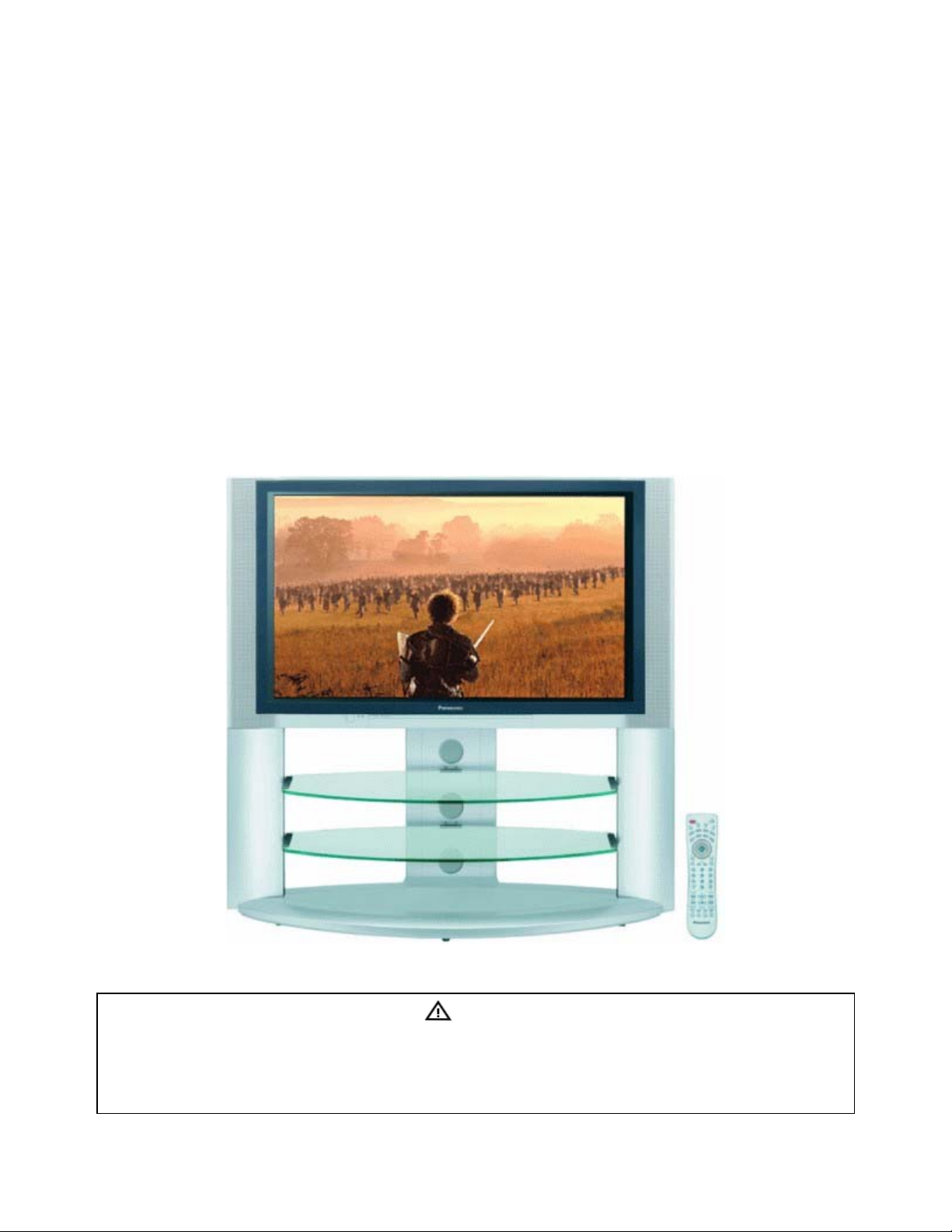
Panasonic Services Company
National Training
TH-42PX20U/TH-50PX20U
TH-42PA20U/TH-37PA20U
Plasma Display Panel
GP6D Chassis
Update Information
This service information is designed for experienced repair technicians only and is not designed for use by the general public. It does
not contain warnings or cautions to advise non-technical individuals of potential dangers in attempting to service a product. Products
powered by electricity should be serviced or repaired only by experienced professional technicians. Any attempt to service or repair
the product or products dealt with in this service information by anyone else could result in serious injury or death.
1
Warning
Page 2

2
Page 3

Table of contents
Objective..............................................................................................................5
Model Line Up .....................................................................................................7
Performance Comparison..................................................................................8
SD Models.........................................................................................................8
HD Models ........................................................................................................8
Specifications......................................................................................................9
SD Models.........................................................................................................9
HD Models ........................................................................................................9
New Features and Circuit Improvements .......................................................10
42” SD PCB Board Layout Diagram................................................................11
Board Comparison Chart .................................................................................12
Video Signal Block Diagram ............................................................................13
Video Signal Path Explanation ........................................................................15
NTSC \ 480i Video Signal Path .......................................................................15
DVI Input.........................................................................................................17
DVI RGB to YUV Conversion..........................................................................18
Digital Processor.............................................................................................19
Main Picture ....................................................................................................19
RGB Amplifier..................................................................................................21
RGB/PC Select................................................................................................22
D Board Outline...............................................................................................23
Sync Signal Process .......................................................................................24
SC Board Explanation......................................................................................25
SS Board Explanation ......................................................................................28
Power Supplies (GP6D Chassis) .....................................................................31
Standby power supply.....................................................................................31
VSUS High Voltage Source.............................................................................32
Main Power Supply .........................................................................................34
VDA and other Voltage Sources......................................................................35
Protection Circuits............................................................................................37
System Control Circuit.....................................................................................39
Panel Operations.............................................................................................39
TV Operations.................................................................................................40
Diagnostic Procedures.....................................................................................41
Diagnostic Flow Charts....................................................................................42
No Power ........................................................................................................42
No Picture Flowchart 1....................................................................................43
No picture Flowchart 2 ....................................................................................44
Dark picture Flowchart ....................................................................................45
Local screen failure..........................................................................................46
Service Hints...................................................................................................47
Adjustments......................................................................................................52
3
Page 4

+B Set-up........................................................................................................52
Confirmation....................................................................................................52
Driver Set-up...................................................................................................53
Panel Label information...................................................................................53
Initialization Pulse Adjust.................................................................................54
P.C.B. (Printed Circuit Board) exchange procedure........................................55
Adjustment Volume Locations.........................................................................55
Test Point locations.........................................................................................56
Serviceman mode (Electronic Controls).........................................................56
Serviceman mode (Electronic Controls).........................................................57
CAT (computer aided test) Mode ....................................................................58
I2C Mode .........................................................................................................59
I2C Menu Structure..........................................................................................60
CD mode.........................................................................................................61
SD Mode .........................................................................................................62
Alignment Procedures......................................................................................63
Pedestal Setting..............................................................................................63
NTSC White Balance Adjustment....................................................................64
HD Panel White Balance Adjustment..............................................................65
Sub Brightness Setting....................................................................................66
Hotel Mode Operation.....................................................................................67
Service Contact Information............................................................................70
4
Page 5

Objective
The information provided in this document is designed to assist the technician in
determining the defective printed circuit board. The troubleshooting flow charts,
signal path charts and connector information should provide enough detail to the
technician for the accurate repair of the product. Alignment and adjustment
procedures are also included in this document.
The Block diagrams and the schematic drawings reference the model TH42PHD5, TH-42PX20U and TH-42PA20U but the technology is consistent with
any GPH5D and GP6D series Plasma display panels.
5
Page 6

6
Page 7
Model Line Up
TH-50PX20U
50-inch (127 cm) HD Version
2 Component Video Inputs
3 Composite Video Inputs
3 S-Video Inputs
1 HDMI input
Scalable PIP (1/4 to 1/16)
PC / SD Card Inputs
Integrated Speaker System
BBE sound
1080i / 480p capable
720p (PC input only)
TH-42PX20U
42-inch (106cm) HD Version
2 Component Video Inputs
3 Composite Video Inputs
3 S-Video Inputs
1 HDMI input
Scalable PIP (1/4 to 1/16)
PC / SD Card Inputs
Integrated Speaker System
BBE sound
1080i / 480p capable
720p (PC input only)
TH-42PA20U
42-inch (106 cm) SD Version
2 Component Video Inputs
3 Composite Video Inputs
3 S-Video Inputs
1 DVI input
Scalable PIP (1/4 to 1/16)
Integrated Speaker System
BBE sound
1080i / 480p capable
TH-37PA20U
37-inch (94cm) SD Version
2 Component Video Inputs
3 Composite Video Inputs
3 S-Video Inputs
1 DVI input
Scalable PIP (1/4 to 1/16)
Integrated Speaker System
BBE sound
1080i / 480p capable
7
Page 8
Performance Comparison
SD Models
Chassis GP5D GP6DU
Panel Size 42 37 42
Pixels (H x V)
Brightness
(Set)
Contrast
Gradation 1024 shades
Sharpness Good
Color Temp. 11000 11000
Power Consumption
Maximum
Standby Normal
Standby Save On
Power Off
Peak
(cd/m2)
Dark 3000:1
150 lux 140:1 120:1
852 x 480p 852 x 480p
370 370 370
295W
2.8W
1.5W
225W
2.8W
1.5W
852 x 480p
4000:1
160:1
1536 shades
Vivid
265W
1.5W
0.6W
0.4W
HD Models
Chassis GPH5D GPH6D
Panel Size 50 42 50 42
Pixels (H x V)
Brightness
(Set)
Contrast
Gradation 1024 shades
Sharpness Good
Color Temp. 11000 11000
Power Consumption
Maximum
Standby Normal
Standby Save On
Power Off
1366 x
768p
Peak
(cd/m2)
Dark 3000:1
150 lux 90:1
260 250
495W
3.0W
1.7W
1024 x
768p
225W
3.0W
1.7W
1366 x 768p 1024 x 768p
300
4000:1
160:1
1536 shades
Vivid
445W
1.5W
0.6W
0.4W
360
265W
1.5W
0.6W
0.4W
8
Page 9
Specifications
SD Models
Model Number TH-42PA20U/P
Chassis GP6DU
Panel
Power Source AC 120V 50 /60 Hz
Power Consumption 425W Standby (0.8W)
Applicable Signals NTSC
Contrast 4000:1
Dimensions (W x H x D) 1170 x 658 x 99 mm
Weight 77.2 lb (35.0 kg)
HD Models
Model Number TH-42PX20U/P
Chassis GPH6D
Panel
Power Source AC 120V 50 /60 Hz
Power Consumption 295W Standby (P. Save on) 1.8W, (P. Save Off) 0.8W
Applicable Signals NTSC
Contrast 3000:1
Dimensions (W x H x D) 1020 x 610 x 89 mm
Weight 90.4 lb (41Kg)
Screen Size SD type 42” 16 x 9 (920 x 518 mm)
Number of
Pixels
Number of Dots H 2556 x V 480
Pixel Size W 1.08 x H 1.08 mm
Drive Method AC Type Sub Field Drive System, Variable sub Field
Screen Size HD type 42” 16 x 9 (920 x 518 mm)
Number of
Pixels
Number of Dots H 3072 x V 768
Pixel Size W 0.90 x H 0.645 mm
Drive Method AC Type Sub Field Drive System, Variable sub Field
H 852 x 480 (VGA)
525i (480i), 525p (480p), 625i (575i), 625p (575p),
750p (720p), 1125 (1080)/60i, 50i, 24p, 24sf
VGA, SVGA, XGA, SXGA, UXGA
H 1024 x 768 (VGA)
Power Off 0.6W
525i (480i), 525p (480p), 625i (575i), 625p (575p),
750p (720p), 1125 (1080)/60i, 50i, 24p, 24sf, 1250
(1080)/50i
VGA, SVGA, XGA, SXGA, UXGA
9
Page 10

New Features and Circuit Improvements
Integrated NTSC Tuner
3/2 Pulldown circuit
Plasma Contrast Auto Tracking System (C.A.T.S.)
Picture-in-Picture
SD models
• New Deep Black Front Glass Filter: Improves Contrast Ratio in Lighting
Environment by 15%
• Super Real Gamma System: Reproduces 1,536 shades of gradation
(60Hz)
• 10-bit Digital Processing: Reproduces 1,070-Million Colors
• DVI Input
HD models
• New 5 Facet
Asymmetrical
Cell Structure
Panel:
Improves
Brightness
Level by 45%
• New Real Black Drive System: Achieves greater than 4000:1 Contrast
Ratio in Dark Environments
• New Deep Black Front Glass Filter: Improves Contrast Ratio in Lighting
Environment by 80%
• Super Real Gamma System: Reproduces
• 10-bit Digital Processing: Reproduces 1,070 Million Colors
• SD / PC Card Reader- View images on screen from a digital camera
• HDMI Input with Analog Audio inputs
Figure 1
1,536 shades of gradation
10
Page 11
SSiinnggllee SSccaann ((SSDD))
DDuuaall SSccaann ((HHDD))
Figure 2
•Simple and low cost circuit
•High performance
•Higher brightness
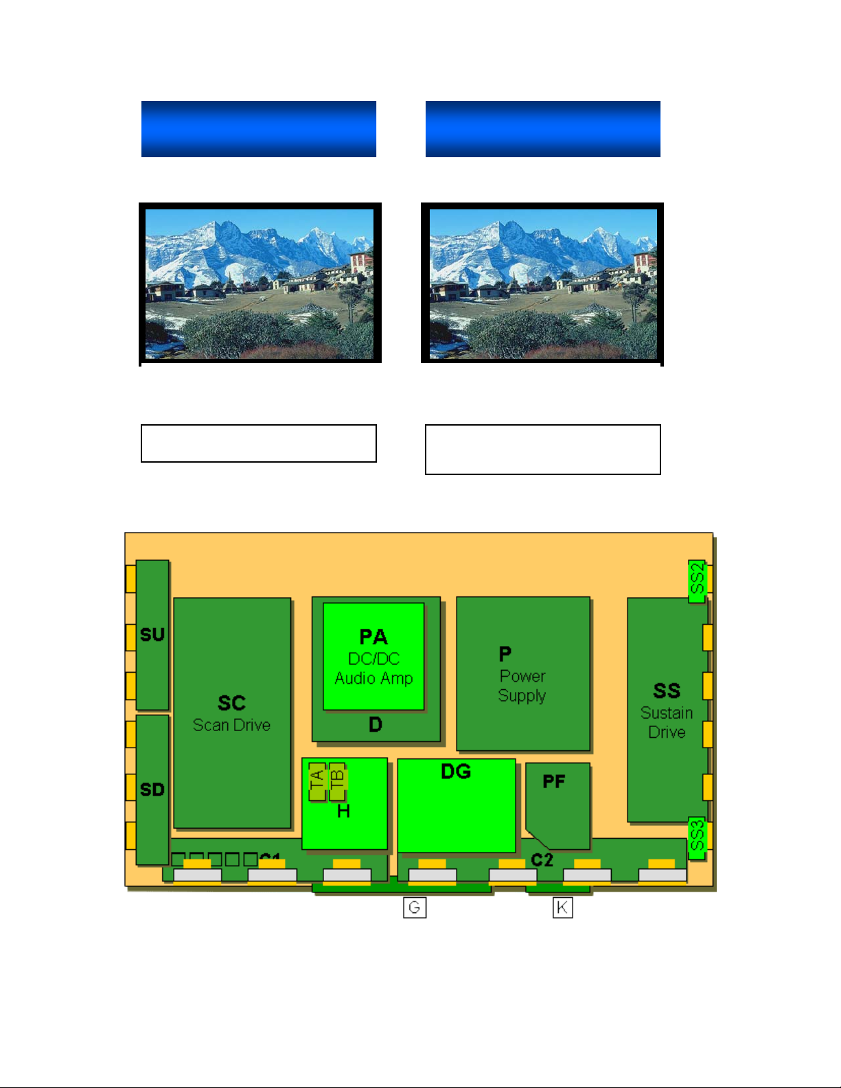
42” SD PCB Board Layout Diagram
Figure 2
11
Page 12
Printed Circuit Board Information Table
Board Name Function
PF Fuse and Line Filter Circuit
P Power Supply Circuit
PA DC/DC converter and Audio Amplifier Circuit
K Remote, Light Receiver and Power LED Circuits
G Front Switch, PC and Video Input Circuits
D RGB Digital Processor, Format converter, Plasma AI,
Discharge Control Circuits, Sub-Field Processor
SC Scan Signal Drive Circuit
SU/SD Scan Signal Output Driver (Upper and Down side)
SS Sustain Signal Output Driver
SS2, SS3 Sustain Output Signal Extension Boards
C1 Data Pulse Connector for Right
C2 Data Pulse Connector for Left
TA Tuner (main)
TB Tuner (sub)
H A/V Switching and Video Input Circuits
DG Digital Core, MPU, RGB amp, and DVI Input Circuits
Board Comparison Chart
GP5 Chassis GP6 Chassis Board Function
C1 C1 Data Drive
C2 C2 Data Drive
D2 D RGB Digital Processor, Format converter,
Plasma AI, Discharge Control Circuits, Sub-Field
Processor
D1 DG Digital Core, MPU, RGB amp, and DVI Input
Circuits
V1 G Front Switch, PC and Video Input Circuits
HX and HZ
Boards
P P Power Supply Circuit
Z PA DC/DC and Audio Circuits
F PF Fuse and Line Filter Circuit
SC SC Scan Signal Drive Circuit
SD SD Scan Signal Output Driver (Lower Section)
SS SS Sustain Signal Output Driver
SS2 SS2 Sustain Output Signal Upper Boards
SS3 SS3 Sustain Output Signal Lower Boards
SU SU Scan Signal Output Driver (Upper Section)
N/A TA Tuner (Main)
N/A TB Tuner (Sub)
H A/V Switching and Video Input Circuits
12
Page 13
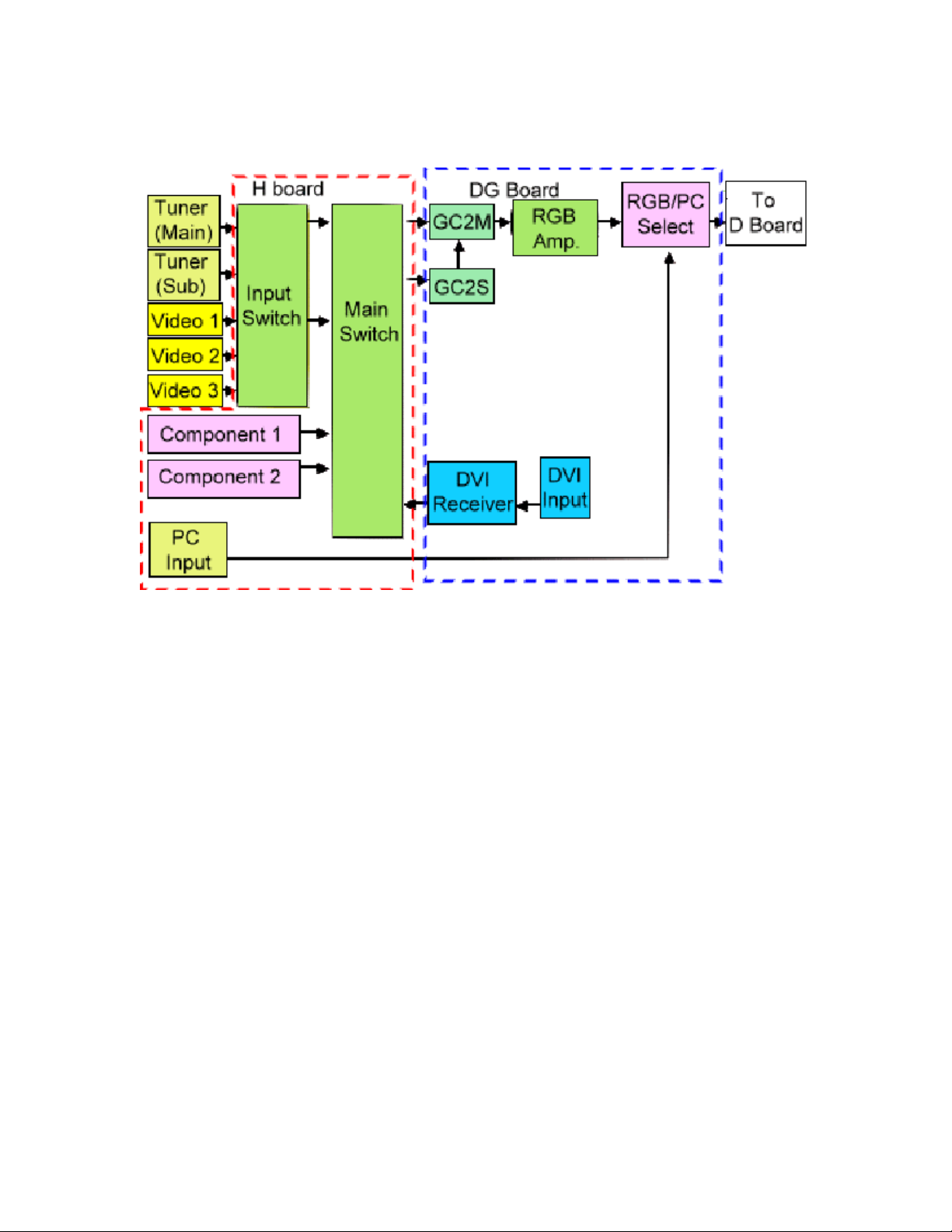
Video Signal Block Diagram
Figure 3
GP6 series plasma panels incorporate two NTSC tuners. The main tuner is used
for primary picture operation. It provides a composite video and a multiplex audio
output. The sub-tuner provides only a video output used for multi picture
functions. The video outputs of the tuners are connected to the input switch IC on
the H Board. The unit also contains three video inputs that are also connected to
the input switch IC. The input switch IC selects one of the 5 video inputs for main
picture operation and another for sub-picture operation. Selection is controlled by
2
the MPU via the I
C Bus (SDA & SCL). These two outputs are then connected to
the main switch IC.
The panel also contains three component inputs and a DVI or HDMI input
(depending upon the model) that are connected to the main switch. The DVI or
HDMI input connector, connected to the DG Board, outputs the digital signal to
the DVI or HDMI receiver where it undergoes serial to parallel conversion. The
output of the receiver is then converted to a Y, Pb, and Pr component signals
before being applied to the Main switch. The MPU selects one of the 8 inputs for
main picture operation and another for sub-picture operation.
On the DG- Board, the global core IC (GC2M) converts the composite video
signal of the main picture to RGB video signals. The GC2S IC processes the
sub-picture information and combines it with the main picture. It performs
13
Page 14

interlace to progressive scan conversion. The Global core IC also converts the
horizontal frequency of all NTSC inputs to 31.468KHz. The output of the GC2M
IC is RGB; it is applied to an external RGB amplifier.
IC001 is the TV Main CPU. It generates the On Screen Display (OSD) RGB
signals, which also enters the RGB amplifier stage. A switching circuit combines
the two sets of RGB signals for display on the screen. All NTSC, Component,
and RGB picture adjustments such as picture, tint, color, brightness, etc. are
performed inside this IC.
The RGB/PC select circuit switches between PC and all other inputs. The output
of the switch is routed to the D Board.
14
Page 15
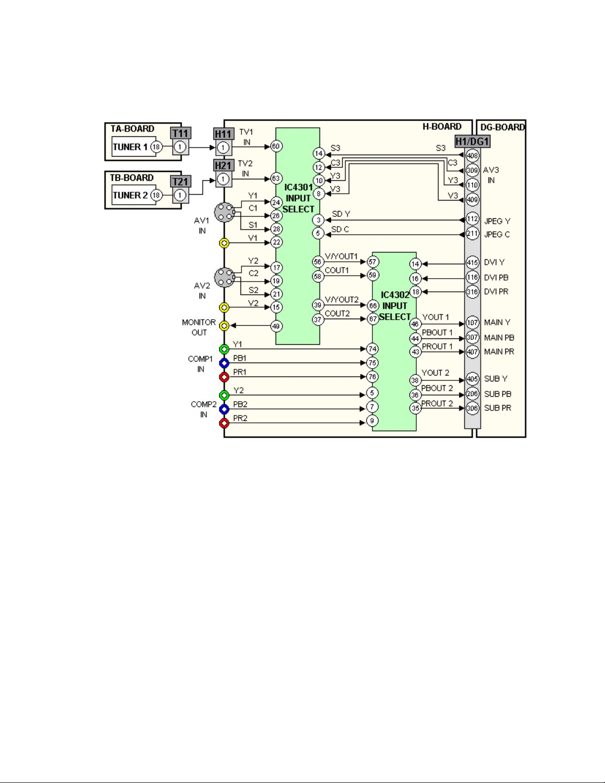
Video Signal Path Explanation
Figure 4
NTSC \ 480i Video Signal Path
The TH-42PA20U/P incorporates two NTSC tuners, allowing the simultaneous
viewing of two signals. It is also equipped with three NTSC Video inputs and
three NTSC S-Video inputs. Tuner-1 produces audio and video signals. Tuner-2
produces video only, as it is the video source intended for use in the “Picture in
Picture” mode. Video signals produced by the main tuner (tuner-1) and sub tuner
(tuner-2) are applied to the H-Board via pin 1 of the connector T11/H11 and pin 1
of the connector T21/H21. The signal applied to the AV3 video input, located at
the bottom of the front panel, enters the G-Board and passes through to the DGBoard without alteration. It is then applied to the H Board.
IC4301 on the H-Board selects the main video source and sub video source from
the NTSC inputs. The main Video or Luminance and chrominance signals are
output via pins 56 and 58. The sub video signal is output via pins 39 and 37. Both
15
Page 16

Main and Sub Video signals are amplified and applied to another video switching
IC, IC4302.
The component video signals Y, Pb, and Pr are also input to IC4302 via the
connectors located at the rear of the cabinet.
The DVI input connector, attached to the DG Board, supplies the DVI signal to
the DVI receiver where it undergoes serial to parallel conversion. The output of
the DVI receiver is converted to a Y, Pb, and Pr component signal and then
applied to pins 14, 16, and 18 of IC4302 via pins 415, 116, and 316 of connector
H1/DG1. IC4302 selects between NTSC, Component, and DVI video input
signals. The selected signals can be in any of the three formats; Video, Y/C, or Y,
Pb, Pr. The main signal is output via pins 43, 44, and 46 of IC4302. The signals
are amplified and output to the DG-Board via pins 107, 307, and 407 of the
connector H1/DG1. The Sub NTSC video signals are also amplified and output to
the DG-Board via pins 405, 206, and 406 of the same connector.
16
Page 17
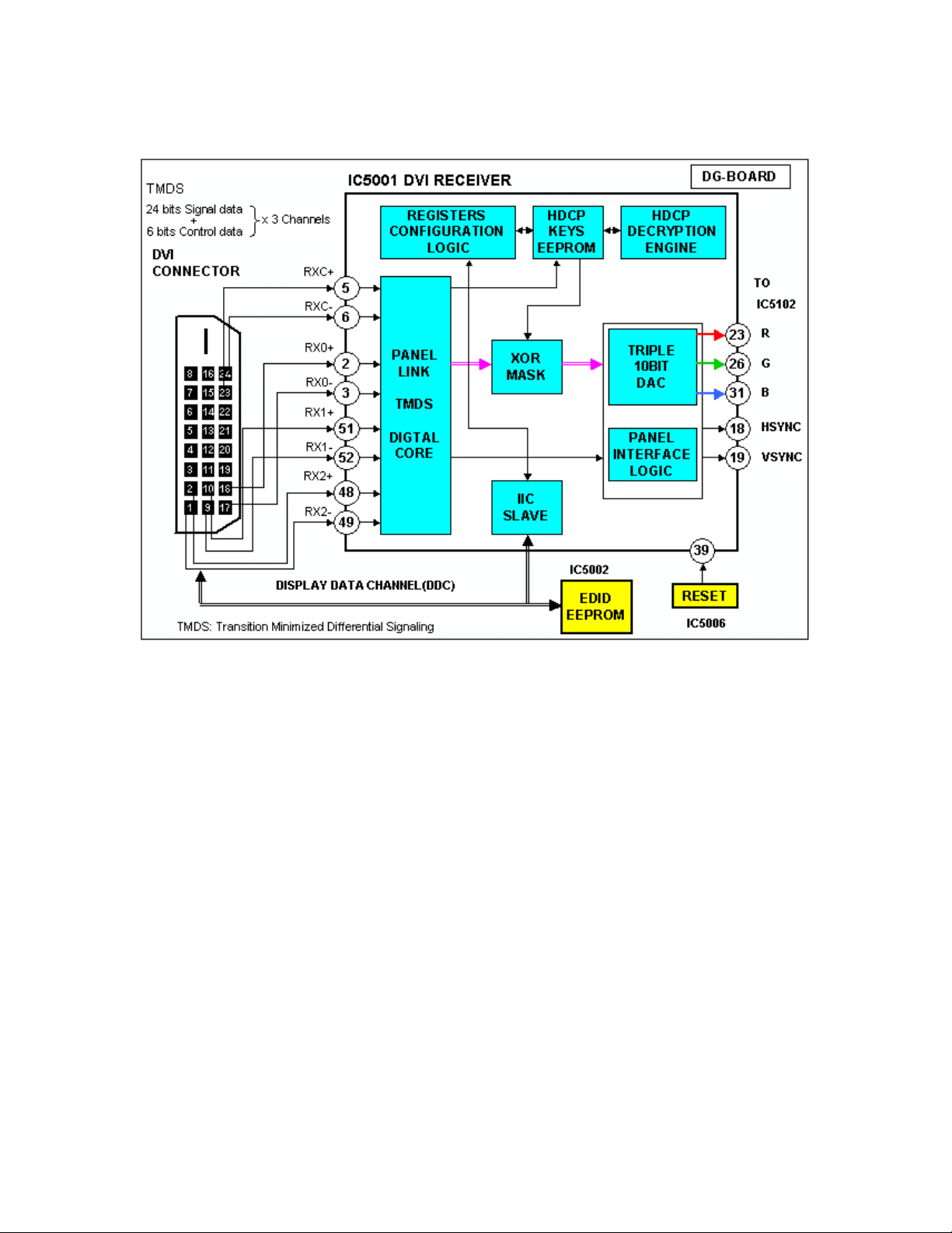
DVI Input
Figure 5
The DVI (Digital Visual Interface) input is a port designed to receive digital video
from a set-top box, a DVD player, or other digital devices. IC5001 converts the
digital video to parallel analog RGB video. The HDCP (High-bandwidth digital
content protection) circuit monitors the DVI signal for copyright protection. The
output of IC5001 is then applied to IC5102. The EDID EEPROM allows for
external control of the picture from the DVI source.
17
Page 18
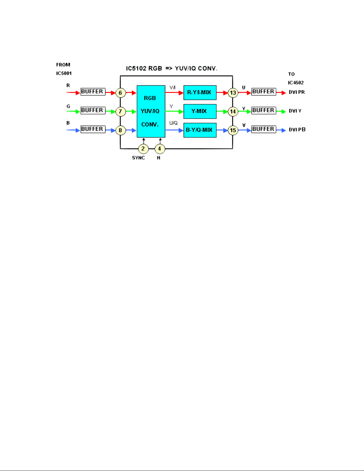
DVI RGB to YUV Conversion
Figure 6
IC5102 is an RGB to YUV (Y, Pb, PR) converter. It uses the vertical and
horizontal sync pulses of the DVI receiver to convert the analog RGB signal to Y,
Pb, Pr component signal. The signal is now in the form of an ATSC signal format
that can be processed like any other component signal. The output is sent to the
Main switch IC4302 for selection.
18
Page 19
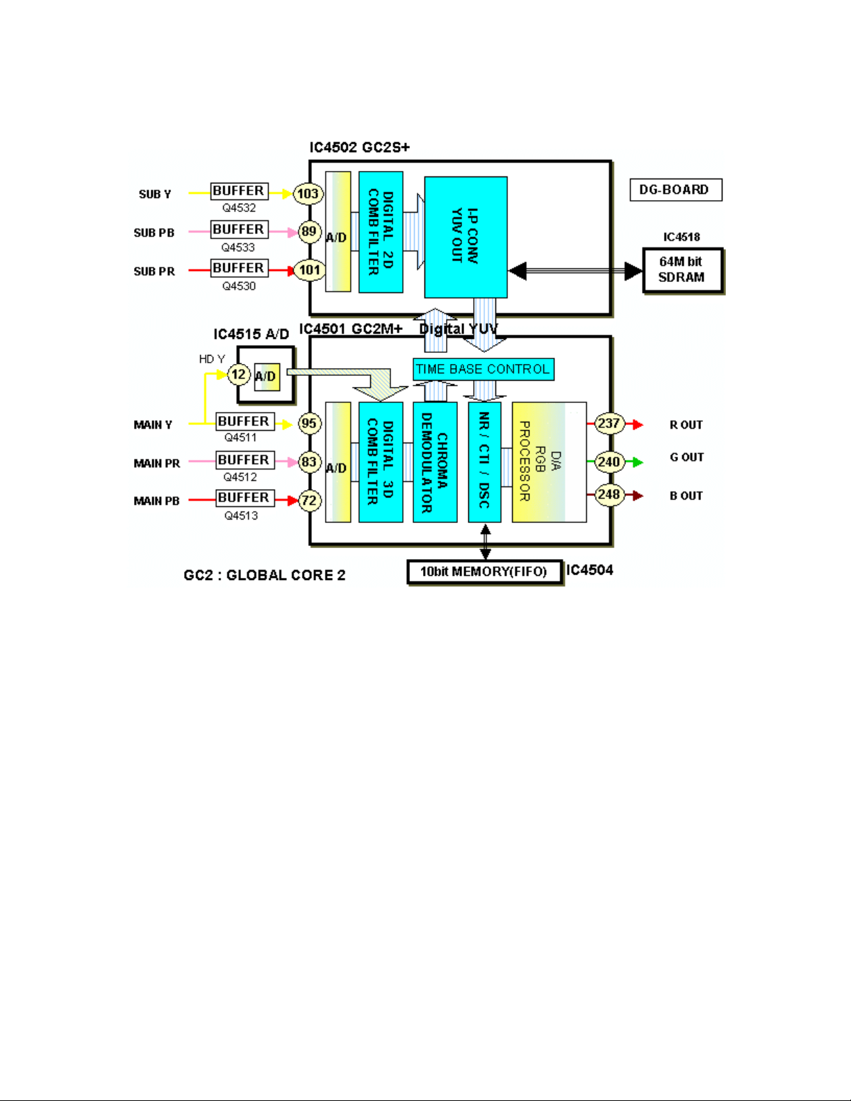
Digital Processor
Figure 7
Main Picture
On the DG- Board, the main Y, Pb, Pr signals are converted to digital data by an
analog to digital (A/D) converter circuit located inside the Global Core IC, IC4501.
The comb filter in IC4501 converts the composite video signal of the main picture
to Y and C separated video signals. S-Video, which is already Y/C separated,
simply passes through the comb filter. The data is then applied to the Chroma
demodulator circuit that separates the color signal into Pb and Pr data. If the
incoming video is in the 480p and 1080i format, the main Y signal is converted to
digital by IC4515 before being applied to IC4501. The A/D converter inside
IC4501 converts the color signals to digital. The data of the color signals bypass
the comb filter and Chroma demodulator circuits to join up with the luminance
data.
IC4501 outputs the data to the global core IC, IC4502. IC4502 contains a linedoubling circuit that halves the horizontal line period, doubling the horizontal
frequency to 31.468KHz. Using IC4518 as a temporary storage area, IC4502
19
Page 20

then converts the digital signal scan format from interlaced to progressive before
sending it back to IC4501. The NR/CTI/DSC circuit reduces noise and improves
the picture quality. The 10 bit signals are then converted to analog R, G, and B
component signals by IC4501, and applied to the RGB amplifier IC4512.
Sub Picture
On the DG- Board, an analog to digital (A/D) converter circuit, located inside the
Sub Global Core IC4502, converts the sub Y, Pb, Pr signals to digital.
The data is then applied to a comb filter where luminance and chrominance are
separated.
IC4502 processes the Sub video data for use in the PIP mode. In this mode, the
main and sub video components are combined into one set of Y, Pb, and Pr
component signals.
The line-doubler, located inside the IC, halves the horizontal line period, doubling
the horizontal frequency to 31.468KHz. Using IC4518 as a temporary storage
area, IC4502 then converts the digital signal scan format from interlaced to
progressive before sending it back to IC4501. The NR/CTI/DSC circuit reduces
noise and improves the picture quality. The 10 bit digital signal is then converted
to analog R, G, and B component signals by IC4501, and applied to the RGB
amplifier IC4512.
20
Page 21
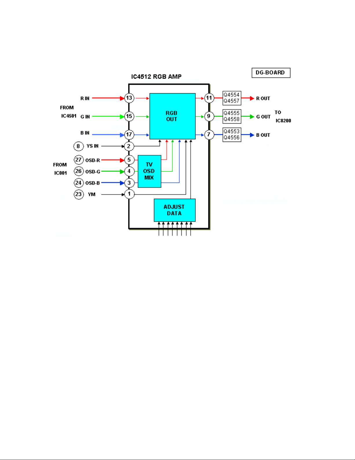
RGB Amplifier
Figure 8
The RGB output of IC4501 and the OSD (On Screen Display) RGB output of the
television MPU, IC001 enter the RGB amplifier IC4512. A switching circuit
combines the two RGB signals for display on the screen. The Adjust Data section
sets the RGB level, matching the required levels for the DG board. The output of
IC4512 enters IC8200 of the DG-Board for selection between PC and all other
inputs.
21
Page 22

RGB/PC Select
Figure 9
PC RGB Signals are input to the G Board located at the front of the unit. RGB
signals from the PC input connector as well as standard RGB signals from the
RGB amplifier, IC4512 enter IC8200 for selection. The selected output passes
through the LPF circuit consisting of IC8201 to reduce bandwidth. The filtered
output is applied to the D-Board via pins 26, 28, and 30 of the connector
DG3/D3. The output of the switch, IC8030, is used at the manufacturing plant for
testing purposes.
22
Page 23

D Board Outline
Figure 10
The D-board consists of the digital signal process circuitry. The analog RGB
input is converted to digital by IC9009. The eight bit digital output enters IC9151
for processing.
The digital video data is converted to progressive scan and mixed with the OSD
data. Adjustments such as white balance, contrast, and color drives are also
corrected here.
IC9455 contains the Plasma AI (Adaptive brightness Intensifier) circuit that
analyzes the video program level for the distribution of dark and bright
components. The Plasma AI circuit converts the 8 bit signal data to 10 bit signal
data. The Sub-field Processor is used to speed up the scanning process and
control the number of sustain periods. This increases the brightness and
improves the contrast ratio. It also creates the two channels of data that drive the
C1 and C2 data output boards.
The D-board provides the scan, sustain, and data drive signals. The scan pulses
are output to the SC board. The sustain pulses are output to the SS board. The
data drive signals are output to the C1, and C2 boards. The C1 board drives the
right portion of the panel; the C2 board drives the left portion.
23
Page 24

Sync Signal Process
Figure 11
On the DG-Board, the sync signals retrieved from the input device enter the sync
switch (IC8071). The selected sync signals are output to the D-Board via pins 31,
32, and 34 of connector DG3/D3. The sync signals then enter a level shifter IC,
IC9023, to change the DC Level from 5 to 3.3 volts. The output signals of IC9023
enter IC9009 for conversion into digital pulses. IC9605, the Sync Processor and
Discharge Control circuit, produces the Sustain control pulses, the Scan control
pulses, and the data timing pulse for the data drive circuit boards.
24
Page 25

SC Board Explanation
Figure 12
25
Page 26

Figure 13
The SC Board consists of buffers and drivers used to generate the scan signals
to the panel. The buffers provide isolation between the D board and the drivers.
Connector SC20 provides the drive voltages (140V, 100V and 18V) as well as
the trigger signals to switch the FET transistors. The D board switches the FETs
on and off to create the distinctive scan signal. Each trigger signal switches a
drive FET creating a portion of the waveform. For example, applying the CPH
signal to the 140V FET creates the peak portion of the waveform, see figure 12.
26
Page 27

Figure 14
After the scan waveform is developed on the SC Board, it is applied to the SU
and SD boards for de-multiplexing. The signal is input to a series of shift registers
inside the PDP scan driver IC. Figure 14 shows an example of the demultiplexing circuit. There are six driver ICs on the SU board and six on the SD
board.
27
Page 28

SS Board Explanation
Figure 15
After the video signal is processed on the D board, the sustain and erase pulses
are output to the SS board. The erase pulse is output at the beginning of each
scan period. The pulse is applied to the SS2 and SS3 boards to remove the
previous charge for the upper and lower sections of the display panel.
The sustain pulses are also developed on the D board and are applied after the
scan periods.
28
Page 29

Figure 16
29
Page 30

Figure 17
The Sustain pulse is developed using a similar circuit as the Scan Pulse. A series
of specifically timed pulses are applied to FET drivers creating the distinctive
sustain pulse. The drivers switch the voltages (150V, 155V and 175V) at selected
intervals determined by the D board. The basic waveform remains constant but
the exact number of sustain pulses is determined by the amount of luminance
required, see figure 17.
30
Page 31

Power Supplies (GP6D Chassis)
Standby power supply
Figure 18
The standby power supply provides the necessary DC voltage for the system
control Microprocessor, Reset circuit and the EEPROM. D404 rectifies the
incoming AC Voltage and applies it to the transformer T402 and the standby B+
control circuit IC401. The output pulses of IC401 are then applied to the primary
side of transformer T402. Diode D409 rectifies the AC output at pin 12 of the
secondary of T402 to create the STB 7V for the system control circuit. IC403
regulates the 7V standby voltage to produce the STB5V for the D Board. This 7V
standby voltage also passes through the diode D410 to enter the power relays
RL401 and RL403. When the unit is turned on, transistor Q401 turns on to create
the ground path for power relay RL401. Transistor Q417 provides the ground
path for the In Rush Current relay RL403. IC 402 and the Opto-coupler D408
provide feedback to the STB control circuit for voltage regulation. After the main
power supply goes into operation, the 5V source is applied to transistor Q402 to
turn on the relay RL402.
31
Page 32

VSUS High Voltage Source
Figure 19
The P-Board contains the drive-voltage oscillator circuit that develops the Vsus
voltage needed to operate the Scan and Sustain boards. Operation begins with
the 18Vdc supply derived at the main power supply. AC voltage from pin 4 of the
secondary of the transformer T502 is rectified filtered and applied to pin 1 of
IC550. The regulated 15 volts output of the IC enters pin 4 of IC551 to serve as
startup voltage and begin the oscillation of the IC. The regulated DC output of
IC550 is also applied to the voltage feedback circuit consisting of the optical
coupler D565 and Diode D553. The PWM output at pin 3 of IC551 is applied to
the transformer's primary. As current passes through the transformer, magnetic
field builds up in its core. The primary current passes through the transistor
located inside the IC and the four source resistors R550, R560, R568, and R574.
The voltage at the transistor's Source increases at a proportional rate to that of
32
Page 33

the current increase. This voltage is applied to the non-inverting input of the opAmp at pin 1 of IC551 for over current protection (OCP).
Pin 1 of the IC also monitors the status of the transformer. The network
consisting of D555, D551, R575, and C554 rectifies and filters the AC voltage at
pin 2 of the secondary of the transformer T501. The output voltage enters pin 1
of the IC for transformer sensing. Voltage regulation is achieved via the
feedback network consisting of D565, D553, and R557.
Figure 20A
The diodes D557and D560 rectify the AC output voltage at the secondary of the
transformer T501. The network consisting of C573, C574, R597, R598 and R600
achieves filtering. This output voltage, labeled VSUS, is applied to the Scan and
Sustain boards. Voltage regulation is achieved via the feedback circuit comprised
of the resistors R602-R606 and the Error Detect IC, IC553. The resistor R605 is
used to adjust the DC output of the circuit as indicated on the label located on the
display panel.
Note: The voltage level of the Vsus output is not mentioned because it is
different for each plasma display panel. This voltage level can be found on the
panel information label located on the heat sink of the panel.
33
Page 34

Main Power Supply
Figure 20b
Most of the DC voltages used throughout the unit are derived from this power
supply. The voltage divider circuit consisting of resistors R551, R553 and R556
reduces the output of the PFC circuit to create the startup voltage. This voltage
enters pin 4 of IC552 to begin the oscillation. The startup voltage is also applied
to the voltage feedback circuit consisting of the optical coupler D566 and Diode
D554. The PWM output at pin 3 of IC552 is applied to the primary of the
transformer T502. As current passes through the transformer, magnetic field
builds up in its core. The primary current passes through the transistor located
inside the IC and the two source resistors R569, and R576. The voltage at the
transistor's Source increases at a proportional rate to that of the current increase.
This voltage is applied to the non-inverting input of the op-Amp at pin 1 of IC552
for over-current protection (OCP).
34
Page 35

Pin 1 of the IC also monitors the status of the transformer. The network
consisting of D564, D556, R573, and C553 rectifies and filters the AC voltage at
pin 2 of the secondary of the transformer T501. The output voltage enters pin 1
of the IC for transformer sensing. Voltage regulation is achieved via the
feedback network consisting of D566, D554, and R558.
VDA and other Voltage Sources
Figure 20c
The +12V source
The 20V source is primarily used in the A-Board. It is applied to a regulator IC,
IC2304 to obtain a 9V output. The diode D568 converts the AC voltage supplied
by the secondary windings of the transformer T502 to 12Vdc.
35
Page 36

The +15V source
The 15V source is primarily used in the A-Board. It is applied to regulator IC7502
and IC7503 to obtain 9.2V and 5V output. The diode D560 rectifies the AC output
of the secondary winding of the transformer T502 to 15Vdc.
The other +12V and +5V sources
The diode D573 rectifies the AC output of the secondary windings of the
transformer T502 to 12Vdc. This voltage source is applied to the PA board and D
board of the unit. The 12V source is connected to the anode of the D566This 12V
source is also regulated by IC555 to create a 5V source that is used on the D
board.
The DR15V source
The diode D574 converts the AC output of the secondary windings of the
transformer T502 to DR15V. This voltage source is applied to the SC and SS
boards for Scan and Sustain operations. The PA board and fan control circuit
also uses the DR15 voltage source.
The VDA voltage source
Pin 11 of the secondary of the transformer supplies the VDA voltage for use on
the SS Board. This voltage is tied to a regenerative (power save circuit) that
rectifies the voltage as well as controls the output. It monitors and controls the
current used by the SS Board to achieve lower power consumption. The VDA
source is also connected to the voltage feedback circuit consisting of IC557 and
the optical coupler D558. It is the voltage source that is monitored to control the
voltage output of this power supply.
36
Page 37

Protection Circuits
Figure 21
Protection circuits are incorporated in the unit to prevent the failure of a single
circuit or component from creating catastrophic damage.
Transistor Q7541 monitors the UNR21V, UNR14V, +9(S)V, and +5(S)V line. If
any of these supply lines develop a short circuit, transistor Q7541 goes into
conduction and applies a high to pin 69 of the MPU, IC001, triggering an SOS
condition.
Transistor Q7544 monitors the +3.3V, and +2.5V line. If any of these supply lines
increase in voltage transistor Q7544 goes into conduction causing its collector to
go low. As a result, Q7541 conducts and applies a high to pin 69 of the MPU,
IC001, triggering an SOS condition.
The +9(M)V, and +2.5(M)V are also monitored for a drop in voltage. A decrease
in any of these two supply lines forces the respective diode to conduct and
trigger Q7542. A high is applied to pin 69 of the MPU, IC001, triggering an SOS
condition.
37
Page 38

The Unregulated 15V and 1.8V lines are monitored for a voltage decrease.
Under normal conditions, the voltage drop derived from the voltage divider
circuits at the base of Q9714 or Q9716 is enough to turn the transistor on.
However should the voltage drop decrease, Q9716 or Q9714 respectively, turn
off, allowing the 5 volts at their collectors to forward bias transistor Q9715. This
effectively grounds pin 3 of the CPU triggering the shutdown condition.
The four ventilation fans are monitored to be sure they are operating properly. If
one of the fans opens or increases resistance, the resulting current change is
applied to pin 37 of the main CPU.
The Scan and Sustain voltages on the SC and SS boards are monitored in a
similar manner. The +15V Line on the SS board is fed to a voltage divider and
the result is compared to a reference voltage. The reference voltage is provided
by a zener diode. If the output of the comparator goes high, a transistor turns on,
effectively grounding the SOS line. The SC board uses a similar circuit.
Additionally the SS and SC boards contain LED indicators to alert the technician
when a problem exists. The LED should be lit during normal operation, a dark
LED indicates that a problem exists on that board.
Pin 63 of IC9709 monitors the 170 V, 15V, and 20V lines. If any of these supply
lines develop a short circuit, the inline transistor goes out of conduction and
applies a high to pin 63 of the Sub CPU, IC9709, triggering an SOS condition.
38
Page 39

System Control Circuit
Panel Operations
Figure 22
This main CPU, IC9701 uses three different I2C bus lines to control peripheral
devices. Bus line 1 controls the operation of the EEPROM. Programmable setting
such as drive settings or white balance is stored in the EEPROM, IC9702. Bus
line 2 controls the video processing, main tuner and the sub tuner. Examples of
video processing include on-screen display, tint or contrast as well as many other
picture adjustments. Bus line 3 reads the data from the Stand-by CPU for front
panel and remote control operation. Additionally bus line 3 reads the condition of
the SOS protection lines and transfers this information to the Main CPU.
In all cases, the Main CPU, is the master of the bus, all other devices are slaves.
This means that all commands are generated from the Main CPU.
39
Page 40

TV Operations
Figure 23
IC001 acts as the TV microprocessor, controlling the tuner, video and sound
functions. Information such as channel mapping or customer preferences is
2
stored in the EEPROM IC002. I
C bus lines 1 and 2 are primarily responsible for
video and audio operation. Figure 23 shows the connections to the Global core
IC’s, Tuners, AV switches, and input devices.
40
Page 41

Diagnostic Procedures
In some cases, the front panel LED will flash a pattern indicating the circuit that
has failed. Be sure to record the pattern displayed at start-up.
Number of
LED Flashes
1 Main Micro power
2 Scan
3 3.3V S0S IC9709
4 5V SOS
5 Power SOS
6 Fan Stop IC9709
7 SCAN Driver 2
9 SUS Driver
12 Tuner
LED indicators on the SS and SC boards alert the technician when a problem
exists. The LEDs should be lit during normal operation, a dark LED indicates that
a problem exists on that board.
Failed Circuit(s) Detection
Point
IC9709
STB5V
Vscan
Driver 1
Vf5
Vad
P5V
Vsus (170V)
15V
20V
½ Voltage
(Energy Recover)
½ Voltage
(Energy Recover)
Power
UNR21V
UNR14V
+2.5V(M)
+9V(M)
Vfo
+9V(S)
+5V(S)
+3.3V(M)
pin 34
IC9709
pin 64
Pin 3
IC9709
pin 2
IC9709
pin 63
pin 37
IC9709
pin 1
IC9709
pin 61
IC001 pin
69
Note Suspected
Board(s)
Voltage
too low
Voltage
too low
D Board
Voltage
down
Voltage
down
Fan
Load
over
Detect at
IC6581
Load
over
Detect at
IC6705
Voltage
down or
over
current
P Board
SC Board
P Board
P Board
SC Board
SS Board
Tuners or
PA Board or
P Board
41
Page 42

Diagnostic Flow Charts
No Power
There are three states of “No Power” indication by the power LED:
1. The power LED does not light up.
2. The power LED is green at power up. It then turns red a few seconds later
and blinks on and off.
3. The power LED is red at power up and never changes state.
The PF Board is suspected to be
Does the
power LED
turn on?
Yes
Do F900
and F901
measure
correctly?
defective.
Yes
No
Check the
P-Board.
No
Replace the defective
component.
42
Page 43

No Picture Flowchart 1
p
Is the On screen
Display information
Yes
Does the
problem exist on
uts?
all in
Yes
Is the SC
Board LED
illuminated?
No
SC Board is probably
defective.
No
No
Yes
Is the SS
Board LED
illuminated?
No
SS Board is
probably defective.
Yes
D Board is
probably
defective.
DG Board is probably
defective.
Does the
problem exist on
Composite
video?
Yes
H or DG Board is
probably defective.
No
Does the
problem exist
on PC/RGB
Yes
G Board is probably defective.
43
Page 44

No picture Flowchart 2
A
re the video signals
correct at the DG
Is the SC board
Is the TPSC1
Waveform incorrect?
Are the voltages at
connectors SC2 and SC23
Are the trigger signals at
connector SC20 of the SC
board correct?
The SC Board is suspected
to be defective.
board input?
YES
LED lit?
YES
YES
YES
YES
NO
Reference the H and DG board
troubleshooting charts
NO
The SC board is suspected
to be defective.
NO
The D Board is suspected to
be defective.
NO
The Power Supply is suspected
to be defective.
NO
The D Board is suspected to
be defective.
44
Page 45

Dark picture Flowchart
A
A
re the video signals
correct at the D
board LEDs lit?
Is the TPSS1
Waveform incorrect?
re the voltages at connectors
SS11 and SS12 of the SS
Are the trigger signals at
connector SS23 of the SS
board correct?
The SS Board is suspected
to be defective.
Board input?
YES
Are the SS
YES
YES
YES
YES
NO
Reference the DG Board
troubleshooting charts
NO
The SS board is suspected
to be defective.
NO
The D Board is suspected to
be defective.
NO
The Power Supply is suspected
to be defective.
NO
The D Board is suspected to
be defective.
45
Page 46

Local screen failure
The Plasma Display Panel unit may develop a failure, where the symptom is
localized in a particular area of the screen. The figure below can help localize the
circuit board that is most likely to be defective. In the example in figure 24, one
of the two boards, C2 and D is likely to be the cause.
Figure 24
46
Page 47

Service Hints
Symptom: No picture (black Screen)
Suggestion: The use of a magnifying glass can help localize the defective
printed circuit board. Use the
magnifying glass to take a close
look at the pixels of the screen.
1. If the pixels are totally dark, the
defect is most likely located in
one of the following boards:
a) SC-Board
b) SU-Board
c) SD-Board
1. Check the status of the LED located on the SC-Board; if the LED is dark, a
malfunction of the SC-Board is suspected.
2. Listen to the buzz noise of the SC board; if the buzz noise is not present, a
malfunction of the SC-Board is suspected.
Suggestions: Check the
Scan pulse waveform at
TPSC1. (Use TPSS1 of the
SS-board to trigger the
oscilloscope.)
Verify the input signals at
connector SC2, SC23, and
SC20.
Verify that the signals of the
clock and serial data lines
from the D-board are present
at connector SC20.
Figure 25
TPSC1 TPSS1
Figure 26
47
Figure 27
Page 48

Symptom: No picture (black Screen)
Figure 28
Suggestion: The use of a magnifying glass
can help localize the defective printed circuit
board. Use the magnifying glass to take a
close look at the pixels of the screen.
If the pixels are faintly lit, the defect is most
likely located in one of the following boards:
A) SS-Board
B) SS2-Board
C) SS3-Board
1. Check the status of the LED located on
the SS-Board; if the LED is dark, a
malfunction of the SS-Board is suspected.
2. Listen to the buzz nois e of the SS-board. If the
buzz noise is not present, a malfunction of the
SS-Board is suspected.
3. Verify the input signals at connector SS23.
SS Board
Figure 29
48
Page 49

Suggestions:
Check the Scan
pulse waveform
at TPSC1 of the
SC-Board. (Use
TPSS1 of the
SS-Board to
trigger the
oscilloscope.)
Proceed to
the power
sources at
connector S
and SS12.
Verify that the clock
and serial data lines
from the D-board are
check
S11,
present at connector SS23.
Figure 30
49
Page 50

Symptom: Horizontal Black Bar
(Completely dark)
Note: The use of a magnifying glass can help
localize the defective printed circuit board. Use
the magnifying glass to take a close look at the
pixels in the area of the black bar.
1 If the pixels are totally dark, the defect is
most likely located in one of the following
boards:
a) SC Board
b) SU Board (upper half of the screen only)
c) SD Board (lower half of the screen only)
2. If the pixels are dimly lit, the defect is most likely located in one of the
following boards:
a) SS Board
b) SS2 Board (upper half of the screen only)
c) SS3 Board (lower half of the screen only)
Figure 31
50
Page 51

Symptom: Vertical Black Bar
Suggestion: Since the C2 board contains
the serial to parallel converters for the
picture data that drive this portion of the
screen; the most likely cause for this defect
can be localized to the C2-Board or the D-
Board.
Symptom: Vertical Black Bar
Suggestion: Since the C1 board contains
the serial to parallel converters for the
picture data that drive this portion of the
screen; the most likely cause for this
defect can be localized to the C1-Board
or the D-Board.
Symptom: No OSD but it has video.
Suggestion: Check signal on the DG board.
Symptom: Burned image
(pattern) is visible.
Suggestion: Access the CAT
mode and activate the scroll
bar or run the set with a white
raster for at least fifteen
minutes.
Figure 32
Figure 33
Panasonic
Figure 34
51
Page 52

Adjustments
If the power supply board is replaced the following adjustments are required.
+B Set-up
Item / Preparation
• Input a 100% white signal.
• Set the picture mode to Normal and the White Balance to Normal
• Adjustments/Confirmation
Adjust and confirm the indicated test point below for the specified voltage.
Adjustment
Name Test Point Voltage Potentiometer
Vsus P11 pin 2 Vsus ± 1V R605
Vda P12 pin 1 67.0 ± 0.5V R590
Confirmation
Name Test point Voltage
15V P23 pin 1 15.4V ± 0.5V
15V P7 pin 1 15.2V ± 0.5V
12V P25 pin 1 11.8V ± 0.5V
Audio 12V P5 pin 7 12.5V ± 0.8V
5V P25 pin 5 5.1V± 0.3V
STB 5V P27 pin 4 5.0V ± 0.3V
Fan 15V P10 pin 1 15.4V ± 0.5V
Fan 5V P10 pin 4 5.1V± 0.3V
PFC C468 (+), C468 (-) 380V ± 15V
52
Page 53

Driver Set-up
A
Item / Preparation
• Input an APL 100 % white signal.
• Set the picture controls to:
Picture mode = Normal
White Balance = Cool
Aspect = 16:9
Adjustments
To perform the following adjustments, please refer to the panel information label
located on the heat sink of the panel. See Figure 35 for more information about
the panel label.
Name Test point Voltage Volume
Vsus TPVSUS
(SS-BOARD)
Vbk TPVBK
(SC-BOARD)
Ve TPVE
(SS-BOARD)
Vset TPVSET
(SC-BOARD)
Vad TPVAD
(SC-BOARD)
Vda TPVDA
(SS Board)
VSCN TPVSCN
(SC-BOARD)
Vsus ± 1V* R605
(P-BOARD)
155Vbk ± 5V R6443
(SC-BOARD)
Ve ± 1V* R6774
(SS-BOARD)
218 V ± 6V Verify Only
-90 ± 1V R6477
(SC-BOARD)
67V ± 1V R590
(P-BOARD)
Vad+118V ± 2V Verify only
* Refer to the panel label for the exact value
Panel Label information
djustment
voltage
Figure 35
53
Page 54

Initialization Pulse Adjust
Item / Preparation
• Input a Crosshatch signal.
• Set the picture mode to Normal, and White Balance to Normal
Adjustments
Adjust the indicated test point for the specified waveform. Use TPSS1 as the
trigger source.
Test point Volume Level
T1 TPSC1 (SC) R6523 (SC-Board) 20 ± 15µ Sec
T2 TPSC1 (SC) R6557 (SC-Board) 170 ± 20µ Sec
Figure 36
54
Page 55

P.C.B. (Printed Circuit Board) exchange procedure
1. Caution
Wait 1 minute for the electrolytic capacitors to discharge before removing
any PCB from the unit.
2. Quick adjustment after P.C.B. or Panel exchange
P.C.B. Item Volume Test point Voltage level
Panel All items in this table
Vsus R605 (P-Board) TPVsus (SS) Vsus ± 1V* P Board
Vda R590 (P) TPVDA (SS Board) 67V ± 1V
SC Board
SS Board Ve R6774 (SS) TPVE (SS) Ve ± 1V*
D, DG Board White Balance, Pedestal and Sub brightness for NTSC, Pal, HD, PC and 625i
*Refer to the Panel label for the exact value.
Vbk R6443 (SC) TPVBK (SC) 155V ± 5V*
Vad R6477 (SC) TPVAD (SC) -90V ± 1V*
Vset TPVSET
(SC-BOARD)
VSCN TPVSCN
(SC-BOARD)
signals
218 V ± 6V Verify Only
Vad+118V ± 2V Verify only
Adjustment Volume Locations
Figure 37
55
Page 56

Test Point locations
Figure 38
56
Page 57

Serviceman mode (Electronic Controls)
This Plasma Display television uses the I²C Bus circuitry to control functions and
replace many mechanical controls. Instead of adjusting mechanical controls
individually, many of the control functions are now performed by using “On
Screen Display Menu”. (The Serviceman Adjustment Mode.)
Note: It is suggested that the technician reads all the way through and
understand the following procedure for Entering/Exiting the Serviceman
Adjustment Mode.
Entry to Serviceman Mode:
When minor adjustments need to be done to the electronic controls, the method
of entering the serviceman mode is as follows:
Using the Remote Control:
1. Select SET-UP icon and select CABLE mode.
2. Select TIMER icon and set SLEEP time for 30 Min.
3. Press “ACTION” twice to exit menus.
4. Tune to Channel 124.
5. Adjust VOLUME to minimum (0).
6. Press VOL down on the receiver. Red “CHK” appears in the upper left
corner of the screen.
7. Select an active station.
Note: If more than 30 minutes are needed after the receiver is in the
SERVICEMAN mode, setting the TIMER back to NO can disable the Sleep
Timer.
Caution: Prolonged display of patterns WILL cause an after image retention into
the panel.
The Plasma Display receiver is now in Serviceman Mode.
• Press Power on the Remote
Control to display the
Serviceman Adjustment Menu.
• Press Power again on the
Remote Control to exit the
Serviceman Adjustment Menu.
Figure 39
57
Page 58

Exiting the Serviceman Mode:
Press the Power on the receiver (not the remote) until the receiver turns off.
The unit momentarily shuts off (for about 5 seconds); then comes back on tuned
to channel 3 with a preset level of sound.
Important note:
If the Action and Power buttons of the television are used to exit the
Serviceman mode, any programmed channels, channels caption data, and
some other user-defined settings will be erased.
Note: To access NTSC or HDTV adjustments, set the receiver’s input to the
appropriate mode (TV or HDTV).
CAT (computer aided test) Mode
CAT mode menu
CAT Panel
sys8.1
IIC Mode
CD Mode
SD Mode
MS Mode
ID Mode
Mode Function Access Button
IIC Service Alignment Action
CD
(Complete
Diagnostics)
SD (Status
Display)
MS Mode Not used ------
ID Not used ------
Software Version
Information EEPROM
Edit
MTBF Parameter Action
Mute
More than 5
seconds
How to access the CAT mode
1. Enter the servicemen mode.
2. Select the OTHER (PSRVS).
3. Press the Action button on the remote.
To exit the CAT mode, access the ID mode and switch off the main power.
58
Page 59

I2C Mode
Select the I2C mode by pressing the Up/Down button on the remote control from
the front page of the CAT menu, and then press the Action button on the
remote control.
Accessing the I
Figure 40
2
C mode?
1. Select the alignment subject by pressing the 1
or 2 buttons on the remote control.
2. Select the alignment item by pressing the 4
button on the remote control.
3. Adjust the optimum setting by pressing the
Volume Up/Down buttons on the remote
control.
The data is memorized when you exit the I
2
C mode
To exit the I2C mode, press the Recall button on the remote
control.
59
Page 60

I2C Menu Structure
The values indicated in this flowchart are sampled data.
Figure 41
60
Page 61

CD mode
A
Select the CD mode from the front page of the CAT menu by pressing the
Up/Down button on the remote control, and then press the Mute button on the
remote control for more than 5 sec.
OSD
MiCom Software version
Memory data version D
Memory data version H
Memory data change Address
Data
The software version of the EEPROM (IC9354) can be upgraded by:
1. Installing a new version IC
2. Loading the new version software from the loader tool, TZSC07036
Memory data change
Note: The data is memorized when the main power switch is pushed to the off
position.
MiCom Software Version
Memory data version D
Memory data version H
Memory data change Address
Data
ddress
Data
0.11
0.11 1
21.05
OK
8 63
78 3F
0 0
0 0
Factory
New data
Original data
Change by pressing the Up/Down
0 0
buttons on the remote control.
Change by pressing the Left/Right buttons on the
remote control.
0
0
Change by pressing the Volume
Up/Down buttons on the remote
61
Page 62

SD Mode
Select the SD mode from the front page of the CAT mode by pressing the
Up/Down button on the remote control, and then press the Action button on the
remote control.
OSD
Input command
Check
23 25 27-- -- -- -- 27 27 27
-- -- -- -- -- -- -- 28 25 25 37
Power Protect
MTBF Parameter WT PT
72 12
History of remote control command
(Factory use)
Cumulative time for power on
condition. (Unit: hour)
Number of Power On Cycles
Remote Control mode
A
B
To exit the SD mode, press the Action button on the remote control.
62
Page 63

Alignment Procedures
Pedestal Setting
Equipment required: RF Video Gray Scale Generator
Panel Settings; Picture = Normal, White Balance = Cool, Aspect Ratio = 16:9
Pattern Display:
Step 1- Access the R, G and B cutoff settings and set them to “80”.
Step 2- Under the Chroma Control setting, Set Gun off to "5" (Only green
pixels emitting).
Step 3- Access the RGB Sub Adjust, G Sub Bright setting and adjust G
Sub bright so that green pixel emission starts at black 2% area and no
emission occurs in the black 0% area.
Step 4- Under the Chroma Control setting, Set Gun off to "3". (Only blue
pixels emitting.)
Step 5- Access the RGB Sub Adjust, B Sub Bright setting and adjust B
Sub bright so that blue pixel emission starts at black 2% area and no
emission occurs in the black 0% area.
Step 6- Under the Chroma Control setting, Set Gun off to "6". (Only red
pixels emitting.)
Step 7- Access the RGB Sub Adjust, R Sub Bright setting and adjust R
Sub bright so that Red pixel emission starts at black 2% area and no
emission occurs in the black 0% area.
Step 8- Change input to PC / RGB signal. Repeat procedure (1 to 7) using
PC input signal.
Figure 42
63
Page 64

NTSC White Balance Adjustment
p
p
Equipment required: NTSC Pattern Generator, Colorimeter
Panel Settings; Picture = Standard, Color Temperature = Cool, Aspect Ratio =
16:9
Step 1- Using the Pattern generator; apply a 20
IRE Window pattern signal to the panel. Apply the
color sensor to the panel and monitor the values.
Step 2- Adjust the Sub Bright Setting to 10 cd/m
Step 3- Set the G Cutoff Setting Value to 80.
Step 4- Adjust the Red and Blue Cutoff settings to
match the values in Table 1.
Step 5- Readjust the Sub Bright setting to 10
cd/m2.
Step 6- Apply an 80 IRE window pattern signal to
the Panel.
Step 7- Set the G Drive Setting value to E8.
Step 8- Adjust the Red and Blue Drive settings to
match the values in Table 1.
Step 9- Reapply the 20 IRE pattern and 80 IRE
patterns and verify that the drive and cutoff
settings match the settings in Table 1, adjust as
necessary.
Step 10- Adjust the All Drive Settings value to FC.
Step 11- Reapply the 20 IRE pattern and verify the light settings match the
table below, adjust as necessary.
2
.
20 IRE Window
attern
80 IRE Window
attern
Table 1
Color Temperature X Y
Cool (High) 0.276 0.276
Normal (Mid) 0.288 0.296
Warm (Low) 0.313 0.329
Step 12- Press the R button then the Picture button on the remote control.
Change the color temperature to Normal. Press the R button again then
the Action button to re-access the IIC mode.
Step 13- Repeat steps 2 to 11 for Normal Color Temperature.
Step 14- Press the R button then the Picture button on the remote control.
Change the color temperature to Warm. Press the R button again then
the Action button to re-access the IIC mode.
Step 15- Repeat steps 2 to 11 for Warm Temperature.
Step 16- Change the Color temperature to Cool Mode, then re-adjust the
Sub bright value to “30”.
64
Page 65

HD Panel White Balance Adjustment
p
p
Equipment required: 720p/1080i Pattern Generator, Colorimeter
Panel Settings; Picture = Standard, Color Temperature = Cool, Aspect Ratio =
16:9
Step 1- Using the Pattern generator; apply a 20
IRE Window pattern signal to the panel. Apply the
color sensor to the panel and monitor the values.
Step 2- Adjust the Sub Bright Setting to 10 cd/m
Step 3- Set the G Cutoff Setting Value to 80.
Step 4- Adjust the Red and Blue Cutoff settings to
match the values in Table 1.
Step 5- Readjust the Sub Bright setting to 10
cd/m2.
Step 6- Apply an 80 IRE window pattern signal to
the Panel.
Step 7- Set the G Drive Setting value to E8.
Step 8- Adjust the Red and Blue Drive settings to
match the values in Table 1.
Step 9- Reapply the 20 IRE pattern and 80 IRE
patterns and verify that the drive and cutoff
settings match the settings in Table 1, adjust as
necessary.
Step 10- Adjust the All Drive Settings value to FC.
Step 11- Reapply the 20 IRE pattern and verify the light settings match the
table below, adjust as necessary.
2
.
20 IRE Window
attern
80 IRE Window
attern
Table 1
Color Temperature X Y
Cool (High) 0.276 0.276
Normal (Mid) 0.288 0.296
Warm (Low) 0.313 0.329
Step 12- Press the R button then the Picture button on the remote control.
Change the color temperature to Normal. Press the R button again then
the Action button to re-access the IIC mode.
Step 13- Repeat steps 2 to 11 for Normal Color Temperature.
Step 14- Press the R button then the Picture button on the remote control.
Change the color temperature to Warm. Press the R button again then
the Action button to re-access the IIC mode.
Step 15- Repeat steps 2 to 11 for Warm Temperature.
Step 16- Change the Color temperature to Cool Mode, then re-adjust the
Sub bright value to “30”.
65
Page 66

Sub Brightness Setting
Equipment required: NTSC grayscale pattern Generator
Panel Settings; Picture = Normal, Aspect Ratio = 16:9
Pattern Display:
Note: Adjust in a Dark room.
Step 1- Set the white balance to Cool.
Step 2- Access the All cutoff setting in service mode and adjust so that pixel
emission starts in the 2% area and there is no emission in the 0% area.
Step 3- Write down all cut off data.
Step 4- Set the white balance settings to Normal.
Step 5- Adjust all the cut off values to the same data values of the Cool mode
settings.
Step 6- Set the white balance settings to Warm.
Step 7- Adjust all the cut off values to the same data values of the Cool mode
settings.
Step 8- Change the pattern to HD and apply it to the to the component input.
Step 9- Copy PAL all cutoff data to HD Mode.
66
Page 67

Hotel Mode Operation
Hotel Mode restricts certain operation functions for use in hotels
Entry to Hotel Mode
1. Enter the Service Mode using the previously described method.
Note: Leave the set tuned to cable channel 124, changing the channel may
inhibit access to the Hotel Mode EEPROM address.
2. Press the Power button on the remote control to display the service menu.
Figure 43
3. Press and hold the MUTE button on the remote
control for a few seconds. The display will change
from the standard serviceman mode setting to the
EEPROM address / data display.
4. Press the Channel Down button of the remote or
receiver to select the EEPROM ADDRESS 1584.
5. Press the Volume Up button of the remote or
receiver to set the data at EEPROM address to 01.
Data 01 allows access to Hotel Mode, Data 00
inhibits access to and disables Hotel Mode.
6. Push the Power button of the receiver or the
remote control to hide the Serviceman mode menu
EEPROM Address /
Data Display
67
Page 68

7. Press and hold the Volume Down button
of the receiver and press the TV/Video
button of the remote control three times
within two seconds to display the Hotel
Setup menu.
Item Function Options
INITIAL INPUT The receiver
automatically selects this
input every time power is
switched on.
INITIAL VOL
LEVEL
The receiver
automatically selects this
volume level every time
power is switched on.
MAXIMUM
VOL LEVEL
Limits the maximum
Volume level
INITIAL CH The receiver
automatically selects this
channel every time power
is switched on.
BUTTON
LOCK
The receiver
automatically disables the
selected front panel
buttons of the receiver
every time power is
switched on.
Figure 44
OFF /TV /COMP1 /COMP2 /DIGITAL
/VIDEO1 /VIDEO2 /VIDEO3 /PC
/JPEG
Off: gives priority to the last input in
memory.
<Selection/Range>: OFF / 0 to 63
OFF: gives priority to the last volume
Level in memory at power off
The Initial Volume can be changed
when the unit is in the Hotel Mode.
However, priority is given to the last
volume level in memory when Initial
Volume is Off.
Note: When the Initial Vol. is larger
than the Maximum Vol. make the
Initial Vol. and Maximum Vol. the
same value.
<Range>: 0 to 63
The receiver allows the user to adjust
the volume level up to the Maximum
Vol. selected.
Note: When the Initial Vol. is larger
than the Maximum Vol. make the
Initial Vol. and Maximum Vol. the
same value.
<Selection>: OFF / 0 to 69 for TV
mode and C0 to C125 for cable mode
OFF: gives priority to the last CH in
memory at power off
<Selection>: OFF / ACTION / ALL
OFF: No button restriction
ACTION: restricts ACTION Button
selection
ALL: inhibits all button operations
68
Page 69

REMOCON
LOCK
The receiver
automatically disables the
selected keys of the
remote control every time
<Selection>: OFF / ACTION
OFF: No Restrictions
Action: Action Button on the remote is
inhibited
power is switched on.
8. Push the Power button of the receiver or the remote control to hide the
Serviceman mode menu
9. Press the Power button on the front panel to store the changes; the Hotel
mode is now active.
Note: To return the unit to normal operation, use steps 1 through 5 to change the
data at EEPROM address 1584 to 00, the Hotel mode is now disabled. All normal
user functions are restored.
69
Page 70

Service Contact Information
Panasonic
Customer
Call Center
Tech Support
Hotline
Other Numbers 1-800-833-9626 Parts Dept.
1-800-211-7262
PTV and Digital Products
1-800-743-2335 (Authorized Service Centers
only)
All Other Products
1-800-572-2672 Authorized Service Centers
only (access code required)
Fax 1-800-348-7315
1-201-392-4207 Non–authorized (limited time
access)
1-800-458-5397 Musical Instruments
1-201-392-4843 Telephone PBX Systems
1-800-414-4408 Cellular Phones
1-877-924-2473 Massage Loungers
1-201-392-4281 Commercial MWO/Hotel
Televisions
70
 Loading...