

Page 1
ORDER NO. MTNC010837A1
B5
Service Manual
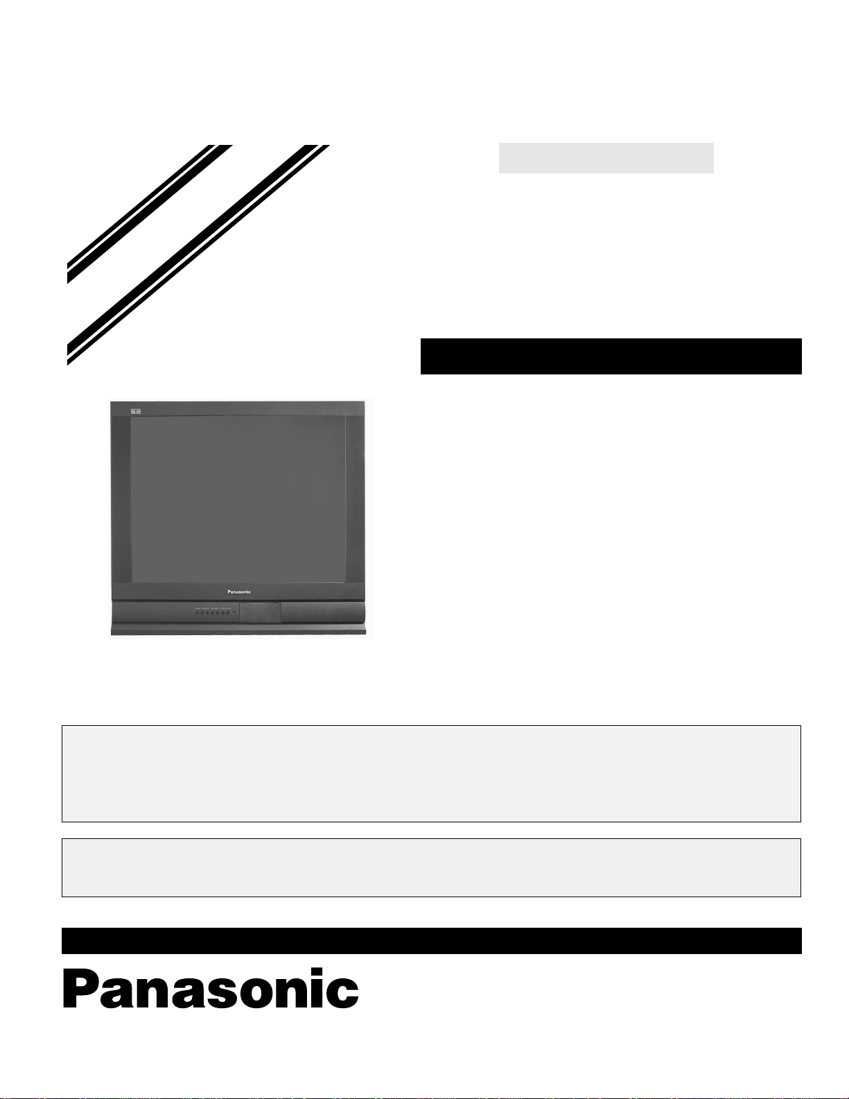
Color Television
d
e
i
S
m
i
p
l
i
f
Simplified Manual
(NA8MS)
Panasonic
Models
CT-24SX11E AP367
CT-24SX11UE AP367
CT-24SX11CE AP367
This Simplified Service Manual is issued to add listed models to the Main Service Manual order No. MTNC010527C1
(CT-27SX31E). A set of schematics, unique settings and a complete parts list are included in this Manual.
Please file and us e this Simplified Service Ma nual together with Main Serv ice Manual, order No. MTNC010527C1
(CT-27SX31E).
Chassis
“WARNING! This Service Man ual is desig ned for expe rienced repa ir technici ans only and is not designed f or use by t he general p ublic.
It does not contain warnings or cautions to advise non-technical individuals of potential dangers in attempting to service a product.
Products powered by electricity should be serviced or repaired onl y by experienced professional technicians. Any attempt to
service or repair the product or products dealt with in this Service Manual by anyone else cou ld result in serious injury or death.”
The service technician is required to read and follow the “Safety Precautions” and “Important Safety Notice” in the Ma in Ma nual.
Copyright 2001 by M atsush ita Elec tric Co rporatio n of
America. All rights reserved. Unauthorized copying
®
and distribution is a violation of law.
Page 2
Important Safety Notice
Special components are us ed in this television s et which are important for safety. These parts are identified on the
schematic diagram by the sy mbol and printed in BOLD TYPE on the replaceme nt part list. It is essenti al that
these critical parts are replaced with the manufacturer ’s specified replacement part to prevent X-ray radiation,
shock, fire or other hazards. Do not modify the original design without the manufacturer’s permission.
Safety Precautions
General Guidelines
An Isolation Transformer should always be used
during the servicing of a r eceiver whose c hassis is not
isolated from AC power line. Use a transformer of
adequate power rating a s this protects the techn ician
from accidents resulting in personal injury from
electrical shocks. It will also protec t the Receiver from
being damaged by accide ntal shorting that may occur
during servicing.
When servicing, observe the original lead dress,
especially in the high voltage circuit. Replace all
damaged parts (also parts that show signs of
overheating.)
Always Replace Protective Devices, such as
fishpaper, isolation resistors and capacitors, and
shields after servicing the Receiver. Use only
manufacturer ’s recommended rating for fuses, circu its
breakers, etc.
High potentials are present when this Receiver is
operating. Operation of the Receiver without the rear
cover introduces danger for elect rical shock. S ervicing
should not be performed by anyone who is not
thoroughly familiar with the necessary precautions
when servicing high-voltage equipment.
Extreme care should be practiced when Handling the
Picture T ube. Rough handling may cause it to implode
due to atmospheric pres sure. (14.7 lbs per sq. in.). D o
not nick or scratch the glass or subject it to any undu e
pressure. When handling, use safety goggles and
heavy gloves for protection. Discharge the picture
tube by shorting the anode to chassis ground (not to
the cabinet or to other mounting hardware). When
discharging connect cold ground (i.e. dag ground lead)
to the anode with a well insulated wire or use a
grounding probe.
Avoid prolonged exposure at close range to unshielded
areas of the picture tube to prevent exposure to
X-ray radiation.
The Test Picture Tube used for servicin g the chassis
at the bench should incorporate safety glass and
magnetic shieldi ng. The safety glass pro vide shielding
for the tube viewing area against X-ray radiation as
well as implosion. The m agnetic shield limits the X-ray
radiation around the bell of the pict ure tube in addition
to the restricting magnetic effects. When using a
picture tube test jig for service, ensure that the jig is
capable of handling 50kV without causing
X-ray radiation.
Before returning a serviced rec eiver to the owner,
the service technic ian must thoroughly test the unit to
ensure that is completely safe to operate. Do not use a
line isolation transformer when testing.
Leakage Current Cold Check
Unplug the AC cord and connect a jumper between the
two plug prongs.
Measure the resistance between the jumpered AC plug
and expose metallic parts such as screwheads,
antenna terminals, control shafts, etc. If the exposed
metallic part has a return path to the chassis, the
reading should be between 240kΩ and 5.2MΩ. If the
exposed metall ic part does not have a re turn path to
the chassis, the re adi ng sh oul d be infinite.
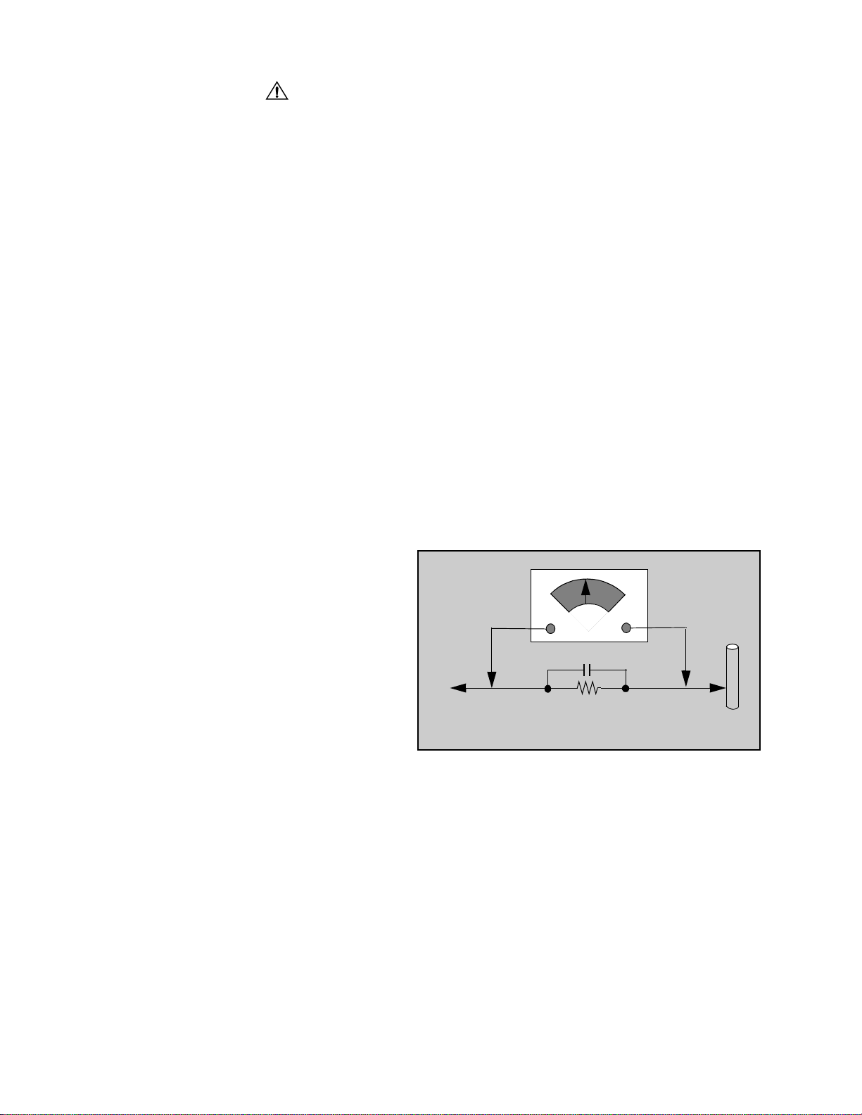
Leakage Current Hot Check (Fig. 1)
Plug the AC cord directly into the AC outlet. Do not use
an isolation transformer during the check.
Connect a 1.5kΩ 10 watt resistor in parallel with a
0.15µF capacitor between an exposed metallic part
and ground. Use earth ground, for example a
water pipe.
Using a DVM with a 1000 ohms/volt sensitivity or
higher, measure the AC potential across the resistor.
Repeat the procedure and measure the voltage
present with all other exposed metallic parts.
Verify that any potential does not exceed 0.75 volt
RMS. A leakage cu rrent te ster (such a Simp son M odel
229, Sencore Model P R57 or equiv alent) may be used
in the above procedure, in which case any current
measure must not exceed 0.5 milliamp. If any
measurement is out of the specified limits, th ere is a
possibility of a shoc k haz ar d and the Receiver mus t be
repaired and rechecked before it is returned to the
customer.
AC VOLTMETER
COLD
WATER
PIPE
(GROUND)
0.15µF
TO INSTRUMENT’S
EXPOSED METAL
PARTS
1500Ω,10 W
Figure 1. Hot Check Circuit
X-ray Radiation
WARNING: The potential source of X-ray radiation in the
TV set is in the High Voltage section and th e pictu re tube .
Note: It is important to use an accurate, calibrated
high voltage meter.
Set the brightness, picture, sharpness and color
controls to Minimum. Measure the High Voltage. The
high voltage should be 30.55 ± 1.25kV. If the upper
limit is out of tolerance, immediate service and
correction is required to insure safe operation and to
prevent the possibility of premature component failure.
- 2 -
Page 3
Important Safety Notice . . . . . . . . . . . . . . . . . . 2
Service Notes. . . . . . . . . . . . . . . . . . . . . . . . . . . 4
Board Designation Table . . . . . . . . . . . . . . . . . 4
Receiver Feature Table . . . . . . . . . . . . . . . . . . . 5
Location of Controls (Remote)
EUR511502 . . . . . . . . . . . . . . . . . . . . . . 6
Service Mode (Electronic Controls). . . . . . . . . 7
Exiting the Service Mode . . . . . . . . . . . . 7
Entering Service
Mode (Back-Open Method) . . . . . . . 7
Service Mode Regiters . . . . . . . . . . . . . . 8
Service Adjustments
(Electronic Controls). . . . . . . . . . . . . . . . . 13
Parts List . . . . . . . . . . . . . . . . . . . . . . . . . . . . . 18
Schematics, Voltages and waveforms
C-Board Voltages,
PCB & schematics . . . . . . . . . . . . . . . . . 27
A-Board Schematic
(Left Portion) . . . . . . . . . . . . . . . . . . . . . . . . 28
(Right Portion). . . . . . . . . . . . . . . . . . . . . . . 29
A-Board PCB. . . . . . . . . . . . . . . . . . . . . . . . 30
A-Board Voltages . . . . . . . . . . . . . . . . . . . . 31
P-Board schematic . . . . . . . . . . . . . . . . . . . 32
P-Board PCB & voltages. . . . . . . . . . . . . . . 33
A-Board Waveforms . . . . . . . . . . . . . . . . . . 34
Tint/Color Adjustment. . . . . . . . . . . . . . 13
Color Temperature Adjustment . . . . . . 13
Chassis adjustment procedure . . . . . . . . . . . 15
Rear View . . . . . . . . . . . . . . . . . . . . . . . . . . . . . 16
- 3 -
Page 4
Service Notes (Continued)
IMPORTANT: To protect against possible damage to
the solid state devices due to arcing or static
discharge, make certain that al l ground wires and CTR
DAG wire are securely connected.
WARNING: This Receiver has been designed to meet
or exceed applicable safety and X-ray radiation
protection as specified by government agencies and
independent testing laboratories.
CAUTION: The power supply circuit is above earth
ground and the chassis cannot be polarized. Use an
isolation transformer when servicing the Receiver to
avoid damage to the test equipment or to the chassis.
Connect the test equipment to the proper groun ( ) or
( ) when servicing, or incorrect voltages will be
measured.
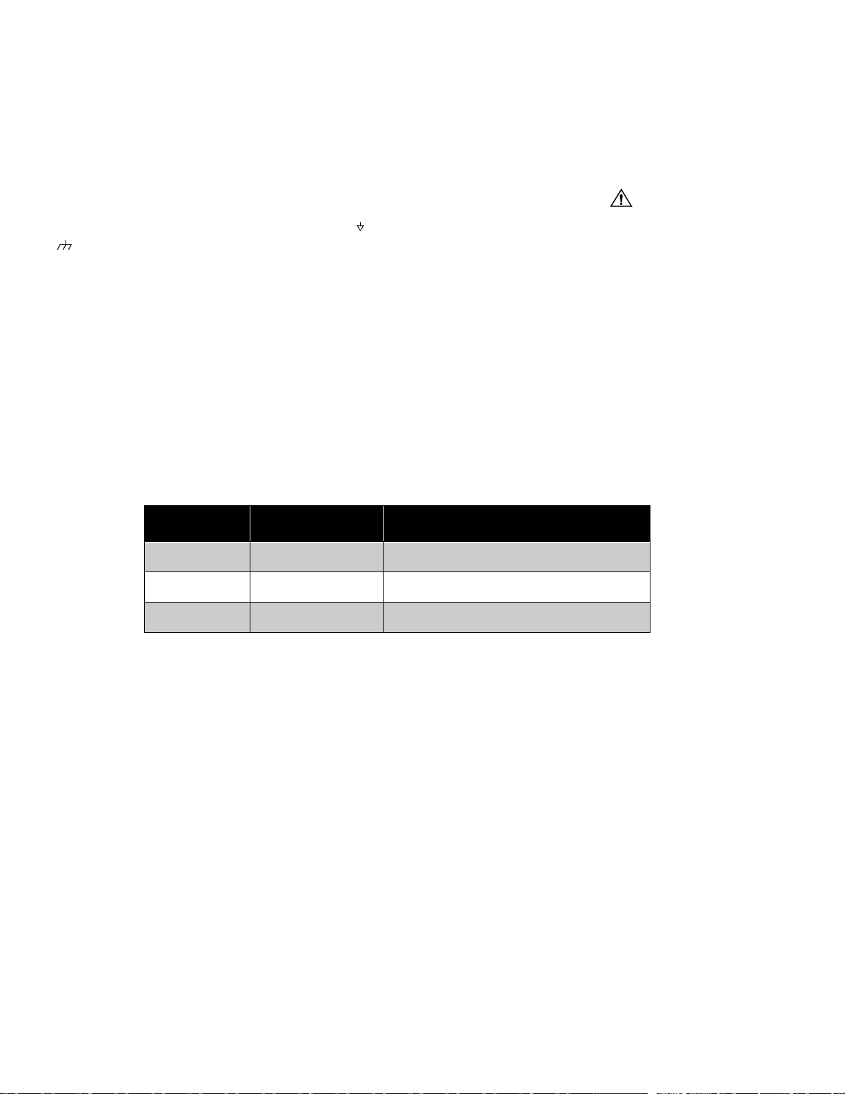
Board Table Description
BOARD PART NUMBER BOARD DESCRIPTION
A-BOARD TNP2AH025CA Main board
To maintain original product safety design standards
relative to X-ray radiation and shock and fire hazard,
parts indicated with the s ymbol on the schematic
must be replaced with identical parts. Order parts from
the manufacturer’s parts center using the parts
numbers shown in this servic e manual, or provide the
chassis number and the part reference number.
For optimum performance and reliability, all other parts
should be replaced with components of
identicalspecification.
C-BOARD TNP2AA068AF CRT panel
P-BOARD TNP2AH025CA Power Supply Board
* Note: When ordering a replacement board assembly,
append an “S” to the board number.
Example: To order the A-Board, the replacement board is
TNP2AH025CAS.
- 4 -
Page 5
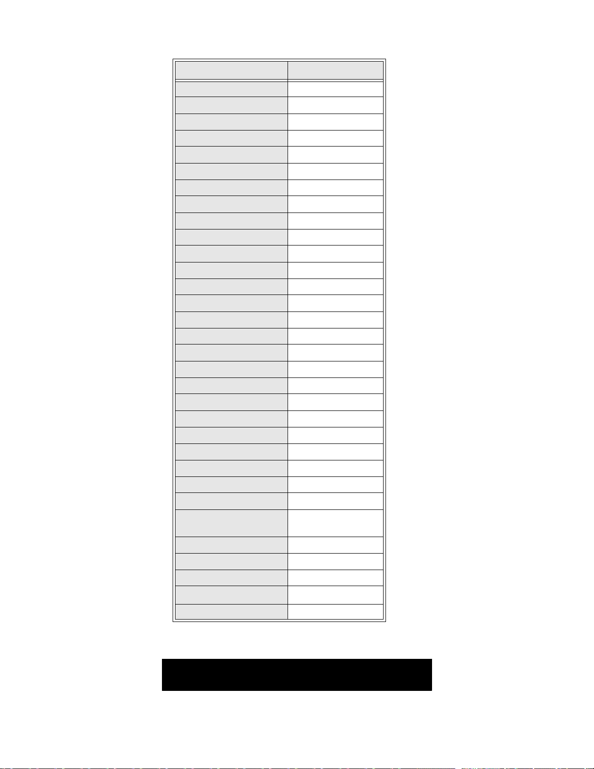
Receiver Feature Table
FEATURE/MODEL CT-24SX11E/CE/UE
Chassis AP367
Tuning system 96K
# of channels 181
Menu language Eng/Span/Fr
Closed Caption X
V-Chip X
75 Ω input X
Remote Model # EUR511502
Picture tube A60LUQ085X
PureFlat Picture Tube X
Comb Filter 3 Line Digital
V. Edge Correction X
V/A norm Both
Color Te mp. X
MTS/SAP/DBX X
Bass/Treble/Balance X
Surround Sound X
AI Sound X
Spatializer/BBE BBE
FAO & VAO X
Built-in audio power 7Wx2 (10%)
# of speakers 2
A/V in (rear/front) 3(2/1)
Component Input 1(1/0)
S-VHS Input (rear/front) 1/1
Headphone Jack X
Dimensions mm
(WxDxH) in
Weight (kg/lbs) 35/77.16
Power source (V/Hz) 120/60
Anode voltage 30.55kV ± 1.25kV
Video input jack
Audio input jack 500mV RMS 47kΩ
550x479x491.5
21.7 x 18.9 x 19.4
75Ω, phono jack
1V
p-p
Table 1. Receiver Features
Specifications are subject to change without notice or obligation.
Dimensions and weights are approximate.
- 5 -
Page 6
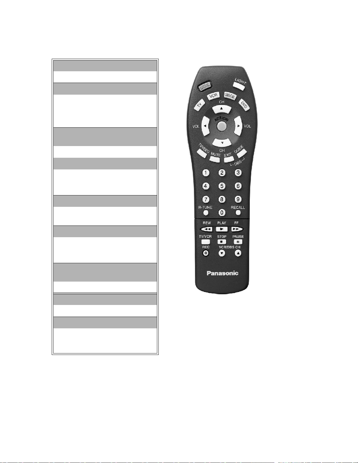
Location of Controls (Remote)
POWER Button
Press to turn ON and OFF.
MUTE Button
Press to mute sound.
A second press resumes sound.
Press also to access and delete
Closed Caption display.
VCR, DVD, LD/CD, AUX, TV, CBL,
DBS, RCVR
Component function buttons
VOL (volume) Buttons
Press to adjust TV sound level.
Use with Channel buttons to
navigate in menus.
R-TUNE (Rapid Tune) Button.
Press to switch to the previous
channel.
ACTION Button
Press to display Main Menu and
access or exit On Screen features
and Adjustment Menus.
REW, PLAY, FF, TV/VCR, STOP,
PAUSE, REC, VCR CHANNEL
Component function buttons.
TV/VIDEO Button
Press to select TV or Video input.
CH (channel) Buttons
Press to select channel s .
Use with volume buttons to
navigate in menus.
Figure 2. Location of Controls (Remote).
EUR511502
- 6 -
Page 7
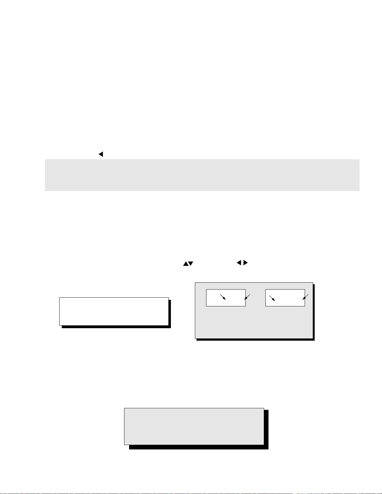
Service Mode (Electronic Controls)
This Receiver has electronic technology using the I²C Bus Concept. It performs as a control function and it
replaces many mechanical controls. Instead of adjusting mechanical controls individually, many of the control
functions are now performed by using “On Screen Display Menu”. (The Service Adjustment Mode.)
Note: It is suggested that the tec hnician reads all the way through and understand the following proced ure for
Entering/Exiting the Service Adjustment Mode; then proceed with the instructions working with the
Receiver. When becoming familiar with the procedure, the Flow Chart for Service Mode may be used as a
quick guide.
Quick Entry to Service Mode:
At times when minor a djustments need to b e done to the electroni c controls, the meth od of Entering the ser vice
Mode without removal of the cabinet back is as follows using the Remote Control:
1. Select SET-UP icon and select CABLE mode.
2. Select TIMER icon and set SLEEP time for 30 Min.
3. Press ACTION button 3 times to exit menus.
4. Tune to the Channel 124.
5. Adjust VOLUME to minimum ( 0) .
6. Press the VOL button (decrease) on Receiver. Red “CHK” appears in upper corner.
To toggle between Aging and Service modes:
While the “CHK” is displayed on the left top corner of the CRT, pressing the Action and the Volume Up buttons
on the Receiver si multaneously will toggle between the modes. Red “CHK” for Service and yellow “CHK ” for
Aging.
7. Press the Power Button on the Remote Control to select one of the Service Adjustment Modes.
1) B Service VCJ S U B-DATA ADJUSTMENT.
2) C Service VCJ CUT- O F F ADJUSTMENT.
3) D Service GEOMETRY ADJUSTMENT.
4) M Service MTS ADJUSTMENTS.
5) P Service PIP ADJUSTMENT.
6) S Service S OPTION ADJUSTMENTS.
7) X Service COMB FILTER ADJUSTMENT.
8) E Service AUDIO ADJUSTMENTS
9) “CHK” = Normal operation of CHANNEL and VOLUME .
Note: Only the appli c able settings for
b
32 B 0 2 215 C 0
a
b
a
the Receiver serviced will be
available (See
a
in Fig. 3).
An address Menu appears in the right
hand corner of the screen
Figure 3. Service Mode Menu Adjustments.
Exiting the Service Mode:
Press the Action and the Power buttons on the Receiver simultaneously for at least 2 seconds.
THE RECEIVER EXITS SERVICE MODE.
The Receiver momentarily shuts off; then comes back on tuned to channel 3 with a preset level of sound.
Any programmed channels, channels caption data and some others user defined settings will be erased.
IMPORTANT NOTE:
Always Exit the Service Mode
Following Adjustments.
- 7 -
Page 8
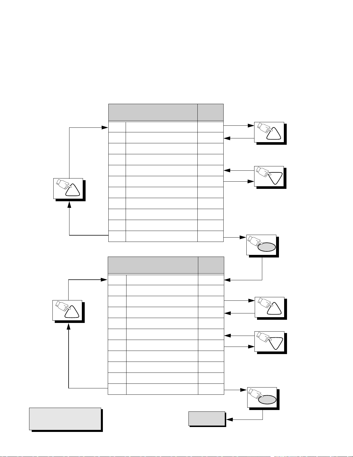
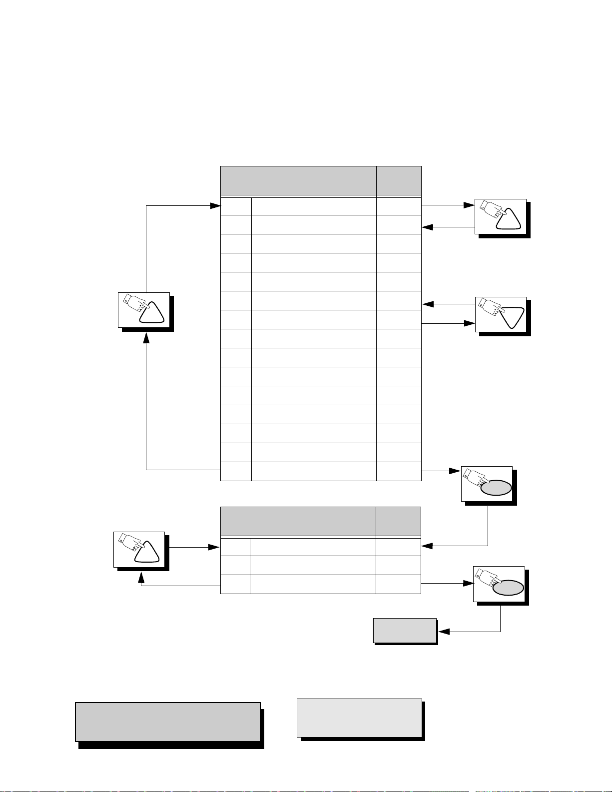
Press the Power Button on the Remote Control to select the Service Adjustment.
For Adjustments:
1.Press Channel Up/Down on the
Remote Control to select one of
the available Se rvice Adjustments
(a in Fig. 3).
Note: Write Down the original
value set (b in
Fig. 3
) for
each address before
modifying anything. It is
easy to erroneously adjust
the wrong item.
2.Press Volume Up/Down on the
Remote Control to adjust the
level of the selected Service
Adjustment (b in Fig. 3).
CH
Sub-Data Adjustment
B00 SUB-COLOR 27
B01 SUB-TINT 40
B02 SUB-BRIGHTNESS 40
B03 SUB-CONTRAST 6
B04 SUB-TINT VIDEO 10
B05 SUB-COLOR VIDEO 22
B06 SUB-TINT COMP 68
B07 SUB-COLOR COMP 28
B08 SUB SHARP TV/VIDEO 10
B09 SUB SHARP S-VHS/COMP 17
B0A SUB-CONTRAST FIXED 15
Cut-Off Adjustment
Default
Level
Default
Level
CH
CH
PW
CH
IMPORTANT NOTE:
Always Exit the S ervice Mode
Following Adjustments.
C00 CUT-OFF R 128
C01 CUT-OFF G 128
C02 CUT-OFF B 128
C03 BRIGHTNESS 31
C04 G DRIVE 64
C05 B DRIVE 64
C06 DRIVE C TEMP 8
C07 CONT C TEMP 5
C08 CUTOFF R COMP 100
C09 CUTOFF G COMP 127
C0A CUTOFF B COMP 100
To D Items.
- 8 -
CH
CH
PW
Page 9
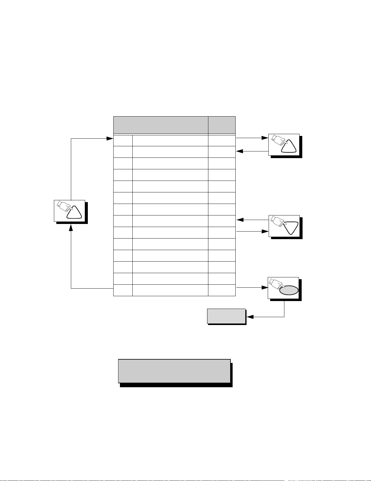
Press the Power Button on the Remote Control to select the Service Adjustment
For Adjustments:
1.Press Channel Up/Down on the
Remote Control to select one of
the available Se rvice Adjustments
(a in Fig. 3).
Note: Write Down the original
value set (b in
Fig. 3
) for
each address before
modifying anything. It is
easy to erroneously adjust
the wrong item.
2.Press Volume Up/Down on the
Remote Control to adjust the
level of the selected Service
Adjustment (b in Fig. 3).
CH
Geometry Adjustments
D00 H P OSITION 13
D01 V SIZE 37
D02 V S CORRECTION 5
D03 V LIN CORRECTION 8
D04 E/W TRAPEZIUM 9
D05 V AGC 1
D06 V POSITION 0
D07 V CENTERING 100
D08 V CENTERING DAC SW 1
D09 V-BLK START 12
D0A V-BLK STOP 14
D0B EW CORNER 3
D0C EW PARABOLA 13
D0D H WIDTH 26
Default
Level
CH
CH
D0E OSD POSITION 65
CH
Note: Some adjustment modes may not be
available in some formats.
M00 INPUT LEVEL 33
M01 LOW-LEVEL SEPARATION 6
M02 HIGH-LEVEL SEPARATION 25
MTS Adjustment
IMPORTANT NOTE:
Always Exit the Service Mode
Following Adjustments.
PW
Default
Level
PW
To P Items.
- 9 -
Page 10
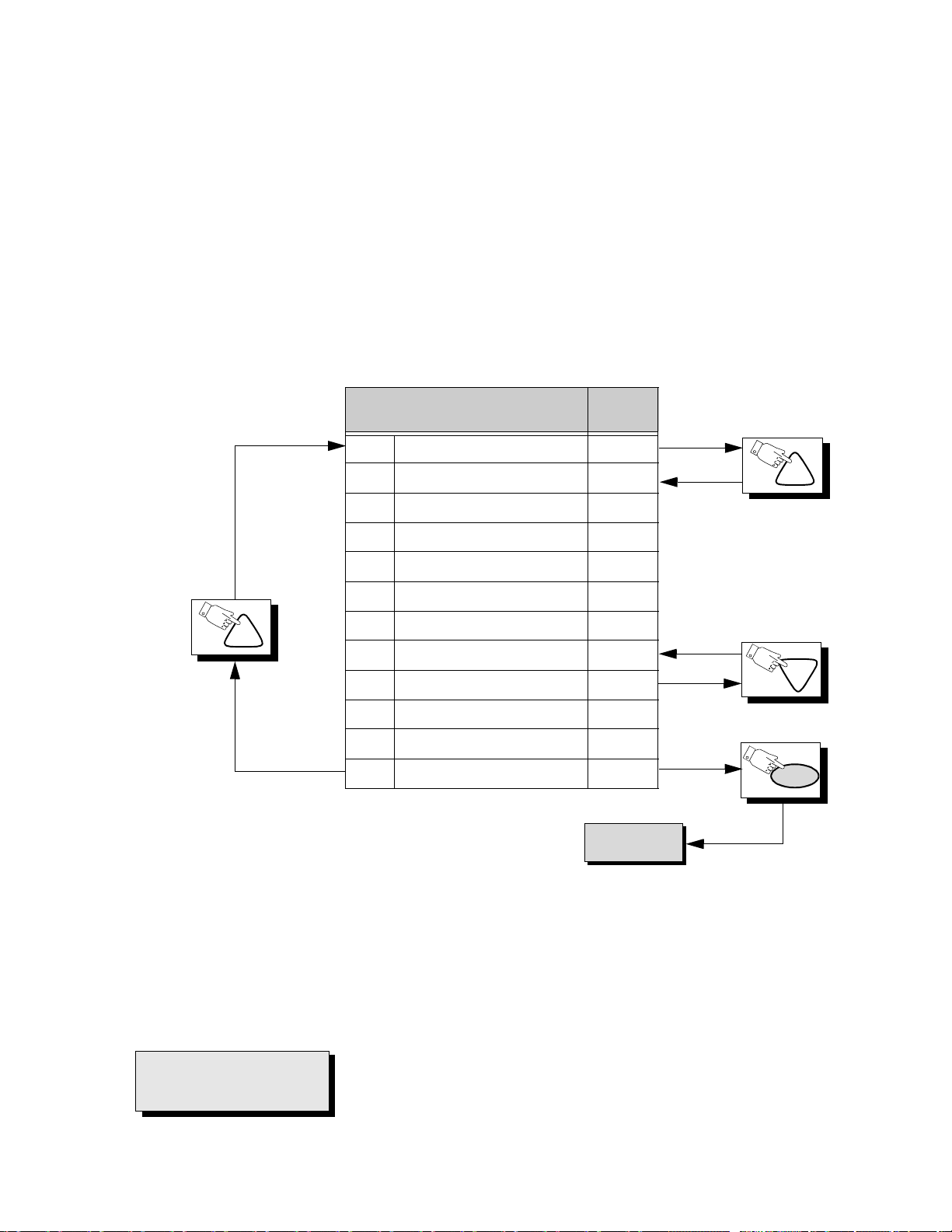
Press the Power Button on the Remote Control to select the Service Adjustment
e
e
e
For Adjustments:
1.Press Channel Up/Down on the
Remote Control to select one of
the available Servic e Adjustments
(a in Fig.3).
CH
Note: Write Down the original
value set (b in
Fig. 3
) for
each address before
modifying anything. It is
easy to erroneously adjust
the wrong item.
PIP Adjustment
P00 PIP COLOR 53
P01 PIP TINT 54
P02 PIP BRIGHTNESS 11
P03 PIP CONTRAST 58
P04 PIP POS V_TOP 26
P05 PIP POS V_BOTTOM 143
P06 PIP POS H_LEFT 10
P07 PIP POS H_RIGHT 101
P08 PIP POS 26
Default
Level
2.Press Volume Up/Down on th
Remote Control to adjust th
level of the selected Servic
Adjustment (b in Fig. 3).
CH
CH
P09 PIP POS 160
P0A PIP POS 10
P0B PIP POS 116
P0C N/A N/A
P0D PIP YDELAY 4
To S Items.
Note: Some adjustment modes may not be
available in some formats.
PW
- 10 -
Page 11
Press the Power Button on the Remote Control to select the Service Adjustment
e
e
e
For
Adjustments:
1.Press Channel Up/Down on the
Remote Control to select one of
the available Servic e Adjustments
(a in Fig.3).
Note: Write Down the original
value set (b in
Fig. 3
) for
each address before
modifying anything. It is
easy to erroneously adjust
the wrong item.
2.Press Volume Up/Down on th
Remote Control to adjust th
level of the selected Servic
Adjustment (b in Fig. 3).
CH
OPTIONS Adjustment
S00 ABL GAIN 3
S01 ABL POINT 3
S02 RGB BRIGHTNESS 6
S03 RGB GAMMA 1
S04 GAMMA 1
S05 VSM-G 0
S06 BS POINT 3
S07 CLOCK ADJUST 128
S08 CAP DIGITAL FIL 0
S09 CAP SCROLL 1
S0A RGB MATRIX 6
S0B RGB MATRIX YUV 5
Default
Level
To X Items.
CH
CH
PW
IMPORTANT NOTE:
Always Exit the Service Mode
Following Adjustme nts.
- 11 -
Page 12
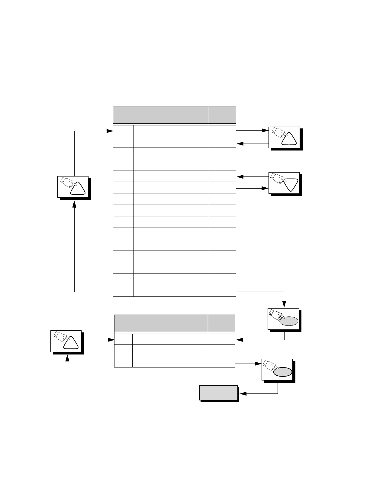
Press the Power Button on the Remote Control to select the Service Adjustment
For Adjustments:
1.Press Channel Up/Down on the
Remote Control to select one of
the available Se rvice Adjustments
(a in Fig. 3).
Note: Write Down the original
value set (b in
Fig. 3
) for
each address before
modifying anything. It is
easy to erroneously adjust
the wrong item.
2.Press Volume Up/Down on the
Remote Control to adjust the
level of the selected Service
Adjustment (b in Fig. 3).
CH
X Option Adjustment
X00 V ENHANCER 3
X01 V ENH NL 1
X02 H PEAKING GAIN 2
X03 V CORING 1
X04 C TRAP GAIN 0
X05 GEO MAG CEN 179
X06 GEO MAG GAIN 10
X07 H LOCK 1
X08 H LOCK L 70
X09 H SEPA 1L 313
X0A H SEPA 2L 266
X0B H LOCK W 0
X0C H LOCK L 70
X0D H SEPA 1WL 313
Default
Level
CH
CH
CH
X0E H SEPA 2WL 266
E Option Adjustment
E00 SURROUND EFFECT 3
E01 BBE LOW 12
E02 BBE HIGH 6
Default
Level
To B Items.
- 12 -
PW
PW
Page 13
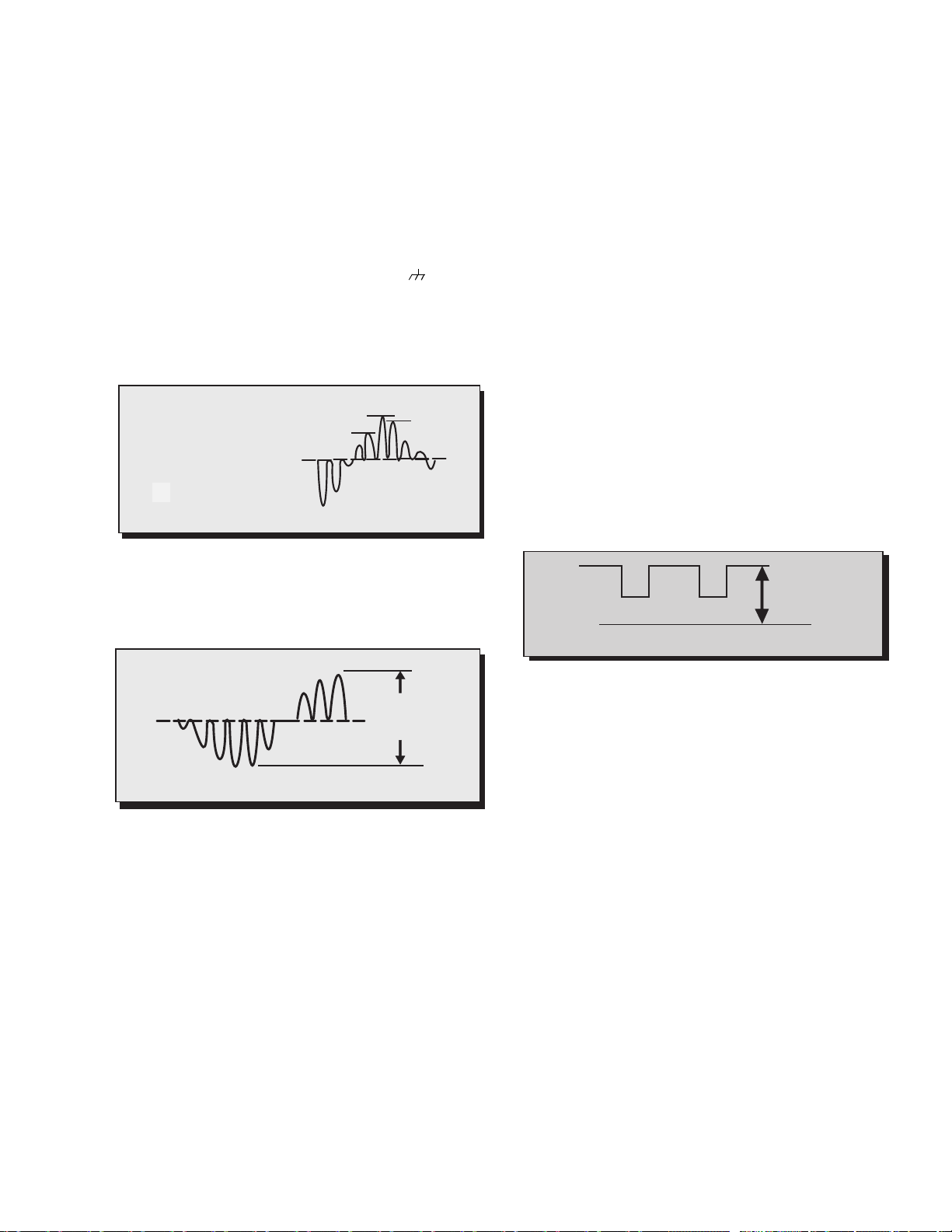
Tint/Color Adjustment
Service DAC Adjustment (B01) (B00)
Preparation:
1. Apply a rainbow color bar signal.
2. Preset the following controls:
• Brightness . . . . . . . .Min.
• Color . . . . . . . . . . . .Center.
• Tint. . . . . . . . . . . . . .Center.
• Picture . . . . . . . . . . .Max.
• Sharpness . . . . . . . .Min.
3. Set RGB GAMMA (S03) DAC to 0
4. Connect a jumper from TPD2 to GND ( ).
Procedure:
1. Connect the oscilloscope to TP47B (A-Board).
2. In the Service Mode, select (B01) DAC Sub-Tint
Adjustment. Adjust until the waveform measured is
as the one shown in Fig. 25.
TP47B (A-Board)
A to B = 1 unit
B to C = 2 units
A
A
C
1 2 3 10
4 5 6 7 8 9
B
Figure 4. TP47B waveform
3. Connect the oscilloscope to TP47R (TPL1) and
cold GND.
4. Select DAC Sub-Color Adjustment (B00) and
adjust for peak to peak amplitude to be
0.95Vp-p ±0.1V as shown in Fig. 26.
TP47G (A-Board)
1 2 3 4 5 6
7 8 9 10
0.95Vp-p±0.1V
Figure 5. TP47R waveform
Remove short jumper and set RGB GAMMA (S03)
DAC to 1.
Color Temperature Adjustment
(B/W Tracking)
Service DAC Adjust.
(C00) (C01) (C02) (C04) (C05)
Minor Touch-Up Method
OBSERVE low and high brightness areas of a B/W
picture for proper tracking. Adjust only as required for
“good gray scale and warm hi ghl ights”.
1. LOW LIGHT areas – In Ser vice Mode for making
electronic adjustments, select Cutoff (C00) RED,
(C01) GRN, (C02) BLU and adjust the picture for
gray.
2. HIGH LIGHT areas – In Service Mod e for making
electronic adjustments, select Drive (C04) GRN,
(C05) BLU and adjust the picture for warm whites.
Complete Adjustment
Preparation:
1. Turn the Receiver “ON” and allow 30 minutes
warm up at high brightness.
2. Apply a color bar signal with color “OFF”.
3. Turn the SCREEN control (part of FBT T551) fully
counterclockwis e.
Procedure:
Preset the following Se rv i ce DACs for best results:
• C0 . . . . . . . . . . . . . .128
• C1 . . . . . . . . . . . . . 128
• C2 . . . . . . . . . . . . . .128
• C4 . . . . . . . . . . . . . . 64
• C5 . . . . . . . . . . . . . . 64
1. Connect the oscilloscope to TPL1 (C-Board).
2. In Service Mode, select the Sub-Bright DAC (B02).
3. Press the R-Tune key on the remote.
4. Observe the oscilloscope waveform at Horizontal
rate and adjust the Service Mode Sub-Bright DAC
(B02) level until a scanning period of 2.4V ab ove
DC ground is measured, as indicated in Fig. 28.
2.4V DC
0V DC
Figure 6. TPL1 Waveform
5. Press the R-Tune key on the remote.
6. Connect the scope to RED Cathode (KR) on the
CRT-Board.
7. In the Service Mode, select the RED CUTOFF
DAC (C00).
8. Press the R-Tune key on the remote.
9. View scope trace at Horizon tal rate and adjust th e
Service Mode DAC (C00) level until a scanning
period of 170V above DC g round is measured, as
indicated in Fig. 29.
10. Press the R-Tune key on the remote.
11. Write the same C00 data to C01 and C02.
12. Press the R-Tune key on the remote.
13. Turn the Screen Control (part of FBT) slowly
clockwise until a slightly color horizontal line
appears.
14. Adju st DAC C01 and C02 until the horizontal lin e
becomes white.
- 13 -
Page 14
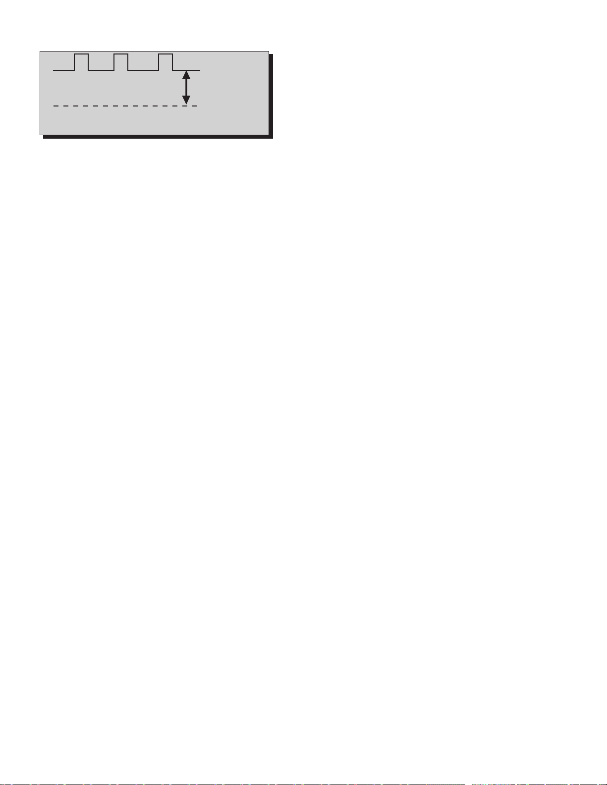
15. Press the R-Tune key on the Remote
170±2V DC
Figure 7. KR Waveform
0V DC
(Ground)
16. In the Service Mode select the DAC DRIVE
adjustments (C04) GRN, (C05) BLUE and adjust
for warm white in a white color bar pattern.
17. Apply a mon oscope pattern and check for a good
picture.
18. Perform Minor Touch-Up Method if necessary.
EXIT the Service Mode
- 14 -
Page 15
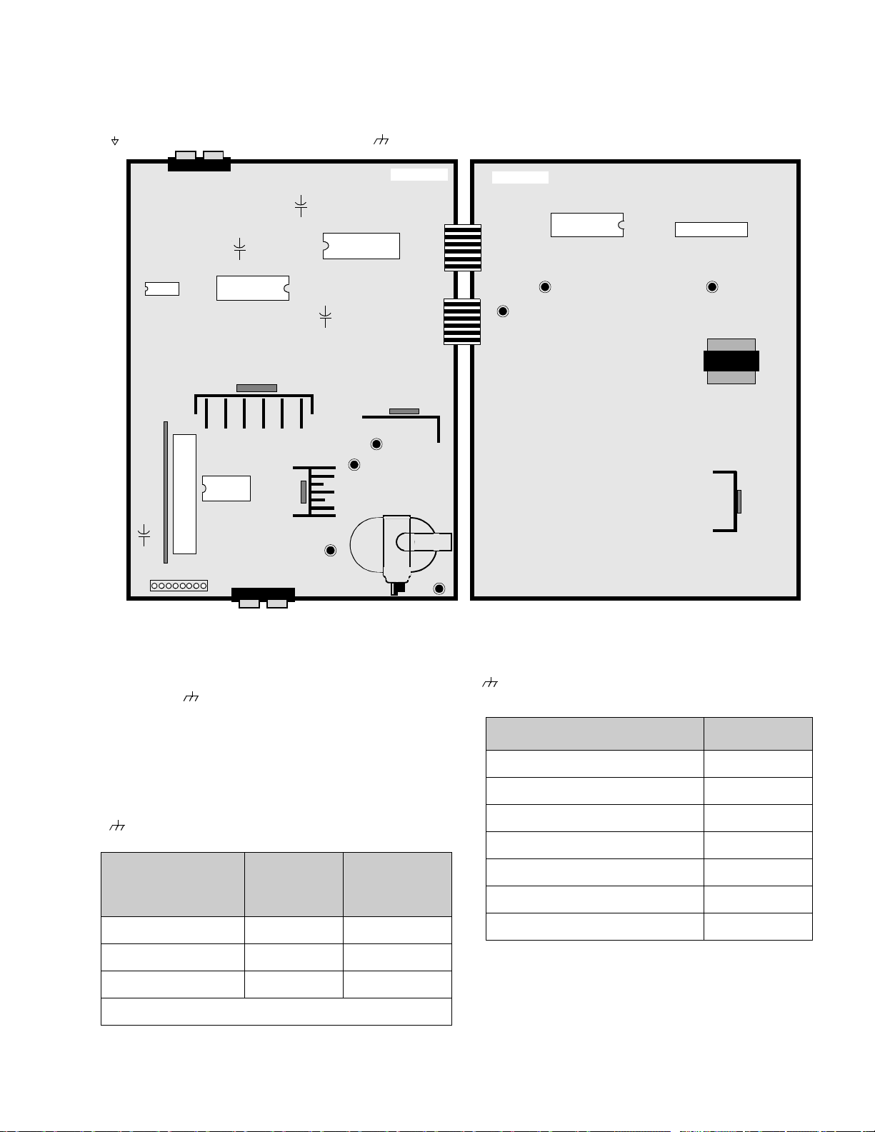
Chassis Service Adjustment Procedures
All service adjustments are factory preset and should not require adjustment unless controls and/or
associated components are re placed.
Note: Connect the (-) lead of the voltmeter to the appropriate ground. Use heat sink when the HOT ground symbol
( ) is used. Otherwise, use COLD ground ( ) — Tuner shield.
IC6501
C003
+
-
TP
T
U
IC3001
N
E
R
18
+
C584
-
IC101
IC2301
IC451
A/V REAR INPUTS
+
C583
-
+
-
TPD8
IC001
C047
TPD9
TPD3
A-BOARD
Q551
TPD7
P-BOARD
IC4802 IC4801
TPD11 TPD10
TPD12
T801
Q801
140.0V B+ Voltage Confirmation
1. Set the Bright and the Picture to Minimum by
using the Picture Menu.
2. Connect the DVM between
(+ side) and cold
TPP12
ground ( ). (In P-Board).
3. Confirm that B+ voltage is 140.0V ± 1.5V. This
voltage supplies B+ to the Horizontal Output &
Flyback circuits.
P-Board B+ Voltages
120V AC line input. Se t the Bright and the Picture to
Minimum by using th e Picture Menu. Use cold ground
) for the (-) lead of the DVM.
(
.
LOCATION
(P-Board)
VOLTAGE
Board
connected
TPP12 B+ 140.0V ± 1.5V 90.0V ± 9V
TPP11
TPP10
STBY 12
SOUND
13.0V ± 2V 8.2V ± 1V
33.0V ± 5V 25.0V ± 3V
For Sound GND use connector P1-pin 5
VOL TAGE
Board
w/o connect
A-Board B+ Voltages
120V AC line input. Set the Bright and the Picture to
Minimum by using th e Picture Menu. Use cold ground
) for the (-) lead of the DVM.
(
LOCAT ION (A-Board) VOLTAGE
C584 (+)
C583 (+)
TPD9
TPD3
TPD8
C047 (+)
TPD7
MAIN 9
MAIN 5
MAIN -15
MAIN 15
MAIN 7.5
ST-BY
MAIN 220
Adjust Picture Menu for normalized video adjustments.
9.0V ± 0.5V
5.0V ± 0.3V
-15V ± 2V
15V ± 2V
7.1V ± 1.0V
3.3V ± 0.2V
220V ± 9.0V
- 15 -
Page 16
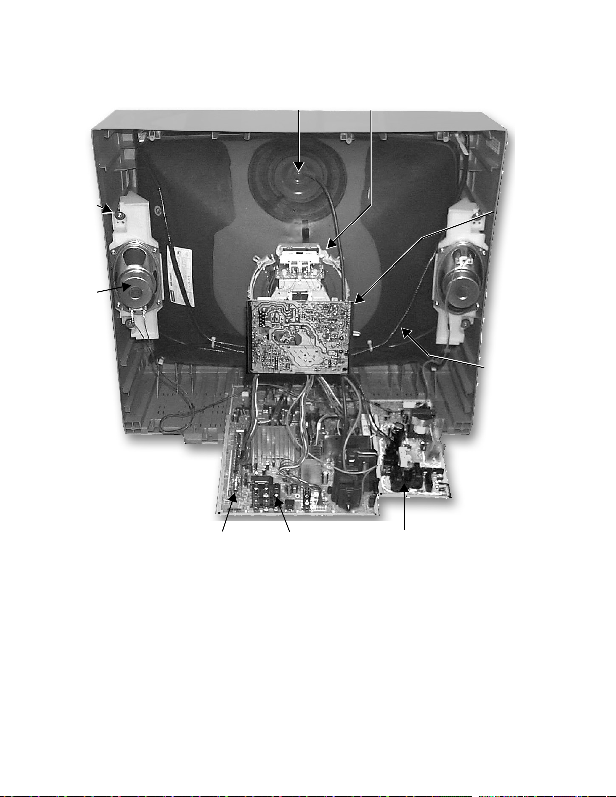
Speaker
Bracket
Speaker
Rear View
Deflection YokeCRT Anode, HV
C-Board
Tuner P-Board
Figure 8. CT-24SX11E/CE/UE Rear View
Rear AV Jacks
Degauss
Coil
- 16 -
Page 17

NOTES:
- 17 -
Page 18
REPLACEMENT PARTS LIST
Model:CT-24SX11E, CT-24SX11UE, CT-24S X11CE
Important Safety Notice: Components printed in BOLD TYPE have special characteristics important for safety. When replacing
any of these components use only manufacturer’s specified parts.
REF NO. PART NO. DESCRIPTION
CAPRISTORS
CRA801 TP00842-51 TAPING GAP TERMINAL
CRA802 TP00842-51 TAPING GAP TERMINAL
CAPACITORS
C001 ECA1CM 470B CAP,E 47UF/16V
C002 TCJ2VF1H103Z CAP,C .01UF-Z-50V
C003 ECEA1HKA4R7B CAP,E 4.7UF-50V
C005 ECA1CM470B CAP,E 47UF/16V
C006 TCJ2VF1H103Z CAP,C .01UF-Z-50V
C008 TCJ2VF1H103Z CAP,C .01UF-Z-50V
C010 TCJ2VF1H103Z CAP,C .01UF-Z-50V
C013 ECA0JM101B CAP,E 100UF-6.3V
C014 TCJ2VC1H390J CAP,C 39PF-J-50V
C015 TCJ2VC1H120J CAP,C 12PF-J-50V
C017 TCJ2VC1H270J CAP,C 27PF-J-50V
C018 TCJ2VC1H270J CAP,C 27PF-J-50V
C020 ECA0JM331B CAP,E 330UF-6.3V
C021 TCJ2VF1H103Z CAP,C .01UF-Z-50V
C024 ECA1HM4R7B CAP,E 4.7UF-50V
C025 ECA1HM010B CAP,E 1UF-50V
C026 ECA1HM010B CAP,E 1UF-50V
C032 ECA1CM331B CAP,E 330UF-16V
C033 TCJ2VC1H680J CAP,C 68PF-J-50V
C034 TCJ2VC1H680J CAP,C 68PF-J-50V
C043 ECA1HM2R2B CAP,E 2.2UF-50V
C044 TCJ2VF1H103Z CAP,C .01UF-Z-50V
C047 ECA0JM102B CAP,E 1000UF-6.3V
C048 TCJ2VF1H103Z CAP,C .01UF-Z-50V
C201 TCJ2VB1C104K CAP,C .1UF-K-16V
C224 TCJ2VB1C104K CAP,C .1UF-K-16V
C225 TCJ2VB1C104K CAP,C .1UF-K-16V
C226 TCJ2VB1C104K CAP,C .1UF-K-16V
C301 TCJ2VB1C104K CAP,C .1UF-K-16V
C302 TCJ2VB1C104K CAP,C .1UF-K-16V
C303 TCJ2VB1C104K CAP,C .1UF-K-16V
C307 ECA1HM0R1B CAP,E 0.1UF/50V
C310 TCJ2VC1H390J CAP,C 39PF-J-50V
C315 EEANA1E1R0B CAP,E 1.0UF-25V
C320 TCJ2VF1H104Z CAP,C .1UF-Z-50V
C321 TCJ2VB1H103K CAP,C .01UF-K-50V
C322 TCJ2VB1H103K CAP,C .01UF-K-50V
C323 TCJ2VB1H103K CAP,C .01UF-K-50V
C324 TCJ2VF1H104Z CAP,C .1UF-Z-50V
PARTS LIST
C330 ECA1AM101B CAP,E 100UF-10V
C331 TCJ2VF1H103Z CAP,C .01UF-Z-50V
C337 ECA1HM2R2B CAP,E 2.2UF-50V
C342 ECA1HM010B CAP,E 1UF-50V
C351 TACCV470T50V CAP,C 47PF/50V
C352 TACCV330T50V CAP,C 33PF/50V
C353 TACCV330T50V CAP,C 33PF/50V
C359 ECQM4104KZB CAP,P .10UF-K-400V
REF NO. PART NO. DESCRIPTION
C368 ECQV1H224JL3 CAP,P .22UF-J-50V
C370 ECKW3D102KBN CAP,C .001UF-K-2KVDC
C371 ECEA1HN010UB CAP,E 1UF/50V
C373 ECA2EHG100B CAP,E 10UF-250V
C377 ECA1CM221B CAP,E 10UF-16V
C401 TCJ2VB1C104K CAP,C .1UF-K-16V
C402 TCJ2VB1H102K CAP,C 1000PF-K-50V
C403 ECA1HM010B CAP,E 1UF-50V
C404 ECA1HM010B CAP,E 1UF-50V
C405 ECSF1EE105VB CAP,E 1.0UF-25V
C407 ECA1HM220B CAP,E 22UF-50V
C409 TCJ2VC1H101J CAP,C 100PF-J-50V
C410 TCJ2VB1C104K CAP,C .1UF-K-16V
C415 TCJ2VF1H104Z CAP,C .1UF-Z-50V
C453 EEUNA1E220B CAP,E 22UF-25V
C454 ECA1HHG221B CAP,E 220UF-50V
C456 ECQB1104JF3 CAP,P .10UF-J-100V
C458 ECKR1H221KB5 CAP,C 220PF-K-50V
C459 ECQB1224KF3 CAP,P .22UF-K-100V
C460 ECA1VM221B CAP,E 220UF-35V
C461 ECA1VM470B CAP,E 47UF/35V
C462 ECA1VM221B CAP,E 220UF-35V
C463 ECQB1H103JM3 CAP,P .01UF-J-50V
C465 ECA1CM101B CAP,E 100UF/16V
C470 ECQB1H104JM3 CAP,P .1UF-J-50V
C471 ECQB1H104JM3 CAP,P .1UF-J-50V
C495 ECQB1H683JM3 CAP,P .068UF-J-50V
C504 ECQB1H222JM3 CAP,P 2200PF-J-50V
C505 TCJ2VC1H180J CAP,C 18PF-J-50V
C506 ECA1CM471B CAP,E 470UF-16V
C507 TCJ2VF1H103Z CAP,C .01UF-Z-50V
C511 EC KR2H271KB5 CAP,C 270PF-K-500W
C512 EC KR2H152KB5 CAP,C .0015UF-K-500V
C514 ECA1HMR22B CAP,E .22UF-50V
C519 TCJ2VF1H104Z CAP,C .1UF-Z-50V
C535 TCJ2VC1H120J CAP,C 12PF-J-50V
C548 ECWH16103JVB CAP,P .01UF-J-1.5KV
C549 ECQM4473JZW CAP,P .047UF-J-400V
C550 ECA160V33UE CAP,E 33UF/160V
C552 ECQM6332JZW CAP,P .63UF-J-100V
C553 ECWF2754JBB CAP,M .27UF-J-200V
C554 ECKW3D102KBR CAP,C 1000PF-K-2KV
C555 ECA160V33UE CAP,E 33UF/160V
C556 ECWH20102JVY CAP,P 1000PF-J-2KV
C557 ECA1CM100B CAP,E 10UF-16V
C558 ECKW3D561JBR CAP,C 560PF-J-2KV
C559 EC KW3D681KBP CAP,C 680PF-K-2KV
C560 EC KR2H102KB5 CAP,C 1000PF-K-500V
C561 ECQB1H273JM3 CAP,M .27UF-J-50V
C562 ECKR2H471KB5 CAP,C 470PF-K-500W
C563 ECA1EM102E CAP,E 1000UF-25V
Parts List
- 18 -
201-01
Page 19
REPLACEMENT PARTS LIST
Model: CT-24SX11E, CT-24SX11UE, CT-24SX11CE
Important Safety Notice: Components printed in BOLD TYPE have special characteristics important for safety. When replacing
any of these components use only manufacturer’s specified parts.
REF NO. PART NO. DESCRIPTION
C564 EC KR2H471KB5 CAP,C 470PF-K-500W
C565 ECA1EM102E CAP,E 1000UF-25V
C566 ECKR2H471KB5 CAP,C 470PF-K-500W
C567 ECA1CM471B CAP,E 470UF-16V
C569 ECWF2304JBB CAP,M .3UF-J-200V
C570 ECA2EM220E CAP,E 22UF-250V
C571 ECKR2H102KB5 CAP,C 1000PF-K-500V
C572 ECWF2334JBB CAP,P .33UF-J-200V
C573 ECQE2474KFW CAP,P .47UF-K-200V
C580 ECA1HM4R7B CAP,E 4.7UF-50V
C581 ECA1CM471B CAP,E 470UF-16V
C582 ECA1CM101B CAP,E 100UF/16V
C583 ECA1CM100B CAP,E 10UF-16V
C593 ECEA1HNR47UB CAP,E .47UF-50V
C595 ECA1HM100B CAP,E 10UF/50V
C601 TCJ2VF1H103Z CAP,C .01UF-Z-50V
C603 EC QB 1H223JM3 CAP,P .022UF-J-50V
C616 TCJ2VB1C104K CAP,C .1UF-K-16V
C619 TCJ2VF1H103Z CAP,C .01UF-Z-50V
C628 TCJ2VC1H151J CAP,C 150PF-J-50V
C632 TCJ2VB1H103K CAP,C .01UF-K-50V
C641 ECA1CM100B CAP,E 10UF-16V
C701 TCJ2VF1H103Z CAP,C .01UF-Z-50V
C750 TCJ2VC1H181J CAP,C 180PF-J-50V
C751 ECQE 1335KFB CAP,P 3.3UF-K-100V
C752 ECA1VM470B CAP,E 47UF/35V
C753 ECQB1H222JM3 CAP,P 2200PF-J-50V
C754 TCJ2VB1H332K CAP,C .0033UF-K-50V
C755 TCJ2VB1H273K CAP,C .027UF-K-50V
C756 EC KR2H332KB5 CAP,C 3300PF-K-550V
C757 TCJ2VB1H682K CAP,C 6800PF-K-50V
C763 EC KR3A121KBP CAP,C 120PF-K -1KV
C801 EC KWAE472ZED CAP,C 4700PF-Z-500V
C802 ECKWAE472ZED CAP,C 4700PF-Z-500V
C803 EC KWAE472ZED CAP,C 4700PF-Z-500V
C804 ECKWAE472ZED CAP,C 4700PF-Z-500V
C805 EC0S2DA561BB CAP,E 560PF-200V
C806 ECQB1H104JM3 CAP,P .1UF-J-50V
C807 ECQB1H103JM3 CAP,P .01UF-J-50V
C809 EC KR3A222KBP CAP,C .0022UF-K-1KV
C812 EC QU2A224MVA CAP,P .22UF-M-250VAC
C813 ECQU2A153MVA CAP,P .015UF-M-250VAC
C814 ECQU2A153MVA CAP,P .015UF-M-250VAC
C815 ECQB1H104JM3 CAP,P .1UF-J-50V
C816 ECQB1H473JM3 CAP,P .047UF-J-50V
C817 ECQU2A224MVA CAP,P .22UF-M-250VAC
C818 ECQB1H103JM3 CAP,P .01UF-J-50V
C819 EC KCNB102MB CAP,C 1000PF-M-250V
C820 ECKCNB102MB CAP,C 1000PF-M-250V
C821 ECA1HM471E CAP,E 470UF-50V
C822 ECKR3A471KBP CAP,C 470PF-K-1KV
REF NO. PART NO. DESCRIPTION
C823 ECA1CHG101B CAP,E 100UF-16V
C824 ECKR3A821KBP CAP,C 820PF-K-1KV
C825 EEUMG2C221S CAP,E 220UF-160V
C826 ECKR3A821KBP CAP,C 820PF-K-1KV
C827 ECA1CM102B CAP,E 1000UF/16V
C828 ECKR1H471KB5 CAP,C 470PF-K-50V
C831 EC KR3A221KBP CAP,C 220PF-K-1KV
C832 EC KR3A471KBP CAP,C 470PF-K-1KV
C833 ECA1HM4R7B CAP,E 4.7UF-50V
C835 ECA1EM101B CAP,E 100UF-25V
C901 TCJ2VF1H103Z CAP,C .01UF-Z-50V
C902 TCJ2VC1H561J CAP,C 560PF-J-50V
C904 ECKR1H103ZF5 CAP,C .01UF-Z-50V
C952 ECA1HM100B CAP,E 10UF/50V
C953 ECKR1H103ZF5 CAP,C .01UF-Z-50V
C958 ECA2CM470E CAP,E 47UF-160V
C959 ECKW2H103ZF7 CAP,C .01UF-Z-500V
C960 ECCR2H151J5 CAP,C 150-500V
C961 ECA2AM100B CAP,E 10UF-100V
C962 ECKW2H103ZF7 CAP,C .01UF-Z-500V
C963 EC CR1H151J5 CAP DISC 150-5-50V
C964 ECA1CHG101B CAP,E 100UF-16V
C966 ECA1CHG101B CAP,E 100UF-16V
C967 ECA1CM221B CAP,E 10UF-16V
C968 ECKR1H103ZF5 CAP,C .01UF-Z-50V
C969 ECKR1H103ZF5 CAP,C .01UF-Z-50V
C971 TACCW222T50V CAP,C 2200PF/50V
C2202 ECA1HM2R2B CAP,E 2.2UF-50V
C2203 ECA1HM4R7B CAP,E 4.7UF-50V
C2204 AP106K016CAE CAP,T 10UF/16V
C2205 ECA1HM010B CAP,E 1UF-50V
C2206 ECQB1H223JM3 CAP,P .022UF-J-50V
C2207 AP335K016CAE CAP ,T 3.3UF/16V
C2208 TCJ2VB1C104K CAP,C .1UF-K-16V
C2209 TCJ2VB1C104K CA P,C .1UF-K-16V
C2210 TCJ2VB1C104K CAP,C .1UF-K-16V
C2211 ECA1CM100B CAP,E 10UF-16V
C2212 ECQB1H473JM3 CAP,P .047UF-J-50V
C2215 ECA0JM101B CAP,E 100UF-6.3V
C2218 ECA1HMR47B CAP,E .47UF-50V
C2220 TCJ2VC1H100D CAP,C 10PF-J-50V
C2302 ECA1HM010B CAP,E 1UF-50V
C2305 ECA1HM010B CAP,E 1UF-50V
C2307 ECA1EM102E CAP,E 1000UF-25V
C2308 ECA1HM101B CAP,E 100UF-50V
C2311 ECA1HM010B CAP,E 1UF-50V
C2312 ECA1EM102E CAP,E 1000UF-25V
C2313 ECA1VM102E CAP,E 1000UF-35V
C2314 ECA1CM101B CAP,E 100UF/16V
C2331 ECA1HM010B CAP,E 1UF-50V
C2332 ECA1HM010B CAP,E 1UF-50V
PARTS LIST
201-01
- 19 -
Parts List
Page 20
REPLACEMENT PARTS LIST
Model:CT-24SX11E, CT-24SX11UE, CT-24S X11CE
Important Safety Notice: Components printed in BOLD TYPE have special characteristics important for safety. When replacing
any of these components use only manufacturer’s specified parts.
REF NO. PART NO. DESCRIPTION
C2333 ECA1EM100B CAP,E 10UF-25V
C2334 ECA1EM100B CAP,E 10UF-25V
C2335 ECA1HM010B CAP,E 1UF-50V
C2336 ECA1HM010B CAP,E 1UF-50V
C2337 ECA1CM470B CAP,E 47UF/16V
C2431 ECA1HM010B CAP,E 1UF-50V
C2432 ECA1HM010B CAP,E 1UF-50V
C2433 TCJ2VC1H222J CAP,C 2200PF-J-50V
C2437 TCJ2VB1H333K CAP,C .033UF-K-50V
C2438 TCJ2VB1H102K CA P,C 1000PF-K-50V
C2444 TCJ2VB1C104K CAP,C .1UF-K-16V
C2445 TCJ2VB1C104K CA P,C .1UF-K-16V
C2449 TCJ2VB1H333K CAP,C .033UF-K-50V
C2450 TCJ2VB1H102K CA P,C 1000PF-K-50V
C2451 ECEA1CN100UB CAP,E 10UF-16V
C2459 TCJ2VB1H333K CA P,C .033UF-K-50V
C2460 TCJ2VB1H333K CAP,C .033UF-K-50V
C2461 ECA1HM4R7B CAP,E 4.7UF-50V
C2462 ECA1HM4R7B CAP,E 4.7UF-50V
C2463 ECEA1CN100UB CAP,E 10UF-16V
C2464 TCJ2VB1H333K CAP,C .033UF-K-50V
C2465 TCJ2VB1H333K CA P,C .033UF-K-50V
C2468 ECA1AM101B CAP,E 100UF-10V
C2473 ECA1HM4R7B CAP,E 4.7UF-50V
C2474 ECA1AM101B CAP,E 100UF-10V
C2475 ECA1HM4R7B CAP,E 4.7UF-50V
C3001 TCJ2VF1H103Z CAP,C .01UF-Z-50V
C3002 ECA1AM101B CAP,E 100UF-10V
C3003 ECA1CM100B CAP,E 10UF-16V
C3004 ECA1HM010B CAP,E 1UF-50V
C3006 ECA1HM010B CAP,E 1UF-50V
C3007 ECA1CM100B CAP,E 10UF-16V
C3008 ECA1CM100B CAP,E 10UF-16V
C3009 ECA1HM010B CAP,E 1UF-50V
C3010 TCJ2VF1H103Z CAP,C .01UF-Z-50V
C3011 ECA1HM010B CAP,E 1UF-50V
C3012 ECA1CM100B CAP,E 10UF-16V
C3013 ECA1CM100B CAP,E 10UF-16V
C3014 ECA1HM010B CAP,E 1UF-50V
C3016 ECA1HM010B CAP,E 1UF-50V
C3018 ECA1CM100B CAP,E 10UF-16V
C3019 ECA1CM100B CAP,E 10UF-16V
C3020 ECA1HM010B CAP,E 1UF-50V
PARTS LIST
C3021 TCJ2VF1H103Z CAP,C .01UF-Z-50V
C3022 ECA1HM010B CAP,E 1UF-50V
C3023 ECA1CM100B CAP,E 10UF-16V
C3024 ECA1CM100B CAP,E 10UF-16V
C3025 TCJ2VF1H103Z CAP,C .01UF-Z-50V
C6501 ECA0JM101B CAP,E 100UF-6.3V
C6502 TCJ2VF1H103Z CAP,C .01UF-Z-50V
C6503 TCJ2VF1H104Z CAP,C .1UF-Z-50V
REF NO. PART NO. DESCRIPTION
C6504 ECA1AM470B CAP,E 47UF-10V
C6505 TCJ2VF1H103Z CAP,C .01UF-Z-50V
C6506 TCJ2VF1H103Z CAP,C .01UF-Z-50V
C6507 ECA1HMR47B CAP,E .47UF-50V
C6508 TCJ2VF1H103Z CAP,C .01UF-Z-50V
C6509 ECA1CM470B CAP,E 47UF/16V
C6510 TCJ2VF1H104Z CAP,C .1UF-Z-50V
C6511 TCJ2VF1H104Z CAP,C .1UF-Z-50V
C6512 ECA1CM470B CAP,E 47UF/16V
C6513 TCJ2VF1H103Z CAP,C .01UF-Z-50V
C6514 TCJ2VF1H103Z CAP,C .01UF-Z-50V
C6515 TCJ2VF1H104Z CAP,C .1UF-Z-50V
C6516 ECA1CM470B CAP,E 47UF/16V
C6517 TCJ2VC1H181J CAP,C 180PF-J-50V
C6518 TCJ2VF1H103Z CAP,C .01UF-Z-50V
C6519 TCJ2VF1H103Z CAP,C .01UF-Z-50V
C6520 ECA1CM470B CAP,E 47UF/16V
C6525 TCJ2VC1H120J CAP,C 12PF-J-50V
C6526 TCJ2VC1H270J CAP,C 27PF-J-50V
C6532 TCJ2VF1H103Z CAP,C .01UF-Z-50V
C6569 TCJ2VC1H180J CAP,C 18PF-J-50V
C6570 ECA1HM010B CAP,E 1UF-50V
C6572 ECEA1CN470UB CAP,E 47UF-16V
DIODES
D001 MA165TA5VT DIODE, S WITCHING
D002 MA165TA5VT DIODE, SWITCHING
D003 MA4056MTA DIODE
D006 MA4330HTA DIODE
D010 MA4100LTA DIODE
D014 MA165TA5VT DIODE, SWITCHING
D015 MA700ATA DIODE
D051 MA4056MTA DIODE, ZENER
D240 MA165TA5VT DIODE, S WITCHING
D354 MA165TA5VT DIODE, SWITCHING
D355 MA165TA5VT DIODE, S WITCHING
D356 MA165TA5VT DIODE, SWITCHING
D360 ERA22-04V 3 DIODE, S ILICONE
D361 ER A22-04V 3 DIODE, S ILICONE
D362 ERA22-04V 3 DIODE, S ILICONE
D363 MA165TA5VT DIODE, SWITCHING
D375 MA165TA5VT DIODE, S WITCHING
D451 ERA15-02V3 DIODE
D455 MA165TA5VT DIODE, S WITCHING
D456 MA165TA5VT DIODE, SWITCHING
D457 MA165TA5VT DIODE, S WITCHING
D459 MA165TA5VT DIODE, SWITCHING
D551 ERD07-15E DIODE
D552 RU3NLFA1 DIODE
D553 MA4062LTVTA DIODE, ZENER
D554 MA4270MTA DIODE
D556 MA4360HTA DIODE, ZENER
Parts List
- 20 -
201-01
Page 21
REPLACEMENT PARTS LIST
Model: CT-24SX11E, CT-24SX11UE, CT-24SX11CE
Important Safety Notice: Components printed in BOLD TYPE have special characteristics important for safety. When replacing
any of these components use only manufacturer’s specified parts.
REF NO. PART NO. DESCRIPTION
D561 MA165TA5VT DIODE, SWITCHING
D562 D1NL40V70 DIODE
D563 TVSRU2NV1 DIODE, SILICONE
D564 TVSRU2NV1 DIODE, SILICONE
D570 D1NL40V70 DIODE
D575 MA165TA5VT DIODE, SWITCHING
D580 D1NL40V70 DIODE
D753 AU01ZV0 DIOD E
D754 MA165TA5VT DIODE, SWITCHING
D801 GP15KL-042 DIODE
D802 GP15KL-042 DIODE
D803 GP15KL-042 DIODE
D804 GP15KL-042 DIODE
D806 TRPW5B0M050D THERMISTOR
D807 D1NL20UV70 DIODE
D808 D1NL20UV70 DIODE
D809 MA4036M TA DIODE
D810 MA4150M TA DIODE
D811 MA 4270MTA DIODE
D812 D1NL20UV70 DIODE
D813 TMPG10G3 DIODE
D814 TMPG10G3 DIODE
D822 RU3YX-MV1 DIODE, RECTIFIER
D823 S3L60P154004 DIODE
D824 D1NL20UV70 DIODE
D825 MA165TA5VT DIODE, SWITCHING
D826 MA4180HTA DIODE
D837 MA4068M TA DIODE, ZENE R
D838 MA4150M TA DIODE
D839 MA165TA5VT DIODE, SWITCHING
D840 D1NL20UV70 DIODE
D845 MA165TA5VT DIODE, SWITCHING
D2302 MA165TA5VT DIODE, SWITCHING
D2303 MA165TA5VT DIODE, SWITCHING
D2318 MA165TA5VT DIODE, SWITCHING
D3007 MA4110MTA DIODE, ZENER
D3008 MA4110MTA DIODE, ZENER
D3023 MA4110MTA DIODE, ZENER
D3024 MA4110MTA DIODE, ZENER
D3025 MA4110MTA DIODE, ZENER
D3026 MA4110MTA DIODE, ZENER
D3027 MA4110MTA DIODE, ZENER
D3028 MA4110MTA DIODE, ZENER
D3029 MA4110MTA DIODE, ZENER
D3030 MA4110MTA DIODE, ZENER
FUSES
F801 XBA2A00101 FUSE 6.3A 125V
INTEGRATED CIRCUITS
IC001 MN101C46FTF1 MPU
IC002 TVR2AJ100 EEPROM
IC003 PIC-37042SR REMOTE SENSOR
REF NO. PART NO. DESCRIPTION
IC005 PQ1R33 STNDBY REG.
IC006 PST9128NR RESET
IC101 TA1310BN VCJ
IC351 TDA6103Q-N3 RGB OUT AMP.
IC451 LA78045 VERTICAL OUT
IC551 AN78M09LB 9V REG.
IC552 AN7805LB 5V REG.
IC750 NJM4565L HORIZONTAL
IC801 PC123FY2 OPTHO COUPLER
IC802 PC123FY2 OPTHO COUPLER
IC820 UPC1093J-T ZENER REG.
IC2201 AN5849S-E1V MTS
IC2301 AN5277 AUDIO AMP.
IC2331 NJM4565L VAO AMP.
IC2451 BH3868CFS-E2 SOUND PROCESSOR
IC3001 M52790SP A/V SWITCH
IC6501 TC90A49P 3L COMB FILTER
COILS
J146 EXCELSA35T FERRITE BEAD
J159 TLTABT470K COIL, PEAKING 47UH
L002 ELESN180JA COIL, PEAKING 18UH
L003 TLTABT2R2K COIL, PEAKING 2.2UH
L004 TLTABT2R2K COIL, PEAKING 2.2UH
L005 ELESN330JA COIL, PEAKING 33UH
L006 EXCELSA35T FERRITE BEAD
L008 TLTABT101K COIL, PEAKING 100UH
L010 TLTABT2R2K COIL, PEAKING 2.2UH
L011 TLTABT2R2K COIL, PEAKING 2.2UH
L012 TLTABT2R2K COIL, PEAKING 2.2UH
L013 TLTABT2R2K COIL, PEAKING 2.2UH
L106 EXCELSA39V FERRITE BEAD
L157 TLTABT101K COIL, PEAKING 100UH
L301 TLTABT470K COIL, PEAKING 47UH
L302 ELESN120JA COIL, PEAKING 12UH
L319 TLTABT101K COIL, PEAKING
L519 ELESN101JA COIL, PEAKING 100UH
L551 ELH5L6120 COIL
L553 EXCELSA39V FERRITE BEAD
L556 ELC18B801E COIL
L559 TLUADNB682K COIL
L601 TLUABTA560K COIL, PEAKING 56UH
L706 EXCELSA35T FERRITE BEAD
L751 ELC18B801E COIL
L752 TALL13N103JB COIL
L801 ELF20N020A COIL, 2UH
L802 G0C681Z00001 COIL
L803 EXCELSA26T FERRITE BEAD
L805 TALL08T220KA TRANSFORMER, LINE FIL TER
L807 EXCELSA39V FERRITE BEAD
L808 ELF20N020A COIL, 2UH
L809 EXCELSA39V FERRITE BEAD
PARTS LIST
201-01
- 21 -
Parts List
Page 22
REPLACEMENT PARTS LIST
Model:CT-24SX11E, CT-24SX11UE, CT-24S X11CE
Important Safety Notice: Components printed in BOLD TYPE have special characteristics important for safety. When replacing
any of these components use only manufacturer’s specified parts.
REF NO. PART NO. DESCRIPTION
L951 EXCELSA24T FERRITE BEAD
L953 EXCELSA24T FERRITE BEAD
L954 EXCELSA24T FERRITE BEAD
L955 EXCELSA24T FERRITE BEAD
L6503 ELESN330JA COIL, PEAKING 33UH
L6504 EXCELSA35V FERRITE BEAD
L6505 EXCELSA35V FERRITE BEAD
L6507 ELESN150JA COIL, PEAKING 15UH
L6509 EXCELSA35V FERRITE BEAD
TRANSISTORS
Q001 2SC1685QRSTA TRANSISTOR
Q002 2SC1685QRSTA TRANSISTOR
Q003 2SD601ARTX TRANSISTOR
Q004 2SC1685QRSTA TRANSISTOR
Q005 2SD601ARTX TRANSISTOR
Q007 2SC1685QRSTA TRANSISTOR
Q201 2SD601ARTX TRANSISTOR
Q303 2SD601ARTX TRANSISTOR
Q369 2SA1309ATA TRANSISTOR
Q402 2SD601ARTX TRANSISTOR
Q453 2SD601ARTX TRANSISTOR
Q480 2SA1309ATA TRANSISTOR
Q501 2SC3941HTA TRANSISTOR
Q515 2SD601ARTX TRANSISTOR
Q551 2SC5339LBMA1 TRANSISTOR
Q603 2SD601ARTX TRANSISTOR
Q611 2SB709ARTX TRANSISTOR
Q701 2SD601ARTX TRANSISTOR
Q751 2SK2146LB TRANSISTOR
Q754 2SD601ARTX TRANSISTOR
Q801 B1DEGQ000013 TRANSISTOR
Q803 2SC1318STA TRANSISTOR
Q804 2SC1318STA TRANSISTOR
Q805 2SC1318STA TRANSISTOR
Q821 2SC3311ASTA TRANSISTOR
Q822 2SC3311ASTA TRANSISTOR
Q861 2SB1011QRL TRANSISTOR
Q862 2SC1473ATA TRANSISTOR
Q901 2SD601ARTX TRANSISTOR
Q951 2SC3311ATA TRANSISTOR
Q952 2SC3311ATA TRANSISTOR
Q953 2SC1741ASTP TRANSISTOR
Q954 2SB1030ATA TRANSISTOR
PARTS LIST
Q955 2SB1569AF51E TRANSISTOR
Q956 2SD2400AF51E TRANSISTOR
Q957 2SA1309ATA TRANSISTOR
Q958 2SC3311ATA TRANSISTOR
Q961 2SC3311ATA TRANSISTOR
Q962 2SC3311ATA TRANSISTOR
Q2301 2SD601ARTX TRANSISTOR
Q2302 2SD601ARTX TRANSISTOR
REF NO. PART NO. DESCRIPTION
Q2303 2SD601ARTX TRANSISTOR
Q2331 2SD601ARTX TRANSISTOR
Q2332 2SB709ARTX TRANSISTOR
Q2333 2SD601ARTX TRANSISTOR
Q2334 2SD601ARTX TRANSISTOR
Q2335 2SB709A RTX TRANSISTOR
Q2336 2SD601ARTX TRANSISTOR
Q6501 2SD601ARTX TRANSISTOR
Q6502 2SB709ARTX TRANSISTOR
Q6506 2SD601ARTX TRANSISTOR
Q6510 2SD601ARTX TRANSISTOR
Q6511 2SD601ARTX TRANSISTOR
Q6512 2SD601ARTX TRANSISTOR
Q6519 2SD601ARTX TRANSISTOR
RELAYS
RL801 TSEH0005 RELAY
RL802 TSEH0005 RELAY
RESISTORS
R001 ERJ6GEYJ103V RES,M 10K-J-1/10W
R002 ERJ6GEYJ182V RES,M 1.8K-J-1/10W
R004 ER DS1TJ122T RES,C 1.2K-J-1/2W
R005 ERDS2TJ470T RES,C 47-J-1/4W
R006 ERJ6ENF1372V RES,M 13.7K-F-1/10W
R007 ERJ6GEYJ103V RES,M 10K-J-1/10W
R009 ERJ6GEYJ221V RES,M 220-J-1/10W
R010 ERJ6GEYJ223V RES,M 22K-J-1/10W
R011 ERJ6GEYJ102V RES,M 1K-J-1/10W
R012 ERJ6GEYJ223V RES,M 22K-J-1/10W
R013 ERJ6ENF1002V RES,M 10K-F-1/10W
R014 ERJ6GEYJ392V RES,M 3.9K-J-1/10W
R015 ERJ6GEYJ472V RES,M 4.7K-J-1/10W
R016 ERJ6GEYJ472V RES,M 4.7K-J-1/10W
R017 ERJ6GEYJ472V RES,M 4.7K-J-1/10W
R020 ERJ6GEYJ682V RES,M 6.8K-J-1/10W
R021 ERJ6GEYJ101V RES,M 100-J-1/10W
R022 ERJ6GEYJ101V RES,M 100-J-1/10W
R023 ERJ6GEYJ102V RES,M 1K-J-1/10W
R024 ER J6ENF2322V RES,M 23.2K-F-1/10W
R025 ERJ6GEYJ223V RES,M 22K-J-1/10W
R027 ERJ6GEYJ103V RES,M 10K-J-1/10W
R030 ERJ6GEYJ103V RES,M 10K-J-1/10W
R032 ERJ6ENF1002V RES,M 10K-F-1/10W
R033 ERJ6GEYJ272V RES,M 2.7K-J-1/10W
R034 ERJ6GEYJ222V RES,M 2.2K-J-1/10W
R035 ERJ6GEYJ362V RES,M 3.6K-J-1/10W
R036 ERJ6GEYJ562V RES,M 5.6K-J-1/10W
R037 ERJ6GEYJ103V RES,M 10K-J-1/10W
R038 ERJ6GEYJ223V RES,M 22K-J-1/10W
R039 ERJ6GEYJ102V RES,M 1K-J-1/10W
R040 ERJ6GEYJ472V RES,M 4.7K-J-1/10W
R041 ERJ6GEYJ472V RES,M 4.7K-J-1/10W
Parts List
- 22 -
201-01
Page 23
REPLACEMENT PARTS LIST
Model: CT-24SX11E, CT-24SX11UE, CT-24SX11CE
Important Safety Notice: Components printed in BOLD TYPE have special characteristics important for safety. When replacing
any of these components use only manufacturer’s specified parts.
REF NO. PART NO. DESCRIPTION
R042 ERJ6GEYJ102V RES,M 1K-J-1/10W
R044 ERJ6GEYJ273V RES,M 27K-J-1/10W
R045 ERJ6GEYJ223V RES,M 22K-J-1/10W
R046 ERJ6GEYJ333V RES,M 33K-J-1/10W
R047 ERJ6GEYJ562V RES,M 5.6K-J-1/10W
R048 ERJ6GEYJ333V RES,M 33K-J-1/10W
R049 ERJ6GEYJ101V RES,M 100-J-1/10W
R057 ER DS2TJ472T RES,C 4.7K-J-1/4
R060 ERJ6GEYJ471V RES,M 470-J-1/10W
R061 ERJ6GEYJ471V RES,M 470-J-1/10W
R062 ERDS2TJ101T RES,C 100-J-1/4W
R066 ERJ6GEYJ752V RES,M 7.5K-J-1/10W
R067 ERJ6GEYJ752V RES,M 7.5K-J-1/10W
R068 ERJ6GEYJ752V RES,M 7.5K-J-1/10W
R072 ERJ6GEYJ562V RES,M 5.6K-J-1/10W
R073 ERJ6GEYJ562V RES,M 5.6K-J-1/10W
R074 ERJ6GEYJ562V RES,M 5.6K-J-1/10W
R075 ERJ6GEYJ102V RES,M 1K-J-1/10W
R076 ERJ6GEYJ102V RES,M 1K-J-1/10W
R077 ERJ6GEYJ102V RES,M 1K-J-1/10W
R078 ERJ6GEYJ101V RES,M 100-J-1/10W
R079 ERJ6GEYJ101V RES,M 100-J-1/10W
R122 ERJ6GEYJ102V RES,M 1K-J-1/10W
R123 ERJ6GEYJ562V RES,M 5.6K-J-1/10W
R201 ERJ6GEYJ331V RES,M 330-J-1/10W
R223 ERJ6GEYJ561V RES,M 560-J-1/10W
R225 ERJ6GEYJ331V RES,M 330-J-1/10W
R226 ERJ6GEYJ331V RES,M 330-J-1/10W
R245 ERJ6GEYJ224V RES,M 220K-J-1/10W
R246 ERJ6GEYJ102V RES,M 1K-J-1/10W
R301 ERJ6GEYJ101V RES,M 100-J-1/10W
R302 ERJ6GEYJ101V RES,M 100-J-1/10W
R303 ERJ6GEYJ101V RES,M 100-J-1/10W
R306 ERJ6GEYJ103V RES,M 10K-J-1/10W
R310 ERJ6GEYJ332V RES,M 3.3K-J-1/10W
R328 ERJ6GEYJ105V RES,M 1M-J-1/10W
R329 ERJ6GEYJ304V RES,M 300K-J-1/10W
R341 ERJ6GEYJ474V RES,M 470K-J-1/10W
R351 ER0S2TKF9100 RES,M 910-F-1/4W
R352 ER0S2TKF9100 RES,M 910-F-1/4W
R353 ER0S2TKF9100 RES,M 910-F-1/4W
R354 ER DS2TJ621T RES,C 620-J-1/4W
R355 ERDS2TJ621T RES,C 620-J-1/4W
R356 ER DS2TJ621T RES,C 620-J-1/4W
R357 ERDS2TJ102T RES,C 1K-J-1/4W
R358 ER DS1TJ124T RES,C 120K-J-1/2W
R359 ER DS1TJ124T RES,C 120K-J-1/2W
R360 ER DS1TJ124T RES,C 120K-J-1/2W
R361 ER0S2TKF8451 RES,M 7.68K-F-1/4W
R362 ER0S2TKF2201 RES,M 2.2K-F-1/4W
R363 ERC12GK102D RES,C 1K -K-1/2W
REF NO. PART NO. DESCRIPTION
R364 ER C12GK102D RES,C 1K-K-1/2W
R365 ERC12GK102D RES,C 1K-K- 1/2W
R369 ER DS2T J393T RES,C 39K-J-1/4W
R371 ERDS2TJ102T RES,C 1K-J-1/4W
R372 ER DS2T J102T RES,C 1K-J-1/4W
R374 ER Q12AJ121P RES,F 120-J-1/2W
R375 ER DS2TJ222T RES,C 2.2K-J-1/4W
R401 ERJ6GEYJ102V RES,M 1K-J-1/10W
R402 ERJ6GEYJ471V RES,M 470-J-1/10W
R403 ERJ6GEYJ622V RES,M 6.2K-J-1/10W
R404 ERJ6GEYJ101V RES,M 100-J-1/10W
R405 ERJ6GEYJ102V RES,M 1K-J-1/10W
R410 ERJ6ENF2492V RES,M 24.9K-F-1/10W
R412 ERJ6ENF1003V RES,M 100K-F-1/10W
R450 ERJ6GEYJ821V RES,M 820-J-1/10W
R451 ERG2FJ221H RES,M 220-J-2W
R452 ER DS1FJ6R8T RES,C 6.8-J-1/2W
R453 ER0S2TKF1202 RES,M 12K-F-1/4W
R454 ER DS2TJ102T RES,C 1K-J-1/4W
R455 ERDS2TJ222T RES,C 2.2K-J-1/4W
R456 ER DS2TJ821T RES,C 820-J-1/4W
R457 ERDS2TJ361T RES,C 360-J-1/4W
R458 ERJ6GEYJ562V RES,M 5.6K-J-1/10W
R459 ERX1SJ1R5P RES,M 1.5-J-1W
R460 ER0S2TKF1002 RES,M 10K-F-1/4
R461 ER0S2TKF1501 RES,M 1.5K-F-1/4W
R465 ERJ6GEYJ104V RES,M 100K-J-1/10W
R468 ERJ6GEYJ104V RES,M 100K-J-1/10W
R469 ERJ6GEYJ101V RES,M 100-J-1/10W
R470 ERJ6GEYJ562V RES,M 5.6K-J-1/10W
R471 ERJ6GEYJ224V RES,M 220K-J-1/10W
R472 ERJ6GEYJ123V RES,M 12K-J-1/10W
R476 ERJ6GEYJ272V RES,M 2.7K-J-1/10W
R480 ERDS2TJ392T RES,C 3.9K-J-1/4W
R481 ER DS1FJ1R0T RES,C 1.0-J-1/2W
R482 ERDS1FJ1R0T RES,C 1.0-J-1/2W
R485 ERJ6GEYJ152V RES,M 1.5K-J-1/10W
R486 ERJ6GEYJ473V RES,M 47K-J-1/10W
R487 ERJ6GEYJ822V RES,M 8.2K-J-1/10W
R489 ER0S2TKF1202 RES,M 12K-F-1/4W
R490 ER0S2TKF5101 RES,M 5.1K-F-1/4W
R491 ER0S2TKF1052 RES,M 10.5K-F-1/4W
R504 ERJ6GEYJ333V RES,M 33K-J-1/10W
R505 ER DS1TJ561T RES,C 560-J-1/2W
R510 ERG2FJ332H RES,M 3.30K-J-2W
R512 ERG3FJ152H RES,M 1500-J-3W
R513 ERG3FJ152H RES,M 1500-J-3W
R515 ERJ6GEYJ102V RES,M 1K-J-1/10W
R516 ERJ6GEYJ102V RES,M 1K-J-1/10W
R517 ERJ6GEYJ103V RES,M 10K-J-1/10W
R524 ERG1FJS122D RES,M 1200-J-1W
PARTS LIST
201-01
- 23 -
Parts List
Page 24
REPLACEMENT PARTS LIST
Model:CT-24SX11E, CT-24SX11UE, CT-24S X11CE
Important Safety Notice: Components printed in BOLD TYPE have special characteristics important for safety. When replacing
any of these components use only manufacturer’s specified parts.
REF NO. PART NO. DESCRIPTION
R542 ERJ6GEY J272V RES,M 2.7K-J-1/10W
R547 ERQ1CKPR56S RES,F .56-K-1W
R550 ERJ6GEYJ682V RES,M 6.8K-J-1/10W
R553 ERG3FJ470H RES,M 47-J-3W
R556 ERDS1FJ1R0T RES,C 1.0-J-1/2W
R557 ERF10ZK2R7 RES,W 2.7-K-10W
R559 ERG2FJ683H RES,M 12K-J-2W
R560 ERDS1FJ1R0T RES,C 1.0-J-1/2W
R561 ERDS2TJ103T RES,C 10K-J-1/4W
R562 ERD S2TJ332T RES,C 3.3K-J-1/4W
R565 ERDS1FJ1R0T RES,C 1.0-J-1/2W
R567 ERDS1FJ1R0T RES,C 1.0-J-1/2W
R571 ERDS1FJ1R0T RES,C 1.0-J-1/2W
R576 ERQ12AJ101P RES,F 100-J-1/2W
R580 ERD25FJ4R7P RES,C 4.7-J-1/4W
R581 ERJ6ENF1692V RES,M 16.9K-F-1/10W
R582 ERJ6ENF4992V RES,M 49.9K-F-1/10W
R590 ERD S2TJ563T RES,C 56K-J-1/4W
R597 ER0S2TKF2202 RES,M 22K-F-1/4W
R601 ERJ6GEYJ391V RES,M 390-J-1/10W
R606 ERJ6GEYJ222V RES,M 2.2K-J-1/10W
R613 ERJ6GEYJ471V RES,M 470-J-1/10W
R614 ERJ6GEYJ102V RES,M 1K-J-1/10W
R618 ERJ6GEYJ474V RES,M 470K-J-1/10W
R619 ERJ6GEYJ563V RES,M 56K-J-1/10W
R620 ERJ6GEYJ333V RES,M 33K-J-1/10W
R701 ERJ6GEYJ562V RES,M 5.6K-J-1/10W
R702 ERJ6GEYJ102V RES,M 1K-J-1/10W
R704 ERJ6GEYJ102V RES,M 1K-J-1/10W
R705 ERJ6GEYJ472V RES,M 4.7K-J-1/10W
R706 ERJ6GEYJ161V RES,M 160-J-1/10W
R707 ERJ6GEYJ561V RES,M 560-J-1/10W
R708 ERJ6GEYJ101V RES,M 100-J-1/10W
R709 ERJ6GEYJ103V RES,M 10K-J-1/10W
R710 ERJ6GEYJ562V RES,M 5.6K-J-1/10W
R711 ERJ6GEYJ103V RES,M 10K-J-1/10W
R712 ERJ6GEYJ222V RES,M 2.2K-J-1/10W
R713 ERJ6GEYJ822V RES,M 8.2K-J-1/10W
R714 ERDS1FJ102T RES,C 1K-J-1/2W
R716 ERJ6GEYJ101V RES,M 100-J-1/10W
R717 ERJ6GEYJ101V RES,M 100-J-1/10W
R719 ERJ6GEYJ225V RES,M 2.2M-J-1/10W
R720 ERJ6GEYJ274V RES,M 270K-J-1/10W
PARTS LIST
R752 ERJ6GEYJ103V RES,M 10K-J-1/10W
R753 ERDS1FJ102T RES,C 1K-J-1/2W
R754 ERDS1TJ751T RES,C 750-J-1/2W
R756 ERG2FJ820H RES,M 82-J-2W
R757 ERJ6GEYJ103V RES,M 10K-J-1/10W
R801 ERF7ZK1R5 RES,W 1.5-K-7W
R804 ERD S2TJ182T RES,C 1.8K-J-1/4W
R805 ERG2FJ331H RES,M 330-J-2W
REF NO. PART NO. DESCRIPTION
R806 ER DS2T J473T RES,C 47K-J-1/4W
R807 ERD50FJ474P RES,C 470K -J-1/2W
R808 ER D50FJ474P RES,C 470K-J-1/2W
R809 ERDS2TJ561T RES,C 560-J-1/4W
R811 ER0S2TKF2611 RES,M 2.6K-F-1/4W
R812 ERDS2TJ331T RES,C 330-J-1/4W
R813 ER DS2T J223T RES,C 22K-J-1/4W
R815 ERC12ZGM825D RES,S 8.2MEG-M-1/2
R820 ERJ6GEYJ273V RES,M 27K-J-1/10W
R821 ERJ6GEYJ272V RES,M 2.7K-J-1/10W
R822 ER DS1FJ102T RES,C 1K-J-1/2W
R823 ERJ6GEYJ103V RES,M 10K-J-1/10W
R826 ER DS2TJ104T RES,C 100K-J-1/4W
R827 ERDS2TJ183T RES,C 18K-J-1/4W
R828 ER DS2TJ104T RES,C 100K-J-1/4W
R829 ER X12SJR47P RES,M .47-J-1/2W
R830 ER DS2TJ103T RES,C 10K-J-1/4W
R832 ERDS2TJ104T RES,C 100K-J-1/4W
R833 ER DS2TJ474T RES,C 470K-J-1/4W
R836 ERDS2TJ222T RES,C 2.2K-J-1/4W
R837 ER DS2T J102T RES,C 1K-J-1/4W
R838 ER0S2TKF2201 RES,M 2.2K-F-1/4W
R839 ER0S2TKF1003 RES,M 100K-F-1/4
R843 ERDS2TJ271T RES,C 270-J-1/4W
R844 ER DS2TJ222T RES,C 2.2K-J-1/4W
R845 ERDS2TJ334T RES,C 330K-J-1/4W
R849 ER0S2TKF2002 RES,M 20K-F-1/4W
R850 ERQ12HJR56P RES,F .56-J-1/2W
R851 ERX12SJR47P RES,M .47-J-1/2W
R853 ERX12SZJR12P RES,M .12-J-1/2W
R854 ERX12SJR22P RES,M .22-J-1/2W
R855 ERDS2TJ473T RES,C 47K-J-1/4W
R856 ERQ3CJ3R9 RES,F 3.9-J-3W
R857 ERJ6GEYJ223V RES,M 22K-J-1/10W
R858 ERJ6GEYJ272V RES,M 2.7K-J-1/10W
R861 ERDS2TJ103T RES,C 10K-J-1/4W
R862 ER DS2TJ104T RES,C 100K-J-1/4W
R863 ERJ6GEYJ393V RES,M 39K-J-1/10W
R864 ER DS2TJ104T RES,C 100K-J-1/4W
R901 ERJ6GEYJ473V RES,M 47K-J-1/10W
R902 ERJ6GEYJ473V RES,M 47K-J-1/10W
R903 ERJ6GEYJ561V RES,M 560-J-1/10W
R904 ERJ6GEYJ152V RES,M 1.5K-J-1/10W
R905 ERJ6GEYJ391V RES,M 390-J-1/10W
R951 ER DS2TJ821T RES,C 820-J-1/4W
R952 ERDS2TJ153T RES,C 15K-J-1/4W
R953 ER DS2TJ332T RES,C 3.3K-J-1/4W
R954 ERDS2TJ431T RES,C 430-J-1/4W
R956 ER DS2TJ121T RES,C 120-J-1/4W
R958 ERDS2TJ391T RES,C 390-J-1/4W
R959 ER DS2TJ101T RES,C 100-J-1/4W
Parts List
- 24 -
201-01
Page 25
REPLACEMENT PARTS LIST
Model: CT-24SX11E, CT-24SX11UE, CT-24SX11CE
Important Safety Notice: Components printed in BOLD TYPE have special characteristics important for safety. When replacing
any of these components use only manufacturer’s specified parts.
REF NO. PART NO. DESCRIPTION
R960 ERQ14A J100E RES,F 10-J-1/4W
R961 ERQ1CJP331S RES,F 330-J-1W
R962 ERDS2TJ330T RES,C 33-J-1/4W
R963 ER DS2TJ330T RES,C 33-J-1/4W
R964 ERDS2TJ471T RES,C 470-J-1/4W
R965 ER DS2TJ563T RES,C 56K-J-1/4W
R966 ER DS1FVJ471T RES,C 470-J-1/4W
R967 ER DS2TJ563T RES,C 56K-J-1/4W
R968 ERDS2TJ471T RES,C 470-J-1/4W
R969 ER DS2TJ390T RES,C 39-J-1/2W
R970 ERDS2TJ2R2T RES,C 2.2-J-1/4W
R971 ER DS2TJ2R2T RES,C 2.2-J-1/4W
R972 ERDS2TJ390T RES,C 39-J-1/2W
R973 ER DS2TJ101T RES,C 100-J-1/4W
R974 ERDS2TJ333T RES,C 33K-J-1/4W
R975 ER DS2TJ101T RES,C 100-J-1/4W
R976 ERDS2TJ101T RES,C 100-J-1/4W
R977 ER DS2TJ561T RES,C 560-J-1/4W
R978 ERDS2TJ101T RES,C 100-J-1/4W
R987 ER DS2TJ472T RES,C 4.7K-J-1/4
R988 ERDS2TJ331T RES,C 330-J-1/4W
R989 ER DS2TJ682T RES,C 6.8K-J-1/4W
R990 ERDS2TJ471T RES,C 470-J-1/4W
R993 ER DS2TJ471T RES,C 470-J-1/4W
R2203 ERJ6GEYJ751V RES,M 750-J-1/10W
R2206 ERJ6GEYJ102V RES,M 1K-J-1/10W
R2207 ERJ6GEYJ102V RES,M 1K-J-1/10W
R2221 ERJ6GEYJ273V RES,M 27K-J-1/10W
R2303 ERJ6GEYJ822V RES,M 8.2K-J-1/10W
R2304 ERJ6GEYJ822V RES,M 8.2K-J-1/10W
R2307 ERJ6GEYJ822V RES,M 8.2K-J-1/10W
R2309 ERJ6GEYJ223V RES,M 22K-J-1/10W
R2310 ERJ6GEYJ223V RES,M 22K-J-1/10W
R2311 ERJ6GEYJ271V RES,M 270-J-1/10W
R2312 ERJ6GEYJ153V RES,M 15K-J-1/10W
R2313 ERJ6GEYJ153V RES,M 15K-J-1/10W
R2316 ERJ6GEYJ103V RES,M 10K-J-1/10W
R2317 ERJ6GEYJ103V RES,M 10K-J-1/10W
R2318 ERDS1TJ332T RES,C 3.3K-J-1/ 2W
R2319 ERDS1TJ332T RES,C 3.3K-J-1/2W
R2321 ERDS2TJ181T RES,C 180-J-1/4W
R2322 ERDS2TJ181T RES,C 180-J-1/4W
R2323 ERJ6GEYJ223V RES,M 22K-J-1/10W
R2324 ERJ6GEYJ102V RES,M 1K-J-1/10W
R2325 ERJ6GEYJ102V RES,M 1K-J-1/10W
R2326 ERJ6GEYJ102V RES,M 1K-J-1/10W
R2332 ERJ6GEYJ105V RES,M 1M-J-1/10W
R2333 ERJ6GEYJ102V RES,M 1K-J-1/10W
R2334 ERJ6GEYJ103V RES,M 10K-J-1/10W
R2335 ERJ6GEYJ183V RES,M 18K-J-1/10W
R2336 ERJ6GEYJ392V RES,M 3.9K-J-1/10W
REF NO. PART NO. DESCRIPTION
R2337 ERJ6GEYJ332V RES,M 3.3K-J-1/10W
R2338 ERJ6GEYJ332V RES,M 3.3K-J-1/10W
R2339 ERJ6GEYJ183V RES,M 18K-J-1/10W
R2340 ERJ6GEYJ392V RES,M 3.9K-J-1/10W
R2345 ERJ6GEYJ103V RES,M 10K-J-1/10W
R2346 ERJ6GEYJ102V RES,M 1K-J-1/10W
R2347 ERJ6GEYJ105V RES,M 1M-J-1/10W
R2349 ERJ6GEYJ472V RES,M 4.7K-J-1/10W
R2351 ERJ6GEYJ103V RES,M 10K-J-1/10W
R2352 ERJ6GEYJ562V RES,M 5.6K-J-1/10W
R2353 ERJ6GEYJ563V RES,M 56K-J-1/10W
R2354 ERJ6GEYJ103V RES,M 10K-J-1/10W
R2356 ERJ6GEYJ103V RES,M 10K-J-1/10W
R2366 ERJ6GEYJ222V RES,M 2.2K-J-1/10W
R2367 ERJ6GEYJ222V RES,M 2.2K-J-1/10W
R2431 ERJ6GEYJ105V RES,M 1M-J-1/10W
R2432 ERJ6GEYJ105V RES,M 1M-J-1/10W
R2433 ERJ6ENF4701V RES,M 4.7K-F-1/10W
R2434 ERJ6GEYJ681V RES,M 680-J-1/10W
R2435 ERJ6ENF3902V RES,M 39K-F-1/10W
R2436 ERJ6ENF6202V RES,M 62K-F-1/10W
R2437 ERJ6GEYJ681V RES,M 680-J-1/10W
R2438 ERJ6GEYJ271V RES,M 270-J-1/10W
R2439 ERJ6GEYJ271V RES,M 270-J-1/10W
R3001 ERJ6GEYJ101V RES,M 100-J-1/10W
R3003 ERJ6GEYJ102V RES,M 1K-J-1/10W
R3004 ERJ6GEYJ102V RES,M 1K-J-1/10W
R3007 ERJ6ENF75R0V RES,M 75.0-F-1/10W
R3008 ERJ6GEYJ750V RES,M 75-J-1/10W
R3009 ERJ6ENF75R0V RES,M 75.0-F-1/10W
R3010 ERJ6ENF75R0V RES,M 75.0-F-1/10W
R3011 ERJ6ENF75R0V RES,M 75.0-F-1/10W
R3012 ERJ6ENF75R0V RES,M 75.0-F-1/10W
R3013 ERJ6GEYJ330V RES,M 33-J-1/10W
R3014 ERJ6GEYJ330V RES,M 33-J-1/10W
R3015 ERJ6GEYJ102V RES,M 1K-J-1/10W
R3016 ERJ6GEYJ102V RES,M 1K-J-1/10W
R3017 ERJ6GEYJ330V RES,M 33-J-1/10W
R3018 ERJ6GEYJ102V RES,M 1K-J-1/10W
R3019 ERJ6GEYJ102V RES,M 1K-J-1/10W
R3020 ERJ6GEYJ330V RES,M 33-J-1/10W
R3024 ERJ6ENF75R0V RES,M 75.0-F-1/10W
R3025 ERJ6ENF75R0V RES,M 75.0-F-1/10W
R3030 ER0S2TKF75R0 RES,M 75-F-1/4W
R6501 ERJ6GEYJ273V RES,M 27K-J-1/10W
R6502 ERJ6GEYJ473V RES,M 47K-J-1/10W
R6503 ERJ6GEYJ102V RES,M 1K-J-1/10W
R6504 ERJ6GEYJ102V RES,M 1K-J-1/10W
R6505 ERJ6GEYJ102V RES,M 1K-J-1/10W
R6506 ERJ6GEYJ102V RES,M 1K-J-1/10W
R6509 ERJ6GEYJ471V RES,M 470-J-1/10W
PARTS LIST
201-01
- 25 -
Parts List
Page 26
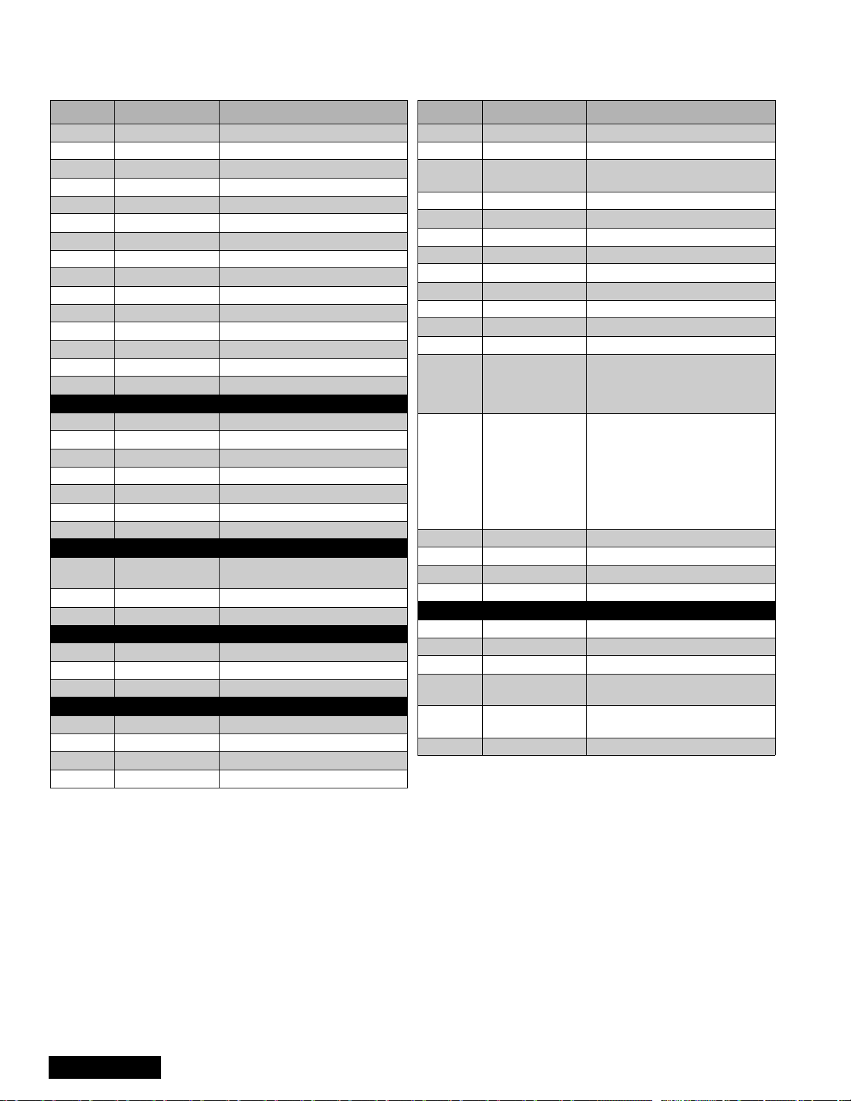
REPLACEMENT PARTS LIST
Model:CT-24SX11E, CT-24SX11UE, CT-24S X11CE
Important Safety Notice: Components printed in BOLD TYPE have special characteristics important for safety. When replacing
any of these components use only manufacturer’s specified parts.
REF NO. PART NO. DESCRIPTION
R6510 ERJ6GEYJ471V RES,M 470-J-1/10W
R6512 ERJ6GEYJ471V RES,M 470-J-1/10W
R6513 ERJ6GEYJ122V RES,M 1.2K-J-1/10W
R6514 ERJ6GEYJ123V RES,M 12K-J-1/10W
R6516 ERJ6GEYJ103V RES,M 10K-J-1/10W
R6517 ERJ6GEYJ471V RES,M 470-J-1/10W
R6520 ERJ6GEYJ102V RES,M 1K-J-1/10W
R6522 ERJ6GEYJ471V RES,M 470-J-1/10W
R6524 ERJ6GEYJ471V RES,M 470-J-1/10W
R6538 ERJ6GEYJ821V RES,M 820-J-1/10W
R6548 ERJ6GEYJ471V RES,M 470-J-1/10W
R6565 ERJ6GEYJ102V RES,M 1K-J-1/10W
R6566 ERJ6GEYJ681V RES,M 680-J-1/10W
R6567 ERJ6GEYJ102V RES,M 1K-J-1/10W
R6568 ERJ6GEYJ102V RES,M 1K-J-1/10W
SWITCHES
S001 EVQPC105K SWITCH
S002 EVQPC105K SWITCH
S003 EVQPC105K SWITCH
S004 EVQPC105K SWITCH
S005 EVQPC105K SWITCH
S006 EVQPC105K SWITCH
S007 EVQPC105K SWITCH
TRANSFORMERS
T501 ETH19Y70AY
T551 KFT4AA390F TRANSFORMER, FLYBACK
T801 ETS39AG375NC TRANSFORMER
CRISTALS/FILTERS
X001 TSSA092 CRYSTAL OSCILLATOR
X501 TSS2AA001 CRYSTAL, 3.58MHZ
X601 TAFCSB503F30 CRYSTAL
TNR001 ENG36604G TUNER
M001 TSX2AA0111-1 A/C LINE CORD
M002 A60LUQ085X CRT 25”
M003 TJSC01200 CRT SOCKET
TRANSFORMER, HORIZONTAL
DRIVER
OTHERS
REF NO. PART NO. DESCRIPTION
DY KDY 4QHA31F YOKE, DEFLECTION
DEG TSP2AA014 COIL, DEGAUSS ING 27”
M004 0FMK014ZZ
M005 TXF3A011DD ASSY., DAG GND
M006 TAS2AA0023 SPEA KER 8-OHM
M007 TBM2A30843 B ADGE, PANASONIC
M008 TBX2AA0151G BUTTON, 7-KEY
M009 TEK6940 DOOR CATCH
M010 TKP2AA0613S CONTROL DOOR
M011 TKX2AA0131 IR GUIDE
M012 TMW2A97121 STRAIN RELIEF: AC LINE CORD
M013 TXFEA0041DBS SPEAKER BRACKETS
M014 TXFKY40ESER
M015 TXFKU30ESER
JK3001 TJB2AA0221 TERMINAL, A/V 8P
JK3002 TJB2AA01 71 TERMINAL, S-VHS
JK3003 TJB2AA0371 TERMINAL, FRONT A/V
JK3005 TJB2AA02 11-1 TERMINAL, A/V 2P
M016 EUR511502 REMOTE CONTROL
M017 UR51EC975A BATTERY COVER, REMOTE CON
M018 TQB2AA7058 REMOTE GUIDE
M019 TQB2AA0377
M020 TQB2AA0409
M021 TQB2AA7078-1 V-CHIP NA8
CONVERGENCE CORRECTOR
STRIP
ASSY, CABINET FRONT
(2)Rubber sheet,(1)Badge panasonic
(1) IR Guide,(1)Cabinet,
(1)Felt,Rl 8mm x 46M
ASSY, CA BI NET BA CK
(2)Rubber sheet,
(1)Overlay modelnameplate,
(1)Name platemodel,
(1)cover,cabinetback,(1)felt ,
(1)Instr.Sheet labels, (1)Label,X-RAY
warning frn. (2)Label,XRAYWarning
(1)Label,BBE patent
ACCSESORIES
MANUAL, OWNERS
CT-24SX11E/UE
MANUAL, OWNERS
CT-24SX11CE
PARTS LIST
Parts List
- 26 -
201-01
Page 27
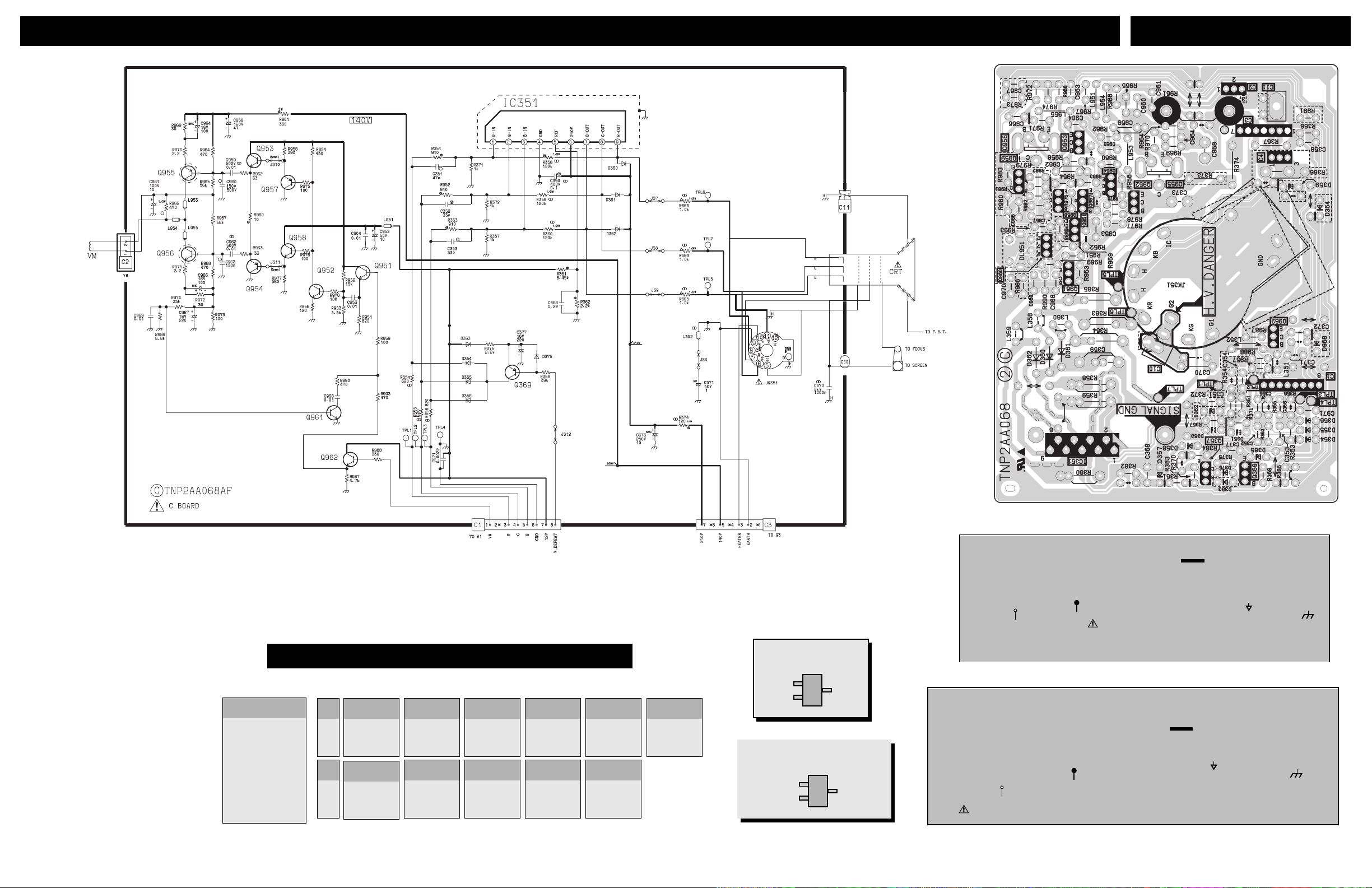
C- Board Schematic, Layout & Voltages - Diagrama Eléctrico, Diagrama Impreso y Voltajes Tarjeta-C
ALL MODELS
IC351
1
. . . . . .1.75
2
. . . . . .1.75
3
. . . . . .1.76
4
. . . . . .0.00
5
. . . . . .1.85
6
. . . .218.39
7
. . . .141.10
8
. . . .142.90
9
. . . .144.90
C-Board V oltages - Voltajes Placa-C
Q369
B
C
E
6.90
2.11
8.39
Q956
B
C
E
1.00
73.80
0.00
Q951
2.48
8.93
1.85
Q957
7.20
0.00
7.84
Q952
1.13
7.20
0.49
Q958
7.19
8.93
6.51
Q953
7.84
8.93
7.20
Q961
0.00
0.00
0.00
Q954
6.51
0.00
7.15
Q962
3.10
8.94
2.49
Q955
141.90
73.70
142.40
- 27 -
CHIP TRANSISTOR
LEAD DESIGNATION
B
E
IDENTIFICACIÓN DE TERMINALES
PARA TRANSISTORE S EN
B
E
C
CHIP
C
Schematic Notes
1. Resistors are carbon 1/4W unless noted
otherwise.
2. Ca pacitors are ceramic 50V un less noted
otherwise.
3. Coil valu e n otes is inductance in µH.
4. Test point indicated by ; Test point but
no pin .
5. Co mponents in dicated w ith are criti cal
parts and replacement should be made
with manufacture specified replacement
parts only.
Notas de los Diagramas
1. Las Res istencias son de Carbón de 1/4W, a
menos que se indique otra característica.
2. Los Capacitores son de Cerámica para 50V, a
menos que se indique otra característica.
3. El valor indicado de las Bobinas es la
inductancia expresada en µH.
4. Los p untos de prueb a en la term inal de algún
componente son indicados por Los puntos
de prueba fuera de los componentes se
indican con .
5. Los componentes señalados con el símbolo
son considerados compon entes críticos y
6. (BOLD LINE) indicates the
route of B+ supply.
7. The schematic diagrams are current at
the time of printing an d are subject to
change without notice.
8. Ground symbol indicates HOT
GROUND CONNECTION;
indicates COLD GROUND.
NOTE: All other component symbols are
used for engineering design
purposes.
deben ser reemplazado s sólo con las partes
especificadas por el fabricante.
6. (LINEA GRUESA) indica las líneas de
alimentación de los Voltajes B+.
7. Los diagramas eléctricos están sujetos a
cambio sin previo aviso.
8. El símbolo indica que es una conexión a
Tierra Caliente y el símbolo indica
conexión a Tierra F ría.
NOTA: Los demas símbolos de componentes
incluidos son usados con fines de
diseño.
Page 28
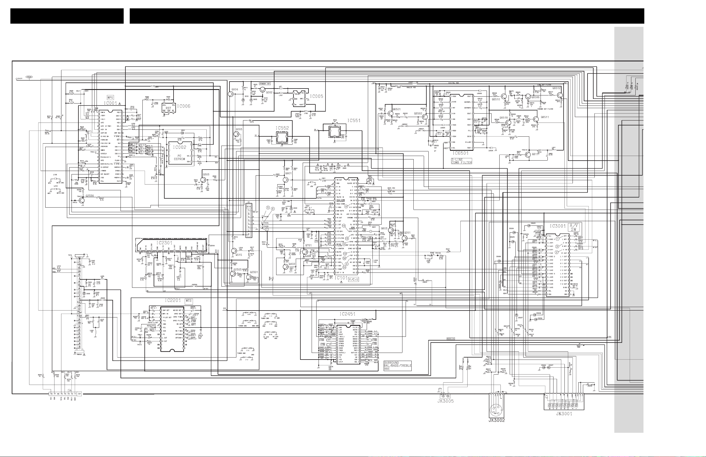
ALL MODELS
A-Board Schematic, Left Portion - Diagrama Eléctrico de la Tarjeta-A, Sección Izquierda
- 28 -
Page 29
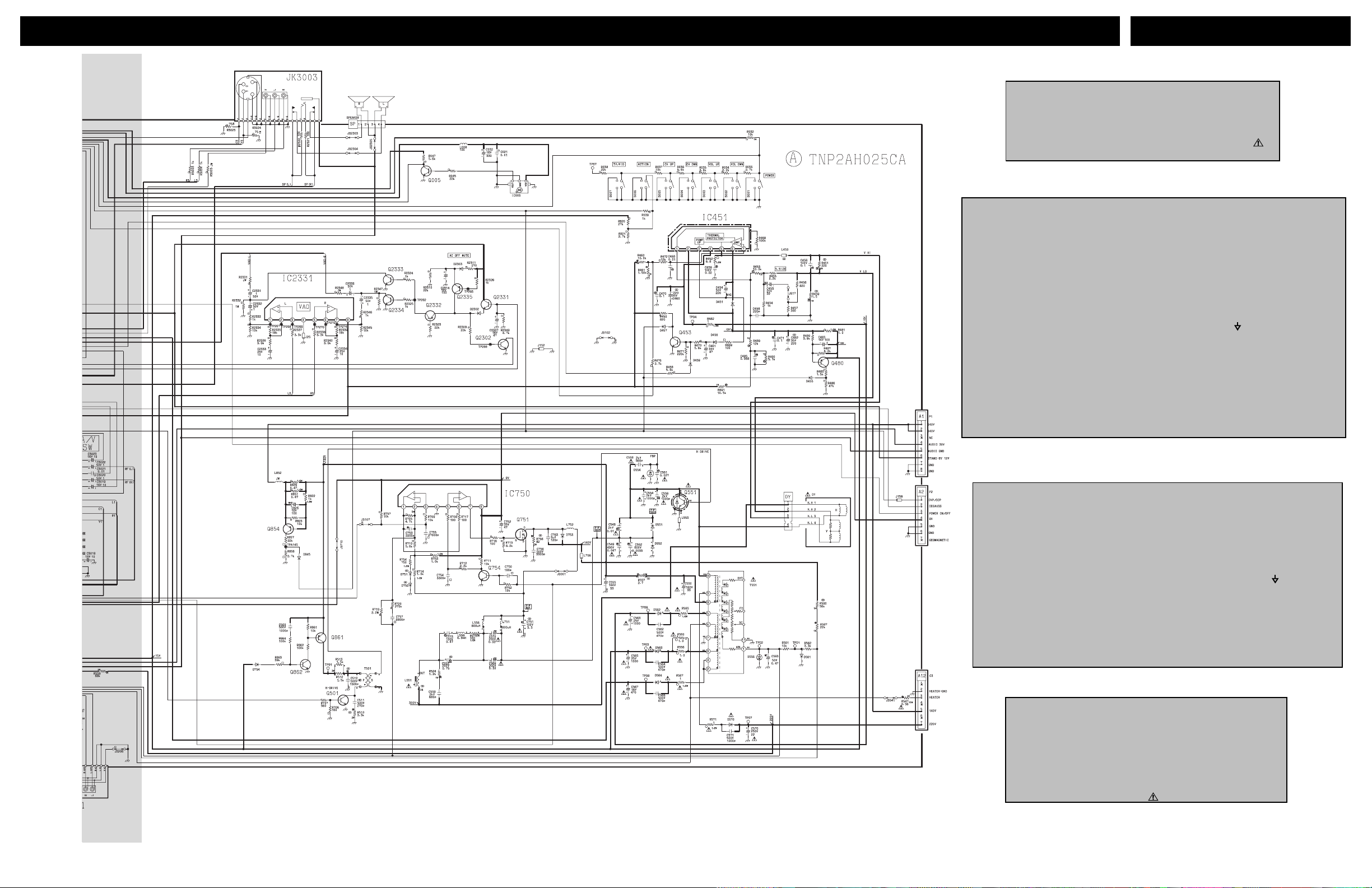
A-Board Schematic, Right Portion - Diagrama Eléctrico de la Tarjeta-A, Sección Derecha
ALL MODELS
IMPORTANT SAFETY NOTICE
THIS SCHEMATIC DIAGRAM INCORPORATES SPECIAL FEATURES
THAT ARE IMPORTANT FOR PROTECTION FROM X-RADIATION, FIRE
AND ELECTRICAL SHOCK HAZARDS. WHEN SERVICING IT IS
ESSENTIAL THAT ONLY MANUFACTURERS SPECIFIED PARTS BE
USED FOR THE CRITICAL COMPONENTS DESIGNATED WITH A IN
THE SCHEMATIC.
1. Medición de voltaje:
- El voltaje de entrada al Receptor
es de 120V de Corriente Alterna.
Un generador de patrones con
formato NTSC se conecta a la
entrada de la antena. (Patrón de
Barras de Colores con 100 IREs
para el Blanco y 7.5 IREs para el
Negro.)
- Los ajustes de los Menus Picture y
Audio se normalizan.
En el Menú Set-Up, en la opción
ANTENA, se selecciona el modo de
CABLE.
El nivel de Volumen se minimiza.
De los modos TV y Video,
seleccionar el modo TV.
Seleccionar modo Estereo del
Audio.
Medición de Voltajes
- Las mediciones de los voltajes
son nominales y pueden variar
hasta 10% en componentes en
funcionamiento. Las lecturas
de los voltajes pueden variar
por la potencia de la señal y el
contenido de la imagen.
- Las fuentes de voltajes son
nominales.
2. El símbolo indica el tipo de tierra
que se utiliza en la conexión del
medidor.
PRECAUCION: Si no se utiliza la
conexión a la tierra adecuada, se
obtendrán mediciones equivocadas
y podría dañar el equipo de
medición.
Voltage Measurements
1. Voltage measurement:
- AC input to the Receiver is 120V.
NTSC (HD, 1125i & 525P when
applicable) signal generator is
connected to the antenna of the
Receiver. (Color bar pattern of
100 IRE white and 7.5 IRE black.)
- All Picture and Audio adjust men ts
are set to Normalize.
TV ANT/CABLE - (Set-Up Menu)
in TV/ANT Mode
Vol ume - Mi n.
TV/Video SW - TV position
Audio Mode - Stereo
NOTA DE SEGURIDAD
LOS DIAGRAMAS ELÉCTRICOS INCLUYEN CA RACTERÍSTICAS
ESPECIALES MUY IMPORTANTES PARA LA PROTECCIÓN
CONTRA RAYOS-X, QUEMADURAS Y DESCARGAS
ELÉCTRICAS. CUANDO SE DE SERVICIO ES IMPORTANTE
USAR PARA REEMPLAZO DE COMPONENTES CRITICOS,
SOLO PARTES ESPECIFICADAS POR EL FABRICANTES. LOS
COMPONENTES CRITICOS ESTAN SEÑALADOS EN LOS
DIAGRAMAS POR EL SIMBOLO
- Voltage readings are nominal
and may vary ±10% on active
devices. Some voltage
reading will vary with signal
strength and picture content.
- Supply voltages are nominal.
2. Ground symbol indicates
ground lead connection of meter.
Incorrect ground connection will
result in erroneous readings.
CAUTION: Incorrect ground
connection of the test equipment
will result in erroneous readings.
.
- 29 -
Page 30
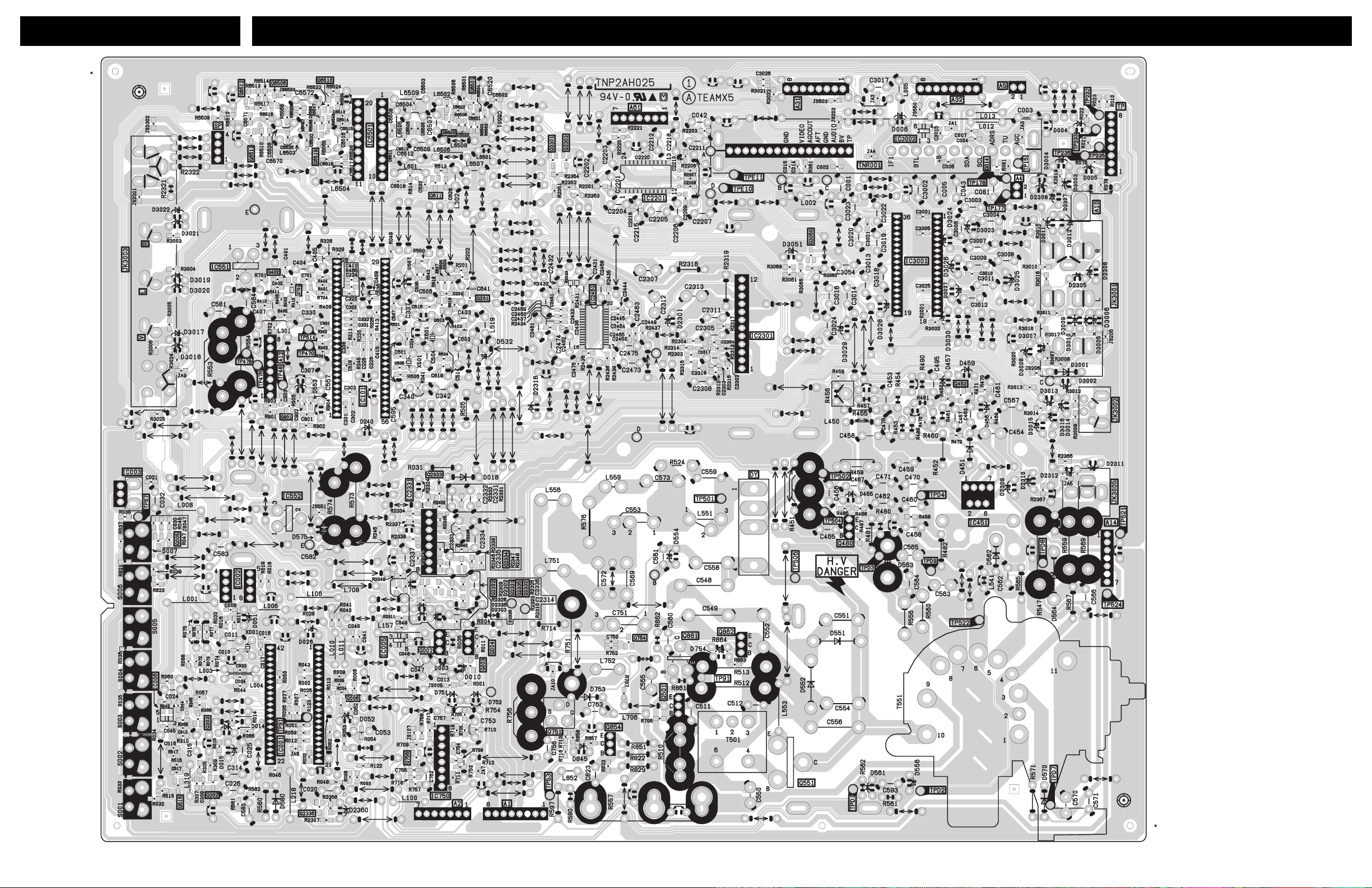
ALL MODELS
A-Board Layout - Diagrama Impreso de la Tarjeta-A
A-BOARD LAYOUT
- 30 -
Page 31
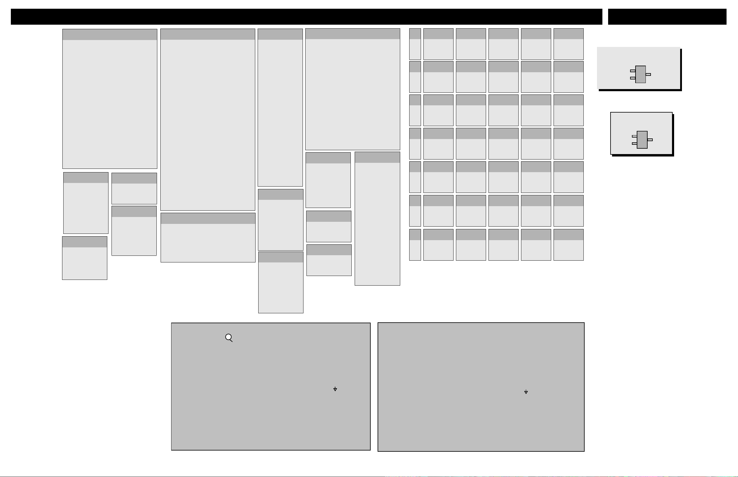
A-Board Voltages - Voltajes Tarjeta- A
ALL MODELS
1
. . . . . .0.00
2
. . . . . .4.75
3
. . . . . .4.80
4
. . . . . .1.73
5
. . . . . .0.77
6
. . . . . .3.26
7
. . . . . .1.71
8
. . . . . .3.26
9
. . . . . .0.00
10
. . . . . .1.64
11
. . . . . .0.00
12
. . . . . .3.26
13
. . . . . .1.64
14
. . . . . .0.00
15
. . . . . .0.00
16
. . . . . .0.00
17
. . . . . .0.00
18
. . . . . .3.14
19
. . . . . .0.62
20
. . . . . .3.28
21
. . . . . .1.51
IC002
1
. . . . . 0.00
2
. . . . . 0.00
3
. . . . . 0.00
4
. . . . . 0.00
5
. . . . . 5.00
6
. . . . . 0.00
7
. . . . . 3.84
8
. . . . . 3.88
IC006
1
. . . . . .0.00
2
. . . . . .0.00
3
. . . . . .0.00
4
. . . . . .3.28
5
. . . . . .3.28
IC001
22
. . . . . .2.07
23
. . . . . .2.41
24
. . . . . .1.61
25
. . . . . .1.55
26
. . . . . .2.40
27
. . . . . .2.76
28
. . . . . .0.00
29
. . . . . .0.00
30
. . . . . .0.00
31
. . . . . .0.00
32
. . . . . .0.00
33
. . . . . .0.00
34
. . . . . .3.28
35
. . . . . .3.50
36
. . . . . .3.24
37
. . . . . .3.91
38
. . . . . .3.83
39
. . . . . .3.28
40
. . . . . .1.57
41
. . . . . .1.54
42
. . . . . .0.00
IC003
1
. . . . . 2.77
2
. . . . . 0.00
3
. . . . . 4.99
IC005
1
. . . . . 4.99
2
. . . . . 0.00
3
. . . . . 1.29
4
. . . . . 3.28
5
. . . . . 0.00
6
. . . . . 4.98
1
. . . . . 4.11
2
. . . . . 0.00
3
. . . . . 3.36
4
. . . . . 3.35
5
. . . . . 3.34
6
. . . . . 0.00
7
. . . . . 6.03
8
. . . . . 5.05
9
. . . . . 5.16
10
. . . . . 0.00
11
. . . . . 5.63
12
. . . . . 4.51
13
. . . . . 2.76
14
. . . . . 2.81
15
. . . . . 2.88
16
. . . . . 8.71
17
. . . . . 5.26
18
. . . . . 5.25
19
. . . . . 2.24
20
. . . . . 2.69
21
. . . . . 2.96
22
. . . . . 3.03
23
. . . . . 0.68
24
. . . . . 0.66
25
. . . . . 5.15
26
. . . . . 2.05
27
. . . . . 4.30
28
. . . . . 4.98
1
. . . . . 0.00
2
. . . . . 0.00
3
. . . . 29.59
4
. . . . . 0.00
5
. . . . . 0.00
6
. . . . . 0.00
IC101
29
30
31
32
33
34
35
36
37
38
39
40
41
42
43
44
45
46
47
48
49
50
51
52
53
54
55
56
IC2301
10
11
12
. . . . . .3.86
. . . . . .3.81
. . . . . .0.00
. . . . . .0.00
. . . . . .4.85
. . . . . .1.19
. . . . . .1.87
. . . . . .0.00
. . . . . .9.15
. . . . . .3.14
. . . . . .6.34
. . . . . .7.68
. . . . . .6.00
. . . . . .4.92
. . . . . .1.11
. . . . . .0.00
. . . . . .1.76
. . . . . .1.42
. . . . . .2.25
. . . . . .2.27
. . . . . .3.90
. . . . . .3.37
. . . . . .4.93
. . . . . .2.97
. . . . . .3.39
. . . . . .3.77
. . . . . .3.10
. . . . . .3.21
7
. . . . 14.85
8
. . . . . 0.67
9
. . . . . 0.00
. . . . 30.84
. . . . 11.83
. . . . 14.87
IC2201
1
. . . . . 0.00
2
. . . . . 0.00
3
. . . . . 0.00
4
. . . . . 2.22
5
. . . . . 2.18
6
. . . . . 0.34
7
. . . . . 4.92
8
. . . . . 2.24
9
. . . . . 2.42
10
. . . . . 0.43
11
. . . . . 2.24
12
. . . . . 3.09
13
. . . . . 3.30
14
. . . . . 2.75
15
. . . . . 3.33
16
. . . . . 3.43
17
. . . . . 0.00
18
. . . . . 3.62
19
. . . . . 3.83
20
. . . . . 0.00
21
. . . . . 2.20
22
. . . . . 2.19
23
. . . . . 0.00
24
. . . . . 0.00
IC2331
1
. . . . . 4.46
2
. . . . . 4.46
3
. . . . . 4.46
4
. . . . . 0.00
5
. . . . . 4.46
6
. . . . . 4.46
7
. . . . . 4.46
8
. . . . . 8.93
IC750
1
. . . . . 2.33
2
. . . . . 3.58
3
. . . . . 3.57
4
. . . . . 0.00
5
. . . . . 4.55
6
. . . . . 2.33
7
. . . . . 7.37
8
. . . . . 8.93
1
. . . . . 8.91
2
. . . . . 3.59
3
. . . . . 4.58
4
. . . . . 4.59
5
. . . . . 4.58
6
. . . . . 3.57
7
. . . . . 3.60
8
. . . . . 4.58
9
. . . . . 4.59
10
. . . . . 4.58
11
. . . . . 3.60
12
. . . . . 4.58
13
. . . . . 4.59
14
. . . . . 4.58
15
. . . . . 4.58
16
. . . . . 3.59
17
. . . . . 4.83
18
. . . . . 4.76
IC451
1
. . . . . 1.33
2
. . . . 16.52
3
. . . .-13.99
4
. . . .-15.77
5
. . . . . 0.25
6
. . . . 16.52
7
. . . . . 1.32
IC552
1
. . . . . 8.89
2
. . . . . 0.00
3
. . . . . 4.94
IC551
1
. . . . .16.81
2
. . . . . .0.00
3
. . . . . .8.94
IC3001
19
20
21
22
23
24
25
26
27
28
29
30
31
32
33
34
35
36
10
11
12
13
14
15
16
17
18
19
20
. . . . . 0.00
. . . . . 0.00
. . . . . 4.08
. . . . . 3.26
. . . . . 3.91
. . . . . 3.93
. . . . . 3.92
. . . . . 3.32
. . . . . 3.26
. . . . . 3.91
. . . . . 3.93
. . . . . 3.92
. . . . . 3.77
. . . . . 3.94
. . . . . 4.58
. . . . . 4.59
. . . . . 4.58
. . . . . 3.99
IC6501
1
. . . . . 4.92
2
. . . . . 1.36
3
. . . . . 3.12
4
. . . . . 2.39
5
. . . . . 1.82
6
. . . . . 4.92
7
. . . . . 0.00
8
. . . . . 4.91
9
. . . . . 4.75
. . . . . 4.83
. . . . . 0.00
. . . . . 0.00
. . . . . 2.48
. . . . . 1.97
. . . . . 4.97
. . . . . 0.00
. . . . . 2.46
. . . . . 3.11
. . . . . 1.82
. . . . . 2.33
Q002
B
C
E
5.67
8.81
5.00
Q2301
B
C
E
0.69
0.00
0.00
Q2333
B
C
E
0.00
0.00
0.00
Q402
B
C
E
0.68
3.49
0.00
Q551
B
C
E
0.00
13.3
0.00
Q6506
B
C
E
0.00
1.69
0.00
Q701
B
C
E
0.65
3.04
0.00
Q003
0.00
9.81
0.00
Q2302
0.00
0.13
0.00
Q2334
0.00
0.00
0.00
Q453
0.72
0.00
0.00
Q603
1.06
4.92
0.99
Q6510
2.33
4.92
1.69
Q751
7.28
11.81
0.00
Q004
9.89
14.50
9.23
Q2303
0.00
11.83
0.00
Q2335
14.5
0.00
13.42
Q480
16.63
0.00
16.86
Q611
0.00
0.00
0.69
Q6511
2.30
4.89
1.70
Q754
0.00
4.49
0.00
Q005
0.64
0.00
0.00
Q2331
0.00
14.15
0.00
Q2336
0.62
0.00
0.00
Q501
0.30
106.50
0.00
Q6501
2.92
4.92
2.26
Q6512
1.70
4.90
1.00
Q854
142.90
0.00
143.40
Q201
3.25
4.92
2.58
Q2332
0.00
0.00
0.00
Q303
3.73
4.94
3.10
Q515
0.00
2.76
0.00
Q6502
1.13
0.00
1.81
Q6519
2.50
2.33
1.80
Q901
3.45
3.10
2.77
IDENTIFICACIÓN DE TERMINALES
PARA TRANSISTORE S EN
B
E
CHIP TRANSISTOR
LEAD DESIGNATION
B
E
CHIP
C
C
Nota:
La medición de los voltajes se
hizo con un Voltímetro Digital.
Note:
Obtained voltages with a digital
multimeter.
Medición de Formas de Onda
1. Un símbolo como indica el punto
para medir una señal. (La medic ión
puede hacerse en el punto con
mayor accesibilidad, siempre que
sea común al indicado.)
2. Se midieron utilizando un
generador con formato NTSC
conectado a la terminal de la
antena. (Patrón de 8 Barras de
Colores EAI, formato NTSC de 100
IREs para el Blanco y 7.5 IREs
para el Negro.)
3. Los ajustes de usuario de los
Menus PICTURE y AUDIO se
normalizaron. Posteriormente el
nivel de volumen se ajusta al
mínimo.
3
4. Las formas de onda de Video y
Color fueron tomadas con un
osciloscopio de banda alta y con un
punta de prueba de baja
capacitancia (10 a 1). La forma y
amplitud de las ondas puede variar
según el tipo de osciloscopio que
se utilice y sus características.
5. El símbolo de tierra que apar ece
junto al número de la forma de
onda, indica que se utiliza conexión
a Tierra Caliente en el extremo
negativo de la punta de prueba.
PRECAUCION: Si no se utiliza la
conexión a la tierra adecuada, se
obtendrán mediciones equivocadas
y podría dañar el equipo de
medición.
- 31 -
1. Medición de voltaje:
- El voltaje de entrada al Receptor
es de 120V de Corriente Alterna.
Un generador de patrones con
formato NTSC se conecta a la
entrada de la antena. (Patrón de
Barras de Colores con 100 IREs
para el Blanco y 7.5 IREs para el
Negro.)
- Los ajustes de los Menus Picture y
Audio se normalizan.
En el Menú Set-Up, en la opción
ANTENA, se selecciona el modo de
CABLE.
El nivel de Volumen se minimiza.
De los modos TV y Video,
seleccionar el modo TV.
Seleccionar modo Estereo del
Audio.
Medición de Voltajes
- Las mediciones de los voltajes
son nominales y pueden variar
hasta 10% en componentes en
funcionamiento. Las lecturas
de los voltajes pueden variar
por la potencia de la señal y el
contenido de la imagen.
- Las fuentes de voltajes son
nominales.
2. El símbolo indica el tipo de tierra
que se utiliza en la conexión del
medidor.
PRECAUCION: Si no se utiliza la
conexión a la tierra adecuada, se
obtendrán mediciones equivocadas
y podría dañar el equipo de
medición.
Page 32
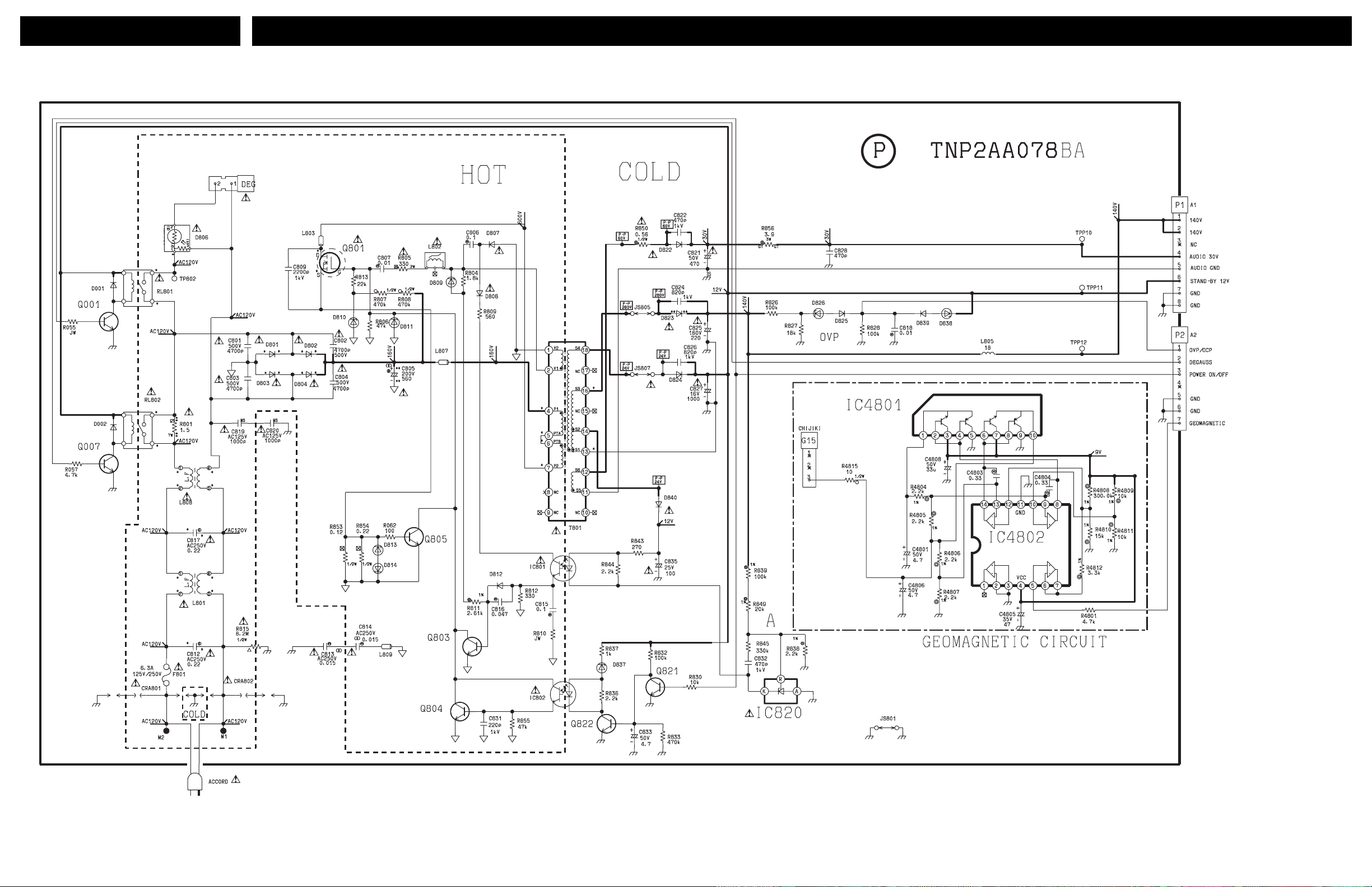
ALL MODELS
P-Board Schematic, Layout & Voltages - Diagrama Impreso, Eléctrico y Voltajes Tarjeta-P
L
V
- 32 -
Page 33
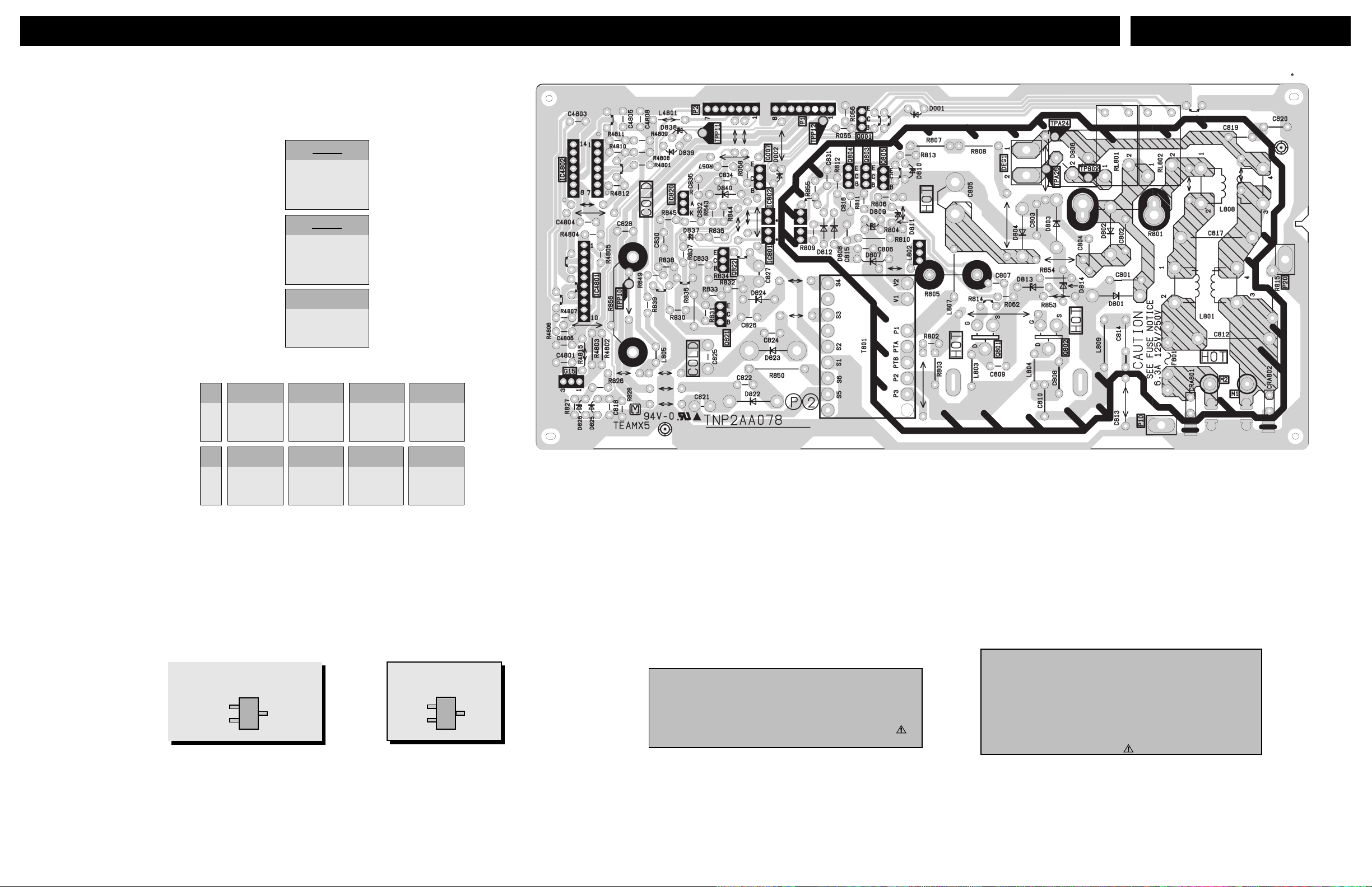
IC801
1
. . . . 14.09
2
. . . . 15.76
3
. . . . . 0.16
4
. . . . 13.02
IC802
1
. . . . .11.00
2
. . . . . 3.45
3
. . . . . 0.00
4
. . . . .11.00
IC820
1
. . . . 13.02
2
. . . . . 0.00
3
. . . . . 2.44
P- Board Layout & Volt ages - Cir cuito Impreso y Voltajes Tarjeta-P
ALL MODELS
Q001
B
C
E
0.00
0.00
0.00
Q821
B
C
E
IDENTIFICACIÓN DE TERMINALES
PARA TRANSISTORE S EN
0.56
0.00
0.00
B
E
Q007
Q822
11.00
CHIP
C
0.69
0.36
0.00
0.00
0.00
Q801
0.10
-30.50
3.43
Q804
0.00
3.45
0.00
Q803
0.00
3.40
0.00
Q805
0.00
3.43
0.00
CHIP TRANSISTOR
LEAD DESIGNATION
B
E
C
Nota:
La medición de los voltajes se
hizo con un Voltímetro Digital.
IMPORTANT SAFETY NOTICE
THIS SCHEMATIC DIAGRAM INCORPORATES SPECIAL FEATURES
THAT ARE IMPORTANT FOR PROTECTION FROM X-RADIATION, FIRE
AND ELECTRICAL SHOCK HAZARDS. WHEN SERVICING IT IS
ESSENTIAL THAT ONLY MANUFACTURERS SPECIFIED PARTS BE
USED FOR THE CRITICAL COMPONENTS DESIGNATED WITH A IN
THE SCHEMATIC.
Note:
Obtained voltages with a digital
multimeter.
NOTA DE SEGURIDAD
LOS DIAGRAMAS ELÉCTRICOS INCLUYEN CA RACTERÍSTICAS
ESPECIALES MUY IMPORTANTES PARA LA PROTECCIÓN
CONTRA RAYOS-X, QUEMADURAS Y DESCARGAS
ELÉCTRICAS. CUANDO SE DE SERVICIO ES IMPORTANTE
USAR PARA REEMPLAZO DE COMPONENTES CRITICOS,
SOLO PARTES ESPECIFICADAS POR EL FABRICANTES. LOS
COMPONENTES CRITICOS ESTAN SEÑALADOS EN LOS
DIAGRAMAS POR EL SIMBOLO
.
- 33 -
Page 34
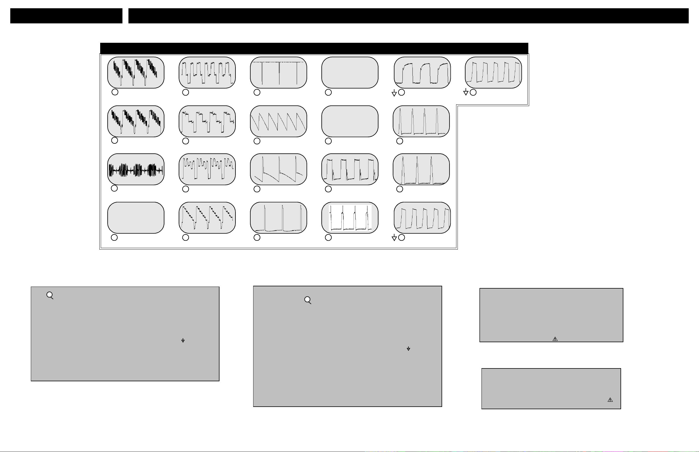
ALL MODELS
A-Board Waveforms - Formas de Onda Tarjeta A
Waveforms - A-Board
N/A
1.0-1.1V p-p [20µs]
1
IC3001 PIN 36 (VIDEO)
1.1-1.3V p-p [20µs]
2
IC3001 PIN 32 (Y IN)
0.8 p-p [20µs]
3
IC3001 PIN 34 (C IN)
3.58MHz X’tal
IC101 PIN 49
4
3.58VCO
OSC
3.9-5.4V p-p [20µs]
5
6
7
8
(R OUT)
TP47R
3.8-5.0V p-p [20µs]
(G OUT)
TP47G
3.8-5.1V p-p [20µs]
(B OUT)
TP47B
1.0-1.2V p-p [20µs]
IC101 PIN 38 (SYNC)
4.1-4.2V p-p [5ms]
9 13
IC101 PIN 33 (VERT OUT)
1.2-1.3V p-p [5ms]
10
IC101 PIN 25 (DRIVE)
53.6-56.3V p-p [5ms]
11
IC451 PIN 2 (VERT OUT)
28.4-30.0V p-p [5ms]
12
IC451 PIN 3
503KHz X’tal
IC101 PIN 41
14
15
16
IC101 PIN 34 (H SYNC)
H OSC
OSC
5.9-6.1V p-p [20µs]
IC101 PIN 35 (H OUT)
7.7-7.9V p-p [20µs]
178.0-180.0V p-p [20µs]
17
Q501 Collector (H DRIVE)
268.0-272.0V p-p [20µs]
18
19
T551 PIN 1
27.2-27.6V p-p [20µs]
T551 PIN 6
344.0-348.0V p-p [5µs]
20
IC803 PIN 2
344.0-348.0V p-p [5µs]
21
Q802 Collector
3
Waveform Measurements
1. indicates waveform measurement.
(Measurement can be taken at the
best accessible location in common
to the indicated point.)
2. Taken with an NTSC signal
generator connected to the antenna
terminal. (NTSC color bar pattern of
8 bars of EIA colors, 100 IRE white
and 7.5 IRE black.)
3. Customer Controls (Picture/Audio
Menu) are set to Normalize. Volume
is set to “MIN”.
4. All video and color waveforms are
taken with a wideband scope and
a probe with low capacitance (10
to 1). Shape and peak altitudes
may vary depending on the type
of Oscilloscope used and its
settings.
5. Ground symbol shown on
waveform number indicates (Hot)
ground lead connection of the
Oscilloscope.
CAUTION: Incorrect ground
connection of the test equipm ent will
result in errone ous re ad in gs .
Medición de Formas de Onda
1. Un símbolo como indica el punto
para medir una señal. (La medic ión
puede hacerse en el punto con
mayor accesibilidad, siempre que
sea común al indicado.)
2. Se midieron utilizando un
generador con formato NTSC
conectado a la terminal de la
antena. (Patrón de 8 Barras de
Colores EAI, formato NTSC de 100
IREs para el Blanco y 7.5 IREs
para el Negro.)
3. Los ajustes de usuario de los
Menus PICTURE y AUDIO se
normalizaron. Posteriormente el
nivel de volumen se ajusta al
mínimo.
3
4. Las formas de onda de Video y
Color fueron tomadas con un
osciloscopio de banda alta y con un
punta de prueba de baja
capacitancia (10 a 1). La forma y
amplitud de las ondas puede variar
según el tipo de osciloscopio que
se utilice y sus características.
5. El símbolo de tierra que apar ece
junto al número de la forma de
onda, indica que se utiliza conexión
a Tierra Caliente en el extremo
negativo de la punta de prueba.
PRECAUCION: Si no se utiliza la
conexión a la tierra adecuada, se
obtendrán mediciones equivocadas
y podría dañar el equipo de
medición.
- 34 -
NOTA DE SEGURIDAD
LOS DIAGRAMAS ELÉCTRICOS INCLUYEN CA RACTERÍSTICAS
ESPECIALES MUY IMPORTANTES PARA LA PROTECCIÓN
CONTRA RAYOS-X, QUEMADURAS Y DESCARGAS
ELÉCTRICAS. CUANDO SE DE SERVICIO ES IMPORTANTE
USAR PARA REEMPLAZO DE COMPONENTES CRITICOS,
SOLO PARTES ESPECIFICADAS POR EL FABRICANTES. LOS
COMPONENTES CRITICOS ESTAN SEÑALADOS EN LOS
DIAGRAMAS POR EL SIMBOLO
IMPORTANT SAFETY NOTICE
THIS SCHEMATIC DIAGRAM INCORPORATES SPECIAL FEATURES
THAT ARE IMPORTANT FOR PROTECTION FROM X-RADIATION, FIRE
AND ELECTRICAL SHOCK HAZARDS. WHEN SERVICING IT IS
ESSENTIAL THAT ONLY MANUFACTURERS SPECIFIED PARTS BE
USED FOR THE CRITICAL COMPONENTS DESIGNATED WITH A IN
THE SCHEMATIC.
.
Page 35
PARTS LIST ABBREVIATIONS GUIDE
RESISTOR
TYPE TOLERANCE
CCarbonF± 1%
FFuseJ± 5%
M Metal Oxide K± 10%
S Solid M± 20%
WWire WoundG± 2%
RES, C 270-J-1/4
CAPACITOR
TYPE TOLERANCE
C Ceramic C ± 0.25pF
E Electrolytic D ± 0.5pF
P Polyester F± 1pF
S Styrol J± 5%
T Tantalum K± 10%
L± 15%
M± 20%
P +10% -0%
Z +80% -20%
CAP, P .068UF-K-50V
- 35 -
Page 36

®
- 32 -
Printed in USA
K01072223CM0731
 Loading...