

Page 1
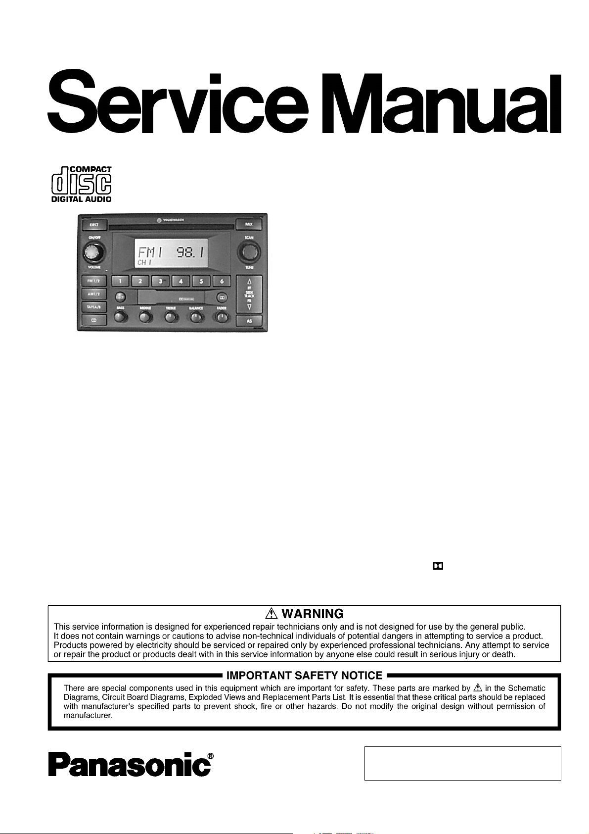
ORDER No. AED0106025
AUTOMOTIVE ELECTRONICS
V.W.
CQ-JV1060L
AM/FM MPX ELECTRONIC TUNING
RADIO with Stereo Cassette Tape
Player and CD Player
V.W. PART No. : 3B7 035 180
VEHICLE : PASSAT, GOLF, JETTA
DESTINATION : North America
PRODUCED AFTER : Aug., 2001
I0
Specification*
General
Power Supply DC 12V (11V - 16V),
Test Voltage 14.4V
Negative Ground
Current Consumption Less than 2.5A (0.5W×4ch)
Power Output 45W×4ch (at 0.5W)
Speaker Impedance 4Ω
AM Radio
Frequency Range 530 - 1,710kHz
Usable Sensitivity 23dB/µV (S/N 20dB)
FM Stereo Radio
Frequency Range 87.9 - 107.9MHz
Usable Sensitivity 4dB/µV (S/N 26dB)
CD Player
Decoding 16bit (Linear)
Signal to Noise Ratio More than 70dB (IHF-A)
Channel Separation More than 50dB (IHF-A)
Dimensions** 189(W)×111(H)×170(D)mm
Weight** 2.6kg
* Specifications and the design are subject to possible modification
without notice due to improvements.
** Dimensions and Weight shown are approximate.
Doldy noise reduction manufactured under license from Dolby
Laboratories Licensing Corporation.
“Dolby” and the double-D symbol
Laboratories Licensing Corporation.
are trade marks of Dolby
© 2001 Matsushita Communication Industrial Co.,
Ltd. All rights reserved. Unauthorized copying and
distribution is a violation of law.
Page 2
V.W. / CQ-JV1060L
CONTENTS
Page Page
1 FEATUERS 2
2 LASER PRODUCTS
3 REAR VIEW
4 FRONT VIEW AND FUNCTIONS
5 WIRING CONNECTION
6 BLOCK DIAGRAM
7 TERMINALS DESCRIPTION
8 PACKAGE AND IC BLOCK DIAGRAM
9 REPLACEMENT PARTS LIST 13
2
10 EXPLODED VIEW (Unit)
11 CD PLAYER PARTS
2
3
12 EXPLODED VIEW (CD Deck)
4
13 TAPE PLAYER PARTS
14 EXPLODED VIEW (Tape Deck)
5
8
15 WIRING DIAGRAM
10
16 SCHEMATIC DIAGRAM
21
22
23
24
25
26
35
1 FEATUERS
±
PLL (Phase Locked Loop) synthesized tuning.
±
12-FM, 12-AM presets with preset scan
±
Dolby noise reduction.
±
NCD-8 CD player.
±
CD Changer control.
2 LASER PRODUCTS
3 REAR VIEW
2
Page 3
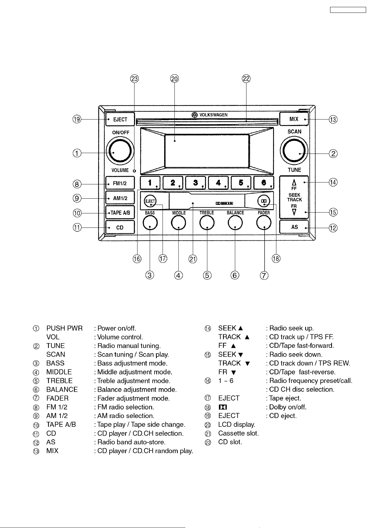
4 FRONT VIEW AND FUNCTIONS
V.W. / CQ-JV1060L
3
Page 4
V.W. / CQ-JV1060L
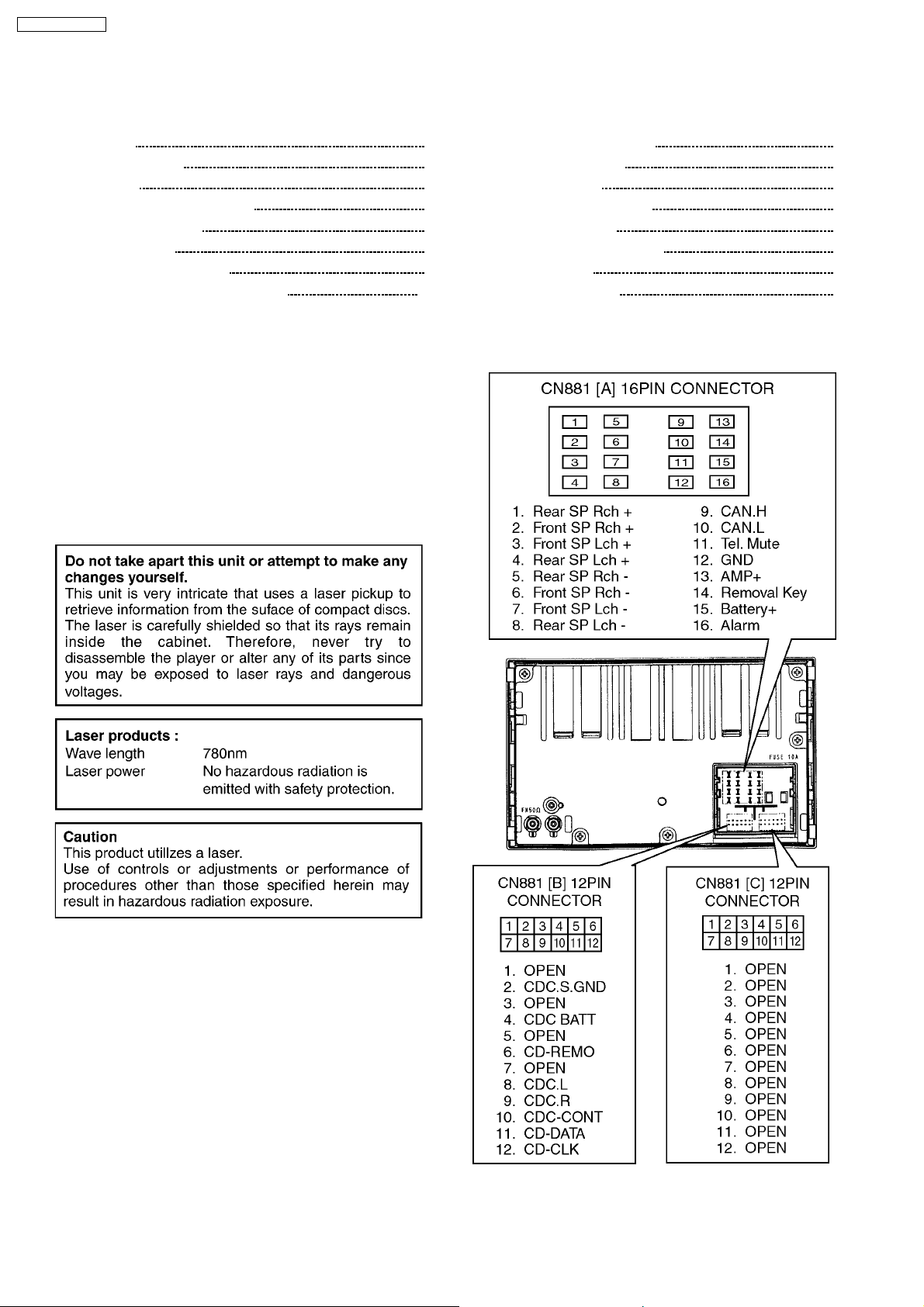
5 WIRING CONNECTION
4
Page 5
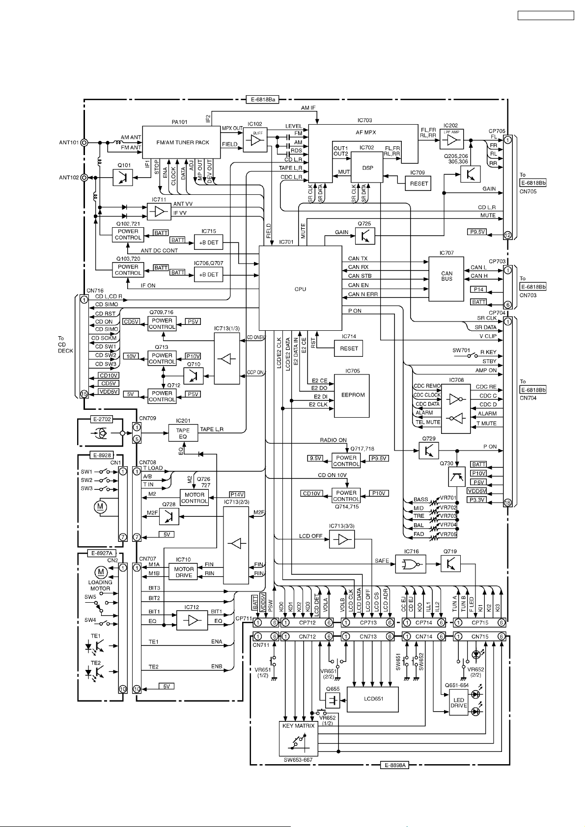
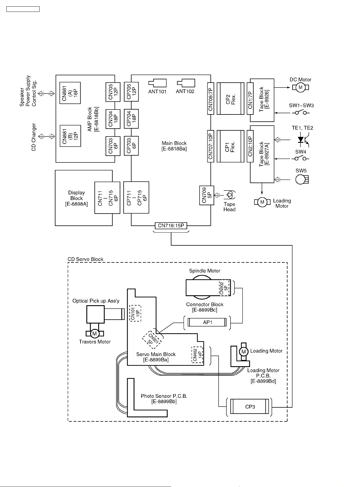
6 BLOCK DIAGRAM
6.1. Main Block
V.W. / CQ-JV1060L
5
Page 6
V.W. / CQ-JV1060L
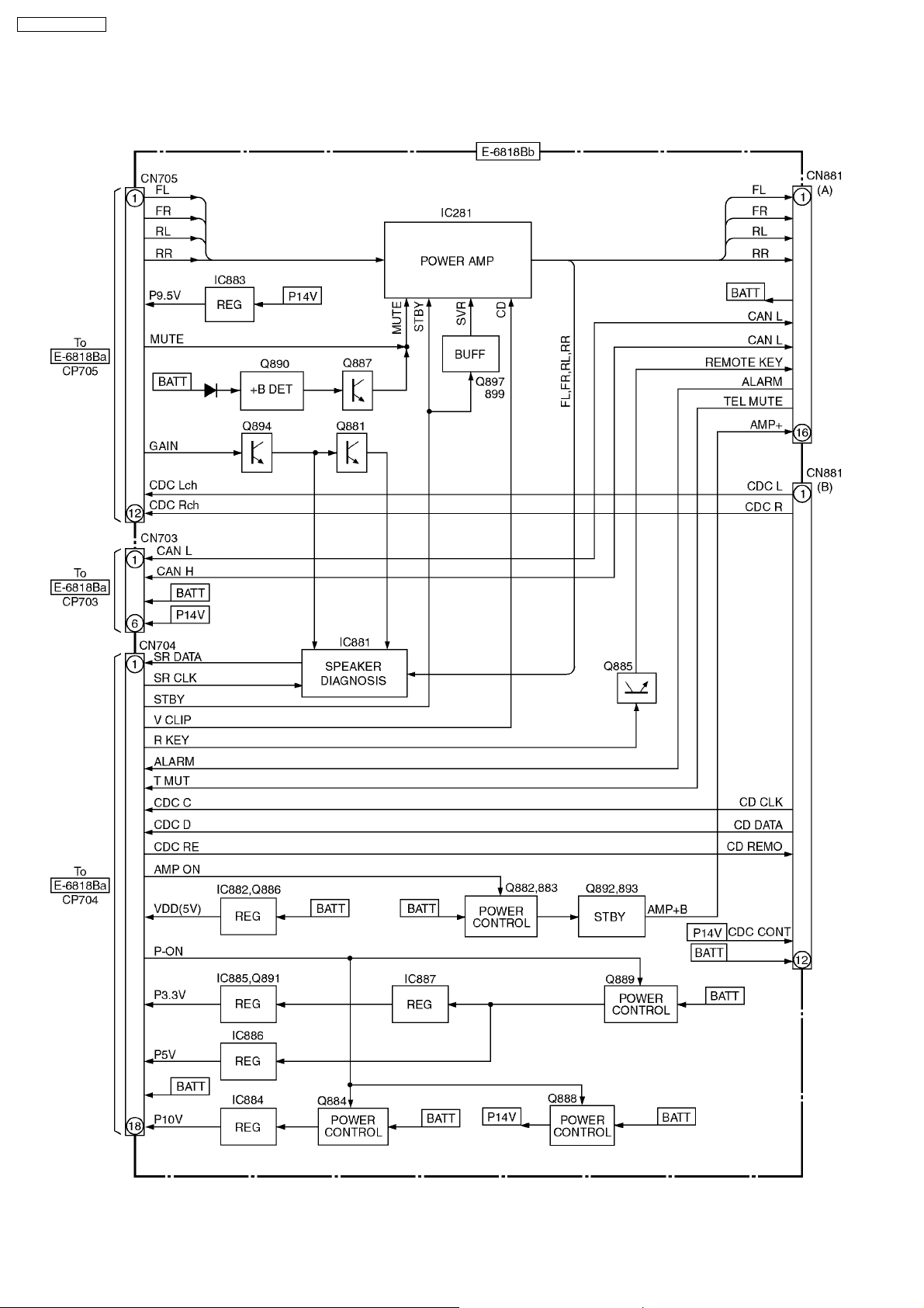
6.2. AMP Block
6
Page 7
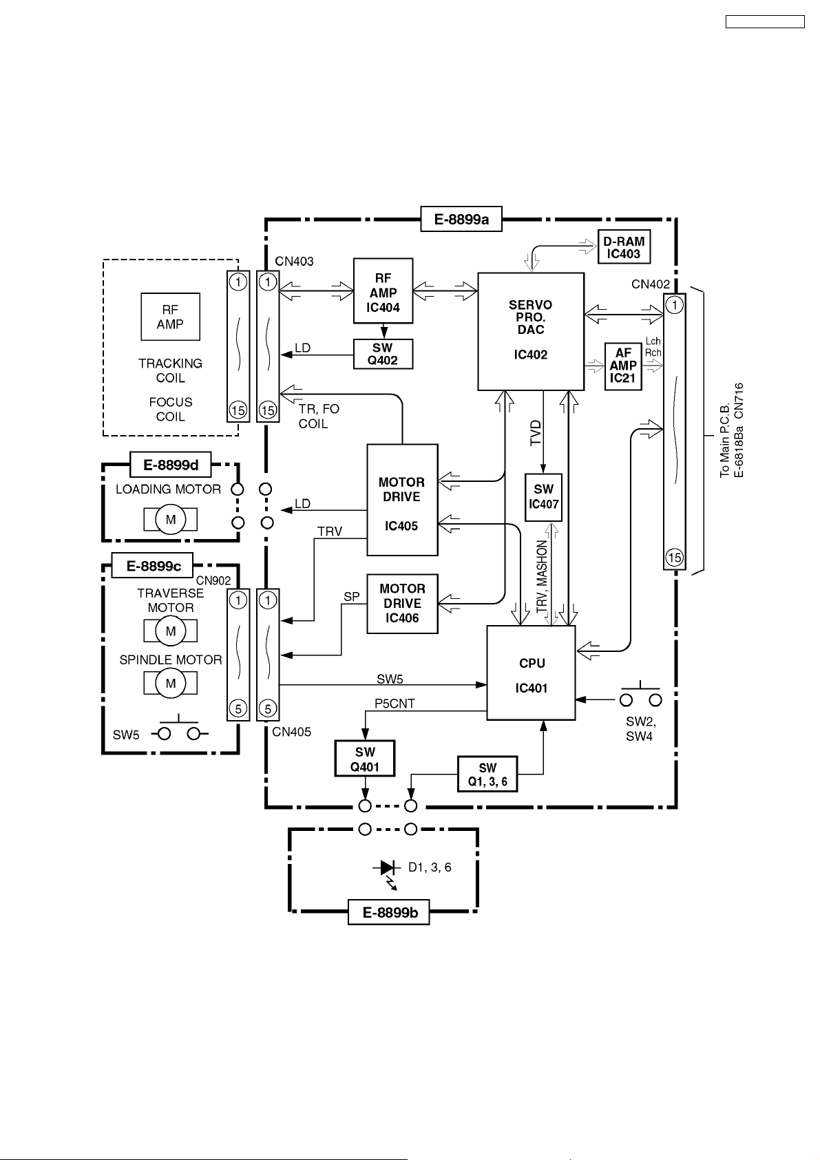
6.3. CD Servo Block
V.W. / CQ-JV1060L
7
Page 8
V.W. / CQ-JV1060L
7 TERMINALS DESCRIPTION
7.1. Main Block
IC701 : C2CBK A00001
Pin
No.
1 RSTOUT Not used - -
2 NMI (VDD pull-up) - 4.8
3 VSS Ground - 0
4 VDD +5V power supply - 4.8
5 LCD.ADR LCD addrress O 0
6 CD.SW3 CD disc out I 4.4
7 CD.SW1 CD disc in I 4.5
8 P.ON System power on O 4.8
9 CAN6.1V Battery level detection (6.1V) I 4.7
10 SAFE Safety LED control O 4.8
11 ILL2 Illumi. on (LCD) O 4.8
12 ILL Illumi. on (Button) O 4.8
13 KI0 Key data input I 0
14 KI1 Key data input I 0
15 KI2 Key data input I 0
16 KI3 Key data input I 0
17 VSS Ground - 0
18 VDD +5V power supply - 4.8
19 SR.DATA Serial data I/O 4.8
20 SR.CLK Clock for serial data O 4.8
21 ANT.CNT ANT1 amp power control O 0
22 A/B.IN Tape side detection I 4.7
23 TUN.A Tuning/Scan SW I 0
24 TUN.B Tuning/Scan SW I 0
25 VSS Ground - 0
26 VDD +5V power supply - 4.8
27 DEV FM deviation I 0
28 ADJ FM adjacent interference I 0
29 M.P FM multipath interference I 0
30 FILD Fieldstrength level I 0.5
31 IF.V ANT2 current intensity I 0.5
32 ANT.V ANT1 current intensity I 0.5
33 BATT.V Battery level detection I 2.6
34 FAD Fader level I 2.3
35 VA.REF +5V power supply - 4.8
36 VA.GND Ground - 0
37 BAL Balance level I 2.3
38 TRE Treble level I 0
39 MID Middle level I 1.0
40 BASS Bass level I 1.0
41 VSS Ground - 0
42 VDD +5V power supply - 4.8
43 BAT.DET Battery level detection I 4.8
44 CC.EJ Tape eject I 4.8
45 CD.EJ CD eject I 1.8
46 ALARM Alarm signal I 0
47 P.SW Power on SW I 4.8
48 CD.SW2 CD SW2 input I 0
49 T.LOAD Tape loading detection I 0
50 DIAG.CONT Not used - -
51 VSS Ground - 0
52 VDD +5V power supply - 4.8
53 IF.ON ANT2 amp power control O 0
54 RADIO.ON Radio power control O 4.8
55 DSP.DET DSP in activity I 4.8
56 CD.RST CD reset O 4.8
57 CD.SIM0 CD serial data O 0
58 CD.ON CD controller enable O 0
59 BIT3 Tape mode SW I 0
60 BIT2 Tape mode SW I 0
61 CDC.REMO CD.CH remocon data O 0
62 CDC.DATA CD.CH data I 0
63 BIT1 Tape mode SW I 0
64 EQ Metal tape detection I
65 MS MS detection I 0
66 CDC.CLK Shift clock for CD.CH data O 0
67 LCD.DET LCD driver in activity I 0
Port Descriptions I/O Vol.
(V)
Pin
No.
68 VDD +5V power supply - 4.8
69 VSS Ground - 0
70 CD.SOMI CD serial data I 0
71 /T.MUT Telephon mute I 0
72 CD.SCKM Shift clock for CD data O 0
73 CAN.EN CAN BUS enable O 0
74 CAN.STB CAN BUS strobe O 0
75 CAN.RX CAN BUS data I 4.8
76 CAN.TX CAN BUS data O 4.8
77 CAN.N.ERR CAN BUS error I 4.8
78 VDD +5V power supply - 4.8
79 VSS Ground - 0
80 /RD Not used - -
81 /WR Not used - -
82 /READY Not used - -
83 ALE Not used - -
84 /EA (VDD pull-up) - 0
85 K00 Key scan O 1.2
86 K01 Key scan O 1.2
87 K02 Key scan O 0
88 K03 Key scan O 1.2
89 PL04 Not used - -
90 R.IN Tape reverse O 0
91 T.IN Tape-in detection I 0
92 ENDA Tape end detection I 0
93 VDD +5V power supply - 4.8
94 VSS Ground - 0
95 CD.ON10V CD power on (10V) O 4.6
96 M2F Main motor control O 4.8
97 CC.ON Tape power on O 0
98 ENDB Tape end detection I 0
99 GAIN Audio output level control O 4.8
100 CD.ON5V CD power on (5V) O 4.8
101 F.IN Tape forword O 0
102 LCD.ON LCD driver reset O 4.8
103 E2DATA Security data I 0
104 ST-BY Power amp stand-by O 4.8
105 DSP.RST DSP reset O 4.8
106 AMP.ON External AMP power on O 0
107 MUT Not used - 4.8
108 M2 Main motor control O 0
109 VOL.A Volume control signal I 0
110 VOL.B Volume control signal I 0
111 VDD +5V power supply - 4.8
112 VSS Ground - 0
113 E2CE Security ROM chip enable O 0
114 LCD/E2 DT LCD/Security data O 0
115 LCD/E2 CK Clock for LCD/Security data O 0
116 LCD CS2 LCD driver select O 0
117 F/E.STP Radio stopsignal input I 0.9
118 F/E.DATA Tuner control data O 0
119 F/E.ENA Tuner enable O 0
120 F/E.CLK Shift clock for control data O 0
121 VDD +5V power supply - 4.8
122 VSS Ground - 0
123 XTAL2 Crystal oscillator - 2.0
124 XTAL1 Crystal osdillator - 2.3
125 VSS Ground - 0
126 XTAL3 Crystal oscillator - 2.3
127 XTAL4 Crystal oscillator - 2.3
128 RST Reset I 4.9
Port Descriptions I/O Vol.
(V)
Note 1 : Voltage measuerments are with respect to ground,
with a voltmeter (internal resistance : 10M ohms).
8
Page 9
V.W. / CQ-JV1060L
7.2. CD Servo Block
IC402 : MN662783RPW
Pin
No.
1 VDD +5V power supply - 5.0
2 D0 D-RAM data I/O 2.3
3 D1 D-RAM data I/O 1.8
4 NWE D-RAM data write O 4.9
5 NRAS D-RAM row address strobe O 3.4
6 D2 D-RAM data I/O 0.8
7 D3 D-RAM data I/O 0
8 NCAS0 D-RAM columun address strobe O 3.9
9 A10 D-RAM address O 3.9
10 A8 D-RAM address O 0.6
11 A7 D-RAM address O 1.1
12 A6 D-RAM address O 0.7
13 A5 D-RAM address O 0
14 A4 D-RAM address O 1.1
15 A9 D-RAM address O 0.4
16-18 A0 D-RAM address O 1.0
19 A3 D-RAM address O 0
20 DVSS Ground - 0
21 DVDD +5V power supply - 5.0
22,23 - Not used - -
24 TVD Traverse motor control O 2.5
25 PC Not used - -
26 ECS Spindle motor control O 2.4
27 TRD Tracking coil drive O 2.5
28 FOD Focus coil drive O 2.4
29 FBAL Focus balance O 1.9
30 TBAL Tracking balance O 3.0
31 VREF Refence voltage I 2.5
32 FE Focus error I 2.5
33 TE Tracking error I 2.5
34 RFENV RF envelope I 2.5
35 OFTR Off track signal I 0
36 /RFDET RF detecting signal I 0
37 BDO Drop-out signal I 0
38 LDON Laser on signal O 4.5
39 ARF RF signal I 2.5
40 IREF Reference current input I 1.2
41 DRF Bias for DSL I 2.4
42 DSLF Loop filter for DSL I/O 2.5
43 DSLF2 Loop filter for DSL I/O 2.2
44 PLLF Loop filter for PLL I/O 1.4
45 VCOF Not used - -
46 AVDD +5V power supply - 5.0
47 AVSS Ground - 0
48 OUTL L channel output O 2.3
49 AVSS Ground - 0
50 OUTR R channel output O 2.3
51 AVDD +5V power supply - 4.7
52-54 - (Connecting to ground) - 0
55 FLAG Flag output O 0
56 FCLK Frame clock O 0
57-59 - Not used - -
60 TX Not used - -
61 MCLK Clock for I/F command I 1.0
62 MDATA Date for I/F command I 3.1
63 MLD I/F command load I 5.0
64 BLKCK Subcode block clock O 0
65 SQCK Ext.clock for sub code-Q I 5.0
66 SUBQ Code for sub. code-Q O 3.8
67 DMUTE Mute input I 0
68 STAT Status signal O 5.0
69 NRST Reset input I 5.0
70 CSEL (Connecting to ground) - 0
71 PMCK Clock output O 2.5
72 SMCK Clock output O 2.5
73 SUBC Serial data of sub code O 0
74 SBCK Shift clock for SUBC I 0.6
75 NCLDCK Not used - -
76 NTEST (Connecting to VDD) - 5.0
Port Descriptions I/O Vol.
(V)
Pin
No.
77 X1 Crystal oscillator - 0.4
78 X2 Crystal oscillator - 3.2
79 DVDD +5V power supply - 5.0
80 DVSS Ground - 0
Port Descriptions I/O Vol.
IC401 : MN101C30AAE
Pin
No.
1 SW4 Disc clamp detection I 0
2 SW5 Inner track detection I 5.0
3 SW2 Feeder arm detection I 4.8
4 PAG (Connecting to ground) - 0
5 IFR (Connecting to ground) - 0
6 VREF+ +5V power supply - 5.0
7 VDD +5V power supply - 5.0
8 OSC2 Crystal oscillator - 2.2
9 OSC1 Crystal oscillator - 2.1
10 VSS Ground - 0
11 XI (Connecting to ground) - 0
12 XO Not used - -
13 GND Ground - 0
14 SOMI CD changer serial data O 4.3
15 SIMO CD changer serial data I 1.3
16 SCKM Clock for serial data I 5.0
17 SB01 Not used - -
18 SUBQ Code for sub. code-Q I 1.6
19 SQCK Ext. clock for sub. code-Q O 5.0
20 P0G Not used - -
21 RST Reset input I 4.9
22 BD0 Drop-out signal I 0
23 PC1 Loading motor driver control O 5.0
24-26 - Not used - -
27 CDON CD activity I 5.0
28 BLKCK Subcode block clock O 0
29-31 - Not used - -
32 PC2 Focus/Tracking driver control O 0
33-36 - Not used - -
37 LOD Loading motor control I/O 2.5
38 TRV Traverse motor control I/O 2.4
39 NRST Servo IC reset O 5.0
40 STAT Status signal I 2.1
41 DMUTE DSP mute O 0
42-55 - Not used - -
56 MASHON Servo IC OSC control O 0.2
57 MCLK Command clock O 4.1
58 MDATA Command data O 3.1
59 MLD Command load O 5.0
60 P80 Not used - -
61 VREF- (Connecting to ground) - 0
62 Q1 Photo sensor signal (DISC IN) I 4.5
63 Q3 Photo sensor signal (DISC OUT) I 4.2
64 Q6 Photo sensor signal (Option) I 5.0
Port Descriptions I/O Vol.
(V)
(V)
9
Page 10

V.W. / CQ-JV1060L
8 PACKAGE AND IC BLOCK DIAGRAM
8.1. Main Block
IC705 : YEAMS292 2ADF
PA101 : J3CCAB000001
IC102 : AN6564NST1
IC706 : YEAM2951MT
IC281 : C1BA00000314
IC710 : YEAMLB19 30MT
10
Page 11

IC707 : C1EB00000039
8.2. CD Servo Block
V.W. / CQ-JV1060L
IC714 : MN1382QTX
IC715 : C0EBM0000005
IC403 : C3ABMB000022
IC881 : C1EB00000042
11
Page 12

V.W. / CQ-JV1060L
IC404 : C1BB00000173
IC405 : C0GBY0000004
IC406 : C0GBY0000003
12
Page 13

V.W. / CQ-JV1060L
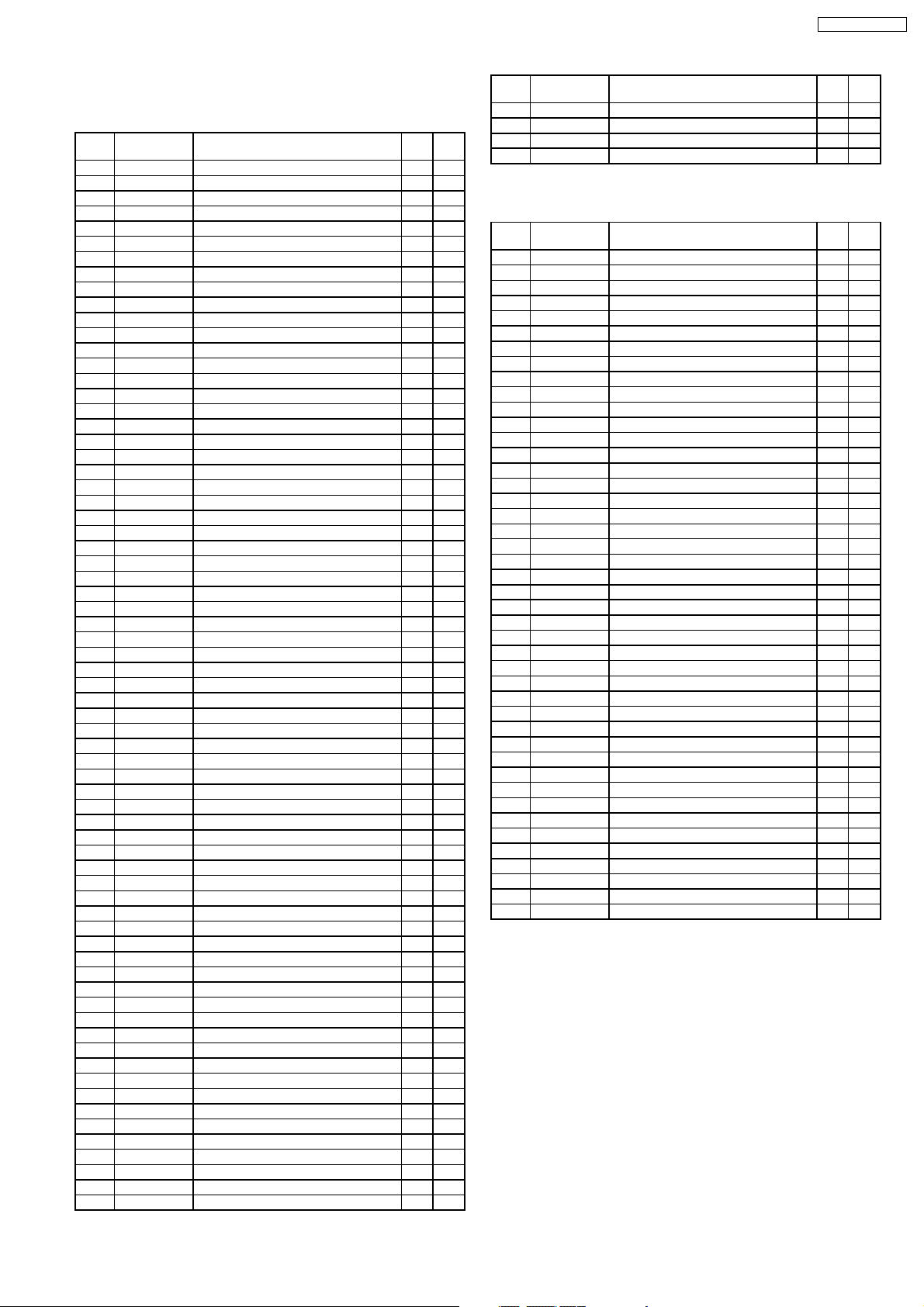
9 REPLACEMENT PARTS
LIST
Notes :
1. Be sure to make your orders of replacement parts
according to this list.
2. Important safety notice: Components, identified by
have special characteristics important for safety. When
replacing any of these components, use only
manufacturer´s specified parts.
3. Location keys in the remarks column indicates the general
location of the parts shown in the exploded drawing, as in a
road map.
4. The marking (RTL) indicates that Retention Time is limited
for this item. After the discontinuation of assembly in
production, the item will continue to be available for a
specific period of time. The retention period of availability is
dependent on the type of assembly, and in accordance with
the laws governing part and product retention. After the end
of this period, the assembly will no longer be available.
5. "MCC" marks in remarks column are indicated supply parts
of Matsushita Communication Industrial Corp. of America
(MCC).
Ref.
No.
[E6818B] Main/AMP Block
IC´s and TRANSISTORs
IC102 AN6564NST1 IC
IC201 YEAMTA7705FL IC
IC202 C0ABCB000005 IC
IC281 C1BA00000314 IC
IC701 C2CBKA000001 IC
IC702 C2HBZY000007 IC
IC703 C1BB00000408 IC
IC705 YEAMS2922ADF IC
IC706 YEAM2951MT IC
IC707 C1EB00000039 IC
IC708 YEAMC14584BE IC
IC709 MN1382JP IC
IC710 YEAMLB1930MT IC
IC711 C0ABBA000022 IC
IC712 YEAM74HC126F IC
IC713 C0JBAZ001229 IC
IC714 MN1382QTX IC
IC715 C0EBM0000005 IC
IC716 C0JBAD000030 IC
IC881 C1EB00000042 IC
IC882 C0DBZHZ00007 IC
IC883 AN7709F IC
IC884 YEAMPC2410HF IC
IC885 C0DBZGZ00005 IC
IC886 AN78N05 IC
IC887 AN7808 IC
PA101 J3CCAB000001 Electronic Tuner
Q101 B1ABBD000004 Transistor
Q102 B1GBCFNN0005 Transistor
Q103 B1GBCFNN0005 Transistor
Q205 YEANC314TKTX Transistor
Q206 YEANC314TKTX Transistor
Q305 YEANC314TKTX Transistor
Q306 YEANC314TKTX Transistor
Q707 YEAN2SK1133T Transistor
Q709 B1GBCFJN0005 Transistor
Q710 B1GBCFJN0005 Transistor
Q712 YEANFP1F3PT1 Transistor
Q713 YEANFP1F3PT1 Transistor
Q714 2SB1073TX Transistor
Q715 B1GBCFJN0005 Transistor
Part No. Part Name & Description Remarks
mark
Ref.
No.
Q716 B1ADJC000003 Transistor
Q717 B1ADJC000003 Transistor
Q718 B1GBCFJN0005 Transistor
Q719 B1ABCF000044 Transistor
Q720 YEANFP1F3PT1 Transistor
Q721 2SB1073TX Transistor
Q725 YEANA114EKTX Transistor
Q726 B1GBCFJN0005 Transistor
Q727 2SB1073TX Transistor
Q728 B1GBCFNN0005 Transistor
Q729 YEANC3661TA Transistor
Q730 YEANA114EKTX Transistor
Q881 B1ABCF000044 Transistor
Q882 B1GBCFJN0005 Transistor
Q883 B1ADJC000003 Transistor
Q884 2SB1073TX Transistor
Q885 B1ABCF000044 Transistor
Q886 2SB946 Transistor
Q887 B1GBCFNN0005 Transistor
Q888 2SB1073TX Transistor
Q889 2SB1073TX Transistor
Q890 B1ABCF000042 Transistor
Q891 2SB1193 Transistor
Q892 2SD1328STTX Transistor
Q893 B1BBAC000007 Transistor
Q894 B1GBCFNN0005 Transistor
Q897 B1GBCFNN0005 Transistor
Q899 YEANC3661TA Transistor
DIODEs
D101 MAZ33600ML Diode
D102 MAZ33600ML Diode
D702 YEAD1SS355T1 Diode
D703 YEAD1SS355T1 Diode
D704 YEAD1SS355T1 Diode
D705 YEAD1SS355T1 Diode
D707 YEAD1SS355T1 Diode
D708 YEAD1SS355T1 Diode
D709 YEAD1SS355T1 Diode
D710 YEAD1SS355T1 Diode
D711 MA721TX Diode
D712 YEAD1SS355T1 Diode
D713 YEAD1SS355T1 Diode
D720 MA8056LMHTX Diode
D721 MA153TX Diode
D722 YEAD1SS355T1 Diode
D723 YEAD1SS355T1 Diode
D724 YEAD1SS355T1 Diode
D725 YEAD1SS355T1 Diode
D726 MA8100LMTX Diode
D729 YEAD1SS355T1 Diode
D733 MA8051MTX Diode
D737 MA151WKTX Diode
D739 MA151WATX Diode
D740 MA8051MTX Diode
D741 MA8051MTX Diode
D742 YEAD1SS355T1 Diode
D743 YEAD1SS355T1 Diode
D744 YEAD1SS355T1 Diode
D745 YEAD1SS355T1 Diode
D746 MA8056LMHTX Diode
D747 YEAD1SS355T1 Diode
D748 YEAD1SS355T1 Diode
D749 YEAD1SS355T1 Diode
D750 MA8056LMHTX Diode
D751 MA8056LMHTX Diode
D752 MAZ816000L Diode
D753 MAZ816000L Diode
D754 YEAD1SS355T1 Diode
D881 YEADDSM3MA2T Diode
D882 YEAD1SS355T1 Diode
D883 YEAD1SS355T1 Diode
Part No. Part Name & Description Remarks
13
Page 14

V.W. / CQ-JV1060L
Ref.
No.
D885 MA151WKTX Diode
D886 YEAD1SS355T1 Diode
D889 MA8051MTX Diode
D890 MA8051MTX Diode
D891 MA8051MTX Diode
D892 YEAD1SS355T1 Diode
D893 YEADDSM3MA2T Diode
D897 YEADF10P04Q Diode
D899 YEAD1SS355T1 Diode
D900 YEAD1SS355T1 Diode
D901 YEADEC10DS1 Diode
CAPACITORs
C101 ECA1AM471B Electrolytic, 470µF 10WV
C102 YECUS1H103KX Ceramic, 0.01µF 50WV
C103 YECUS1H103KX Ceramic, 0.01µF 50WV
C104 YECUS1H103KX Ceramic, 0.01µF 50WV
C105 YECUS1H103KX Ceramic, 0.01µF 50WV
C106 YECUS1H271JM Ceramic, 270PF 50WV
C107 YECUV2A103KX Ceramic, 0.01µF 100WV
C108 YECUV1H820JM Ceramic, 82PF 50WV
C109 ECA1AM471B Electrolytic, 470µF 10WV
C110 YECUS1H101JM Ceramic, 100PF 50WV
C111 YECUS1H102KX Ceramic, 0.001µF 50WV
C113 YECUS1H102KX Ceramic, 0.001µF 50WV
C114 YECUS1H102KX Ceramic, 0.001µF 50WV
C115 YECUS1H102KX Ceramic, 0.001µF 50WV
C116 YECUZ1C104KX Ceramic, 0.1µF 16WV
C117 YECUS1H102KX Ceramic, 0.001µF 50WV
C201 YECUZ1H332KX Ceramic, 0.0033µF 50WV
C202 ECEA1HKA2R2I Electrolytic, 2.2µF 50WV
C203 YECUZ1H471KX Ceramic, 470PF 50WV
C204 YECUZ1H471KX Ceramic, 470PF 50WV
C205 YECUZ1H821KX Ceramic, 820PF 50WV
C206 YECUS1H680JM Ceramic, 68PF 50WV
C207 ECEA1HKA2R2I Electrolytic, 2.2µF 50WV
C208 ECEA1HKA010I Electrolytic, 1µF 50WV
C209 ECEA1AKA470I Electrolytic, 47µF 10WV
C210 YECUZ1C104KX Ceramic, 0.1µF 16WV
C211 YECUS1H332KX Ceramic, 0.0033µF 50WV
C212 ECEA1HKA2R2I Electrolytic, 2.2µF 50WV
C213 YECUZ1H471KX Ceramic, 470PF 50WV
C214 YECUZ1H471KX Ceramic, 470PF 50WV
C215 YECUZ1H821KX Ceramic, 820PF 50WV
C216 YECUS1H680JM Ceramic, 68PF 50WV
C217 ECEA1HKA2R2I Electrolytic, 2.2µF 50WV
C218 ECEA1HKA010I Electrolytic, 1µF 50WV
C219 ECEA1CKA100I Electrolytic, 10µF 16WV
C220 YECUS1H103KX Ceramic, 0.01µF 50WV
C221 YECUS1H331JM Ceramic, 330PF 50WV
C222 YECUZ1H331JC Ceramic, 330PF 50WV
C223 YECUS1H123KX Ceramic, 0.012µF 50WV
C224 ECEA0JKA470I Electrolytic, 47µF 6.3WV
C225 YECUS1A105KX Ceramic, 1µF 10WV
C226 F1H0J1050010 Ceramic, 1µF 6.3WV
C228 F1H0J1050010 Ceramic, 1µF 6.3WV
C229 ECA1AM102B Electrolytic, 100µF 10WV
C230 ECEA1CKA100I Electrolytic, 10µF 16WV
C231 ECEA1CKA100I Electrolytic, 10µF 16WV
C232 ECEA1CKA100I Electrolytic, 10µF 16WV
C281 YECUS1C104KX Ceramic, 0.1µF 16WV
C282 ECA1CM101I Electrolytic, 100µF 16WV
C283 ECEA1HKA010I Electrolytic, 1µF 50WV
C292 YECUV1H221JM Ceramic, 220PF 50WV
C293 YECUV1H221JM Ceramic, 220PF 50WV
C294 YECUV1H221JM Ceramic, 220PF 50WV
C295 YECUV1H221JM Ceramic, 220PF 50WV
C296 YECUV1H101JM Ceramic, 100PF 50WV
C301 YECUS1H332KX Ceramic, 0.0033µF 50WV
C302 ECEA1HKA2R2I Electrolytic, 2.2µF 50WV
C303 YECUZ1H471KX Ceramic, 470PF 50WV
C304 YECUZ1H471KX Ceramic, 470PF 50WV
Part No. Part Name & Description Remarks
Ref.
No.
C305 YECUZ1H821KX Ceramic, 820PF 50WV
C306 YECUS1H680JM Ceramic, 68PF 50WV
C307 ECEA1HKA2R2I Electrolytic, 2.2µF 50WV
C308 ECEA1HKA010I Electrolytic, 1µF 50WV
C309 YECUS1C104KX Ceramic, 0.1µF 16WV
C310 ECEA1AKA220I Electrolytic, 22µF 10WV
C311 YECUZ1H332KX Ceramic, 0.0033µF 50WV
C312 ECEA1HKA2R2I Electrolytic, 2.2µF 50WV
C313 YECUS1H471JM Ceramic, 470PF 50WV
C314 YECUZ1H471KX Ceramic, 470PF 50WV
C315 YECUZ1H821KX Ceramic, 820PF 50WV
C316 YECUS1H680JM Ceramic, 68PF 50WV
C317 ECEA1HKA2R2I Electrolytic, 2.2µF 50WV
C318 ECEA1HKA010I Electrolytic, 1µF 50WV
C319 YECUS1A105KX Ceramic, 1µF 10WV
C320 F1H0J1050010 Ceramic, 1µF 6.3WV
C321 YECUZ1H331JC Ceramic, 330PF 50WV
C322 YECUS1H331JM Ceramic, 330PF 50WV
C323 YECUS1H123KX Ceramic, 0.012µF 50WV
C324 ECEA0JKA470I Electrolytic, 47µF 6.3WV
C325 YECUS1A105KX Ceramic, 1µF 10WV
C328 F1H0J1050010 Ceramic, 1µF 6.3WV
C381 ECA1CM222B Electrolytic, 2200µF 16WV
C383 ECEA1HKA010I Electrolytic, 1µF 50WV
C389 YECUS1C104KX Ceramic, 0.1µF 16WV
C392 YECUV1H221JM Ceramic, 220PF 50WV
C393 YECUV1H221JM Ceramic, 220PF 50WV
C394 YECUV1H221JM Ceramic, 220PF 50WV
C395 YECUV1H221JM Ceramic, 220PF 50WV
C396 YECUV1H101JM Ceramic, 100PF 50WV
C503 YECUS1H101JM Ceramic, 100PF 50WV
C507 YECUS1H101JM Ceramic, 100PF 50WV
C510 YECUS1H101JM Ceramic, 100PF 50WV
C511 YECUS1H101JM Ceramic, 100PF 50WV
C512 YECUS1H101JM Ceramic, 100PF 50WV
C701 YECUS1C104KX Ceramic, 0.1µF 16WV
C702 YECUS1C104KX Ceramic, 0.1µF 16WV
C703 YECUS1C104KX Ceramic, 0.1µF 16WV
C704 YECUS1C104KX Ceramic, 0.1µF 16WV
C705 YECUS1C104KX Ceramic, 0.1µF 16WV
C706 YECUS1C104KX Ceramic, 0.1µF 16WV
C707 YECUS1C104KX Ceramic, 0.1µF 16WV
C708 YECUS1C104KX Ceramic, 0.1µF 16WV
C709 YECUS1C104KX Ceramic, 0.1µF 16WV
C710 YECUS1C104KX Ceramic, 0.1µF 16WV
C711 YECUS1H220JM Ceramic, 22PF 50WV
C712 F1J1H120A034 Ceramic, 12PF 50WV
C713 ECA0JM221I Electrolytic, 220µF 6.3WV
C714 F1H1H101A231 Ceramic, 100PF 50WV
C715 YECUS1C104KX Ceramic, 0.1µF 16WV
C716 F1H1H101A231 Ceramic, 100PF 50WV
C717 ECEA1CSN100I Electrolytic, 10µF 16WV
C719 YECUS1C104KX Ceramic, 0.1µF 16WV
C722 ECEA1CKA100I Electrolytic, 10µF 16WV
C723 YECUS1H103KX Ceramic, 0.01µF 50WV
C724 YECUS1H103KX Ceramic, 0.01µF 50WV
C725 YECUS1A105KX Ceramic, 1µF 10WV
C726 YECUS1A105KX Ceramic, 1µF 10WV
C727 YECUS1H103KX Ceramic, 0.01µF 50WV
C728 YECUS1A105KX Ceramic, 1µF 10WV
C729 YECUS1H103KX Ceramic, 0.01µF 50WV
C730 YECUS1H103KX Ceramic, 0.01µF 50WV
C731 ECA1CM102B Electrolytic, 1000µF 16WV
C732 ECEA1CKA100I Electrolytic, 10µF 16WV
C733 ECEA1CKA100I Electrolytic, 10µF 16WV
C734 YECUZ1C104KX Ceramic, 0.1µF 16WV
C735 ECEA0JKA470I Electrolytic, 47µF 6.3WV
C736 YECUZ1C104KX Ceramic, 0.1µF 16WV
C737 ECEA0JKA470I Electrolytic, 47µF 6.3WV
C738 YECUZ1C104KX Ceramic, 0.1µF 16WV
C739 ECEA0JKA470I Electrolytic, 47µF 6.3WV
C740 YECUZ1H332KX Ceramic, 0.0033µF 50WV
C741 YECUZ1H332KX Ceramic, 0.0033µF 50WV
Part No. Part Name & Description Remarks
14
Page 15

V.W. / CQ-JV1060L
Ref.
No.
C742 YECUZ1H331JC Ceramic, 330PF 50WV
C743 YECUZ1H331JC Ceramic, 330PF 50WV
C744 YECUZ1A224KX Ceramic, 0.22µF 10WV
C745 YECUZ1A224KX Ceramic, 0.22µF 10WV
C748 YECUZ1A224KX Ceramic, 0.22µF 10WV
C749 YECUZ1A224KX Ceramic, 0.22µF 10WV
C750 YECUS1C224KX Ceramic, 0.22µF 16WV
C751 YECUZ1C104KX Ceramic, 0.1µF 16WV
C752 ECEA0JKA470I Electrolytic, 47µF 6.3WV
C753 YECUS1A105KX Ceramic, 1µF 10WV
C754 YECUS1A105KX Ceramic, 1µF 10WV
C755 ECA1CM101I Electrolytic, 100µF 16WV
C757 F1H1H100A226 Ceramic, 10PF 50WV
C758 F1H1H100A226 Ceramic, 10PF 50WV
C759 ECEA1CKA100I Electrolytic, 10µF 16WV
C762 F1H1H101A231 Ceramic, 100PF 50WV
C763 F1H1H101A231 Ceramic, 100PF 50WV
C764 F1H1H101A231 Ceramic, 100PF 50WV
C765 F1H1H101A231 Ceramic, 100PF 50WV
C766 YECUS1E223KX Ceramic, 0.022µF 25WV
C768 ECA1CM331B Electrolytic, 330µF 16WV
C769 YECUZ1C104KX Ceramic, 0.1µF 16WV
C770 YECUS1E473KX Ceramic, 0.047µF 25WV
C772 YECUZ1H103KX Ceramic, 0.01µF 50WV
C774 ECA1CM102B Electrolytic, 1000µF 16WV
C775 ECA0JM471I Electrolytic, 470µF 6.3WV
C777 YECUS1C104KX Ceramic, 0.1µF 16WV
C778 YECUS1H101JM Ceramic, 100PF 50WV
C779 YECUS1H101JM Ceramic, 100PF 50WV
C780 YECUS1H101JM Ceramic, 100PF 50WV
C781 YECUS1H101JM Ceramic, 100PF 50WV
C782 YECUS1H101JM Ceramic, 100PF 50WV
C783 F1H1H3R0A255 Ceramic, 3PF 50WV
C784 F1H1H3R0A255 Ceramic, 3PF 50WV
C794 ECEA0JKA470I Electrolytic, 47µF 6.3WV
C795 YECUS1H101JM Ceramic, 100PF 50WV
C796 YECUS1H101JM Ceramic, 100PF 50WV
C797 YECUS1A105KX Ceramic, 1µF 10WV
C799 YECUS1H103KX Ceramic, 0.01µF 50WV
C801 ECA0JM101I Electrolytic, 100µF 6.3WV
C802 F4D554730015 Electrolytic, 0.047F 5.5WV
C803 F4D554730015 Electrolytic, 0.047F 5.5WV
C804 F4D554730015 Electrolytic, 0.047F 5.5WV
C805 F4D554730015 Electrolytic, 0.047F 5.5WV
C806 YECUS1H103KX Ceramic, 0.01µF 50WV
C807 YECUZ1H103KX Ceramic, 0.01µF 50WV
C808 YECUZ1H103KX Ceramic, 0.01µF 50WV
C809 YECUZ1H103KX Ceramic, 0.01µF 50WV
C810 YECUS1A105KX Ceramic, 1µF 10WV
C866 YECUS1H103KX Ceramic, 0.01µF 50WV
C867 YECUS1C104KX Ceramic, 0.1µF 16WV
C868 YECUS1C104KX Ceramic, 0.1µF 16WV
C869 EEUFC1C681B Electrolytic, 680µF 16WV
C870 ECA1CM100I Electrolytic, 10µF 16WV
C871 YECUZ1C104KX Ceramic, 0.1µF 16WV
C872 YECUZ1C104KX Ceramic, 0.1µF 16WV
C873 YECUS1H103KX Ceramic, 0.01µF 50WV
C874 YECUS1E223KX Ceramic, 0.022µF 25WV
C875 YECUV1H681JM Ceramic, 680PF 50WV
C876 YECUV1H681JM Ceramic, 680PF 50WV
C877 YECUV1H101JM Ceramic, 100PF 50WV
C881 ECA1CM100I Electrolytic, 10µF 16WV
C882 ECA1AM102B Electrolytic, 1000µF 10WV
C883 YECUS1C104KX Ceramic, 0.1µF 16WV
C884 ECA1CM470I Electrolytic, 47µF 16WV
C885 YECUS1C104KX Ceramic, 0.1µF 16WV
C886 YECUS1C104KX Ceramic, 0.1µF 16WV
C887 YECUS1C104KX Ceramic, 0.1µF 16WV
C888 EEUFC1C820 Electrolytic, 82µF 16WV
C889 ECA1AM102B Electrolytic, 1000µF 10WV
C890 ECA1AM102B Electrolytic, 1000µF 10WV
C891 ECA1HM4R7I Electrolytic, 4.7µF 50WV
C892 ECA1AM102B Electrolytic, 1000µF 10WV
Part No. Part Name & Description Remarks
Ref.
No.
C895 ECA1CM102B Electrolytic, 1000µF 16WV
C896 YECUS1C104KX Ceramic, 0.1µF 16WV
C897 YECUS1C104KX Ceramic, 0.1µF 16WV
C898 ECA0JM101I Electrolytic, 100µF 6.3WV
C899 ECA0JM101I Electrolytic, 100µF 6.3WV
C901 ECA1CM101I Electrolytic, 100µF 16WV
C902 ECA1CM102B Electrolytic, 1000µF 16WV
C903 ECEA1EKA4R7I Electrolytic, 4.7µF 25WV
C904 YECUV1H101JM Ceramic, 100PF 50WV
C905 YECUV1H101JM Ceramic, 100PF 50WV
C906 YECUV1H101JM Ceramic, 100PF 50WV
C907 YECUS1C104KX Ceramic, 0.1µF 16WV
C908 YECUV1H681JM Ceramic, 680PF 50WV
C909 YECUV1H681JM Ceramic, 680PF 50WV
C910 ECA1CM222B Electrolytic, 2200µF 16WV
C911 ECA1CM222B Electrolytic, 2200µF 16WV
RESISTORs
J701 ERJ6GEY0R00 Chip, 0
J702 ERJ6GEY0R00 Chip, 0
J703 ERJ6GEY0R00 Chip, 0
J704 ERJ6GEY0R00 Chip, 0
J705 ERJ6GEY0R00 Chip, 0
J706 ERJ6GEY0R00 Chip, 0
J707 ERJ6GEY0R00 Chip, 0
L725 ERJ6GEY0R00 Chip, 0
L728 ERJ6GEY0R00 Chip, 0
L731 ERJ6GEY0R00 Chip, 0
L732 ERJ6GEY0R00 Chip, 0
L733 ERJ6GEY0R00 Chip, 0
R101 ERJ6GEYJ102 Chip, 1k
R102 ERJ6GEYJ102 Chip, 1k
R103 ERJ6GEYJ102 Chip, 1k
R106 ERJ6GEYJ183 Chip, 18k
R107 ERJ6GEYJ681 Chip, 680
R108 ERJ6GEYJ183 Chip, 18k
R109 ERJ6GEYJ223 Chip, 22k
R110 ERJ6GEYJ183 Chip, 18k
R111 ERJ6GEYJ561 Chip, 560
R112 ERJ3GEYJ102V Chip, 1k
R114 ERJ6GEYJ102 Chip, 1k
R115 ERJ6GEY0R00 Chip, 0
R116 ERJ6GEY0R00 Chip, 0
R117 ERJ6GEY0R00 Chip, 0
R119 ERJ6GEYJ105 Chip, 1M
R120 ERJ6GEYJ105 Chip, 1M
R201 ERJ3GEYJ103V Chip, 10k
R202 ERJ3GEYJ103V Chip, 10k
R203 ERJ6GEYJ103 Chip, 10k
R204 ERJ6GEYJ124 Chip, 120k
R205 ERJ6GEYJ103 Chip, 10k
R206 ERJ6GEYJ332 Chip, 3.3k
R207 ERJ3GEYJ392V Chip, 3.9k
R209 ERJ6GEYJ391 Chip, 390
R210 ERJ3GEYJ392V Chip, 3.9k
R211 ERJ3GEYJ103V Chip, 10k
R212 ERJ3GEYJ103V Chip, 10k
R213 ERJ3GEYJ103V Chip, 10k
R214 ERJ6GEYJ124 Chip, 120k
R215 ERJ6GEYJ103 Chip, 10k
R216 ERJ6GEYJ332 Chip, 3.3k
R217 ERJ3GEYJ392V Chip, 3.9k
R219 ERJ6GEYJ391 Chip, 390
R220 ERJ3GEYJ392V Chip, 3.9k
R221 ERJ6GEYJ124 Chip, 120k
R222 ERJ3GEYJ124V Chip, 120k
R223 ERJ6GEYJ183 Chip, 18k
R224 ERJ6GEYJ123 Chip, 12k
R225 ERJ6GEYJ334 Chip, 330k
R226 ERJ6GEYJ121 Chip, 120
R227 ERJ6GEYJ102 Chip, 1k
R228 ERJ6GEYJ122 Chip, 1.2k
Part No. Part Name & Description Remarks
ΩΩΩΩ
1/10W
ΩΩΩΩ
1/10W
ΩΩΩΩ
1/10W
ΩΩΩΩ
1/10W
ΩΩΩΩ
1/10W
ΩΩΩΩ
1/10W
ΩΩΩΩ
1/10W
ΩΩΩΩ
1/10W
ΩΩΩΩ
1/10W
ΩΩΩΩ
1/10W
ΩΩΩΩ
1/10W
ΩΩΩΩ
1/10W
ΩΩΩΩ
1/10W
ΩΩΩΩ
1/10W
ΩΩΩΩ
1/10W
ΩΩΩΩ
1/10W
ΩΩΩΩ
1/10W
ΩΩΩΩ
1/10W
ΩΩΩΩ
1/10W
ΩΩΩΩ
1/10W
ΩΩΩΩ
1/10W
ΩΩΩΩ
1/16W
ΩΩΩΩ
1/10W
ΩΩΩΩ
1/10W
ΩΩΩΩ
1/10W
ΩΩΩΩ
1/10W
ΩΩΩΩ
1/10W
ΩΩΩΩ
1/10W
ΩΩΩΩ
1/16W
ΩΩΩΩ
1/16W
ΩΩΩΩ
1/10W
ΩΩΩΩ
1/10W
ΩΩΩΩ
1/10W
ΩΩΩΩ
1/10W
ΩΩΩΩ
1/16W
ΩΩΩΩ
1/10W
ΩΩΩΩ
1/16W
ΩΩΩΩ
1/16W
ΩΩΩΩ
1/16W
ΩΩΩΩ
1/16W
ΩΩΩΩ
1/10W
ΩΩΩΩ
1/10W
ΩΩΩΩ
1/10W
ΩΩΩΩ
1/16W
ΩΩΩΩ
1/10W
ΩΩΩΩ
1/16W
ΩΩΩΩ
1/10W
ΩΩΩΩ
1/16W
ΩΩΩΩ
1/10W
ΩΩΩΩ
1/10W
ΩΩΩΩ
1/10W
ΩΩΩΩ
1/10W
ΩΩΩΩ
1/10W
ΩΩΩΩ
1/10W
15
Page 16

V.W. / CQ-JV1060L
Ref.
No.
R283 ERJ3GEYJ822V Chip, 8.2k
R291 ERJ3GEYJ473V Chip, 47k
R292 ERJ14YJ821H Chip, 820
R293 ERJ14YJ821H Chip, 820
R301 ERJ3GEYJ103V Chip, 10k
R302 ERJ3GEYJ103V Chip, 10k
R303 ERJ3GEYJ103V Chip, 10k
R304 ERJ6GEYJ124 Chip, 120k
R305 ERJ6GEYJ103 Chip, 10k
R306 ERJ6GEYJ332 Chip, 3.3k
R307 ERJ3GEYJ392V Chip, 3.9k
R309 ERJ6GEYJ391 Chip, 390
R310 ERJ3GEYJ392V Chip, 3.9k
R311 ERJ3GEYJ103V Chip, 10k
R312 ERJ3GEYJ103V Chip, 10k
R313 ERJ3GEYJ103V Chip, 10k
R314 ERJ6GEYJ124 Chip, 120k
R315 ERJ6GEYJ103 Chip, 10k
R316 ERJ6GEYJ332 Chip, 3.3k
R317 ERJ3GEYJ392V Chip, 3.9k
R319 ERJ6GEYJ391 Chip, 390
R320 ERJ3GEYJ392V Chip, 3.9k
R321 ERJ3GEYJ124V Chip, 120k
R322 ERJ6GEYJ124 Chip, 120k
R323 ERJ6GEYJ183 Chip, 18k
R324 ERJ6GEYJ123 Chip, 12k
R325 ERJ6GEYJ334 Chip, 330k
R326 ERJ6GEYJ121 Chip, 120
R383 ERJ3GEYJ822V Chip, 8.2k
R391 ERJ3GEYJ473V Chip, 47k
R392 ERJ14YJ821H Chip, 820
R393 ERJ14YJ821H Chip, 820
R502 ERJ6GEYJ104 Chip, 100k
R503 ERJ6GEYJ102 Chip, 1k
R507 ERJ6GEYJ104 Chip, 100k
R508 ERJ6GEYJ103 Chip, 10k
R511 ERJ3GEY0R00V Chip, 0
R512 ERJ3GEYJ103V Chip, 10k
R514 ERJ6GEYJ822 Chip, 8.2k
R518 ERJ3GEYJ102V Chip, 1k
R519 ERJ6GEYJ102 Chip, 1k
R522 ERJ3GEYJ102V Chip, 1k
R523 ERJ6GEYJ103 Chip, 10k
R701 ERJ6GEYJ473 Chip, 47k
R702 ERJ6GEYJ473 Chip, 47k
R705 ERJ6GEYJ473 Chip, 47k
R706 ERJ6GEYJ473 Chip, 47k
R707 ERJ3GEYJ105V Chip, 1M
R708 ERJ3GEYJ105V Chip, 1M
R712 ERJ6GEYJ822 Chip, 8.2k
R713 ERJ6GEYJ473 Chip, 47k
R715 ERJ6GEYJ472 Chip, 4.7k
R716 ERJ6GEYJ472 Chip, 4.7k
R718 ERJ6GEYJ472 Chip, 4.7k
R719 ERJ6GEYJ472 Chip, 4.7k
R720 ERJ14YJ102H Chip, 1k
R721 ERJ3GEYJ223V Chip, 22k
R723 ERJ6GEYJ105 Chip, 1M
R724 ERJ3GEY0R00V Chip, 0
R725 ERJ6GEYJ102 Chip, 1k
R726 ERJ6GEYJ102 Chip, 1k
R727 ERJ6GEYJ102 Chip, 1k
R728 ERJ3GEYJ104V Chip, 100k
R730 ERJ3GEYJ104V Chip, 100k
R732 ERJ6GEYJ105 Chip, 1M
R733 ERJ3GEYJ102V Chip, 1k
R734 ERDS1FVJ1R0 Carbon, 1
R735 ERJ3GEYJ102V Chip, 1k
R736 ERJ3GEYJ102V Chip, 1k
R737 ERJ3GEYJ183V Chip, 18k
R738 ERJ3GEYJ104V Chip, 100k
R739 ERJ6GEYJ104 Chip, 100k
R740 ERJ6GEYJ104 Chip, 100k
Part No. Part Name & Description Remarks
ΩΩΩΩ
ΩΩΩΩ
ΩΩΩΩ
ΩΩΩΩ
ΩΩΩΩ
ΩΩΩΩ
ΩΩΩΩ
ΩΩΩΩ
ΩΩΩΩ
ΩΩΩΩ
ΩΩΩΩ
ΩΩΩΩ
ΩΩΩΩ
ΩΩΩΩ
ΩΩΩΩ
ΩΩΩΩ
ΩΩΩΩ
ΩΩΩΩ
ΩΩΩΩ
ΩΩΩΩ
ΩΩΩΩ
ΩΩΩΩ
ΩΩΩΩ
ΩΩΩΩ
ΩΩΩΩ
ΩΩΩΩ
ΩΩΩΩ
ΩΩΩΩ
ΩΩΩΩ
ΩΩΩΩ
ΩΩΩΩ
ΩΩΩΩ
ΩΩΩΩ
ΩΩΩΩ
ΩΩΩΩ
ΩΩΩΩ
ΩΩΩΩ
ΩΩΩΩ
ΩΩΩΩ
ΩΩΩΩ
ΩΩΩΩ
ΩΩΩΩ
ΩΩΩΩ
ΩΩΩΩ
ΩΩΩΩ
ΩΩΩΩ
ΩΩΩΩ
ΩΩΩΩ
1/10W
ΩΩΩΩ
ΩΩΩΩ
1/16W
ΩΩΩΩ
ΩΩΩΩ
1/16W
1/10W
1/16W
ΩΩΩΩ
ΩΩΩΩ
ΩΩΩΩ
ΩΩΩΩ
ΩΩΩΩ
1/16W
1/16W
ΩΩΩΩ
ΩΩΩΩ
ΩΩΩΩ
ΩΩΩΩ
ΩΩΩΩ
ΩΩΩΩ
1/4W
ΩΩΩΩ
ΩΩΩΩ
1/10W
1/16W
1/10W
1/10W
1/10W
ΩΩΩΩ
ΩΩΩΩ
ΩΩΩΩ
1/10W
1/16W
ΩΩΩΩ
1/16W
1/16W
ΩΩΩΩ
ΩΩΩΩ
ΩΩΩΩ
ΩΩΩΩ
1/16W
1/16W
1/4W
1/4W
1/16W
1/16W
1/16W
1/10W
1/10W
1/10W
1/16W
1/10W
1/16W
1/16W
1/16W
1/16W
1/10W
1/10W
1/10W
1/16W
1/10W
1/16W
1/16W
1/10W
1/10W
1/10W
1/10W
1/10W
1/16W
1/16W
1/4W
1/4W
1/10W
1/10W
1/10W
1/16W
1/10W
1/10W
1/10W
1/10W
1/10W
1/10W
1/10W
1/10W
1/10W
1/10W
1/10W
1/10W
1/16W
1/16W
1/16W
1W
1/16W
1/16W
1/10W
1/10W
Ref.
No.
R742 ERJ6GEYJ102 Chip, 1k
R743 ERJ6GEYJ473 Chip, 47k
R744 ERJ6GEYJ103 Chip, 10k
R745 ERJ3GEYJ105V Chip, 1M
R746 ERJ3GEYJ103V Chip, 10k
R747 ERJ3GEYJ124V Chip, 120k
R748 ERJ3GEYJ473V Chip, 47k
R749 ERJ3GEYJ104V Chip, 100k
R752 ERX1SJ6R8E Metal Film, 6.8
R753 ERJ6GEYJ100 Chip, 10
R754 ERJ3GEYJ561V Chip, 560
R755 ERJ6GEYJ561 Chip, 560
R756 ERJ6GEYJ104 Chip, 100k
R757 ERJ6GEYJ125 Chip, 1.2M
R758 ERJ6GEYJ125 Chip, 1.2M
R759 ERJ6GEYJ474 Chip, 470k
R760 ERJ3GEYJ105V Chip, 1M
R761 ERJ3GEYJ153V Chip, 15k
R762 ERJ6GEYJ103 Chip, 10k
R764 ERJ6ENF1202V Chip, 12k
R765 ERJ3GEYJ104V Chip, 100k
R766 ERJ6ENF1002 Chip, 10k
R767 ERJ3GEYJ682V Chip, 6.8k
R768 ERJ3GEYJ103V Chip, 10k
R769 ERJ6GEYJ684 Chip, 680k
R772 ERJ6GEYJ564 Chip, 560k
R774 ERJ6GEYJ104 Chip, 100k
R775 ERG1SJ680E Metal Oxid, 6.8
R776 ERJ3GEYJ102V Chip, 1k
R778 ERJ8GEYJ103V Chip, 10k
R779 ERJ6GEYJ222 Chip, 2.2k
R780 ERJ6GEYJ222 Chip, 2.2k
R781 ERJ6GEYJ103 Chip, 10k
R787 ERJ6GEYJ104 Chip, 100k
R788 ERJ6GEYJ473 Chip, 47k
R789 ERJ3GEYJ102V Chip, 1k
R790 ERJ3GEYJ223V Chip, 22k
R792 ERDS1FVJ1R5 Carbon, 1.5
R793 ERJ6GEYJ472 Chip, 4.7k
R794 ERJ6GEYJ472 Chip, 4.7k
R795 ERJ3GEYJ392V Chip, 3.9k
R796 ERJ3GEYJ392V Chip, 3.9k
R797 ERJ3GEYJ684V Chip, 680k
R798 ERJ3GEYJ564V Chip, 560k
R799 ERJ3GEYJ104V Chip, 100k
R800 ERJ3GEYJ104V Chip, 100k
R801 ERJ3GEYJ104V Chip, 100k
R802 ERJ3GEYJ104V Chip, 100k
R803 ERG1SJ680E Metal Oxid, 68
R804 ERG1SJ680E Metal Oxid, 68
R806 ERJ6GEYJ473 Chip, 47k
R808 ERJ8GEYJ103V Chip, 10k
R809 ERG1SJ271E Metal Oxid, 270
R810 ERG1SJ271E Metal Oxid, 270
R811 ERG1SJ271E Metal Oxid, 270
R813 ERJ3GEYJ223V Chip, 22k
R814 ERJ6GEYJ100 Chip, 10
R816 ERJ3GEYJ103V Chip, 10k
R818 ERJ3GEYJ184V Chip, 180k
R825 ERJ3GEYJ103V Chip, 10k
R828 ERJ3GEY0R00V Chip, 0
R829 ERJ6GEYJ103 Chip, 10k
R835 ERJ6GEYJ223 Chip, 22k
R836 ERJ8GEYJ222V Chip, 2.2k
R837 ERJ3GEYJ223V Chip, 22k
R838 ERJ8GEYJ471V Chip, 470
R843 ERJ3GEY0R00V Chip, 0
R844 ERJ6GEYJ685 Chip, 6.8M
R846 ERJ3GEY0R00V Chip, 0
R847 ERJ3GEY0R00V Chip, 0
R849 ERJ3GEY0R00V Chip, 0
R850 ERJ3GEY0R00V Chip, 0
R869 ERJ6GEYJ473 Chip, 47k
Part No. Part Name & Description Remarks
ΩΩΩΩ
1/10W
ΩΩΩΩ
1/10W
ΩΩΩΩ
1/10W
ΩΩΩΩ
1/16W
ΩΩΩΩ
1/16W
ΩΩΩΩ
1/16W
ΩΩΩΩ
1/16W
ΩΩΩΩ
1/16W
ΩΩΩΩ
1/10W
ΩΩΩΩ
1/16W
ΩΩΩΩ
1/10W
ΩΩΩΩ
1/10W
ΩΩΩΩ
1/10W
ΩΩΩΩ
1/10W
ΩΩΩΩ
1/10W
ΩΩΩΩ
1/16W
ΩΩΩΩ
1/16W
ΩΩΩΩ
1/10W
ΩΩΩΩ
1/10W
ΩΩΩΩ
1/16W
ΩΩΩΩ
1/10W
ΩΩΩΩ
1/16W
ΩΩΩΩ
1/16W
ΩΩΩΩ
1/10W
ΩΩΩΩ
1/10W
ΩΩΩΩ
1/10W
ΩΩΩΩ
1/16W
ΩΩΩΩ
1/8W
ΩΩΩΩ
1/10W
ΩΩΩΩ
1/10W
ΩΩΩΩ
1/10W
ΩΩΩΩ
1/10W
ΩΩΩΩ
1/10W
ΩΩΩΩ
1/16W
ΩΩΩΩ
1/16W
ΩΩΩΩ
ΩΩΩΩ
1/10W
ΩΩΩΩ
1/10W
ΩΩΩΩ
1/16W
ΩΩΩΩ
1/16W
ΩΩΩΩ
1/16W
ΩΩΩΩ
1/16W
ΩΩΩΩ
1/16W
ΩΩΩΩ
1/16W
ΩΩΩΩ
1/16W
ΩΩΩΩ
1/16W
ΩΩΩΩ
1/10W
ΩΩΩΩ
1/8W
ΩΩΩΩ
1/16W
ΩΩΩΩ
1/10W
ΩΩΩΩ
1/16W
ΩΩΩΩ
1/16W
ΩΩΩΩ
1/16W
ΩΩΩΩ
1/16W
ΩΩΩΩ
1/10W
ΩΩΩΩ
1/10W
ΩΩΩΩ
1/8W
ΩΩΩΩ
1/16W
ΩΩΩΩ
1/8W
ΩΩΩΩ
1/16W
ΩΩΩΩ
1/10W
ΩΩΩΩ
1/16W
ΩΩΩΩ
1/16W
ΩΩΩΩ
1/16W
ΩΩΩΩ
1/16W
ΩΩΩΩ
1/10W
ΩΩΩΩ
ΩΩΩΩ
1/2W
ΩΩΩΩ
ΩΩΩΩ
ΩΩΩΩ
ΩΩΩΩ
ΩΩΩΩ
1W
1W
1W
1W
1W
1W
1W
16
Page 17

V.W. / CQ-JV1060L
Ref.
No.
R871 ERJ6GEYJ102 Chip, 1k
R872 ERJ3GEYJ103V Chip, 10k
R873 ERJ8GEYJ102V Chip, 1k
R874 ERJ8GEYJ2R2V Chip, 2.2
R875 ERJ14YJ4R7H Chip, 4.7
R877 ERJ6GEYJ151 Chip, 150
R879 ERJ6GEYJ104 Chip, 100k
R880 ERJ6GEYJ102 Chip, 1k
R881 ERJ6GEYJ471 Chip, 470
R882 ERJ6GEYJ223 Chip, 22k
R883 ERJ6GEYJ104 Chip, 100k
R886 ERJ6GEYJ472 Chip, 4.7k
R887 ERJ3GEYJ103V Chip, 10k
R889 ERJ3GEYJ472V Chip, 4.7k
R890 ERJ8GX0R00V Chip, 0
R891 ERJ6GEY0R00 Chip, 0
R892 ERJ6GEYJ105 Chip, 1M
R894 ERJ6GEYJ222 Chip, 2.2k
R895 ERJ6GEYJ103 Chip, 10k
R897 ERJ6GEYJ102 Chip, 1k
R898 ERJ6GEYJ102 Chip, 1k
R899 ERJ6GEYJ102 Chip, 1k
R902 ERJ6GEY0R00 Chip, 0
R903 ERJ3GEYJ223V Chip, 22k
R904 ERJ8GEYJ222V Chip, 2.2k
R905 ERJ6GEYJ223 Chip, 22k
R906 ERJ8GEYJ222V Chip, 2.2k
R909 ERG1SJ121E Metal Oxid, 120
R911 ERJ6GEYJ103 Chip, 10k
R912 ERJ3GEYJ223V Chip, 22k
R913 ERJ8GEYJ222V Chip, 2.2k
R914 ERG1SJ121E Metal Oxid, 120
R915 ERG1SJ121E Metal Oxid, 120
R917 ERJ6GEYJ470 Chip, 47
R918 ERJ3GEYJ183V Chip, 18k
R919 ERJ3GEYJ472V Chip, 4.7k
R921 ERJ6GEY0R00 Chip, 0
R922 ERJ6GEYJ680 Chip, 68
R923 ERJ8GEYJ122V Chip, 1.2k
R924 ERJ6GEYJ103 Chip, 10k
R925 ERJ6GEYJ181 Chip, 180
R926 ERJ6GEYJ102 Chip, 1k
R929 ERJ8GEYJ222V Chip, 2.2k
R930 ERJ3GEYJ223V Chip, 22k
Part No. Part Name & Description Remarks
ΩΩΩΩ
1/10W
ΩΩΩΩ
1/16W
ΩΩΩΩ
1/8W
ΩΩΩΩ
1/8W
ΩΩΩΩ
1/4W
ΩΩΩΩ
1/10W
ΩΩΩΩ
1/10W
ΩΩΩΩ
1/10W
ΩΩΩΩ
1/10W
ΩΩΩΩ
1/10W
ΩΩΩΩ
1/10W
ΩΩΩΩ
1/10W
ΩΩΩΩ
1/16W
ΩΩΩΩ
1/16W
ΩΩΩΩ
1/8W
ΩΩΩΩ
1/10W
ΩΩΩΩ
1/10W
ΩΩΩΩ
1/10W
ΩΩΩΩ
1/10W
ΩΩΩΩ
1/10W
ΩΩΩΩ
1/10W
ΩΩΩΩ
1/10W
ΩΩΩΩ
1/10W
ΩΩΩΩ
1/16W
ΩΩΩΩ
1/8W
ΩΩΩΩ
1/10W
ΩΩΩΩ
1/8W
ΩΩΩΩ
1/10W
ΩΩΩΩ
1/16W
ΩΩΩΩ
1/8W
ΩΩΩΩ
1/10W
ΩΩΩΩ
1/16W
ΩΩΩΩ
1/16W
ΩΩΩΩ
1/10W
ΩΩΩΩ
1/10W
ΩΩΩΩ
1/8W
ΩΩΩΩ
1/10W
ΩΩΩΩ
1/10W
ΩΩΩΩ
1/10W
ΩΩΩΩ
1/8W
ΩΩΩΩ
1/16W
Ref.
No.
L101 YELT03NR15JT Coil
L102 ELER102KA Coil
L103 YELT03N4R7KT Coil
L104 G0ZZ00001907 Coil
L105 YELT45N4R7KT Coil
L106 J0JCC0000012 Coil
L107 G3A702C00001 Coil
L108 G1C5R6JA0005 Coil
L701 J0JCC0000012 Coil
L702 J0JCC0000012 Coil
L703 J0JCC0000012 Coil
L704 J0JCC0000012 Coil
L705 J0JCC0000012 Coil
L706 J0JCC0000012 Coil
L707 J0JCC0000012 Coil
L708 J0JCC0000012 Coil
L709 J0JCC0000012 Coil
L710 J0JCC0000012 Coil
L721 J0JCC0000012 Coil
L724 J0JCC0000012 Coil
L726 J0JCC0000012 Coil
L727 J0JCC0000012 Coil
L729 J0JCC0000012 Coil
L730 J0JCC0000012 Coil
L734 YELT03N4R7KT Coil
L736 J0JCC0000012 Coil
ΩΩΩΩ
1W
ΩΩΩΩ
1W
ΩΩΩΩ
1W
L881 YETQ026X163 Coil
L882 J0JCC0000012 Coil
L883 J0JCC0000012 Coil
L887 G0A111J00003 Coil
FILTERs
CS751 YECCL41P204T Filter
CS752 YECCL41P204T Filter
CS753 YECCL41P204T Filter
CS881 YECCL55S222T Filter
CRYSTALs
XL701 YEXL49U0419T Crystal
XL702 H0D855400002 Crystal
XL703 H0A327200019 Crystal
Part No. Part Name & Description Remarks
CONNECTORs
CN703 YEAETKCF06XY Connector, 6P
CN704 K1MQ18A00002 Connector, 18P
CN705 K1MQ12A00005 Connector, 12P
CN707 YEAE5280610 Connector, 10P
CN708 YEAE5280607 Connector, 7P
CN709 YEAE5280605 Connector, 5P
CN716 K1MN15A00007 Connector, 15P
CN881 K1FA440A0001 Connector
CP1 K9ZZ00000794 Flexible Cable, 10P
CP2 K9ZZ00000795 Flexible Cable, 7P
CP3 K9ZZ00000799 Flexible Cable, 5P
CP703 K1KA06B00133 Connector, 6P
CP704 K1KA18B00029 Connector, 18P
CP705 K1KA12B00105 Connector, 12P
CP711 K1KA06B00133 Connector, 6P
CP712 K1KA06B00133 Connector, 6P
CP713 K1KA06B00133 Connector, 6P
CP714 K1KA06B00133 Connector, 6P
CP715 K1KA06B00133 Connector, 6P
SWITCHEs
SW701 YEAS09277A Switch
COILs
LAMPs
Z101 J0LE00000002 ZNR
VARIABLE RESISTORs
VR701 D2BCD1520001 Variablr resistor
VR702 D2BCD1520001 Variablr resistor
VR703 D2BCD1520001 Variablr resistor
VR704 D2BCD1520001 Variablr resistor
VR705 D2BCD1520001 Variablr resistor
NETWORK RESISTORs
R520 EXBV8V102JV Network Resistor
R521 EXBV8V102JV Network Resistor
R709 EXBV8V102JV Network Resistor
R710 EXBV8V102JV Network Resistor
R717 EXBV8V104JV Network Resistor
R729 EXBV8V103JV Network Resistor
THERMISTOR
R777 YERT5BA1R8MT Thermistor
R812 YERT5BA1R8MT Thermistor
R878 YERT6AR4R7MT Thermistor
R910 YERT5BA1R8MT Thermistor
17
Page 18

V.W. / CQ-JV1060L
Ref.
No.
[E8898A] Display Block
IC´s and TRANSISTORs
Q651 B1GBCFNN0005 Transistor
Q652 YEANFP1F3PT1 Transistor
Q653 B1GBCFNN0005 Transistor
Q654 YEANFP1F3PT1 Transistor
Q655 YEAN2SK536TB Transistor
DIODEs
D651 B3AAB0000062 Diode
D652 B3AAB0000062 Diode
D653 B3AAB0000062 Diode
D654 B3AAB0000062 Diode
D655 B3AAB0000062 Diode
D656 B3AAB0000062 Diode
D657 B3AAB0000062 Diode
D658 B3AAB0000062 Diode
D659 B3AAB0000062 Diode
D660 B3AAB0000062 Diode
D661 B3AAB0000062 Diode
D662 B3AAB0000062 Diode
D663 B3AAB0000062 Diode
D664 B3AAB0000062 Diode
D665 B3AAB0000062 Diode
D666 B3AAB0000062 Diode
D667 B3AAB0000062 Diode
D668 B3AAB0000062 Diode
D669 B3AAB0000062 Diode
D670 B3AAB0000062 Diode
D671 B3AAB0000062 Diode
D672 B3AAB0000062 Diode
D673 B3AAB0000062 Diode
D674 B3AAB0000062 Diode
D675 B3AAB0000062 Diode
D676 B3AAB0000062 Diode
D677 B3AAB0000062 Diode
D678 B3AAB0000062 Diode
D679 B3AAB0000062 Diode
D680 B3AAB0000062 Diode
D681 B3AAB0000062 Diode
D682 B3AAB0000062 Diode
D683 B3AAB0000062 Diode
D684 B3AAB0000062 Diode
D685 YEAD1SS355T1 Diode
D686 B3AAB0000062 Diode
D687 B3AAB0000062 Diode
D688 MA8056LMHTX Diode
D689 B3AAB0000062 Diode
D691 B3AEB0000008 Diode
D692 B3AEB0000008 Diode
D693 B3AEB0000008 Diode
D694 B3AEB0000008 Diode
D695 B3AEB0000008 Diode
D696 B3AEB0000008 Diode
D697 B3AEB0000008 Diode
D698 B3AEB0000008 Diode
CAPACITORs
C651 YECUS1C105ZF Ceramic, 1µF 16WV
C652 YECUS1H103KX Ceramic, 0.01µF 50WV
C658 F1K1H104A033 Ceramic, 0.1µF 50WV
C659 F1K1H104A033 Ceramic, 0.1µF 50WV
C660 F1K1H104A033 Ceramic, 0.1µF 50WV
C661 F1K1H104A033 Ceramic, 0.1µF 50WV
C662 F1K1H104A033 Ceramic, 0.1µF 50WV
C664 YECUU1C335KX Tantalum, 3.3µF 16WV
C665 YECUU1C335KX Tantalum, 3.3µF 16WV
C666 YECUU1C335KX Tantalum, 3.3µF 16WV
Part No. Part Name & Description Remarks
Ref.
No.
RESISTORs
R651 ERJ6GEYJ105 Chip, 1M ΩΩΩΩ 1/10W
R654 ERJ6GEY0R00 Chip, 0ΩΩΩΩ 1/10W
R656 ERJ6GEYJ684 Chip, 680kΩΩΩΩ 1/10W
R657 ERJ6GEYJ124 Chip, 120kΩΩΩΩ 1/10W
R658 ERJ6GEYJ184 Chip, 180kΩΩΩΩ 1/10W
R659 ERJ6GEYJ474 Chip, 470kΩΩΩΩ 1/10W
R660 ERJ6GEYJ105 Chip, 1M ΩΩΩΩ 1/10W
R661 ERJ6GEYJ105 Chip, 1M ΩΩΩΩ 1/10W
R662 ERJ6GEYJ105 Chip, 1M ΩΩΩΩ 1/10W
R663 ERJ6GEYJ105 Chip, 1M ΩΩΩΩ 1/10W
R665 ERJ12YJ390H Chip, 3.9ΩΩΩΩ 1/2W
R666 ERJ8GEYJ821V Chip, 820ΩΩΩΩ 1/8W
R667 ERJ8GEYJ821V Chip, 820ΩΩΩΩ 1/8W
R668 ERJ8GEYJ821V Chip, 820ΩΩΩΩ 1/8W
R669 ERJ8GEYJ821V Chip, 820ΩΩΩΩ 1/8W
R671 ERJ12YJ180H Chip, 18ΩΩΩΩ 1/2W
R672 ERJ8GEYJ821V Chip, 820ΩΩΩΩ 1/8W
R673 ERJ8GEYJ821V Chip, 820ΩΩΩΩ 1/8W
R674 ERJ8GEYJ821V Chip, 820ΩΩΩΩ 1/8W
R675 ERJ8GEYJ821V Chip, 820ΩΩΩΩ 1/8W
R676 ERJ8GEYJ821V Chip, 820ΩΩΩΩ 1/8W
R677 ERJ8GEYJ821V Chip, 820ΩΩΩΩ 1/8W
R678 ERJ8GEYJ821V Chip, 820ΩΩΩΩ 1/8W
R679 ERJ8GEYJ821V Chip, 820ΩΩΩΩ 1/8W
R680 ERJ8GEYJ821V Chip, 820ΩΩΩΩ 1/8W
R681 ERJ8GEYJ821V Chip, 820ΩΩΩΩ 1/8W
R682 ERJ8GEYJ821V Chip, 820ΩΩΩΩ 1/8W
R683 ERJ8GEYJ821V Chip, 820ΩΩΩΩ 1/8W
R684 ERJ8GEYJ821V Chip, 820ΩΩΩΩ 1/8W
R685 ERJ8GEYJ821V Chip, 820ΩΩΩΩ 1/8W
R686 ERJ8GEYJ821V Chip, 820ΩΩΩΩ 1/8W
R687 ERJ8GEYJ821V Chip, 820ΩΩΩΩ 1/8W
R688 ERJ8GEYJ821V Chip, 820ΩΩΩΩ 1/8W
R689 ERJ6GEYJ104 Chip, 100kΩΩΩΩ 1/10W
R690 ERJ8GEYJ821V Chip, 820ΩΩΩΩ 1/8W
R693 ERJ6GEYJ104 Chip, 100kΩΩΩΩ 1/10W
R694 ERJ6GEYJ105 Chip, 1M ΩΩΩΩ 1/10W
R695 ERJ6GEYJ104 Chip, 100kΩΩΩΩ 1/10W
R696 ERJ6GEYJ104 Chip, 100kΩΩΩΩ 1/10W
CONNECTORs
CN711 YEAETKCF06XE Connector, 6P
CN712 YEAETKCF06XE Connector, 6P
CN713 YEAETKCF06XE Connector, 6P
CN714 YEAETKCF06XE Connector, 6P
CN715 YEAETKCF06XE Connector, 6P
LCD
LCD651 L5DAAKD00001 LCD
COILs
L651 J0JCC0000012 Coil
VARIABLE RESISTORs
VR651 K9AA015B0030 Variablr resistor
VR652 K9AA009B0010 Variablr resistor
THERMISTOR
R691 D4CC21040005 Thermistor
[E8899] CD Servo Block
IC´s and TRANSISTORs
IC21 YEAMPC4570T1 IC
IC401 MN101C30AAE IC
IC402 MN662783RPW IC
Part No. Part Name & Description Remarks
18
Page 19

V.W. / CQ-JV1060L
Ref.
No.
IC403 C3ABMB000022 IC
IC404 C1BB00000173 IC
IC405 C0GBY0000004 IC
IC406 C0GBY0000003 IC
IC407 C0JBAS000051 IC
Q1 YEADPS1101W Transistor
Q3 YEADPS1101W Transistor
Q6 YEADPS1101W Transistor
Q401 YEANC113ZKTX Transistor
Q402 2SB766ATX Transistor
DIODEs
D1 YEADAN1102W Diode
D3 YEADAN1102W Diode
D6 YEADAN1102W Diode
D401 MA142WKTX Diode
D402 YEAD1SS355T1 Diode
D403 YEAD1SS355T1 Diode
D404 MA8082HTX Diode
CAPACITORs
C21 YECUS1A105KX Ceramic, 1µF 10WV
C22 YECUZ1H392KX Ceramic, 0.0039µF 50WV
C23 YECUZ1E123KX Ceramic, 0.012µF 25WV
C24 YECUZ1H122KX Ceramic, 0.012µF 50WV
C31 YECUS1A105KX Ceramic, 1µF 10WV
C32 YECUZ1H392KX Ceramic, 0.0039µF 50WV
C33 YECUZ1E123KX Ceramic, 0.012µF 25WV
C34 YECUZ1H122KX Ceramic, 0.0012µF 50WV
C401 F1H1A4740004 Ceramic, 0.47µF
C402 YECUZ1C104KX Ceramic, 0.1µF 16WV
C403 YECUZ1C104KX Ceramic, 0.1µF 16WV
C404 YECUV1A225KX Ceramic, 2.2µF 10WV
C405 YECUZ1C104KX Ceramic, 0.1µF 16WV
C407 YECUS1C224KX Ceramic, 0.22µF 16WV
C409 YECUZ1C104KX Ceramic, 0.1µF 16WV
C410 YECUZ1H103KX Ceramic, 0.01µF 50WV
C411 F1H1A4740004 Ceramic, 0.47µF
C413 YECUV2A103KX Ceramic, 0.01µF 100WV
C414 YECUV2A103KX Ceramic, 0.01µF 100WV
C415 YECUZ1H103KX Ceramic, 0.01µF 50WV
C416 F3H0J107A001 Tantalum, 100 µF 6.3WV
C417 ECSH0JY475CR Tantalum, 4.7µF 6.3WV
C418 F1H1E273A011 Ceramic, 0.027µF 50WV
C419 YECUZ1H103KX Ceramic, 0.01µF 50WV
C420 YECUZ1H472KX Ceramic, 0.0047µF 50WV
C421 F1H1H681A201 Ceramic, 680PF 50WV
C422 YECUZ1H102KX Ceramic, 0.001µF 50WV
C423 YECUZ1C104KX Ceramic, 0.1µF 16WV
C424 ECEV0JA470SR Electrolytic, 47µF 6.3WV
C425 YECUZ1C104KX Ceramic, 0.1µF 16WV
C426 YECUZ1H103KX Ceramic, 0.01µF 50WV
C427 YECUZ1C104KX Ceramic, 0.1µF 16WV
C428 YECUZ1C104KX Ceramic, 0.1µF 16WV
C429 YECUZ1C104KX Ceramic, 0.1µF 16WV
C430 F1H1E273A011 Ceramic, 0.027µF 50WV
C434 YECUS1A105KX Ceramic, 1µF 10WV
C435 YECUZ1H102KX Ceramic, 0.001µF 50WV
C436 YECUZ1H102KX Ceramic, 0.001µF 50WV
C437 F1H1H681A201 Ceramic, 680PF 50WV
C438 YECUZ1H102KX Ceramic, 0.001µF 50WV
C439 YECUZ1C104KX Ceramic, 0.1µF 16WV
C440 ECEV1CA470SP Electrolytic, 47µF 16WV
C441 YECUS1C334KX Ceramic, 0.33µF 16WV
C443 YECUS1A105KX Ceramic, 1µF 10WV
C444 YECUS1C334KX Ceramic, 0.33µF 16WV
C445 YECUZ1C333KX Ceramic, 0.033µF 16WV
C446 ECEV1CA220SR Electrolytic, 22µF 16WV
C447 ECEV0JA220SR Electrolytic, 22µF 6.3WV
C448 ECEV0JA470SR Electrolytic, 47µF 6.3WV
C449 YECUZ1H103KX Ceramic, 0.01µF 50WV
Part No. Part Name & Description Remarks
Ref.
No.
C450 YECUZ1C104KX Ceramic, 0.1µF 16WV
C451 YECUZ1C104KX Ceramic, 0.1µF 16WV
C452 YECUZ1C104KX Ceramic, 0.1µF 16WV
C453 YECUZ1H102KX Ceramic, 0.001µF 50WV
C455 YECUZ1H103KX Ceramic, 0.01µF 50WV
C456 ECEV0JA101SP Electrolytic, 100µF 6.3WV
C457 ECEV0JA101SP Electrolytic, 100µF 6.3WV
C458 ECEV0JA101SP Electrolytic, 100µF 6.3WV
RESISTORs
R1 ERJ8GEYJ121V Chip, 120
R3 ERJ8GEYJ121V Chip, 120
R6 ERJ8GEYJ121V Chip, 120
R21 ERJ3GEYJ102V Chip, 1k
R22 ERJ3GEYJ333V Chip, 33k
R23 ERJ3GEYJ102V Chip, 1k
R24 ERJ3GEYJ102V Chip, 1k
R31 ERJ3GEYJ102V Chip, 1k
R32 ERJ3GEYJ333V Chip, 33k
R33 ERJ3GEYJ102V Chip, 1k
R34 ERJ3GEYJ102V Chip, 1k
R401 ERJ3GEYJ473V Chip, 47k
R402 ERJ3GEYJ563V Chip, 56k
R403 ERJ6GEYJ563 Chip, 56k
R406 ERJ3GEYJ124V Chip, 120k
R407 ERJ3GEYJ393V Chip, 39k
R408 ERJ3GEYJ683V Chip, 68k
R409 ERJ3GEYJ104V Chip, 100k
R410 ERJ3GEYJ271V Chip, 270
R412 ERJ3GEYJ155V Chip, 1.5M
R418 ERJ3GEYJ472V Chip, 4.7k
R420 ERJ3GEYJ472V Chip, 4.7k
R421 ERJ3GEYJ472V Chip, 4.7k
R422 ERJ8GEYJ472V Chip, 4.7k
R423 ERJ3GEYJ472V Chip, 4.7k
R424 ERJ3GEYJ472V Chip, 4.7k
R425 ERJ3GEYJ100V Chip, 10
R426 ERJ3GEYJ180V Chip, 18
R427 ERJ3GEYJ180V Chip, 18
R428 ERJ3GEYJ473V Chip, 47k
R432 ERJ3GEYJ683V Chip, 68k
R433 ERJ3GEYJ683V Chip, 68k
R434 ERJ3GEYJ333V Chip, 33k
R435 ERJ3GEYJ184V Chip, 180k
R436 ERJ3GEYJ184V Chip, 180k
R437 ERJ14YJ330H Chip, 33
R438 ERJ3GEYJ101V Chip, 100
R439 ERJ3GEY0R00V Chip, 0
R443 ERJ3GEYJ333V Chip, 33k
R444 ERJ3GEYJ102V Chip, 1k
R445 ERJ3GEYJ393V Chip, 39k
R446 ERJ3GEYJ102V Chip, 1k
R447 ERJ3GEYJ224V Chip, 220k
R448 ERJ3GEYJ823V Chip, 82k
R449 ERJ3GEYJ273V Chip, 27k
R450 ERJ3GEYJ123V Chip, 12k
R454 ERJ3GEYJ472V Chip, 4.7k
R455 ERJ3GEYJ103V Chip, 10k
R456 ERJ3GEYJ103V Chip, 10k
R457 ERJ3GEYJ682V Chip, 6.8k
R458 ERJ3GEY0R00V Chip, 0
R459 ERJ3GEYJ222V Chip, 2.2k
R460 ERJ3GEYJ103V Chip, 10k
R461 ERJ3GEYJ472V Chip, 4.7k
R462 ERJ3GEYJ182V Chip, 1.8k
R463 ERJ3GEYJ103V Chip, 10k
R464 ERJ3GEYJ472V Chip, 4.7k
R465 ERJ3GEYJ104V Chip, 100k
R468 ERJ6GEYJ271 Chip, 270
R469 ERJ3GEY0R00V Chip, 0
R470 ERJ3GEYJ823V Chip, 82k
R471 ERJ3GEYJ823V Chip, 82k
Part No. Part Name & Description Remarks
ΩΩΩΩ
1/8W
ΩΩΩΩ
1/8W
ΩΩΩΩ
1/8W
ΩΩΩΩ
1/16W
ΩΩΩΩ
1/16W
ΩΩΩΩ
1/16W
ΩΩΩΩ
1/16W
ΩΩΩΩ
1/16W
ΩΩΩΩ
1/16W
ΩΩΩΩ
1/16W
ΩΩΩΩ
1/16W
ΩΩΩΩ
1/16W
ΩΩΩΩ
1/16W
ΩΩΩΩ
1/10W
ΩΩΩΩ
1/16W
ΩΩΩΩ
1/16W
ΩΩΩΩ
1/16W
ΩΩΩΩ
1/16W
ΩΩΩΩ
1/16W
ΩΩΩΩ
1/16W
ΩΩΩΩ
1/16W
ΩΩΩΩ
1/16W
ΩΩΩΩ
1/16W
ΩΩΩΩ
1/8W
ΩΩΩΩ
1/16W
ΩΩΩΩ
1/16W
ΩΩΩΩ
1/16W
ΩΩΩΩ
1/16W
ΩΩΩΩ
1/16W
ΩΩΩΩ
1/16W
ΩΩΩΩ
1/16W
ΩΩΩΩ
1/16W
ΩΩΩΩ
1/16W
ΩΩΩΩ
1/16W
ΩΩΩΩ
1/16W
ΩΩΩΩ
1/4W
ΩΩΩΩ
1/16W
ΩΩΩΩ
1/16W
ΩΩΩΩ
1/16W
ΩΩΩΩ
1/16W
ΩΩΩΩ
1/16W
ΩΩΩΩ
1/16W
ΩΩΩΩ
1/16W
ΩΩΩΩ
1/16W
ΩΩΩΩ
1/16W
ΩΩΩΩ
1/16W
ΩΩΩΩ
1/16W
ΩΩΩΩ
1/16W
ΩΩΩΩ
1/16W
ΩΩΩΩ
1/16W
ΩΩΩΩ
1/16W
ΩΩΩΩ
1/16W
ΩΩΩΩ
1/16W
ΩΩΩΩ
1/16W
ΩΩΩΩ
1/16W
ΩΩΩΩ
1/16W
ΩΩΩΩ
1/16W
ΩΩΩΩ
1/16W
ΩΩΩΩ
1/10W
ΩΩΩΩ
1/16W
ΩΩΩΩ
1/16W
ΩΩΩΩ
1/16W
19
Page 20

V.W. / CQ-JV1060L
Ref.
No.
R472 ERJ3GEYJ823V Chip, 82k
R474 ERJ3GEY0R00V Chip, 0
R476 ERJ3GEYJ101V Chip, 100
R477 ERJ3GEYJ103V Chip, 10k
R478 ERJ3GEYJ103V Chip, 10k
R480 ERJ3GEYJ334V Chip, 330k
R481 ERJ3GEY0R00V Chip, 0
CONNECTORs
CN402 K1MN15A00035 Connector, 15P
CN403 YEAESFW15R2E Connector, 15P
CN405 K1MN05B00010 Connector, 5P
CN406 K1MN05B00009 Connector, 5P
SWITCHEs
SW2 ESE102MH2 Switch
SW4 YEAS09275 Switch
CRYSTALs
XL401 YEXLSTCC737T Crystal
XL402 H2D169500005 Crystal
Mechanical Parts
MISCELLANEOUS
FS881 K5Y103200003 Fuse, 10A
AE881 YEAT03435 Terminal
ANT101 K1ZZ00001159 Antenna Connector
ANT102 K1ZZ00001160 Antenne Connector
AJ1 YEAJ071287 Cord w/Plug
AJ2 YEAJ071285 Cord w/Plug
AP1 YEAP2711 FPC
AT1 YEATSD00405 Terminal
1 YEFA031723 Upper Cover
2 YEFA09687 Side Plate (L)
3 YEFX0215016 Bracket, Front
4 YEFX0214970 Bracket, Rear
5 YEFX0052503 Spring
10 YEFX0214971 Bracket, CD Deck
11 YEFX0214972 Bracket, CD Deck
12 YEP0PT8899Z8 PCB w/Component RTL
20 YEFF011025 Heat Sink
21 YEFA09688 Side Plate (R)
22 YEFX0214975 Bracket, ANT
23 YEFS011773 Pad
25 YEP0PT6818Z8 PCB w/Component RTL
27 YEFS011738 Pad, LCD
28 YEFX0214976 Bracket, SW701
29 YEFJ05040 Color Rivet
30 YEFC026820C Escucheon Ass´y
31 YEFE02360B Knob, VOL./TUNE
32 YEFE02359A Knob
33 YEFR07123A Rubber contact
34 YEFR07124 Rubber Contact, EJECT/MIX
35 YEFX0214974 Bracket
36 YEP0PT8898Z8 PCB w/Component RTL
37 YEFA131510 Case, LCD
38 YEFX025143 Color Screen
39 YEFX0012049 Transparent Plate
40 YEFK06920 Holder, LCD
41 YEFA05785 Bottom Cover
42 YEFX0214973 Bracket, VR651/652
Part No. Part Name & Description Remarks
ΩΩΩΩ
1/16W
ΩΩΩΩ
1/16W
ΩΩΩΩ
1/16W
ΩΩΩΩ
1/16W
ΩΩΩΩ
1/16W
ΩΩΩΩ
1/16W
ΩΩΩΩ
1/16W
Ref.
No.
56 YEJT03296 Tapping Screw,
57 XTB3+6FFX Tapping Screw, M3x6mm
58 XTB3+8FFX Tapping Screw, M3x8mm
59 XYN2+J4FX Screw, M2x4mm
Part No. Part Name & Description Remarks
50 YEJT03131 Tapping Screw,
51 YEJT03120 Tapping Screw,
52 XQN2+B5FZ Tapping Screw, M2x5mm
53 XSN5+16FX Screw, M5x16mm
54 XTB2+6GFX Tapping Screw, M2x6mm
55 YEJT03263 Tapping Screw,
20
Page 21

10 EXPLODED VIEW (Unit)
V.W. / CQ-JV1060L
21
Page 22

V.W. / CQ-JV1060L
11 CD PLAYER PARTS
Ref.
No.
1 YGFA011781 Upper Chassis (4-A)
2 YGFX236153 Disk Guide (4-A)
3 YGFX0462017 Link Lever (4-A)
4 YGFX0462018 Detection Lever (2) (4-B)
5 YGFX0052357 Detection Lever (2) Spring (4-B)
6 YEJT03131 Tapping Screw, 2.6 mm* 5mm (2-C)
7 YGFX249461 Clamp Arm (3-A)
8 YGFX007640 Clamper (3-A)
9 YGFX0052363 Clamper Spring Plate (3-A)
10 YEFX999957 Ball Bearing (3-A)
11 YGFX0462013 Detection Lever (1) (3-A)
12 YGFX0052352 Detection Lever (1) Spring (3-A)
13 YGFA011795 Suspension Chassis Ass´y (3-A)
14 YEP0FX3100 Optical Pick-up Ass´y (3-B)
15 YEFW04150 Feed Screw Housing A (2-B)
16 YEFW04137A Feed Screw Housing B (2-B)
17 YGFX0052386 Thrust Adjusting Spring (2-B)
18 YEFX236144B Traverse Guide (3-A)
19 YGFX9992027 Feed Screw Carrier (3-B)
20 YEFX9991458A FPC Holder (2-A)
21 YGJT03240 Traverse Gear Ass´y (2-B)
22 YEJS02037 Screw, (Pick-up) (3-A)
23 XYN2+C5FX Screw, (FPC) 2mm * 5mm (2-A)
24 XYN2+J10FX Screw, (Housing) 2mm * 10m (2-B)
25 YEFX0051590 Spring Washer (3-A)
26 XUC15V Retaining Ring, 1.5mm (3-A)
27 YEFX9991806A Sealed Plate (3-B)
28 YGP0FX3503 Traverse Motor Ass´y (2-B)
29 YEAS23151A Inner Switch (2-B)
30 YEFR03080 Rubber Belt (2-B)
31 YEFX026124A Idler Pulley (2-B)
32 YGFX018611 Motor Bracket Ass´y (2-B)
33 YEJS02018FZ Screw, (SW) (2-B)
34 XQN2+A25FX Screw, 2mm * 25mm (2-B)
35 YGP0FX3529 Spindle Motor Ass´y (2-A)
36 YEFX0051991C Spring (Motor) (2-A)
37 YGFX0052353 Clamper Spring (2-A)
38 YGAJ071286 Motor Cable (2-A)
39 XQN17+A25FX Screw, 1.7mm * 25mm (3-A)
40 YGFX0462019 Feeder Arm Ass´y (1-A)
41 YGP0FX3507 Roller Gear Ass´y (2-B)
42 YEFW04144 Roller Shaft Collar (1) (2-A)
43 YEFW04138 Roller Shaft Collar (2) (2-A)
44 YEFX218282 Rubber Roller (2-A)
45 YEJW04128 Washer (2-A)
46 YGFX0052362 Spring (Feeder Arm) (1-A)
47 YGFX0462015 Suspension Lock Plate (L) (1-A)
48 YGP0FX3504 Suspension Lock Plate (R)
49 YGFX0052355 Spring (Rack Gear) (1-A)
50 YGFX0052356 Spring (Rack Lock Lever) (1-B)
51 YGFX0052360 Spring (Suspension Lock PlateL)(1-A)
Part No. Part Name & Description Remarks
(2-B)
(3-B)
Ass´y
(1-B)
MISCELLANEOUS
52 YGFX0052361 Spring (Lock Plate) (3-C)
53 YGFA011779 Bottom Chassis Ass´y (3-C)
54 YGFX003940 Driving Gear (1) (3-C)
55 YGFX003941 Driving Gear (2) (3-C)
56 YGP0FX3506 Loding Motor Ass´y (3-C)
57 YGFX018605 Loding Motor Bracket Ass´y (3-C)
58 XQN2+A25FX Screw, (Motor) 2mm * 25mm (3-C)
59 YEJS06188 Screw (2-C)
60 YEFS04693 Oil Dumper (1-C)
61 YGFX0052358 Suspension Spring (A) (2-C)
62 YGFX0052359 Suspension Spring (B) (2-C)
22
Page 23

12 EXPLODED VIEW (CD Deck)
V.W. / CQ-JV1060L
23
Page 24

V.W. / CQ-JV1060L
13 TAPE PLAYER PARTS
Ref.
No.
[E8927A] Tape Reel Block
RESISTORs
J1 ERJ8GEY0R00V Chip, 0
J2 ERJ8GEY0R00V Chip, 0
J3 ERJ8GEY0R00V Chip, 0
J4 ERJ8GEY0R00V Chip, 0
J5 ERJ8GEY0R00V Chip, 0
J6 ERJ8GEY0R00V Chip, 0
J7 ERJ8GEY0R00V Chip, 0
J8 ERJ8GEY0R00V Chip, 0
R1 ERJ8GEYJ683V Chip, 68k
R2 ERJ8GEYJ683V Chip, 68k
R3 ERJ8GEYJ472V Chip, 4.7k
R4 ERJ8GEYJ472V Chip, 4.7k
R5 ERJ8GEYJ472V Chip, 4.7k
R6 ERJ8GEYJ472V Chip, 4.7k
R7 ERJ8GEYJ821V Chip, 820
R8 ERJ8GEYJ821V Chip, 820
CONNECTOR
CN2 YEAE012406 Connector, 10P
SWITCHEs
SW4 K0F111B00047 Switch
SW5 K0G131E00001 Rotary Switch
[E8928] SW Block
DIODE
D1 B0EANM000002 Diode
CAPACITOR
C1 F1K1E334A022 Ceramic, 0.33µF 25WV
Part No. Part Name & Description Remarks
ΩΩΩΩ
1/8W
ΩΩΩΩ
1/8W
ΩΩΩΩ
1/8W
ΩΩΩΩ
1/8W
ΩΩΩΩ
1/8W
ΩΩΩΩ
1/8W
ΩΩΩΩ
1/8W
ΩΩΩΩ
1/8W
ΩΩΩΩ
1/8W
ΩΩΩΩ
1/8W
ΩΩΩΩ
1/8W
ΩΩΩΩ
1/8W
ΩΩΩΩ
1/8W
ΩΩΩΩ
1/8W
ΩΩΩΩ
1/8W
ΩΩΩΩ
1/8W
Ref.
No.
18 YGFX0462105 Lever
19 YGFX0052478 Vibration-proof Spring
20 YGFX0052477 Spring
21 YGFX239470 Cassette Guid Plate
22 YGFX0462097 PRO Change Plate
23 YGFX0031031 Idler Gear Plate (F) Ass´y
24 YGP0FX3845 Main Motor Ass´y
25 YGFX0052474 Lack Return Spring
26 YGFX218305 Pinch Roller (F) Ass´y
28 YGFX0031033 Idler Gear Plate (R) Ass´y
29 YGFX0462102 Lack Return Link
30 YGFW062600 Lack Return Link Shaft
31 YGFX218306 Pinch Roller (R) Ass´y
32 YGFX213213 Flywheel Ass´y
33 YGFX0031001 Drive Gear (2)
34 YGFX0031004A Lack Return Gear
35 YGFX014075 Lock Ling
36 YGFX003970 Gear
37 YGJT03250 Gear Shaft
38 YGFX0052446 Idler Gear Plate Spring
39 YGFX0031030 Worm Gear
40 YGP0FX3846 Loading Motor Ass´y
41 YGFX030102 Worm Gear Stopper
42 YGFX0031026 Drive Gear (3)
43 YGFA011851 Drive Chassis Ass´y
44 YGP0PT8927A0 Reel P.C.B. Ass´y
46 YGFX209270 Reel (F) Ass´y
47 YGFX0052473 Pinch Roller Spring
50 YGFX003971 PRO Change Gear
52 YEFR03083 Belt
54 YGFX0031029 Drive Gear
61 YEJE01004 E-Ring
62 YEJE01036 E-Ring
63 YGFW062546 Screw
64 XYN2+C8FX Screw, 2 x 8mm
65 YEJT03167 Screw,
66 YEJS06097A Screw, 2 x 2.5mm
67 YGJT03271 Screw,
Part No. Part Name & Description Remarks
RESISTOR
R2 ERDS2TJ472 Carbon, 4.7k
CONNECTOR
CN1 YEAE012405 Connector, 7P
SWITCHEs
SW2 YEAS07174 Switch
SW3 YEAS08042 Switch
Mechanical Parts
MISCELLANEOUS
1 YGFX0052472 Lock Plate Spring
2 YGFX0052454 Spring
3 YGFX0462100 Cassette Holder (U) Ass´y
4 YGFX0462104 Cassette Holder(L)
5 YGFA011830 Head Chassis Ass´y
6 YGFX234194 Cam
7 YGFX0052427 Back Tension Spring
8 YGFX209271 Reel (R) Ass´y
9 YGFX0052471 Holding Spring
10 YGJW04131 Washer
11 YGFX0052475 Lack Plate Spring
12 YGFX0031035 Lack Plate
13 YGFA011827 Main Chassis Ass´y
14 YGFX0052444 EQ Lever Spring
16 YGP0PT8928A0 SW P.C.B. Ass´y
17 YGP9FZ2993 Head Ass´y
ΩΩΩΩ
1/4W
24
Page 25

14 EXPLODED VIEW (Tape Deck)
V.W. / CQ-JV1060L
25
Page 26

V.W. / CQ-JV1060L
35
16 SCHEMATIC DIAGRAM
16.1. AMP Block
Page 27

36
16.2. CD Servo Block
V.W. / CQ-JV1060L
Page 28

V.W. / CQ-JV1060L
37
16.3. Main Block
Page 29

E-6818Ba CN709
To Main P.C.B
E-6818Ba CN707
To Main P.C.B
E-6818Ba CN708
To Main P.C.B
B-Lch
B-Rch
5
4
E-2702
B-Lch
<Tape Head>
3
B-Rch
A-Rch
A-Rch
2
A-Lch
A-Lch
1
VREF
BIT12GND3BIT24BIT35EQ6M1B75V8M1A9TE210TE1
1
CN2
E-8927A
SW4
1
2
3
SW5
C
R7
R8
820
820
TE1 TE2
4.7K
R6
4.7K
R5
4.7K
R4
4.7K
R3
68K
R2
68K
R1
JP3JP4
M
Loadig Motor
0V
T/I
GND
1234567
CN1
R2
4.7K
E-8928
SW3
SW1
T/L
A/B
M2+
M2F
Printed in Japan (K)
2001.6
(Recycled Paper)
M2
10DS1
MF
M
D1
SW2
C1
0.33
DC MOTOR
38
16.4. Display Block 16.5. Tape Block
V.W. / CQ-JV1060L
 Loading...