

Page 1
ORDER NO. CPD0603050C1
Notebook Computer
CF-74
Model No. CF-74CCBAXBM
This is the Service Manual for
the following areas.
M …for U.S.A. and Canada
© 2006 Matsushita Electric Industrial Co., Ltd. All rights reserved.
Unauthorized copying and distribution is a violation of law.
Page 2
1
Page 3

LASER SAFETY INFORMATION
For U.S.A.
Class 1 LASER-Product
This product is certified to comply with DHHS Rules 21 CFR Subchapter J.
This product complies with European Standard EN60825 (or IEC Publication 825)
For all areas
This equipment is classified as a class 1 level LASER product and there is no hazardous LASER radiation.
Caution:
(1) Use of controls or adjustments or performance of procedures other than those specified herein may result in
hazardous radiation exposure.
(2) The drive is designed to be incorporated into a computer-based system or unit which has an enclosing cover.
It should never be used as a stand alone drive.
Danger:
The serviceman should not remove the cover of drive unit and should not service because the drive unit is a nonserviceable part.
Please check DANGER label on PD-drive unit.
• Unplug the AC power cord to the equipment before opening the top cover of the drive.
• When the power switch it on, do not place your eyes close to the front panel door to look into the interior of the unit.
LASER Specification
Class 1 level LASER Product
Wave Length: DVD 658±8 nm
CD 775~815 nm
Laser safety information is appropriate only when drive with laser is installed.
2
3
Page 4
Page 5
4
Page 6

CONTENTS
1. Specifications ··················································································································1-1
2. Names and Functions of Parts ······················································································2-1
3. Block Diagram ···············································································································3-1
4. Diagnosis Procedure ·····································································································4-1
5. Power-On Self Test (Boot Check) ·················································································5-1
6. List of Error Codes <Only when the port replicator is connected> ································6-1
7. Diagnostic Test ··············································································································7-1
8. Self Diagnosis Test ········································································································8-1
9. Wiring Connection Diagram ··························································································9-1
10. Disassembly/Reassembly ·························································································10-1
11. Exploded View ···········································································································11-1
12. Replacement Parts List ·····························································································12-1
Page 7
1. Specifications
This page provides the specifications for the basic model CF-74CCBAXBM/CF-74CCBADBM. The model number is different according to the unit configuration.
To check the model number:
Check the bottom of the computer or the box the computer came in at the time of purchase.
To check CPU speed, memory size and the hard disk drive (HDD) size:
Run the Setup Utility and select [Information] menu.
[CPU Speed]: CPU speed, [System Memory]: Memory size, [Hard Disk]: Hard disk drive size
Main Specifications
Model No. CF-74CCBAXBM / CF-74CCBADBM
CPU
Chipset
Memory
Video Memory
Hard Disk Drive
*1
*1*2
*3
CD/DVD Drive DVD-ROM & CD-R/RW Drive
Data
Transfer
*4
Rate
Sup-
Reading
Writing
Reading DVD-ROM (4.7 GB, 8.5 GB, 9.4 GB, 17 GB), DVD-Video, DVD-R (1.4 GB, 3.95 GB, 4.7 GB),
*5
*6
ported
Discs/For-
*3
mat
Writing CD-R, CD-RW, High-Speed CD-RW, Ultra-Speed CD-RW
Display Method 13.3 type (TFT) with Touchscreen
Internal LCD
External Display
Wireless LAN
Bluetooth
*9
*10
*11
*12
LAN IEEE 802.3 10Base-T, IEEE 802.3u 100Base-TX, IEEE 802.3ab 1000Base-T
Modem Data: 56 kbps (V.92) FAX: 14.4 kbps
Sound WAVE and MIDI playback, Stereo speaker
Security Chip
Card Slot PC Card Type I or Type II x 1 (3.3 V: 400 mA, 5 V: 400 mA)
ExpressCard ExpressCard/34 or ExpressCard/54 x 1
SD Memory Card
Smart Card
*14
*16
RAM Module Slot 200-pin, 1.8 V, SO-DIMM, DDR2 SDRAM, PC2-4200 Compliant
Interface USB port (4-pin, USB 2.0) x 2, Serial Port (Dsub 9-pin male), Modem port (RJ-11), LAN port
Keyboard / Pointing Device 87 keys / Touch Pad / Touchscreen (Anti-Reflection, Stylus (included) touch capable)
Power Supply AC adaptor or Battery pack
AC Adaptor
*17
®
Core™ Duo Processor T2400 (1.83 GHz, 2 MB*1 L2 cache, 667 MHz FSB)
Intel
®
945GM
Intel
512 MB (1536 MB Max.)
UMA (128 MB Max.)
Approx. 80 GB
DVD-ROM: 8X (Max.), CD-ROM: 24X (Max.)
CD-R: 4X/10X/7-16X/10-24X
CD-RW: 4X
High-Speed CD-RW: 4X/10X
Ultra-Speed CD-RW: 10X/10-24X
DVD-R DL (8.5 GB), DVD-RW
*7
(1.4 GB, 2.8 GB, 4.7 GB, 9.4 GB), DVD-RAM*8 (1.4 GB, 2.8
GB, 2.6 GB, 5.2 GB, 4.7 GB, 9.4 GB), +R (4.7 GB), +R DL (8.5 GB), +RW (4.7 GB), CD-Audio,
CD-ROM, CD-R, Photo CD, Video CD, CD-RW, CD TEXT, CD-EXTRA
65,536/16,777,216 colors (800 × 600 dots/1024 × 768 dots)
65,536/16,777,216 colors (800 × 600 dots/1024 × 768 dots/1280 × 1024 dots/1600 × 1200
×
dots/2048
1536 dots)
Version 2.0+EDR
TPM (TCG V1.2 compliant)
x 1, Data transfer rate = 8 MB per second
*13
*15
x 1
(RJ-45), External display port (Mini Dsub 15-pin female), Expansion Bus Connector (Dedicated
65-pin female), Microphone Jack (Miniature jack, 3.5 DIA, Stereo), Headphone Jack (Miniature
jack, 3.5 DIA, Impedance 32
Ω
, Output Power 4 mW × 2)
Input: 100 V to 240 V AC, 50 Hz/60 Hz, Output: 15.6 V DC, 8.0 A
1-1
Page 8
Main Specifications
Battery Pack Li-ion 11.1 V, 7.8 Ah
Operating Time
Charging
*18
Time
*18*19
Approx. 6 hours to 9 hours
Power on Approx. 4.5 hours
Clock Battery Coin type lithium battery 3.0 V
Power Consumption
*22
Physical Dimensions (W × H × D)
Approx. 40 W
303.5 mm × 43.6 - 60.1 mm × 293.3 mm {12.0" × 1.7 - 2.4" × 11 .6" }
*23
/ Approx. 80 W (Maximum when recharging in the ON state)
(including the carrying handle)
Weight
Approx. 2.7 kg {Approx. 6.0 lb.}
(including the carrying handle)
Operation Environment Temperature: 5 °C to 35 °C {41 °F to 95 °F}
Humidity: 30% to 80% RH (No condensation)
Storage Environment Temperature: -20 °C to 60 °C {-4 °F to 140 °F}
Humidity: 30% to 90% RH (No condensation)
Operating System
Microsoft
®
Windows® XP Professional Service Pack 2 with Advanced Security Technologies
(NTFS File System)
Utility Programs
DMI Viewer, Microsoft
Utility, Icon Enlarger, Loupe Utility, WinDVD™ 5 (OEM Version), B’s Recorder GOLD8 BASIC,
B’s CLiP 6, Intel
®
Matrix Storage Manager, Intel® PROSet/Wireless Software
Stack for Windows
Recalibration, LAN Power-Saving Utility, Infineon TPM Professional Package
Setup Utility, Hard Disk Backup Utility
*20
(Approx. 8 hours
®
Windows® Media Player 10, Adobe Reader, PC Information Viewer, SD
®
by TOSHIBA
*12
, Wireless Switch Utility, Hotkey Settings, Battery
*25
, Hard Disk Data Erase Utility
*21
)
*11
, Bluetooth™
*24
*25
Wireless LAN <Only for model with wireless LAN>
Intel PRO / Wireless 3945 ABG (802.11 a + b + g) PCI Ex. 1/4
Data Transfer Rates
*26
Standards Supported IEEE802.11a/IEEE802.11b/IEEE802.11g
Transmission method OFDM system, DSSS system
Wireless Channels Used IEEE802.11a: Channels 36/40/44/48/52/56/60/64/149/153/157/161/165
RF Frequency Band IEEE802.11a: 5.18-5.32 GHz, 5.745-5.825 GHz
*1
1MB = 1,048,576 bytes
*2
A segment of the main memory is allotted automatically
depending on the computer’s operating status. The size of
the Video Memory cannot be set by the user.
*3
1GB = 1,000,000,000 bytes. Your operating system or
some application software will report as fewer GB.
*4
The data transfer rate of DVD per 1X speed is 1,350 KB/s.
The data transfer rate of CD per 1X speed is 150 KB/s.
*5
If an unbalanced disc (e.g., the balance has been displaced from the center) is inserted, the speed may become
slower if there are large vibrations while the disc is rotating.
*6
Depending on the disc, the writing speed may become slower.
*7
Does not support DVD-RW Ver.1.0.
*8
DVD-RAM: Only non-cartridge type or removable cartridge
type can be used.
*9
A 16,777,216 color display is achieved by using the dithering function.
*10
Maximum resolution depends on the specifications of the
external display.
*11
Only for model with wireless LAN
*12
Only for model with Bluetooth
*13
For information on TPM, click [start] - [Run] and input
“c:\util\drivers\tpm\README.pdf”, and refer to the Installation Manual of “Trusted Platform Module (TPM)”.
IEEE802.11a: 54/48/36/24/18/12/9/6 Mbps (automatically switched)
IEEE802.11b: 11/5.5/2/1 Mbps (automatically switched)
IEEE802.11g: 54/48/36/24/18/12/9/6 Mbps (automatically switched)
IEEE802.11b/IEEE802.11g: Channels 1 to 11
IEEE802.11b/IEEE802.11g: 2.412-2.462 GHz
*14
This slot does not support the MultiMedia card.
Operation has been confirmed for Panasonic SD Memory
Cards with up to 2 GB capacity.
*15
Theoretical value and not the actual speed. The transfer
rate does not become higher even if you use a card that
supports the higher transfer rate.
*16
Only for model with Smart Card slot
*17
The AC adaptor is compatible with power sources up to
240 V AC adaptor. The computer is supplied with a 125 V
AC compatible AC cord.
*18
Varies depending on the usage conditions.
*19
Measured with the LAN Power-saving function’s Auto-off
setting set to 1 minute.
*20
Measured using BatteryMark™ Version 4.0.1 (LCD brightness: Maximum - Minimum)
*21
Measured using MobileMark™ 2002 (LCD brightness: 60
*22
Approx. 1.0 W when the battery pack is fully charged (or not
being charged) and the computer is OFF.
Approx. 2.0
*23
Rated power consumption
*24
You need to install to use the feature.
*25
The Product Recovery DVD-ROM is required.
*26
These are speeds specified in IEEE802.11a+b+g stan-
W
when the Wake up from LAN has been enabled.
dards. Actual speeds may differ.
cd/m2)
1-2
Page 9

2. Names and Functions of Parts
A
B
C
D
E
G
H
I
J
K
A
L
M
N
I
O
P
F
A :Speaker
B :USB port
C :Stylus holder
D :Multimedia pocket
E : Hard disk drive
F : Carrying handle
G :Wireless LAN antenna
<Only for model with wireless LAN>
H :LCD
I : LED indicator
: Caps lock
: Numeric key (NumLk)
: Scroll lock (ScrLk)
: Multimedia pocket device status or the second
battery status
: Hard disk drive status
Q
: Power status
(Off: Power off/Hibernation, Green: Power on, Blinking green: Standby, Blinking green rapidly: Cannot
power on or resume due to low temperature.)
: Battery status
J : Power button
K :Function key
<Only for model with Bluetooth>
M :Keyboard
N :Touch pad
O :Microphone jack
You can use a stereo condenser microphone. Connecting other type of microphone may interrupt audio
input or may cause a malfunction.
P : Headphone jack
You can connect headphones or amplified speakers.
When they are connected, audio from the internal
speakers is not heard.
Q :Wireless switch
CAUTION
Do not put a metallic object or magnetic media close to the speakers.
2-1
Page 10
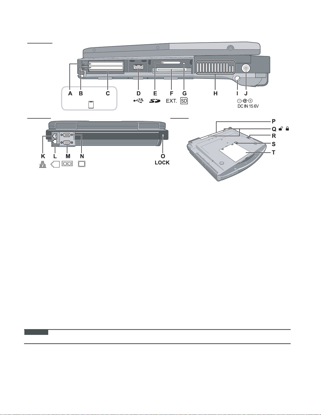
Right side
EX PC
Rear side
A :ExpressCard slot
B :PC Card slot
C :Smart Card slot
<Only for model with Smart Card slot>
D :USB port
E : SD Memory Card slot
F : Expansion bus connector
Bottom
K :LAN port
L : Modem port
M :Serial port
N :External display port
O :Security lock
You can connect a Kensington cable. Refer to the
instruction manual of the cable.
P : Battery pack
Q :Battery latch
R :Multimedia pocket release button
G :SD Memory Card indicator
S : Hard disk drive latch
(Blinking: During access or a password is requested)
T : RAM module slot
H :Ventilation hole
I : Stylus holder
J : DC-IN jack
CAUTION
Do not block the ventilation hole with a thick cloth etc. Select a position with good ventilation.
2-2
Page 11
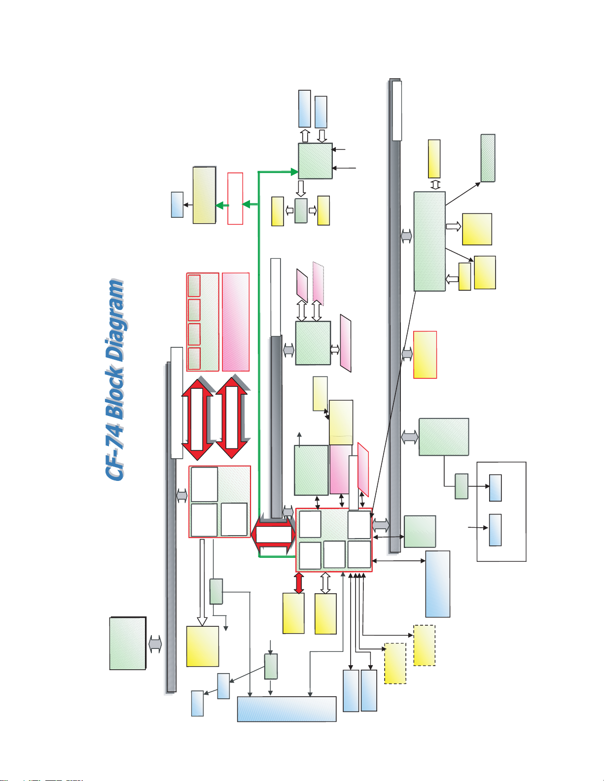
3 Block Diagram
Calistog
a G
LCD
13.3
X
GA
18bit
ICH7-M
Ethe
r
n
et GBe
int
e
3.3V
RJ11
Agere or Conexant
Data Modem
MDC1.5 I/F
in Memory
DDR2 SDRAM
SO-DIMM Ma
SO-DIMM Extension Memory
1.05V AGTL+
64bit BUS 1.8V 667MHz
Processor side Bus 64bit 667MHz
64bit BUS 1.8V 667MHz
3.3V
DDR2 SDRAM
HD Audio
Headphone
Ext. MIC
Sound
STAC9200
AMP
Speaker
SD Card
Smart Card
32bit PCI Bus 33MHz
PCMCIA
R5C811A/812A
antenna
GBE
Speaker
Beep
ODD
TYPE II
Golan 11ABG
Wireless LAN
LPC Bus
PM Signals
EC/KBC
(M306KA)
Module
TPM 1.2
Super I/O
Touch Pad
PC87381
Winbond
Li-Ion
Int. KB
Battey Charger
Pack
Battery
LED
BKLT
Marvell
MiniCard
1.05V
Interface
INTEL
Express Card
PCI Express Bus
LPC
Bridge
USB 2.0
Interface
USB
USB 2.0 x2
USB 2.0 x2
BIOS
Finger Print
25LF080
SPI 8Mbit
Touch screen
Wide Range Wireless
Bluetooth
Buffer
CRT
Serial
CRT
I/O Board
Yukon Ultra
2lane
DMI x2
SATA
SATA HDD
Ethernet GBe
PCI
Bridge
ICH7-M
HDA
Interface
PATA
PATA
IDE
DVD-Combo
Interface
Graphics
nalog 0.7Vpp
A
SW
18bit
(1.05)
INTEL
Calistoga G
Bridge
Host PCI
CRT
Trans
GBE
SW
PR
DRAM
Internal
l
e
int
LVDS 1ch
LCD
RJ45
XGA
”
13.3
3-1
Page 12
4
4.1.
4-1
Page 13
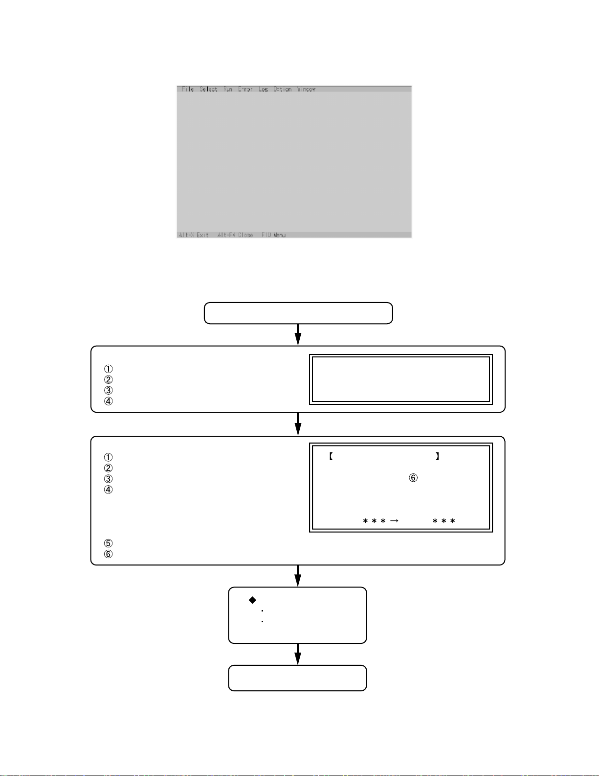
4.2. Troubleshooting
f
k
c
Please take note of the following two points with regard to troubleshooting:
1. Know-how of diagnosis upon occurrence of heavy troubles, e.g. ‘Set cannot be turned ON’, ‘Set fails to start’, ‘No display on
screen’, etc.
2. Explanation of each trouble, mainly symptom of trouble in operation.
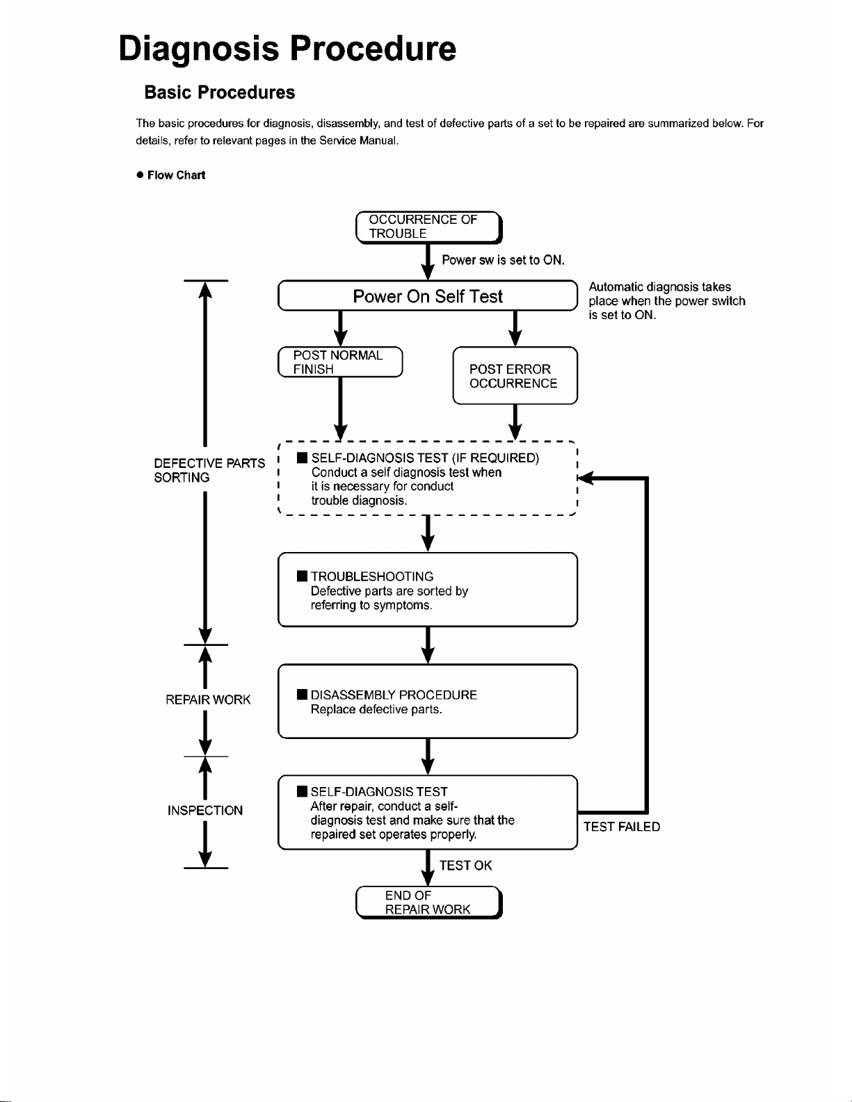
● Flow Chart
START
START
Pay attention to the following points when in pursuit of the cause of a troubleshooting.
1. Peripheral apparatus connected with the set should all be removed before operation check.
2. Make sure that cables, boards, etc. are not coming off, and recheck the contact condition.
Set cannot be supplied with current.
Power lamp fails to light up.
Dark display on screen.
Screen fails to display.
Failure in starting
Return set-up utility setpoint to the state of ‘delivery from factory’.
Not displayed properly on screen.
Some or all keys cannot be input.
Make sure of contact of K/B connector in use.
Replace keyboard or main board.
DVD/CD CALL not practicable.
*Clean DVD-ROM drive with an applicator.
Starts but operates unstably.
Replace DVD drive.
Replace main board.
Reinstall HDD.
Replace main board.
AC
Adaptor/Battery
Output voltage
Power lamp
check
Inverter board
LCD back
light lighting
YES
LCD unit
check
BIOS operation
chec
Result of
POST
Set-up utility
starting
OK
HDD access
YES
Main board
check
OK
Trouble
symptoms on some
of DVD or CD
OK
YES
OK
OK
YES
OK
YES
NO
NG
NO
NG
NO
NG
NG
NO
NG
NG
Replace AC Adaptor/Battery
Check contact condition of power input terminal. Replace i
defective.
Check Power SW. Replace if defective.
Replace inverter board.
Check inverter cable continuity. Replace if defective
Replace LCD back light.
Replace LCD unit.
Replace main board (Check fuse at power source).
Refer to POST
error code table.
Replace main board.
Check HDD cable connection and continuity.
Replace if defective.
Replace HDD & Reinstall.
Replace main board.
Replace main board
Check if there are any flaws on DVD or CD
NO
media. Since flaws may appear on specifi
media, DVD or CD media can be defective.
Replace main board.
Heavy trouble e.g.,
‘Set cannot be turned
ON’, ‘Set fails to start’,
‘No display on
screen’, etc.
Each kind of
trouble in
operation.
START
END
4-2
Page 14
5 Power-On Self Test (Boot Check)
Outline of POST
The set has a boot check function called POST (Power-On Self Test) in it. The condition of the main body is diagnosed by checking
beep sound or error code.
z Start .............Test begins automatically when power switch is set to ON.
z Normal finish .....After memory checking, a beep sound is issued once and the set is placed into automatic stop.
Note: If no error occurs, nothing is displayed. (No display of OK, etc.)
Error Diagnosis by Checking Beep Signal Sound
The beep sound is as follows:
(1 (long sound) -2-3-4)
(Length of bar shows length of sound.)
= long sound (about 0.4 sec.),
z Table of errors classified by beep sounds
Diagnosis Beep signal sound Error message
Main board
(Note) A beep sound is also issued in case of other I/O trouble.
1(long sound)-2 BIOS ROM error
1-2-2-3
1-3-1-1
1-3-1-3
1-3-4-1
1-3-4-3
1-4-1-1
= short sound (about 0.2 sec.), Length between sounds is about 0.1 sec.
BIOS ROM error
RAM error
Keyboard controller error
RAM error
RAM error
RAM error
BIOS ROM error2-1-2-3
Occurrence of unexpected offering2-2-3-1
5-1
Page 15

6 List of Error Codes
<Only when the port replicator is connected>
The following is a list of the messages that BIOS can display. Most of them occur during
POST. Some of them display information about a hardware device, e.g., the amount of memory
installed. Others may indicate a problem with a device, such as the way it has been configured.
Following the list are explanations of the messages and remedies for reported problems.
If your system displays one of except the messages marked below with an asterisk (*), write
down the message and contact Panasonic Technical Support. If your system fails after you
make changes in the Setup menus, reset the computer, enter Setup and install Setup defaults
or correct the error.
0200 Failure Fixed Disk
Fixed disk in not working or not configured properly. Check to see if fixed disk is attached
properly. Run Setup. Find out if the fixed-disk type is correctly identified.
0210 Stuck key
Stuck key on keyboard.
0211 Keyboard error
Keyboard not working.
0212 Keyboard Controller Failed
Keyboard controller failed test. May require replacing keyboard controller.
0213 Keyboard locked - Unlock key switch
Unlock the system to proceed.
0230 System RAM Failed at offset : nnnn
System RAM failed at offset nnnn of in the 64k block at which the error was detected.
0231 Shadow RAM Failed at offset : nnnn
Shadow RAM failed at offset nnnn of the 64k block at which the error was detected.
0232 Extended RAM Failed at offset : nnnn
Extended memory not working or not configured properly at offset nnnn.
0250 System battery is dead - Replace and run SETUP
The CMOS clock battery indicator shows the battery is dead. Replace the battery and run Setup
to reconfigure the system.
*0251 System CMOS checksum bad - Default configuration used
System CMOS has been corrupted or modified incorrectly, perhaps by an application program
that changes data stored in CMOS. The BIOS installed Default SETUP Values. If you do not
want these values, enter Setup and enter your own values. If the error persists, check the system
battery or contact Panasonic Technical Support.
0260 System timer error
The timer test failed. Requires repair of system board.
0270 Real time clock error
Real-time clock fails BIOS test. May require board repair.
*0280 Previous boot incomplete - Default configuration used
Previous POST did not complete successfully. POST loads default values and offers to run
Setup. If the failure was caused by incorrect values and they are not corrected, the next boot
will likely fail. On systems with control of wait states, improper Setup settings can also terminate POST and cause this error on the next boot. Run Setup and verify that the wait-state
configuration is correct. This error is cleared the next time the system is booted.
0281 Memory Size found by POST differed from EISA CMOS
Memory size found by POST differed from EISA CMOS.
6-1
Page 16

02D0 System cache error - Cache disabled
Contact Panasonic Technical Support.
02F0: CPU ID:
CPU socket number for Multi-Processor error.
02F4: EISA CMOS not writable
ServerBIOS2 test error: Cannot write to EISA CMOS.
02F5: DMA Test Failed
ServerBIOS2 test error: Cannot write to extended DMA (Direct Memory Access) registers.
02F6: Software NMI Failed
ServerBIOS2 test error: Cannot generate software NMI (Non-Maskable Interrupt).
02F7: Fail - Safe Timer NMI Failed
ServerBIOS2 test error: Fail-Safe Timer takes too long.
device address Conflict
Address conflict for specified device.
Allocation Error for: device
Run ISA or EISA Configuration Utility to resolve resource conflict for the specified device.
Failing Bits : nnnn
The hex number nnnn is a map of the bits at the RAM address which failed the memory test.
Each 1 (one) in the map indicates a failed bit. See error 230,231 or 232 for offset address of the
failure in System, Extended or Shadow memory.
Invalid System Configuration Data
Problem with NVRAM (CMOS) data.
I/O device IRQ conflict
I/O device IRQ conflict error.
Operating System not found
Operating system cannot be located on either drive A: or drive C:. Enter Setup and see if fixed
disk and drive A: are properly identified.
Parity Check 1 nnnn
Parity error found in the system bus. BIOS attempts to locate the address and display it on the
screen. If it cannot locate the address, it displays ????. Parity is a method for checking errors
in binary data. A parity error indicates that some data has been corrupted.
Parity Check 2 nnnn
Parity error found in the I/O bus. BIOS attempts to locate the address and display it on the
screen. If it cannot locate the address, it displays ????.
Press <F1> to resume, <F2> to Setup
Displayed after any recoverable error message. Press <F1> to start the boot process or <F2> to
enter a Setup and change the settings. Write down and follow the information shown on the
screen.
Troubleshooting
6-2
Page 17

7 Diagnostic Test
Diagnostic Test Procedure
7.1. Equipment
(1)
Test Computer --------------------------------------------------------------------------
(2)
External Floppy Disk Drive (USB Port) ------------------------------------------
(3)
AC Adapter -----------------------------------------------------------------------------
(4)
Loopback Plug (Serial Port Test for RS232C) [P/N: DFWV95C0067] ----
(5)
Floppy Disk containing file DIAG ---------------------------------------------------
7.2. Preparation
(1)
Connect the AC Adapter and External Equipments.
(2)
The System Setup should be set to the factory setting values by executing the "SETUP UTILITY"
which can be invoked by F2 key at the POST.
If not, the messages and items of the diagnostic test may not be displayed properly on the LCD.
(3)
The serial port must be enabled in the "SETUP UTILITY" in order to execute the "1st SERIAL
PORT" test.
(4)
Connect the serial loopback plug.
1 unit
1 unit
-
1 pc.
1 pc.
-
1 pc.
-
7-1
Page 18
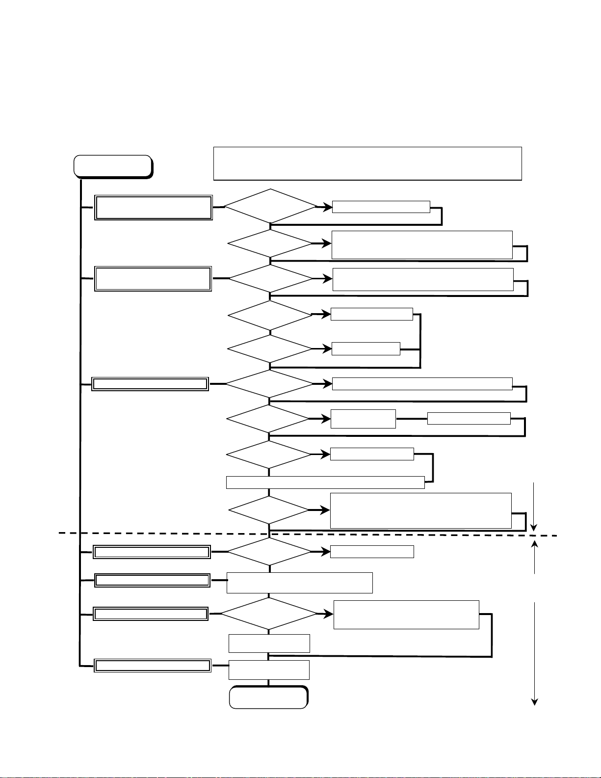
8 Self Diagnosis Test
Floppy disk is Included for the self-diagnostic tests that should be performed before using this product.
Important notice
1. System password
If the password function has been turned on, you will need to ask the user for the password
before performing the self-diagnostics.
2. FDD test
Performing the FDD test will erase the contents of the floppy disk you insert into the drive. Use
a formatted disk that has no contents or whose contents are not required. This product has a
password function. However, if this function is turned on, the self-diagnostics tests will not work.
8.1. Outline of Self Diagnostic Tests
Insert the diagnostics floppy disk
Starting up the setup utility
Turn on the power.
When "Panasonic Press F2 to enter setup" appears
on the screen, press F2.
Return the setup
contents to default
Press " " to select Exit
Press " " to select Get default value
Press Enter.
Choose Yes for "Load default Configuration now?"
Select "Save Values & Exit" and press Enter.
Choose Yes for "Save Configuration changes and exit now?"
and press Enter.
Choose test from
the menu screen
to start the test.
Caution:
After completing repairs, be sure
to carry out the Automatic test
and Peripheraltest.
Menu Screen
1. DIAG on FD (CF-74
2. HDD read Test
3. LAN test
4. SD I/F test
5. Modem I/F test
6. Wireless LAN test (Wireless LAN AB G Model only)
Q. Quit
Select please [ 1, 2, 3, 4, 5, 6, Q ] ?
)
<Automatic test> <Peripheral test> <Test selection>
Tests selected (O) from the test
item list will be performed in
succession.
DIAG on FD
Problems in the unit are located and divided according
to error messages that occur during testing.
The parallel port and CD-ROM
drive can be tested.
(See 8.3 for details.)
2. HDD read Test
3. LAN test
4. SD I/F test
5. Modem I/F test
6. Wireless LAN test
(Wireless LAN AB G Model only)
Specifc tests required can
be freely selected and
performed from the test item
list.
Be sure to carry out the Selection
test only when necessary.
8-1
Page 19
8.1.1 List of main test items
The Selection item displays the items selected under Automatic test. If you select Automatic test, these test items
will be performed automatically. You can use Selection test to choose items from the menu screen that you want to
have tested.
These items are shown below.
1
2
CPU
3
(CPU related)
4
5
RAM (Memory related)
6
CONTROL
7
(Control ICs on the main
8
board, etc.)
9
10
11
12
13
14
15
16
IO
17
(Input-output)
18
COMMUNICATION
19
20
21
AUX
22
(Auxiliary functions)
23
24
VIDEO
25
(Display related)
26
DISK
27
(FDD, HDD)
28
UNIQUE
29
(Individual functions)
30
31
SPEAKER TEST Speaker test
VESA MODE TEST VESA mode test
A20 GATE TEST Address A20 line
CACHE ON/OFF TEST Cache memory on/off test
NPU OPERAND TEST Floating point processor function test
RAM STANDARD TEST Memory standard test
DMA PAGE REG TEST DMA page register test
DMA REGISTER TEST DAM register test
DMAC TRANSFER TEST DAM transfer test
PIC HALT INSTRUCTION TEST Interrupt controller halt instruction test
PIC REGISTER TEST Interrupt controller register test
RTC CMOS RAM TEST Real time clock CMOS test
RTC TEST Real time clock test
PIT CH0 TEST interrupt timer CH0
PIT CH1 TEST interrupt timer CH1
PIT CH2 TEST interrupt timer CH2
KEYBOARD REG TEST Keyboard test
PS/2 MOUSE REG Mouse registration test
SERIAL WRAP TEST Serial loop back (jig required)
SERIAL ALL INTERNAL TEST Serial port interior test
PARALLEL REGISTER R/W Parallel register R/W test
PCIC ALL TEST PCIC test
Card Bus Reg Card Bus register test
USB Reg USB register test
VGA ALL TEST VGA test
SVGA RAM TEST SVGA RAM test
FD WT/RD/WP TEST FD WT, RD WP test
HDD ALL TEST Only HDD lead test selected
ECP REGISTER R/W ECP register R/W test
EPP REGISTER R/W EPP register R/W test
EXT. CMOS R/W TEST Extension CMOS R/W test
Test function settings
8.2. Automatic Test
Test execution
From the menu screen shown below For Celeron models Select and press Enter for DIAG on FD
Test condition save/play
Test automatic execute
Error display (Paging style)
Following file command
Test executed on run settings by selecting command
Select displayed items Error, Log, Option
1. DIAG on FD (CF-74)
2. HDD read Test
3. LAN test
4. SD I/F test
5. Modem I/F test
6. Wireless LAN test (Wireless LAN AB G Model only)
Q. Quit
Select please [ 1, 2, 3, 4, 5, 6, Q ] ?
menu screen
8-2
Page 20
Speaker test, VESA test
The speaker test involves listening to music and choosing OK or Not okay. The VESA test involves looking at
the display to see if it is satisfactory then choosing OK or Not okay.
Serial loop back test
The Automatic test’s initial settings are set so that the serial loop back test will be executed. Connect the serial
loop back jig and then perform the test.
(This test is not executed on default mode)
Diagnostics result
If no errors occur. The screen shows the word "Pass" in large letters.
If errors occur. The test is stopped when an error occurs and the error message is displayed.
For explanations of error messages, see Error Messages and Problem Categories (section 8.5).
Quitting the test
At the screen shown below, simultaneously press the ALT and X keys.
8.3. Peripheral Test
Test execution
From the menu screen shown below, be sure to choose the following items and press Enter.
2. HDD read Test
3. LAN test
4. SD I/F test
5. Modem I/F test
6. Wireless LAN test
(Wireless LAN AB G Model only)
This test checks for internal LAN device.
Choose LAN test and press Enter.
Input screen
1. DIAG on FD (CF-74)
2. HDD read Test
3. LAN test
4. SD I/F test
5. Modem I/F test
6. Wireless LAN test (Wireless LAN AB G Model only)
Q. Quit
Select please [ 1, 2, 3, 4, 5, 6, Q ] ?
menu screen
8-3
Page 21

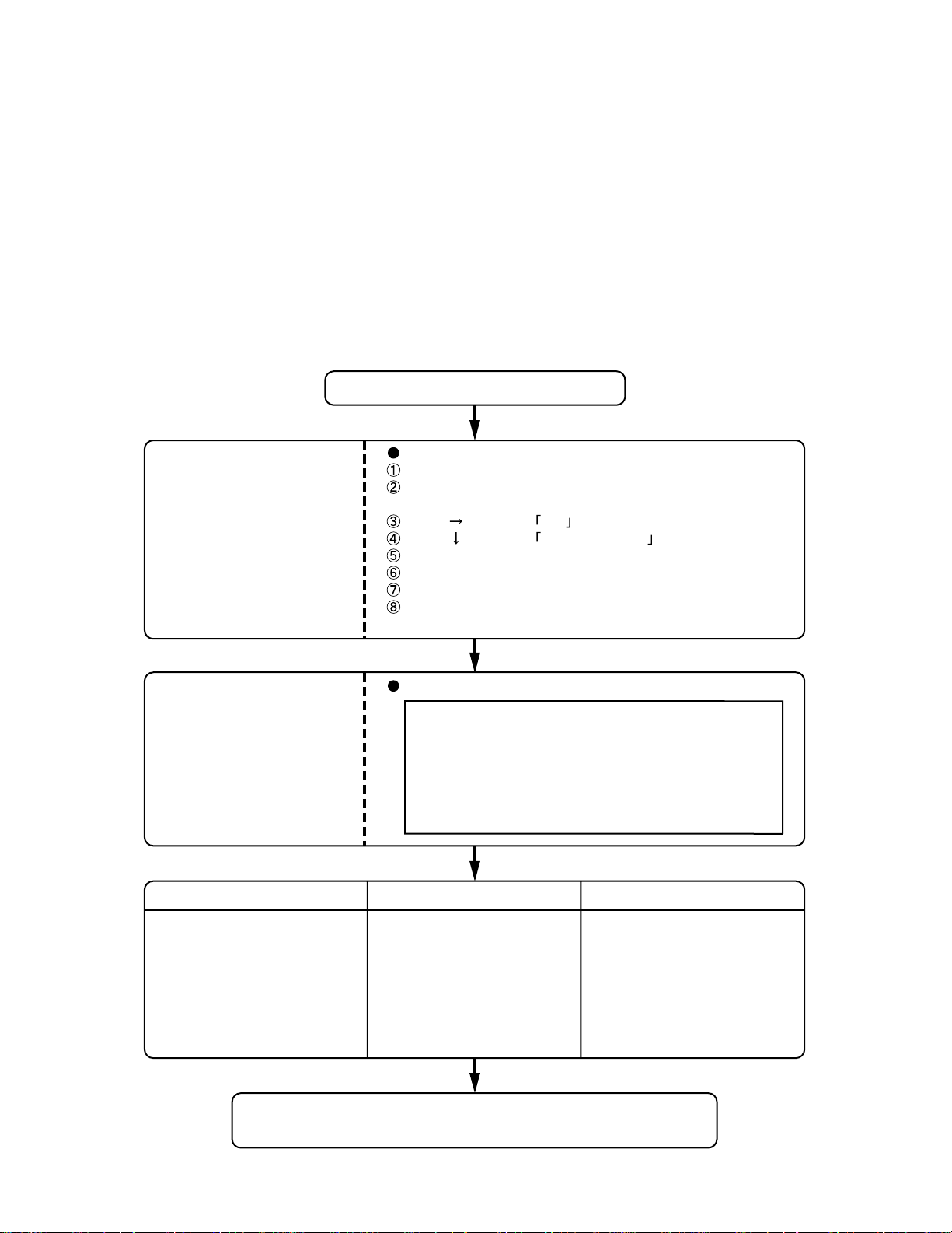
8.4. Test Selection
Starting up the input menu
1. From the menu screen shown below, choose Quit and press Enter.
2. When A: \DIAG appears, input "JDG_74" and press Enter.
3. The input screen shown below will appear.
To choose menu items, hold down "ALT" and press the selection key.
1. DIAG on FD (CF-74)
2. HDD read Test
3. LAN test
4. SD I/F test
5. Modem I/F test
6. Wireless LAN test (Wireless LAN AB G Model only)
Q. Quit
Select please [ 1, 2, 3, 4, 5, 6, Q ] ?
menu screen
8-4
Page 22
Example:
"ALT" + "F" brings up the File menu.
Order of test flow selection
Input screen
Input screen startup
1. Reading the test conditions settings file
Press "AL T" and "F".
Press "L".
Press "AL T" and "C".
2. setting the test items
Press "AL T" and "S".
Press "S".
Choose the test item and press Enter .
Choose the test whose settings are
to be changed, press "A" for Additional
and "R" for Erase.
All initial V Alues are "0" so set
tests other than the necessary ones to "1".
Press "C" twice to return the menu screen.
To save the selected list, press "AL T" and "F" at the file menu.
Starting the test
Press "AL T" and "R".
Press "R".
This will start the test.
If the test condition settings
file is not read, this means
the test program is not running correctly .
Saving selected test items
If you change the file name when
saving the file in step
create test condition settings for
custom test items.
Example:
CF-74 .
, you can
TEST1.
End of test
8-5
Page 23
8.5 . Error Messages and Troubleshooting
The table below explains the parts that may be faulty or damaged should an error message occur while performing the
various test items of the self diagnostics program.
Test classification Screen display test items Contents
1
CPU
2
(CPU related)
3
4 RAM (Memory related)
5
CONTROL
6
(Control ICs on the
7
main board, etc.)
8
9
10
11
12
13
14
15
16
IO
17
(Input-output)
18
COMMUNICATION
19
20
AUX
21
(Auxiliary functions)
22
VIDEO
23
(Display related)
24
25
DISK
26
(FDD, HDD)
27
UNIQUE
28
(Individual functions)
29
A20 GATE TEST Address 20 line
CACHE ON/OFF Cache memory on/off
NPU OPERAND TEST Floating point processor function
RAM STANDARD Memory standard
DMA PAGE REG TEST DMA page register
DMA REGISTER TEST DAM register
DMAC Transfer TEST DAM transfer test
PIC HALT INSTRUCTION TEST Interrupt controller
PIC REGISTER TEST Interrupt controller
RTC CMOS RAM TEST Real time clock CMOS
SPEAKER TEST Speaker
PIT CH0 TEST Interrupt timer CH0
PIT CH1 TEST Interrupt timer CH1
PIT CH2 TEST Interrupt timer CH2
KEYBOARD REG TEST Keyboard
PS/2 MOUSE REG Mouse
SERIAL WRAP TEST Serial loop back (jig required)
SERIAL ALL INTERNAL TEST Serial port
PARALLEL REGISTER R/W Parallel register
PCIC ALL TEST PCIC
Card Bus REG Card Bus port
USB REG USB port
VGA ALL TEST VGA
SVGA RAM TEST SVGA RAM
VESA MODE TEST VESA mode
FD WT/RD/WP TEST FD write/read/write protection
HDD ALL TEST Only HDD lead selected
ECP REGISTER R/W Parallel port
EPP REGISTER R/W Parallel port
EXT. CMOS R/W TEST Extension CMOS R/W test
8-6
Page 24
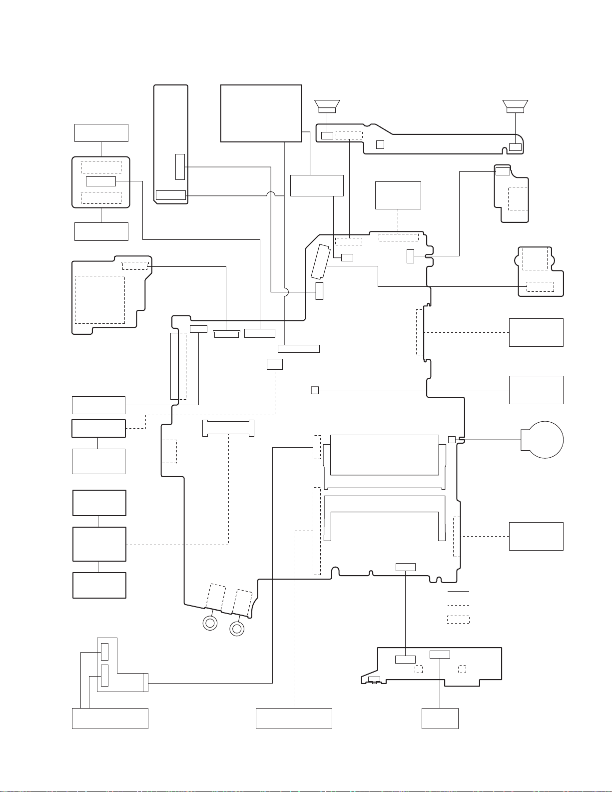
9 Wiring Connection Diagram
I O PCB
SERIAL
CN1203
CN1201
CN1202
VGA
CN1402
SD PCB
TS PCB
CN1401
PORT
REPLICATOR
CN1603
CN23
CN1602
CN6
CN7
LCD
CN24
SPEAKER (R) SPEAKER (L)
SW1001
BATTERY
LED PCB
POWER SW
CN1002
CN1001
CN1003
INVERTER
PAC K
CN17
CN802
CN21
CN19
CN12
CN801
CN18
CN15
CN14
USB PCB
CN1701
USB
CN1702
DC-IN
JK1501
CN1501
DC-IN PCB
DVD-ROM
DRIVE
LAN JACK
MODEM
MODEM
JACK
ANTENNA
PCB L
WIRELESS
MODULE
ANTENNA
PCB R
USB
KBD FPC
CN16
Headphone
JK2
JK1
Microphone
CN5
CN28
MAIN PCB
CN25
CN8
DIMM MEMORY CARD
CN2
CN3
CN26
CN1301
SW1304
SW1301
CN4
CN13
Connector by Cable
Direct connection by Connectors
Parts on Bottom Side
PAD SW PCB
CN1302
SW1303
FAN MOTOR
LITHIUM
BATTERY
HDD PACK
KEYBOARD
PCMCIA SLOT
9-1
FLAT
PAD
Page 25
10 Disassembly/Reassembly
Note:
Power off the computer. Do not shut down to the Suspend or hibernation mode.
Do not add peripherals while the computer is in the Suspend or hibernation mode; abnormal operation may result.
10.1. Disassembly Instructions
10.1.1. Preparation
Before disassembling, be sure to make the following preparations.
• Shut down Windows and turn off the power.
• Disconnect the AC adaptor.
• Remove the optional DIMM memory card and PCMCIA card
if they are connected.
• Remove other devices if they are connected.
Attention:
• Please execute writing BIOS ID when you exchange the
Main Board.
• You cannot reuse the Conductive Clothes and the heat dissipating parts such as Sheet and Rubber. Use new parts.
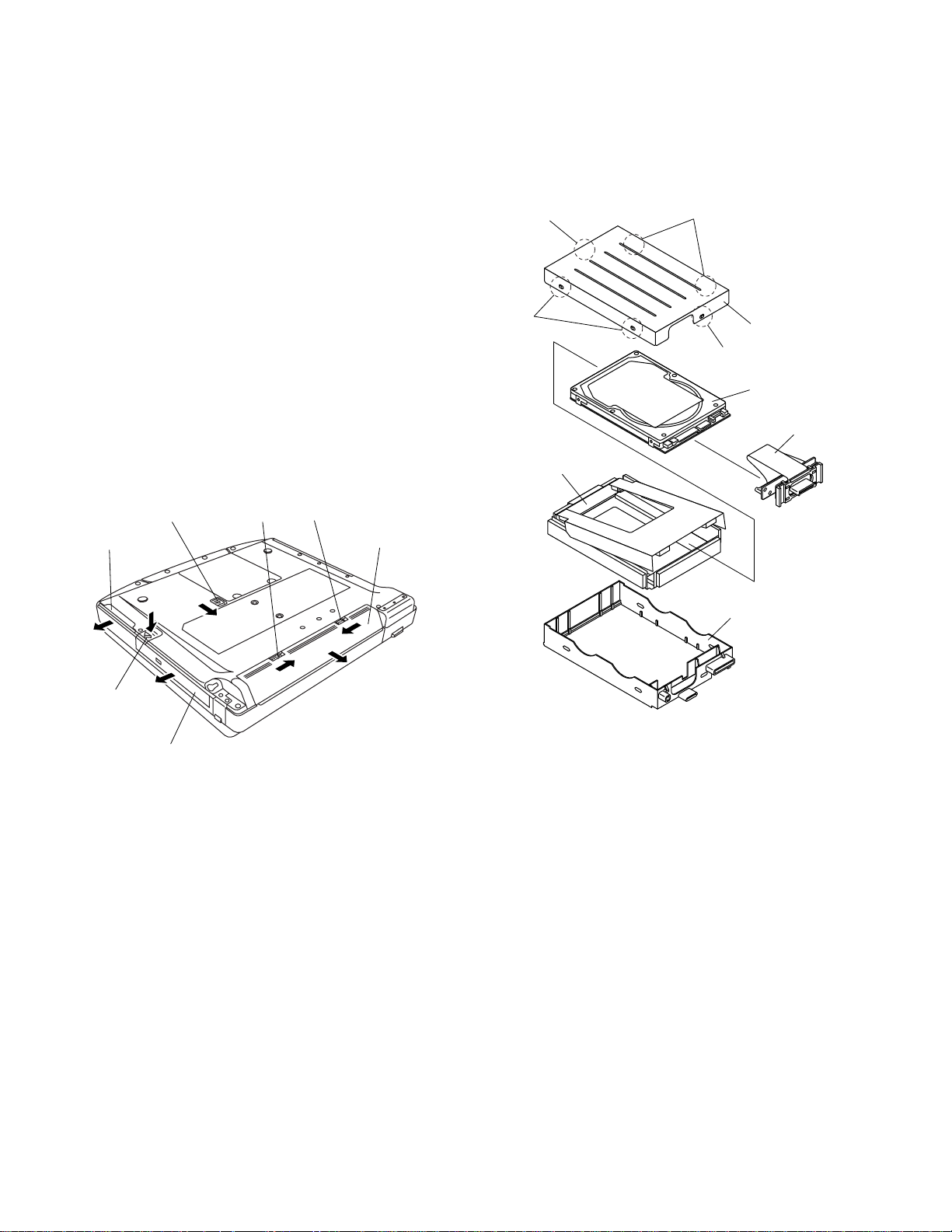
10.1.2. Removing the Battery Pack, the
HDD Unit and the DVD-ROM Drive
Unit
HDD Unit
5
MP Latch
HDD Latch Knob
4
6
7
Latch 2
Latch 1
2
Battery Pack
1
3
10.1.3. Removing the HDD
Hook
Hook
HDD Damper
Hook
HDD Case Upper
Hook
HDD
HDD FPC
HDD Case
DVD-ROM Drive Unit
Battery Pack
1. Slide the Latch 1 to unlock. (1)
2. Slide the Latch 2 (2), and then without releasing it, slide
and remove the Battery Pack. (3)
HDD Unit
1. Slide the HDD Latch Knob (4), and then without releasing
it, slide and remove the HDD Unit. (5)
DVD-ROM Drive Unit
1. Push the MP Latch (6), and then without releasing it, slide
the DVD-ROM Drive Unit. (7)
1. Remove the six Hooks, and remove the HDD Case
Upper.
2. Remove the HDD Damper.
3. Disconnect the HDD from the HDD FPC.
10-1
Page 26

10.1.4. Removing the DIMM Memory Card
<N1>
<N1>
Hook
DIMM Memory Card
DIMM Cover
Hook
2. Lift the upper part of the Center Cover and draw it backward, release the six Hooks fixing the front side of the
Center Cover, and then remove the Center Cover.
3. Remove the four Screws <N9> and the KBD Angle L and
R.
4. Lift the upper part of the Keyboard and draw it backward,
and then turn the Keyboard over forward.
KBD WP Sheet
Connectors
1. Remove the two Screws <N1>, and remove the DIMM
Cover.
2. Open the right and left Hooks of the DIMM Memory Card
outward, and remove the DIMM Memory Card.
Screws <N1>: XSB2+3FNL
10.1.5. Removing the Keyboard
Hooks
1. Release the seven Hooks fixing the rear side of the Center Cover.
Hooks
<N9>
KBD Angle L
Center Cover
Hooks
Keyboard
KBD FPC
Connector
(CN25)
5. Remove the KBD WP Sheet.
6. Disconnect the two KBD Cables from the two Connectors
(KBD FPC).
7. Remove the Keyboard.
8. Disconnect the Cable from the Connector (CN25).
9. Remove the KBD FPC,
Screws <N9>: DFHE5025XA
10.1.6. Removing the Speaker and the LED
PCB
CN1002
Speaker
Holder
Speaker L
Tape
<N9>
CN1003
LED PCB
Tape
Speaker
Holder
Speaker R
Keyboard
<N9>
KBD Angle R
1. Remove the two Speaker Holders.
2. Remove the two tapes, and disconnect the two Speaker
Cables from the two Connectors (CN1002, CN1003)
3. Remove the Speaker L and R.
4. Remove the two Screws <N9>, and Remove the LED
PCB.
Screws <N9>: DFHE5025XA
10-2
Page 27

10.1.7. Removing the Handle Ass'y
<N2>
<N4>
<N4>
Handle Cover L
Handle Cover R
Sleeves A
Sleeves B
10.1.9. Removing the Wireless Module and
MDC Module
<N9>
Antenna Cable (Black)
Antenna Cable (Gray)
Wireless Module
<N9>
Sleeves A
Handle Ass’y
1. Remove the two Screws <N2>.
2. Remove the three Screws <N4>, and remove the Handle
Cover L and R.
3. Remove the two Sleeves A, Handle Ass'y and two
Sleeves B.
Screws <N2>: DRHM4+10FKS
Screws <N4>: DRSB2+6FKL
10.1.8. Removing the Bottom Case
<N7>
<N8>
<N5>
<N7>
<N8>
<N7>
<N7>
<N5>
MDC Module
Modem Cable
1. Remove the two Antenna Cables from the two Connectors.
• Antenna Cable (Black): MAIN Connector
• Antenna Cable (Gray): AUX Connector
2. Remove the two Screws <N9>.
3. Remove the Wireless Module.
4. Remove the two Screws <N9>.
5. Disconnect the Modem Cable from the Connector.
6. Remove the MDC Module.
Screws <N9>: DFHE5025XA
10.1.10. Removing the Main PCB
<N9>
CN6
CN21
CN802
CN18
Bottom Cover
1. Remove the six Screws <N5>.
2. Remove the ten Screws <N7>.
3. Remove the two Screws <N8>.
4. Open the Lid Rubbers and remove the Bottom Cover.
Screws <N5>: DXSB2+6FNL
Screws <N7>: DXYN2+J16FNL
Screws <N8>: DXYN2+J8FNL
10-3
Main PCB
CN26
CN7
CN24
CN28
CN15
<N9>
CN19
MP Guide
Page 28

Note:
After replacing the Main Board, rewrite the BIOS ID.
1. Disconnect the ten Cables from the ten Connectors (CN6,
CN7, CN24, CN19, CN28, CN21, CN802, CN18, CN15,
CN25).
2. Remove the six Screws <N9>.
3. Remove the Main PCB.
4. Remove the MP Guide.
Screws <N9>: DFHE5025XA
1. Remove the two Screws <N9>.
2. Remove the DC-IN PCB.
3. Remove the two Screws <N9>.
4. Remove the four Screws <N19>, and then the I/O PCB
from the I/O Plate.
5. Remove the Modem Cable and LAN Cable from the
MODELAN Holders.
Screws <N9>: DFHE5025XA
Screws <N19>: DFHE5035ZB
10.1.11. Removing the PC Card Ejector and
Lithium Battery
Lithium Battery
(to CN14)
CN14
<N9>
PC Card Ejector
Main PCB
1. Remove the two Screws <N9>.
2. Remove the PC Card Ejector.
3. Disconnect the Cable from the Connector (CN14).
4. Remove the Lithium Battery.
Screws <N9>: DFHE5025XA
10.1.12. Removing the DC-IN PCB and I/O
PCB
MODELAN
Holder
<N9>
<N9>
<N19>
DC-IN PCB
<N9>
Modem Cable
LAN Cable
10.1.13. Removing the FAN Motor and SD
PCB
Cable Holder
Fan Tape1
Fan Duct
<N9>
SD PCB
Heat Sink
Spring
1. Remove the Cable Holder.
2. Remove the two Screws <N5>.
3. Remove the FAN Motor.
4. Remove the Heat Sink, Fan Duct, and the four Heat Sink
Springs.
5. Remove the three Screws <N9>.
6. Remove the SD PCB.
Screws <N5>: DXSB2+6FNL
Screws <N9>: DFHE5025XA
Fan Tape2
<N5>
FAN Motor
Heat Sink
Heat Sink
Spring
MODELAN-2
Holder
I/O PCB
I/O Plate
10-4
Page 29

10.1.14. Removing the USB PCB
10.1.16. Removing the LCD Front Cabinet
<N9>
CN1701
USB PCB
1. Disconnect the Cable from the Connector (CN1701).
2. Remove the two Screws <N9>.
3. Remove the USB PCB.
Screws <N9>: DFHE5025XA
10.1.15. Removing the Display unit
LCD Leg Rubber
<N15>
<N16>
<N15>
LCD Leg
Rubber
LCD Front
Cabinet
LCD Unit
1. Remove the two LCD Leg Rubbers, and then the two
Screws <N16>.
2. Remove the two Screws <N15>.
3. Release the 23 Hooks joining the LCD Front and Rear
Cabinet on the LCD Front Cabinet outward. (See the Figure),
4. Remove the LCD Front Cabinet.
Screws <N15>: DRHM0075ZA
Screws <N16>: DXQT2+G4FCL
<N6>
Hinge
Screw
Cover L
<N6>
Display Unit
<N6>
Hinge
Screw
Cover R
1. Remove the four Screws <N6> from the computer bottom
side.
2. Remove the two Screws <N6> from the computer upper
side.
3. Remove the Display Unit.
4. Remove the Hinge Screw Cover L and R.
Screws. <N6>: DXSB3+6FNL
<N6>
10.1.17. Removing the LCD and the Inverter
LCD Unit
Inverter
Inverter Case
LCD/INV. Cable
<N18>
W-LAN PCB L
<N18>
W-LAN PCB R
LCD Rear Cabinet
10-5
Page 30

1. Disconnect the LCD/INV. Cable from the Connector on
the Inverter.
2. Remove the LCD Unit.
3. Remove the Inverter with the Inverter Case.
4. Remove the two Screws <N18>, and then the W-LAN
PCB L and R.
Screws <N18>: XQN17+BJ6FJ
1. Remove the Palm Rest Sheet.
2. Remove the four Screws <N20>, and then PAD Base
Ass'y.
3. Disconnect the two Cables from the two Connectors
(CN1301, CN1302).
4. Remove the three Screws <N14>.
5. Remove the PAD Button WP Rubber and PAD SW PCB.
6. Remove the Touch PAD.
10.1.18. Removing the Touch PAD and PAD
PCB
Palm Rest Sheet
Pad WP Sheet A
<N20>
<N20>
PAD Base Ass’y
PAD Button
WP Rubber
<N20>
<N20>
Screws <N14>: DRHM0106ZA
Screws <N20>: DXQT2+G4FCL
PAD SW PCB
<N14>
<N14>
Touch PAD
CN1302
CN1301
<N14>
10-6
Page 31

10.2. Reassembly Instructions
10.2.1. Attention when CF-74 series is repaired
• Please execute writing BIOS ID when you exchange the Main Board.
• You cannot reuse the Conductive Clothes and the heat dissipating parts such as Sheet and Rubber. Use new parts.
10.2.2. Setting the LCD Unit and the
Inverter
1. Fix the W-LAN PCB L and R to the LCD Rear Cabinet
using the two Screws <N18>.
2. Attach the Inverter with the Inverter Case to the LCD Rear
Cabinet.
3. Set the LCD Unit to the LCD Rear Cabinet.
4. Connect the LCD/INV. Cable to the Connector on the
Inverter.
Screws <N18>: XQN17+BJ6FJ
Inverter
LCD Unit
Inverter
Case
LCD/INV. Cable
<N18>
W-LAN PCB L
<N18>
W-LAN PCB R
n
n Arranging the W-LAN L and R Cable
nn
Pass the Cable through the notch
and lead it downward.
Lead the Cable along the surface.
Attach the Tape to each of the Cables.
(Avoid overlapping.)
Avoid overlapping of the Cables
(all the way).
Pass the Cable through the notch.
(Avoid running over the ribs.)
LCD Rear Cabnet
LCD Rear Cabinet
W-LAN Antenna L PCB W-LAN Antenna R PCB
Attach the Tape to hold the Cable.
Pass the Cable
through the notch
and lead it downward.
Pass the Cable between
the boss and rib.
Pass the Cable through the notch.
(Avoid running over the ribs.)
10-7
Page 32

n
n Attaching the LCD Damper C and LCD Damper D
nn
1. Attach the four LCD Damper C to the upper part and lower part of the LCD Unit.
2. Attach the LCD Damper D to the upper center of the LCD Unit.
A
LCD Damper D
Match the LCD Damper D to the center
of the LCD Unit.
0~1mm
LCD Unit
A
LCD Display Side
LCD Rear Side
0~1mm
LCD Damper C
LCD Damper C
A: Match the LCD Damper C by LCD edge 0~2mm
n
n Arranging the LCD/TS Cable
nn
1. Connect the LCD/TS Cable (LCD) to the Connector on the LCD Unit.
2. Connect the LCD/TS Cable (TS) to the Connector (CN603) on the TS PCB.
B: Attaching the Cloth
Cushion
Match the end of
the Cloth to the end
of the Cushion.
Cloth
Attach the Cloth along
the surface of
the Cushion.
3~5mm
Cloth
B
Match the end of the Tape to the end of the EMI Sheet.
LCD Unit
TS PCB
LCD/TS Cable
Fold it back and attach to the side surface.
Cloth
Cushion
A
Ensure the Cloth is surely
attached to the metal
chassises on both of the
side and top.
(The Cloth should catch
the metal chassieses only.
It must not catch the TAB.)
Cloth
A
Attach the Cloth
along the surface
of the Cushion.
Cloth
95~100mm
Corner of the Cloth
Ensure the corner of the Cloth
does not come out of the LCD's edge.
Safety Working
A
Safety Working
Turn them halfway.
*Avoid too much tension
on the Cables.
Ensure it does not come out
of the metal part.
Use the Cable covered
with the Conductive Cloth only.
0~2mm
Cloth
Ta pe
Cover the
Connector
Terminals
using the Tape.
EMI Sheet
Before attaching the EMI Sheet,
attach the Tape.
Cloth
B
A: Match the Cloth by Cushion edge 0~1mm
10-8
Page 33

n
n Arranging the TP Power Cable and Attaching the TP/LCD Sheet
nn
Ensure the Tape does not cover the Connecter port.
Safety Working
Match the end of the Sheet
to the end of the Connecter.
Sheet
Connect the Connector.
TP Power Cable
Pass the Cables over
the Conductive Cloth.
Safety Working
Ensure the Tape and Cable Sheet
do not come out of the metal part.
0~1mm
Safety Working
0~2mm
0~2mm
Ta pe
Fold it back and attach
to the side suface.
Safety Working
n
n Setting the Inverter and Arranging the Inverter Cable
nn
Corner of the Conductive Cloth.
No protrusion.
B
A
Arrange the Cable A and B
coming out of the Connector
part in the same length.
Cable Sheet
Safety Working
1. Insert the Inverter to the Inverter Case, and connect the Inverter Cable to the Connector on the Inverter.
2. Fix the Connector of the Inverter Cable using the Tape.
Attach the Inverter on
the two-sided tapes.
Match the end of the Inverter
to the mark.
Ta pe
Safety Working
Pass the Cables through the notch.
Pass the Cable between the LCD and the Inverter Case.
0~1mm
Ta pe
Fold it back and fix it.
Inverter
Case
Inverter Cable
Inverter
1. Avoid any kink, twist or stress on the components.
2. Do not reuse the Inverter once you removed it
from the Inverter Case.
Inverter Case
Safety Working
Match the end of
the Inverter Case
to the end.
Fit the surplus length
under the LCD.
Safety Working
Ensure the portion with
the Black Tape stays on
the outlet.
Ensure the Cables do not
come over the "a" line.
(Otherwise they push up
the front surface.)
"a" line
10-9
Page 34

n
n Cautions for Setting the LCD Unit
nn
Ensure the Cushion does not run
over the rib of the LCD Rear Cabinet.
(Same on the upper side.)
Safety Working
Pull and hold the Cables, and set the LCD.
(Avoid them from being caught inside the LCD unit.)
LCD Unit
LCD Rear Cabinet
Ensure the Cushion does not run over the rib
of the LCD Rear Cabinet.
(Same on the other side.)
10-10
Page 35

10.2.3. Setting the LCD Front Cabinet
1. Set the LCD Front Cabinet to the LCD Rear Cabinet.
2. Fix the LCD Front Cabinet using the two Screws<N15>.
3. Fix the LCD Front Cabinet using the two Screws<N16>,
and attach the two LCD Leg Rubbers.
Screws <N15>: DRHM0075ZA
Screws <N16>: DXQT2+G4FCL
n
n Fixing of the LCD Front Cabinet
nn
Ensure all the 23 Hooks are securely set in.
LCD Leg Rubber
<N16>
: Hooks
<N15>
LCD Front
Cabinet
10.2.4. Setting the Display unit
1. Set the Hinge Screw Cover L and R to the Hinge L and R.
2. Pass the Cables coming out of the LCD Unit into the computer.
3. Fix the Display Unit using the two Screws<N6> from the
computer upper side.
4. Fix the Display Unit using the four Screws<N6> from the
computer bottom side.
Screws. <N6>: DXSB3+6FNL
<N6>
Hinge
Screw
Cover L
<N6>
Display Unit
<N15>
LCD Unit
<N6>
Hinge
Screw
Cover R
<N6>
10-11
Page 36

10.2.5. Setting the USB PCB
1. Fix the USB PCB to the computer using the two
Screws<N9>.
2. Connect the USB Cable to the Connector (CN1701).
Screws <N9>: DFHE5025XA
n
n Arranging the USB Cable
nn
<N9>
CN1701
USB PCB
Safety Working
Connect
the Connector.
Pass it through
the notch.
MP Slide Sheet
Attach the MP Slid Sheet to prevent the Cable from coming off.
USB Cable
Ta pe
Ensure the Cable does not
come out of the board edge
so that the Cable does not
touch the MP Drive.
Avoid runnning over the boss.
MP Slide Sheet
Pass it through
the notch.
Ensure the "A" end does not come on the level.
Fitting edge
A
Pass the Cable through
the notch and lead it downward.
Fit the surplus length of
the Cable into this side.
Fit the Cable between the pins.
Pass it through the rib.
10-12
Page 37

10.2.6. Setting the SD PCB, Heat Sink and FAN Motor
1. Connect the SD FFC to the Connector (CN1401).
2. Fix the SD PCB to the computer using the three
Screws<N9>.
3. Set the Heat Sink, Fan Duct and the four Heat Sink
Springs.
4. Fix the FAN Motor to the computer using the two
Screws<N5>.
5. Attach the Fan Tape 1 and 2 on the FAN Motor, and fix
the Cable Holder on them.
Screws <N5>: DXSB2+6FNL
Screws <N9>: DFHE5025XA
n
n Applying Grease on the Heat Sink
nn
1. Apply grease on two points of the Heat Sink.
2. Attach the Pipe Sheet on the Heat Pipe.
<N9>
SD PCB
Heat Sink
Spring
SD FFC
CN1401
Cable Holder
Fan Tape1
Fan Duct
Fan Tape2
<N5>
FAN Motor
Heat Sink
Heat Sink
Spring
Pipe Sheet
Grease is applied.
G751(10mmX10mmXt0.3)
Match the end of the Pipe Sheet.
(0 ~ -2mm)
Fold on the center line
and attach it.
Fan Dust Sheet
(Attach the Fan Duct Sheet
to the back side.)
5~10mm
Fan Dust Sheet
Heat Sink
Grease is applied.
G751(10mmX10mmXt0.3)
0~1mm
0~1mm
0~1mm
0~1mm
10-13
Page 38

10.2.7. Setting the DC-IN PCB and I/O PCB
1. Fit the Modem Cable and LAN Cable between the MODELAN Holders, and set them on to the computer.
2. Fix the I/O PCB to the I/O Plate using the four
Screws<N19>.
3. Fix the I/O PCB with I/O Plate to the computer using the
two Screws<N9>.
4. Fix the DC-IN PCB to the computer using the two
Screws<N9>.
Screws <N9>: DFHE5025XA
Screws <N19>: DFHE5035ZB
n
n Arranging the DC-IN Cable
nn
DC-IN PCB
<N9>
Modem Cable
MODELAN-2
Holder
LAN Cable
I/O PCB
MODELAN
Holder
<N19>
<N9>
I/O Plate
DC-IN PCB
Safety Working
Fix the Core using the Tape.
Safety Working
Set the Core of the Modem
over the DC-IN Cable.
FAN Cable Sheet
Avoid runnning over the boss.
(Otherwise the Cable will be caught
at the Bottom Cabnet.)
DC-IN Cable
0~3mm
0~3mm
Turn the DC-IN Cable halfway
(counterclockwise)
Attach the Cable avoiding
overlapping
(DC-IN Cable and INV Cable).
Set the INV Cable under
the DC IN Cable.
Connect the Connector
INV. Cable
Safety Working
Fold back the end of Tape.
10-14
Page 39

10.2.8. Setting the PC Card Ejector and Lithium Battery
1. Attach the Lithium Battery to the Main PCB.
2. Pass the Lead Wire of the Lithium Battery through the
groove of the Main PCB, and connect it to the Connector
(CN14) on the back side.
3. Fix the PC Card Ejector to the Main PCB using the two
Screws<N9>.
Lithium Battery
(to CN14)
PC Card Ejector
Screws <N9>: DFHE5025XA
n
n Arranging the Lithium Battery
nn
Safety Working
Pass the Cable through the groove of the Main PCB.
Match the end of the Tape.
(0 to 1 mm)
Tape
CN14
Main PCB
<N9>
Connect to the Connector (CN14) on the back side.
Match the end of the Tape.
(0 to 1 mm)
Fix the Cable using the Tape.
Pass the Cable between the parts.
(Avoid running over the parts.)
Main PCB
10.2.9. Setting the Main PCB
Note:
After replacing the Main Board, rewrite the BIOS ID.
1. Set the MP Guide to the Main PCB.
2. Set the Main PCB to the computer.
3. Fix the Main PCB using the six Screws<N9>.
4. Connect the ten Cables to the corresponding Connecters
(CN6, CN7, CN24, CN19, CN28, CN21, CN802, CN18,
CN15, CN25).
Screws <N9>: DFHE5025XA
Lithium Battery
Main PCB
CN26
CN7
CN24
CN6
<N9>
CN28
CN21
CN802
CN18
CN15
<N9>
CN19
MP Guide
10-15
Page 40

n
n Arranging the Cables to the Cable Holder and their Wiring Order
nn
• Pull the surplus length of the Cable coming from the LCD side to inside of the unit.
(If the surplus length comes outside, it will be caught by the center cover during setting.)
• Fit the Cables to the corresponding grooves of the Cable Holder.
• Ensure the Cables in the Cable Holder are wired in the correct order.
Safety Working
Be sure to wire the Cables in the correct order.
No.1: LAN Cable
No.8: TP Power Cable
No.9: Modem Cable
No.2:
Black Antenna
Cable
No.3:
Gray Antenna
Cable
Fit the portion using the Tape
in the notch.
Fit the Black Tube to the end
of the rib.
No.4: Empty
No.5: I/O Cable
No.6: LCD Cable
n
n Arranging the FAN Cable
nn
FAN Motor
Safety Working
Cover the Cables
using the Tape.
Fold the Tape in half
and attach it to the Cables.
Cable Holder
No.7: LCD Cable with the tube
Safety Working
Lead the FAN Cable into the space next to the Board.
Main PCB
Tape
Fix the FAN Cable.
FAN Cable
Connector (CN28)
Connect the FAN Cable.
10-16
Page 41

10.2.10. Setting the Wireless Module and MDC Module
1. Connect the Modem Cable to the Connector, and fix the
MDC Module to the Main PCB using the two
Screws<N9>.
2. Connect the Wireless Module to the Connector of the
Main PCB, and fix it using the two Screws<N9>.
3. Connect the two Antenna Cables to the two Connectors
on the Wireless Module.
• Antenna Cable (Black): MAIN Connector
• Antenna Cable (Gray): AUX Connector
Wireless Module
<N9>
Antenna Cable (Black)
Antenna Cable (Gray)
Screws <N9>: DFHE5025XA
n
n Arranging the Modem Cable
nn
<Preparation for assembly of the MDC Module>
MDC Module
10–3mm
Fix the Connector
using the Tape.
Fold back and attach to the back side
of the MDC Module.
Safety Working
Ensure the Kapton Tape is
overlapping the Shrink Tube
by 1 mm or more.
Modem Cable
<N9>
MDC Module
Modem Cable
Arranging the Modem Cable
<Good example>
Safety Working
Ensure the Cable does not run over the Screw.
Ensure the Cable does not come over the end
of the MDC Module.
Ensure both of the inlet and outlet
of the Cable are within the frame.
Kapton Tape
Pass the Cable over
the CCC mark.
Avoid any stress on
the outlet of the Cable.
<Bad example>
Coming over the end of the Screw.
Coming over the end
of the Screw.
10-17
Safety Working
Coming outside of the frame.
Page 42

10.2.11. Setting the Bottom Case
1. Set the Bottom Case.
2. Fix the Bottom Case using the ten Screws<N7>. No1 to
No10
3. Fix the Bottom Case using the six Screws<N5>. No11 to
No16
4. Fix the Bottom Case using the two Screws<N8>. No17,
No18
5. Close the Lid Covers.
Note:
Tighten the Screws in the numbered order (No1 to No18).
Screws <N5>: DXSB2+6FNL
Screws <N7>: DXYN2+J16FNL
Screws <N8>: DXYN2+J8FNL
10.2.12. Setting the Handle Ass'y
1. Set the two Sleeves A, the Handle Ass'y and the two
Sleeves B.
2. Fix the Handle Cover L and R using the two Screws<N2>.
No1, No2
3. Fix the Handle Cover L and R using the three
Screws<N4>. No3 to No5
Note:
Tighten the Screws in the numbered order (No1 to No5).
<N7>:No10
<N5>:No12
<N5>:No11
<N5>
:No13
<N5>
:No15
<N7>:No7
Bottom Cover
<N4>
:No5
<N4>
:No4
Handle Cover R
<N7>
:No9
<N7>:No6
<N2>:No2
<N7>:No5
<N8>
:No18
<N5>
:No14
<N7>:No2
<N7>:No1
<N2>:No1
<N7>:No8
<N7>:No4
<N7>:No3
<N5>:No16
<N4>:No3
Handle Cover L
<N8>
:No17
Screws <N2>: DRHM4+10FKS
Screws <N4>: DRSB2+6FKL
Sleeves A
Top Case
Sleeves B
Sleeves A
Handle Ass’y
10-18
Page 43

10.2.13. Setting the Speaker and the LED PCB
1. Fix the LED PCB using the two Screws<N9>.
2. Set the Speaker L and R to the computer.
3. Connect the Speaker Cable L and R to the two Connectors (CN1002, CN1003) on the LED PCB.
4. Fix the Speaker Cable L and R using the Tape.
5. Fix the Speaker L and R using the Speaker Holder.
Note:
Ensure the three Hooks of the Speaker Holder are securely
set in the computer.
Screws <N9>: DFHE5025XA
n
n Soldering the Speaker Cable and Setting the Speaker Rubber
nn
CN1002
Speaker
Holder
Speaker L
Tape
<N9>
CN1003
LED PCB
Tape
Speaker
Holder
Speaker R
Speaker
Soldering
White Line
Red Line
Speaker Cable
n
n Cautions for Setting the Speaker
nn
Safety Working
Speaker L
Ta pe
Speaker
Holder
Soldering
Speaker Rubber
Speaker
Set as the loop of the Speaker Cable
is on the upper side.
Ta pe
Red Line
White Line
SP Conductive
Cloth L
Speaker Cable
Fit to the stand wall.
Fit to
the corner.
SP Conductive
Cloth R
Pass the Speaker Cables
through the notch.
(Avoid running over.)
Ensure the Cable does not
touch the Steel Plate.
Pass the Speaker Cables through the notch.
(Avoid running over.)
Speaker R
10-19
Speaker
Holder
Ensure the Hooks are
securely set in. (3 points)
Speaker L
Securely attach the SP Conductive Cloth
to the round frame of the Speaker.
Speaker R
Page 44

10.2.14. Setting the Keyboard
1. Connect the KBD FPC Cable to the Connector (CN25) of
the Main PCB.
2. Connect the two Cables of the Keyboard to the two Connectors on the KBD FPC.
3. Remove the Release Paper of the KBD WP Sheet, and
attach the KBD WP Sheet to the computer as it covers
the Cable of the Keyboard.
Note:
Press strongly enough until the color of the contact of
two-sided tape is changed.
Connectors
KBD FPC
KBD WP Sheet
Connector
(CN25)
4. Insert the front Hooks of the Keyboard and the FPC to the
computer, and set the Keyboard to the computer.
5. Fix the KBD Angle L and R using the four Screws<N9>.
6. Hook the six front Hooks of the Center Cover to the KBD
Angle L and R.
7. Hook the seven rear Hooks of the Center Cover to the
computer, and press the Center Cover to be securely set
in.
Screws <N9>: DFHE5025XA
n
n Cautions for Setting the Center Cover
nn
Center Cover
Hook with the front hooks.
(six points)
Note:
Do not allow any gaps when
aligning the front hooks.
Center Cover
Hooks
<N9>
KBD Angle L
Keyboard
Push in the claws on the rear side of the dome.
(two each on the left and right)
Push until they are snapped on.
Safety Working
When setting the Center Cover,
fit the Lead Wire in the unit and
avoid it from being caught inside
the dome.
Hooks
<N9>
KBD Angle R
10-20
Ensure the Cable does not
run in this area.
Page 45

10.2.15. Setting the DIMM Memory Card and DIMM Cover
1. Set the DIMM Memory Card to the Main PCB.
2. Fix the DIMM Cover using the two Screws<N1>.
Screws <N1>: XSB2+3FNL
<N1>
Hook
<N1>
DIMM Cover
DIMM Memory Card
10.2.16. Setting the Battery Pack, the HDD Unit and the DVD-ROM Drive Unit
1. Set the DVD-ROM Driver Unit.
2. Set the HDD Pack.
3. Set the Battery Pack.
4. Slide the Latch 1 to the locked position.
Hook
Latch 1
HDD Unit
DVD-ROM Drive Unit
1
Battery Pack
10-21
Page 46

11 Exploded View
E37
K79
B
K80
K75
N20
B
D
K44
N9
N2
K43
K74
B
E27
K64
K65
B
N9
K6
K28
B
N10
A
K27
B
K43
K83
N14
E28
N4
K44
B
K82
A
K29
N20
N14
D
E28
E8
K99
K100
K98
N2
N4
K21
B
K81
K48
N9
K33
K73
E19
K61
K66
K45
K59
K42
E30
K24
B
E31
N6
N5
F
K39
K60
K78
K71
K30
K63
K5
K67
K77
K61
E29
E7
B
N9
E36
K9
B
Screw tightening torque
0.1 ± 0.01 N.m
A
(1.0 ± 0.1 kgf.cm)
E3
K35
K7
N9
K69
K23
E4
K72
F
K62
K46
E32
N6
K37
B
N9
K76
E12
K78
K71
E31
E30
K25
B
N9
K50
K19
B
K41
E34
E35
E5
K38
A
N12
K51
E2
1.2 ± 0.1 N.m
D
(12.0 ± 1.0 kgf.cm)
N9
K40
K68
B
N9
K42
B
B
C
N13
K70
K31
K10
N9
N19
K58
K50
K63
K7
B
N9
K47
N5
B
E33
K1
K32
K39
0.2 ± 0.02 N.m
B
C
(2.0 ± 0.2 kgf.cm)
0.4 ± 0.02 N.m
C
(4.0 ± 0.2 kgf.cm)
0.8 ± 0.1 N.m
F
(8.0 ± 1.0 kgf.cm)
CF-74CCBAXBM
Page 47

E20-1
E17-2
E
N11
E17-3
E21
K55
E17
K53
E20
K56
K54
K17
K52
E13
B
N9
B
B
E1
N9
N9
E38
K49
B
N9
K36
E11
B
N9
K34
K8
N9
B
E
N11
B
N9
E10
N9
B
N9
B
K101
E9
B
N9
K13
B
K85
N9
K95
E
K10
K14
K97
B
N9
A2
E17-4
E17-1
Screw tightening torque
B
0.2 ± 0.02 N.m
(2.0 ± 0.2 kgf.cm)
E
0.13 ± 0.01 N.m
(1.3 ± 0.1 kgf.cm)
E18
B
E17-5
N5
K96
K84
K86
K2
K92
K91
B
N8
B
N9
K89
K87
K95
B
N7
K11
K18
B
N3
K90
B
N7
B
N7
B
N5
B
N5
B
N7
K91
B
K12
N9
B
K88
N8
K93
K94
K20
B
N1
K15
B
N9
K57
CF-74CCBAXBM
Page 48

E14-1
F
N6
E14
K212
K210
K211
K205
K210-6
K210-1
A
N18
K210-2
K26
K16
B
N9
A
N17
E15
K204
E26
E25
B
N16
K204
K201
K208
K207
K3
F
K210-5
K210-3
E15-1
A
N18
K210-4
F
N6
K210-5
F
K4
K207
a
E22
K207
K209
E6
E23
K203
K206
K22
E24
K207
K207
Screw tightening torque
A
0.1 ± 0.01 N.m
(1.0 ± 0.1 kgf.cm)
N15
G
K202
B
0.2 ± 0.02 N.m
(2.0 ± 0.2 kgf.cm)
F
0.8 ± 0.1 N.m
N15
G
(8.0 ± 1.0 kgf.cm)
G
0.375 ± 0.025 N.m
(3.75 ± 0.25 kgf.cm)
CF-74CCBAXBM
Page 49

E22-6-4
E22-2
E22-6-3
E22-4
E22-1
E22-4
E22-5
E22-4
a
E22
E22-4
E22-3
E22-6-5
E22-6-1-1
E22-6-5
E22-6-1
E22-6-6
E22-6-2
E22-6-4
E22-6
CF-74CCBAXBM
Page 50

12 Replacement Parts List
Note: Important Safety Notice
Components identified by mark have special characteristics important for safety.
When replacing any of these components, use only manufacturer's specified parts.
CF-74CCBAXBM
REF.NO. and AREA PART NO. DESCRIPTION Q'TY
Main Block Unit
E1 DL3U11518AAA PCB, MAIN RTL 1
E2 DL3U21518AAA PCB, IO RTL 1
E3 DL3U31518AAA PCB, LED RTL 1
E4 DL3U41518AAA PCB, USB RTL 1
E5 DL3U51518AAA PCB, DC-IN RTL 1
E6 DL3U61518AAA PCB, TS RTL 1
E7 DL3U11501AAA PCB, SD RTL 1
E8 DL3U21501AAA PCB, PAD SWITCH RTL 1
E9 N5ZZ00000090 DIMM 1
E10 N5HAZ0000014 MODEM 1
E11 N5HZC0000019 WIRELESS LAN MODULE 1
E12 DFJS996XA CABLE MODEM ASSY 1
E13 CR2032/S5Y LITHIUM BATTERY 1
E14 DL3UB1514AAA PCB, W-LAN ANTENNA L RTL 1
E14-1 DFJS985ZA CABLE, ANTENNA L (Black) 1
E15 DL3UG1514AAA PCB, W-LAN ANTENNA R
E15-1 DFJS817YA CABLE, ANTENNA R (Gray) 1
E17 DFWV99A0107 HDD MOUNTING KIT 1
E17-1 DL3UP1500AAA FPC, HDD 1
E17-2 DFHM0383ZA HDD CASE UPPER 1
E17-3 DFHR3B92ZA HDD DAMPER 1
E17-4 DFHR6200ZA-0 HDD CASE 1
E17-5 DFHR6203ZA HOLDER HDD CN 1
E18 N3CAYYY00002 HDD 1
E19 DL3UP1499AAA FPC, KBD 1
E20 DFWV78A0243 DRAIVE, DVD-ROM & CD-R/RW 1
E20-1 DFHR9119ZA BEZEL ASSY 1
E21 DL3UP1260BAA FPC, MP DRIVE 1
E22 DFWV08A0081 LCD UNIT ASS'Y 1
E22-1 DL3DE0179AAA LCD UNIT 1
E22-2 DFHR3C55ZA LCD DAMPER A 1
E22-3 DFHR3C56ZA LCD DAMPER B 1
E22-4 DFHR3C57ZA LCD DAMPER C 4
E22-5 DFHR3D14ZA LCD DAMPER D 1
E22-6 DFWV84A0269 TOUCH SCREEN PANEL KIT 1
E22-6-1 DL3DV0179AAA TS PREPARATION UNIT 1
E22-6-1-1 DFHR9068ZA PROTECTIVE FILM 1
E22-6-2 DFHR3243ZA LCD SHEET A 1
E22-6-3 DFHR3244ZA LCD SHEET HDN 1
E22-6-4 DFHR3245ZA LCD SHEET SIDE 2
E22-6-5 DFHR3408ZA TP SHEET 2
E22-6-6 DFMX0778ZA SHEET 1
E23 DFJS998YA CABLE, LCD+TP 1
E24 DFJS993YA CABLE TP POWER 1
E25 N0GF1J000006 INVERTOR 1
E26 DFJS988ZA CABLE INVERTER 1
E27 N2EAYYY00005 TOUCHPAD 1
E28 DFJK12T050DB FFC. PAD 2
E29 DFJK20T040DB FFC, SD 1
E30 L0AA02A00043 SPEAKER 2
RTL 1
Page 51

E31 DFJS991ZA CABLE SPEAKER R 2
E32 DFJS997ZA CABLE_SERIAL 1
E33 UDQFRPH32 FAN 1
E34 DFJS995ZA CABLE LAN ASSY 1
E35 DFJS987ZA CABLE DC IN 1
E36 DFJS992YA CABLE USB 1
E37 N2ABZJ000033 KEYBOARD US 1
E38 K1FY115A0001 PC CARD EJECTOR 1
Accessories
A1 CF-AA1683AM1 AC ADAPTOR 1
A2 N4HUNTA00001 LITHIUM ION BATTERY PACK 1
A3 DFQX5582ZA MANUAL 1
A4 K2CG3DR00003 AC CABLE 1
A5 DFJS954ZA MODEM CABLE 1
A6 DFHS9017ZA TOUCHPANEL FUKINUNO 1
A7 DFHR6207ZA PEN 1
Packing Material
P1 DFPK1182YA PACKING CASE 1
P2 DFPK1185ZA ACCESSORY BOX 1
P3 DFPE0827ZA HOLDER 1
P4 DFPN0834ZA CUSHION T 2
P5 DFPN0835ZA CUSHION B 2
Mechanical Parts
K1 DFUQ0110ZA HEAT SINK SPRING 4
K2 DFMD7A65ZA-0 DIMM COVER 1
K3 DFMD7A83ZA HINGE SCREW COVER L 1
K4 DFMD7A84ZA HINGE SCREW COVER R 1
K5 DFMD9098ZC KENSINGTONG PLATE ASSY 1
K6 DFMC0670YA GASKET 2
K7 DFMX0778ZA INSULATION SHEET 2
K8 DFMX1223ZA INSULATION SHEET JACK 1
K9 DFMY5036ZA ASM HEAT SINK 1
K10 DFHG1446ZA HDD CN CUSHION 1 1
K11 DFHG1815YC-0 IO COVER 1
K12 DFHG1817XB-0 PC CARD COVER 1
K13 DFHG1819ZB-0 USB COVER 1
K14 DFHG1831ZA-0 PEN HOLDER L OUTER 1
K15 DFHG1850ZB-0 COVER 1 1
K16 DFHG1857ZA ANTENNA COVER CUSHION 1
K17 DFHG6034ZB MP GUIDE 1
K18 DFHM0386ZA-0 IO COVER PLATE 1
K19 DFHM0388ZA KBD ANGLE 1
K20 DFHM0390ZA-0 PC COVER PLATE 1
K21 DFHM0395ZB KBD ANGLE L 1
K22 DFHE0494ZA SHEET, LCD FPC 1
K23 DFHE0890ZA DOUDENFU 1
K24 DFHE0991ZA CONDUCTIVE CLOTH SP L 1
K25 DFHE0992ZA CONDUCTIVE CLOTH SP R 1
K26 DFKE0822XA-0 ANT COVER NO ANT 1
K27 DFKE0824ZA-0 HANDLE COVER L 1
K28 DFKE0825ZA-0 HANDLE COVER R 1
K29 DFKE9082ZA-0 HANDLE ASSY 1
K30 DFHR3C29ZA KB WATER PROOF A 1
K31 DFHR3C60ZA FAN CABLE SHEET 1
K32 DFHR3C65ZA SD SHEET 1
K33 DFHR3C70ZA MP SLIDE SHEET TOP 1
K34 DFHR3C91ZA SHEET LED POWER 1
K35 DFHR3D05ZA PWB 5LED SHEET 1
Page 52

K36 DFHR3D06ZA 2FFC INSULATION 1
K37 DFHR3D08ZA ADHESIVE TAPE FAN1 1
K38 DFHR3D10ZA ADHESIVE TAPE FAN2 1
K39 DFHR3D13ZA FAN DUCT SHEET 2
K40 DFHR6204ZA MODELAN-2 1
K41 DFHR6205ZA MODELAN 1
K42 DFHR6211ZA SPEKAER HODLER 2
K43 DFHR6213ZB SLEEVE A 2
K44 DFHR6214ZA SLEEVE B 2
K45 DFHR6221ZA LED LENZ POWER 1
K46 DFHR6234ZB CABLE HOLDER 1
K47 DFHR6235ZA FAN DUCT 1
K48 DFHR6242ZA JACK SPACER 1
K49 DFHR9122ZA HDD GUIDE ASSY 1
K50 DFHG1818ZA-0 SPEAKER RUBBER 2
K51 DFHM0387ZB IO PLATE 1
K52 DFHR3591ZB INSU SHEET CHIP SET 1
K53 DFGT0944YA MP SET LABEL 1
K54 DFKE0709YA-0 MP BOTTOM 1
K55 DFKE0710ZA-0 MP CABINET TOP 1
K56 DFHR6222ZA-0 MP LATCH 1
K57 DFGT1074YA INFORMATION LABEL 1
K58 DFQT9675ZA ENERGY STAR LABEL 1
K59 DFQT9974ZA WINDOWS XP LABEL(NOTE) 1
K60 DFQT9981ZA CENTRINO DUO LABEL 1
K61 DFMC0855ZA USB GASKET 2
K62 DFMC0859ZA FINGER STICK 1
K63 DFHE0513ZA EMI SHEET B 2
K64 DFHE0790ZA USB GASKET 2
K65 DFKM0497ZA-0 TOP CASE 1
K66 DFGL0145YA-0 INDICATOR SHEET B 1
K67 DFGL0146ZA-0 INDICATOR SHEET SD 1
K68 DFGX0438ZA-0 FIN COVER 1
K69 DFGX9023ZB-0 CENTER COVER ASSY 1
K70 DFGX9025YA-0 BT ANT COVER ASSY 1
K71 DFGE0132ZB-0 CENTER COVER NET 2
K72 DFBC0316ZA-0 POWER SW BUTTON 1
K73 DFHR3B96YB-0 PALMREST SHEET 1
K74 DFHR3C30ZA KB WATER PROOF B 1
K75 DFHR3C63ZA MP SLIDE SHEET 1
K76 DFHR3C98ZA KBD WP FIN 1
K77 DFHR3D11ZA PC CARD SHEET 1
K78 DFHR3D43ZA CENTER COVER SPACER 2
K79 DFHR3D48ZA PAD WP SHEET A 1
K80 DFHR3D49ZA PAD WP SHEET B 1
K81 DFHR3D50ZA PAD WP SHEET C 1
K82 DFGX9024YC-0 PAD BASE ASSY 1
K83 DFHR3B95ZA PADBUTTON WP SHEET 1
K84 DFUQ0105ZA LOCK SPRING HDD 1
K85 DFMD7A72ZA SPRING COVER 1
K86 DFMC0855ZA USB GASKET 2
K87 DFMC0859ZA FINGER STICK 1
K88 DFHG1832ZA-0 PEN HOLDER R OUTER 1
K89 DFHG1839ZA-0 LEG LEFT 1
K90 DFHG1840ZA-0 LEG RIGHT 1
K91 DFHG370ZA-1 FOOT RUBBER 2
K92 DFKF0264ZB-0 BOTTOM CASE 1
K93 DFHR3C64ZB NO SMART CARD SHEET 1
Page 53

K94 DFHR3C99ZA NO SC CUSHION 1
K95 DFHR3D15YA PEN FRICTION SHEET 2
K96 DFHR6202ZA-0 HDD LATCH KNOB 1
K97 DFHR6209ZA PEN HOLDER 1
K98 DFHE0997ZA GASKET 1
K99 DFHG1599ZA LCD DUMPER A 1
K100 DFHR3D53ZB SLIDE SHEET 1
K101 DFHR7875ZA PROTECT SHEET, FFC 1
K201 DFMX1209ZA INVERTER CASE 1
K202 DFKF0266ZA-0 LCD FRONT 1
K203 DFHR3599ZA TP/LCD SHEET 1
K204 DFHG1399XA-0 LCD LEG RUBBER 2
K205 DFHR3C84ZA-0 PANASONIC BADGE 1
K206 DFMX0778ZA SHEET 1
K207 DFHE0277ZA GASKET 5
K208 DFHE0418ZA LID MAGNET 1
K209 DFHE0465ZA EMI SHEET 5 1
K210 DFKM9035ZA-0 LCD REAR ASSY 1
K210-1 DFUQ0095ZA LCD LATCH SPRING 1
K210-2 DFDF3147ZA LCD LATCH SHAFT 1
K210-3 DFBH3045ZA HINGE L 1
K210-4 DFBH3046ZA HINGE R 1
K210-5 DXSB3+6FNL SCREW 4
K210-6 DFKE0830ZA-0 LCD LATCH 1
K210-7 DFHR3C49ZA HINGE SCREW COVER 2
K211 DFGX0432ZA-0 ANTENNA COVER C 1
K212 DFGX0433ZA-0 ANTENNA COVER L 1
N1 XSB2+3FNL SCREW 2
N2 DRHM4+10FKS SCREW 2
N3 DRHM5025YA SCREW 3
N4 DRSB2+6FKL SCREW 3
N5 DXSB2+6FNL SCREW 8
N6 DXSB3+6FNL SCREW 6
N7 DXYN2+J16FNL SCREW 10
N8 DXYN2+J8FNL SCREW 2
N9 DFHE5025XA SCREW 43
N10 DRQT2+E8FKL SCREW 2
N11 DFHE5067YA SCREW 2
N12 DXHM0056ZA SCREW 2
N13 DXQT2+E6FNL SCREW 1
N14 DRHM0106ZA SCREW 3
N15 DRHM0075ZA SCREW 2
N16 DXQT2+G4FCL SCREW 2
N17 XQN17+BJ5FJK SCREW 1
N18 XQN17+BJ6FJ SCREW 2
N19 DFHE5035ZB SCREW 4
N20 DXQT2+G4FCL SCREW 4
Page 54

Replacement Parts List
A
Note: Important Safety Notice
Components identified by mark have special characteristics important for safety.
When replacing any of these components use only manufacturer's specified parts.
CF-74CCBAXBM
REF. NO and ARE
MAIN PCB
C 1 F1G1C104A042 CAPACITOR, 16V, 0.1µF 172
C2
C3
C4
C5
C7
C50
C51
C54
C55
C58
C59
C60
C71
C72
C73
C74
C76
C77
C78
C79
C80
C81
C83
C84
C87
C90
C95
C96
C97
C99
C 101
C 103
C 105
C 106
C 116
C 117
C 119
C 120
C 123
C 124
PART NO. DESCRIPTION
Q'TY
Page 55

C 125
C 126
C 149
C 152
C 154
C 156
C 157
C 158
C 161
C 163
C 164
C 165
C 166
C 169
C 170
C 172
C 173
C 174
C 175
C 177
C 178
C 179
C 180
C 181
C 182
C 183
C 184
C 185
C 186
C 187
C 188
C 189
C 190
C 202
C 203
C 204
C 205
C 206
C 207
C 208
C 209
C 212
C 215
C 216
C 217
C 218
C 219
C 220
C 221
C 223
Page 56

C 224
C 225
C 226
C 228
C 229
C 230
C 231
C 234
C 235
C 236
C 237
C 241
C 246
C 247
C 248
C 250
C 251
C 253
C 263
C 266
C 281
C 282
C 286
C 287
C 288
C 291
C 296
C 297
C 298
C 300
C 301
C 304
C 306
C 308
C 309
C 310
C 311
C 314
C 327
C 347
C 349
C 351
C 352
C 353
C 356
C 357
C 358
C 365
C 372
C 373
Page 57

C 389
C 397
C 400
C 401
C 402
C 403
C 406
C 412
C 417
C 428
C 431
C 432
C 433
C 446
C 447
C 450
C 457
C 458
C 459
C 460
C 461
C 462
C 463
C 467
C 817
C 824
C 861
C 892
C 893
C 921
C 922
C 6 EEFUD0D271ER CAPACITOR, 2V, 270µF 2
C 171
C 10 F1J0J4750019 CAPACITOR, 6.3V, 4.7µF 16
C67
C68
C70
C 130
C 135
C 331
C 332
C 333
C 341
C 342
C 343
C 354
C 355
C 376
C 378
C 11 F1J0J226A048 CAPACITOR, 6.3V, 22µF 32
Page 58

C12
C13
C14
C15
C16
C17
C18
C20
C21
C22
C23
C24
C25
C26
C27
C28
C29
C30
C31
C32
C33
C34
C35
C37
C38
C39
C40
C41
C42
C43
C44
C 45 F1J0J106A016 CAPACITOR, 6.3V, 10µF 44
C56
C57
C64
C75
C82
C85
C86
C93
C94
C 102
C 109
C 115
C 118
C 121
C 122
C 162
C 176
C 199
Page 59

C 200
C 201
C 211
C 213
C 243
C 245
C 265
C 269
C 271
C 283
C 307
C 318
C 421
C 422
C 426
C 427
C 804
C 811
C 815
C 818
C 819
C 831
C 845
C 863
C 879
C 46 F1G1H222A496 CAPACITOR, 50V, 2200pF 1
C 61 F1H0J1050022 CAPACITOR, 6.3V, 1µF 24
C63
C65
C66
C69
C91
C92
C98
C 107
C 111
C 112
C 129
C 131
C 136
C 137
C 233
C 315
C 350
C 377
C 396
C 411
C 448
C 449
C 821
Page 60

C 62 EEFCX0D221R CAPACITOR, 2V, 220µF 3
C88
C89
C 155 EEFCX0E221R CAPACITOR, 1
C 108 F1G1A104A014 CAPACITOR, 10V, 0.1µF 18
C 143
C 144
C 145
C 146
C 147
C 148
C 238
C 239
C 319
C 320
C 321
C 322
C 323
C 336
C 348
C 438
C 439
C 110 D4CC1103A038 THERMISTOR 2
C 830
C 127 F1G1H150A542 CAPACITOR, 50V, 15pF 2
C 128
C 132 F1G1E103A062 CAPACITOR, 25V, 0.01µF 33
C 133
C 134
C 138
C 160
C 167
C 191
C 192
C 195
C 196
C 198
C 252
C 274
C 367
C 371
C 374
C 375
C 392
C 407
C 408
C 409
C 419
C 434
C 445
Page 61

C 452
C 808
C 823
C 864
C 888
C 889
C 891
C 920
C 924
C 150 F1H1A1050015 CAPACITOR, 10V, 1µF 24
C 151
C 153
C 159
C 168
C 197
C 214
C 222
C 227
C 242
C 256
C 267
C 268
C 272
C 276
C 277
C 317
C 325
C 326
C 390
C 842
C 865
C 923
C 926
C 193 F1G1H4R0A543 CAPACITOR, 50V, 4pF 3
C 210
C 232
C 194 F1G1H3R00010 CAPACITOR, 50V, 3pF 1
C 244 F1G1C473A004 CAPACITOR, 16V, 0.047µF 1
C 249 F1L3D102A003 CAPACITOR, 2000V, 1000pF 1
C 261 EEFUD0J151ER CAPACITOR, 6.3V, 150µF 1
C 262 F1G1H102A496 CAPACITOR, 50V, 1000pF 20
C 264
C 302
C 303
C 305
C 398
C 399
C 410
C 416
C 418
Page 62

C 424
C 832
C 834
C 844
C 847
C 849
C 851
C 869
C 882
C 917
C 273 F1G1H221A496 CAPACITOR, 50V, 220pF 7
C 275
C 360
C 393
C 394
C 395
C 875
C 285 F1G1H330A542 CAPACITOR, 50V, 33pF 1
C 289 F1J1E105A080 CAPACITOR, 25V, 1µF 4
C 290
C 292
C 293
C 312 F1H1A105A030 CAPACITOR, 10V, 1µF 2
C 440
C 313 F1G1H101A451 CAPACITOR, 50V, 100pF 4
C 430
C 435
C 833
C 324 F1G0J224A001 CAPACITOR, 6.3V, 0.22µF 7
C 328
C 329
C 330
C 335
C 338
C 441
C 361 F1G1H100A544 CAPACITOR, 50V, 10pF 12
C 362
C 363
C 364
C 366
C 368
C 369
C 370
C 846
C 850
C 872
C 878
C 379 F1L1H220A066 CAPACITOR, 50V, 22pF 4
C 380
C 466
Page 63

C 468
C 382 ERJ2RKF1500X RESISTOR, 1/16W, 150Ω 3
C 386
C 388
C 415 F1G1A683A014 CAPACITOR, 10V, 0.068µF 1
C 425 F1G1E472A062 CAPACITOR, 25V, 4700pF 1
C 436 F1G1H471A496 CAPACITOR, 50V, 470pF 2
C 437
C 442 ECJ2FF1A106Z CAPACITOR, 10V, 10µF 2
C 455
C 801 EEFSX0D331ER CAPACITOR, 2V, 330µF 6
C 825
C 826
C 827
C 828
C 829
C 802 F1L1E106A017 CAPACITOR, 25V, 10µF 11
C 803
C 809
C 813
C 814
C 816
C 836
C 867
C 876
C 900
C 932
C 806 F1H1H103A748 CAPACITOR, 50V, 0.01µF 4
C 820
C 868
C 881
C 807 F1H1H104A748 CAPACITOR, 50V, 0.1µF 16
C 838
C 839
C 855
C 856
C 857
C 873
C 874
C 877
C 903
C 906
C 918
C 925
C 928
C 930
C 933
C 810 F1J1E334A081 CAPACITOR, 25V, 0.33µF 2
C 812
C 822 F1H1H562A748 CAPACITOR, 50V, 5600pF 1
Page 64

C 837 F1H1H182A748 CAPACITOR, 50V, 1800pF 2
C 858
C 840 EEFUD0D271ER CAPACITOR, 2V, 270µF 3
C 854
C 859
C 841 EEFCX0J101R CAPACITOR, 6.3V, 100µF 3
C 883
C 884
C 843 F1K1E1060001 CAPACITOR, 25V, 10µF 4
C 853
C 937
C 938
C 860 F1H1H472A748 CAPACITOR, 25V, 4700pF 1
C 862 EEFCD0D101ER CAPACITOR, 2V, 100µF 1
C 866 F1G1H821A496 CAPACITOR, 50V, 820pF 2
C 871
C 870 EEFCX0G151R CAPACITOR, 2V, 150µF 1
C 898 F1G1E223A062 CAPACITOR, 25V, 0.022µF 1
C 904 F1J1E105A009 CAPACITOR, 25V, 1µF 2
C 910
C 927 DCUI1C106HDB CAPACITOR, 16V, 10µF 3
C 931
C 934
C 929 F1G1H152A496 CAPACITOR, 50V, 1500pF 1
CF 1 D4CC1103A038 THERMISTOR 1
CN 2 K1MML0B00003 CONNECTOR 1
CN 3 K1MYL0B00001 CONNECTOR 1
CN 4 K1KA02BA0014 CONNECTOR 1
CN 5 K1MY52B00001 CONNECTOR 1
CN 6 K1KA08BA0014 CONNECTOR 2
CN 21
CN 7 K1MN20BA0134 CONNECTOR 1
CN 8 K1NAF0D00003 CONNECTOR 1
CN 12 K1KB12A00099 CONNECTOR 1
CN 13 K1KY42B00001 CONNECTOR 1
CN 14 K1KA62B00003 CONNECTOR 1
CN 15 K1KA06BA0014 CONNECTOR 1
CN 16 K1FY104BA005 CONNECTOR 1
CN 17 K1KY50AA0103 CONNECTOR 1
CN 18 K1KA05BA0014 CONNECTOR 1
CN 19 K1KB40AA0049 CONNECTOR 1
CN 22 K1MN10BA0070 CONNECTOR 2
CN 27
CN 23 K1FY165EA001 CONNECTOR 1
CN 24 K1KA30BA0060 CONNECTOR 1
CN 25 K1MN30AA0018 CONNECTOR 1
CN 26 K1MY12BA0105 CONNECTOR 1
CN 28 K1KA02BA0085 CONNECTOR 1
CN 801 K1KA10B00213 CONNECTOR 1
CN 802 K1KA06BA0128 CONNECTOR 1
Page 65

D 1 MA2J72900L DIODE 6
D2
D3
D9
D23
D42
D 4 MA3J741E0L DIODE 1
D 10 B0JCPD000023 DIODE 9
D 801
D 804
D 827
D 828
D 829
D 830
D 835
D 836
D 12 B0ADDH000004 DIODE 13
D13
D14
D15
D16
D17
D18
D21
D22
D24
D 837
D 838
D 839
D 19 B0KB00000044 DIODE 3
D20
D34
D 33 MA2S111-TX DIODE 4
D 821
D 823
D 824
D 38 B3ABB0000210 DIODE 1
D 39 B3AGB0000040 DIODE 1
D 40 B3ADB0000065 DIODE 1
D 802 B0JCCE000008 DIODE 2
D 803
D 805 B0ADCJ000025 DIODE 3
D 808
D 811
D 806 B0JCMD000014 DIODE 6
D 807
D 809
D 810
D 812
D 840
Page 66

D 813 MAZ80620ML DIODE 6
D 815
D 816
D 817
D 818
D 819
D 820 B2ABAM000002 DIODE 1
D 825 MAZ81800ML DIODE 1
D 826 MAZ81200ML DIODE 1
D 831 B0JDBE000002 DIODE 3
D 833
D 834
D 832 B0JDRE000007 DIODE 1
F 1 K5H202Z00005 FUSE, 2A 5
F2
F4
F5
F9
F 3 K5H402Z00003 FUSE, 4A 1
IC 1 C2GBC0000283 IC, CPU 1
IC 2 C0JBZZ000387 IC, TEMPERATURE CENSOR 1
IC 3 C1CB00002360 IC, CHIPSET 1
IC 4 C0DBZYY00017 IC 1
IC 6 C0JBZZ000388 IC, CLOCK GENERATOR 1
IC 7 C0JBAB000619 IC, GATE LOGIC 1
IC 8 C1DB00001541 IC, CHIPSET 1
IC 9 C0JBAA000344 IC, GATE LOGIC 6
IC 32
IC 42
IC 63
IC 71
IC 801
IC 10 C1DB00001362 IC, LSI 1
IC 11 C3EBFY000003 IC, EPROM 1
IC 12 C0DBEFE00003 IC 1
IC 13 C0JBAZ002420 IC, LAN SW 1
IC 15 C1CB00002279 IC 1
IC 16 C0DBZYY00016 IC 1
IC 17 C1CB00002278 IC, SUPER I/O 1
IC 18 C0ZBZ0000978 IC 1
IC 20 C3FBLY000009 IC, FLASH ROM 1
IC 21 C1CB00002268 IC, SECURITY CHIP 1
IC 22 C0CBCBC00137 IC, REGURATOR 1
IC 23 C2CBJA000003 IC, MICON 1
IC 25 C1CB00002449 IC, AUDIO CODEC 1
IC 26 C1AB00002507 IC, AUDIO POWER AMPLIFIER 1
IC 27 C0JBZZ000383 IC 2
IC 28
IC 29 C0DBZYY00026 IC, USB POWER SW 3
IC 46
Page 67

IC 74
IC 30 C0JBAB000624 IC 2
IC 58
IC 33 C0JBAE000302 IC, LOGIC IC 1
IC 35 C0JBAB000616 IC, LOGIC IC 2
IC 812
IC 36 C0JBAR000500 IC, SWITCH 1
IC 37 C0JBAA000431 IC 1
IC 39 C0EBE0000459 IC 3
IC 40
IC 44
IC 47 C0JBAA000340 IC, GATE LOGIC 1
IC 51 C0CBCBC00181 IC 1
IC 56 C1CB00002295 IC 1
IC 57 C0DBZYY00019 IC, POWER MANAGEMENT SWITCH 1
IC 60 C0ABBA000093 IC, OP AMP 2
IC 817
IC 72 C0JBAZ002422 IC, FET SWITCH 2
IC 73
IC 802 C0DBZYY00013 IC, FET 2
IC 803
IC 804 C0DBAYY00051 IC 1
IC 805 C0DBALH00003 IC 3
IC 807
IC 809
IC 806 C0DBEZG00024 IC 1
IC 808 C0DBEFH00002 IC, REGULATOR 1
IC 810 C0EBE0000333 IC 1
IC 811 C0JBAD000182 IC, LOGIC IC 1
IC 813 C0EBH0000336 IC 2
IC 814
IC 815 C0ABZA000047 IC, AMP 1
IC 818 C0DBDJH00009 IC, LINEAR 1
JK 1 K2HC103B0197 JK 2
JK 2
L 1 G1C1R0MA0076 INDUCTOR 2
L4
L 2 G1C91NM00001 INDUCTOR 1
L 3 J0JJC0000021 INDUCTOR 8
L5
L7
L11
L22
L23
L35
L36
L 8 J0MAB0000169 INDUCTOR 2
L9
L 10 J0JDC0000045 INDUCTOR 15
L13
Page 68

L14
L15
L16
L17
L18
L19
L24
L25
L30
L31
L32
L33
L43
L 12 J0MAB0000200 INDUCTOR 6
L20
L21
L34
L44
L45
L 37 DDB5Z021C-Y INDUCTOR 6
L38
L39
L40
L41
L42
L 801 G1AR56PA0001 INDUCTOR 2
L 802
L 803 G1C2R8MA0022 INDUCTOR 1
L 804 G1C4R7MA0022 INDUCTOR 3
L 805
L 807
L 806 DDAZS100MT3T INDUCTOR 1
L 808 J0JKC0000007 INDUCTOR 2
L 809
L 810 G1A160H00001 INDUCTOR 1
PA 1 K5J1BB000001 POLY SW 3
PA 2
PA 3
Q 4 2SB0766ARL TRANSISTOR 1
Q 9 B1GBCFNN0042 TRANSISTOR 27
Q22
Q23
Q24
Q45
Q58
Q82
Q 810
Q 817
Q 824
Q 827
Page 69

Q 830
Q 832
Q 833
Q 834
Q 836
Q 837
Q 838
Q 852
Q 858
Q 859
Q 870
Q 871
Q 872
Q 873
Q 879
Q 880
Q 12 B1GBCFJN0037 TRANSISTOR 10
Q 844
Q 846
Q 851
Q 854
Q 855
Q 856
Q 857
Q 862
Q 868
Q 13 B1GFCFNN0019 TRANSISTOR 6
Q69
Q70
Q72
Q 869
Q 874
Q 19 XP0421300L TRANSISTOR 3
Q21
Q78
Q 20 B1MBDCA00004 TRANSISTOR 8
Q43
Q46
Q56
Q71
Q73
Q75
Q77
Q 25 B1CFGD000023 TRANSISTOR 18
Q47
Q48
Q67
Q76
Q80
Q81
Page 70

Q 803
Q 809
Q 815
Q 816
Q 819
Q 825
Q 826
Q 865
Q 866
Q 867
Q 881
Q 27 B1DHDC000028 TRANSISTOR 2
Q57
Q 28 XP0411500L TRANSISTOR 7
Q29
Q30
Q31
Q32
Q33
Q34
Q 79 B1GDCFNN0031 TRANSISTOR 8
Q 804
Q 829
Q 845
Q 847
Q 853
Q 860
Q 861
Q 801 B1CFRD000009 TRANSISTOR 2
Q 807
Q 802 B1DFGD000032 TRANSISTOR 4
Q 805
Q 806
Q 808
Q 811 B1DBGD000006 TRANSISTOR 9
Q 812
Q 814
Q 818
Q 822
Q 823
Q 841
Q 842
Q 884
Q 813 B1MBEDA00017 TRANSISTOR 3
Q 821
Q 828
Q 849 B1CHRD000001 TRANSISTOR 6
Q 875
Q 876
Q 877
Page 71

Q 878
Q 882
Q 850 B1GFCFJN0016 TRANSISTOR 2
Q 885
Q 863 B1DDDC000003 TRANSISTOR 2
Q 864
Q 883 B1DHFD000015 TRANSISTOR 1
R 2 ERJ2GEJ102X RESISTOR, 1/16W, 1KΩ 13
R63
R66
R67
R 111
R 156
R 159
R 227
R 228
R 330
R 337
R 406
R 434
R 3 ERJ2RKF1500X RESISTOR, 1/16W, 150Ω 4
R51
R52
R53
R 6 ERJ2RKF1000X RESISTOR, 1/16W, 100Ω 5
R7
R26
R28
R32
R 8 ERJ2RKF27R4X RESISTOR, 1/16W, 27.4Ω 2
R9
R 10 ERJ2RKF54R9X RESISTOR, 1/16W, 54.9Ω 4
R11
R34
R35
R 12 ERJ2RKF2001X RESISTOR, 1/16W, 2KΩ 1
R 13 ERJ2RKF1001X RESISTOR, 1/16W, 1KΩ 2
R 806
R 15 ERJ2RKF51R0X RESISTOR, 1/16W, 51Ω 1
R 17 D1H85104A024 RESISTOR ARRAY 1
R 18 ERJ2GEJ100X RESISTOR, 1/16W, 10Ω 13
R93
R 429
R 829
R 830
R 843
R 844
R 849
R 850
R 865
Page 72

R 870
R 872
R 877
R 19 ERJ2GEJ562X RESISTOR, 1/16W, 5.6KΩ 5
R 916
R 925
R 927
R 968
R 20 ERJ2GEJ560X RESISTOR, 1/16W, 56Ω 2
R24
R 21 ERJ2GEJ240X RESISTOR, 1/16W, 24Ω 1
R 22 ERJ2RKF75R0X RESISTOR, 1/16W, 75Ω 1
R 25 ERJ2RKF68R0X RESISTOR, 1/16W, 68Ω 2
R 218
R 27 ERJ2RKF2210X RESISTOR, 1/16W, 221Ω 2
R29
R 30 ERJ2RKF24R9X RESISTOR, 1/16W, 24.9Ω 5
R31
R55
R 145
R 162
R 33 ERJ2RKF2000X RESISTOR, 1/16W, 200Ω 1
R 38 ERJ2RKF80R6X RESISTOR, 1/16W, 80.6Ω 2
R39
R 47 ERJ2GEJ101X RESISTOR, 1/16W, 100Ω 22
R 106
R 121
R 130
R 182
R 198
R 215
R 274
R 314
R 368
R 374
R 382
R 430
R 439
R 894
R 895
R 896
R 897
R 898
R 899
R 957
R 961
R 48 ERJ2GEJ330X RESISTOR, 1/16W, 33Ω 14
R49
R 107
R 211
Page 73

R 248
R 310
R 317
R 364
R 365
R 404
R 411
R 412
R 413
R 414
R 50 ERJ2RKF2550X RESISTOR, 1/16W, 255Ω 1
R 54 ERJ2RKF1501X RESISTOR, 1/16W, 1.5KΩ 1
R 57 ERJ2RKF1002X RESISTOR, 1/16W, 10KΩ 6
R 285
R 835
R 840
R 841
R 876
R 61 D1H81034A024 RESISTOR ARRAY 12
R94
R 101
R 135
R 144
R 157
R 239
R 245
R 327
R 415
R 428
R 441
R 72 ERJ2GEJ220X RESISTOR, 1/16W, 22Ω 2
R 238
R 73 ERJ2GEJ103X RESISTOR, 1/16W, 10KΩ 52
R88
R 103
R 108
R 137
R 140
R 161
R 240
R 242
R 243
R 247
R 251
R 259
R 263
R 266
R 271
R 273
R 277
Page 74

R 291
R 295
R 297
R 312
R 324
R 326
R 328
R 329
R 332
R 333
R 339
R 354
R 369
R 375
R 386
R 400
R 407
R 409
R 436
R 437
R 438
R 440
R 804
R 805
R 809
R 826
R 827
R 831
R 847
R 863
R 920
R 947
R 948
R 972
R 80 D1H85604A024 RESISTOR ARRAY 2
R84
R 81 D1HA56080001 RESISTOR ARRAY 6
R82
R83
R85
R86
R87
R 91 ERJ2GE0R00X RESISTOR, 1/16W, 0Ω 36
R 134
R 136
R 147
R 163
R 172
R 176
R 202
Page 75

R 205
R 210
R 220
R 222
R 223
R 225
R 226
R 234
R 256
R 260
R 268
R 269
R 276
R 281
R 345
R 419
R 422
R 424
R 435
R 445
R 446
R 801
R 818
R 838
R 929
R 934
R 960
R 983
R 95 ERJ2GEJ1R0X RESISTOR, 1/16W, 1Ω 6
R96
R 158
R 308
R 384
R 385
R 97 DEARA8CJ330M RESISTOR ARRAY 1
R 104 ERJ2GEJ104X RESISTOR, 1/16W, 100KΩ 36
R 105
R 110
R 138
R 139
R 155
R 170
R 171
R 174
R 214
R 221
R 224
R 230
R 231
R 232
Page 76

R 237
R 278
R 338
R 340
R 341
R 353
R 355
R 358
R 359
R 360
R 366
R 367
R 431
R 432
R 433
R 449
R 836
R 859
R 917
R 918
R 950
R 109 D1H84724A024 RESISTOR ARRAY 2
R 141
R 298 D1H84734A024 RESISTOR ARRAY 2
R 334
R 131 ERJ2RKF22R6X RESISTOR, 1/16W, 22.6Ω 1
R 133 ERJ2GEJ471X RESISTOR, 1/16W, 470Ω 4
R 342
R 343
R 401
R 148 ERJ2GEJ470X RESISTOR, 1/16W, 47Ω 2
R 421
R 149 DEARA8AJ103M RESISTOR ARRAY 2
R 179
R 154 ERJ2GEJ121X RESISTOR, 1/16W, 120Ω 1
R 160 ERJ2GEJ106X RESISTOR, 1/16W, 10MΩ 1
R 164 ERJ2GEJ472X RESISTOR, 1/16W, 4.7KΩ 15
R 199
R 200
R 201
R 292
R 313
R 371
R 372
R 443
R 444
R 447
R 448
R 944
R 945
Page 77

R 976
R 167 ERJ2GEJ203X RESISTOR, 1/16W, 20KΩ 1
R 168 ERJ2GEJ105X RESISTOR, 1/16W, 1MΩ 10
R 196
R 377
R 378
R 888
R 889
R 890
R 891
R 893
R 906
R 173 D1HG2208A001 RESISTOR ARRAY 1
R 178 D1H81004A024 RESISTOR ARRAY 1
R 180 DEARA8AJ103M RESISTOR ARRAY 6
R 181
R 279
R 284
R 287
R 403
R 188 ERJ2RKF49R9X RESISTOR, 1/16W, 49.9Ω 8
R 189
R 190
R 191
R 192
R 193
R 194
R 195
R 203 ERJ2RKF4871X RESISTOR, 1/16W, 4.87KΩ 1
R 206 ERJ2RHD103X RESISTOR, 1/16W, 10KΩ 4
R 209
R 282
R 955
R 208 ERJ2RHD303X RESISTOR, 1/16W, 30KΩ 1
R 212 ERJ2GEJ473X RESISTOR, 1/16W, 47KΩ 13
R 229
R 304
R 325
R 361
R 376
R 883
R 903
R 922
R 928
R 930
R 935
R 942
R 213 D1H87504A024 RESISTOR ARRAY 1
R 236 ERJ2GEJ273X RESISTOR, 1/16W, 27KΩ 1
R 272 ERJ2RKF3901X RESISTOR, 1/16W, 3.9KΩ 2
Page 78

R 275
R 289 ERJ6GEY0R00V RESISTOR, 1/10W, 0Ω 1
R 294 ERJ2GEJ223X RESISTOR, 1/16W, 22KΩ 6
R 296
R 301
R 303
R 864
R 904
R 299 ERJ2GEJ333X RESISTOR, 1/16W, 33KΩ 4
R 845
R 846
R 874
R 300 ERJ2GEJ153X RESISTOR, 1/16W, 15KΩ 5
R 302
R 828
R 848
R 866
R 306 ERJ2GEJ390X RESISTOR, 1/16W, 39Ω 2
R 307
R 309 ERJ2RKF5101X RESISTOR, 1/16W, 5.1KΩ 2
R 807
R 331 ERJ2GEJ474X RESISTOR, 1/16W, 470KΩ 5
R 882
R 926
R 932
R 975
R 336 D1H81014A024 RESISTOR ARRAY 1
R 344 ERJ2GEJ181X RESISTOR, 1/16W, 180Ω 4
R 346
R 352
R 442
R 347 D1HG2218A001 RESISTOR ARRAY 1
R 348 ERJ2GEJ221X RESISTOR, 1/16W, 220Ω 3
R 349
R 861
R 370 ERJ2GEJ222X RESISTOR, 1/16W, 2.2KΩ 5
R 373
R 379
R 380
R 408
R 417 ERJ2GEJ334X RESISTOR, 1/16W, 330KΩ 1
R 802 ERJ2RKF1821X RESISTOR, 1/16W, 1.82KΩ 1
R 803 D1JB1M00A001 RESISTOR, 1W, 1mΩ 2
R 811
R 808 ERJ2RKF1020X RESISTOR, 1/16W, 102Ω 3
R 810
R 816
R 812 ERJ2RKF2050X RESISTOR, 1/16W, 205Ω 1
R 813 ERJ2RKF6980X RESISTOR, 1/16W, 698Ω 1
R 814 ERJ2RKF3400X RESISTOR, 1/16W, 340Ω 1
Page 79

R 815 ERJ2RKF2490X RESISTOR, 1/16W, 249Ω 1
R 817 ERJ2RHD561X RESISTOR, 1/16W, 560Ω 1
R 819 ERJ3GEYJ100V RESISTOR, 1/16W, 10Ω 4
R 842
R 862
R 887
R 820 ERJ3GEYJ3R3V RESISTOR, 1/16W, 3.3Ω 4
R 821
R 822
R 823
R 824 ERJ3GEY0R00V RESISTOR, 1/16W, 0Ω 3
R 825
R 967
R 832 D1BDR0220001 RESISTOR, 1/8W, 0.022Ω 10
R 833
R 839
R 852
R 857
R 858
R 869
R 873
R 875
R 879
R 834 ERJ2RKF3161X RESISTOR, 1/16W, 3.16KΩ 1
R 851 D1BDR0330001 RESISTOR, 1/8W, 0.033Ω 4
R 860
R 867
R 977
R 853 ERJ2RKF1802X RESISTOR, 1/16W, 18KΩ 1
R 854 ERJ2RKF1602X RESISTOR, 1/16W, 16KΩ 1
R 855 ERJ2RHD2552X RESISTOR, 1/16W, 25.5KΩ 1
R 856 ERJ2RHD203X RESISTOR, 1/16W, 20KΩ 1
R 868 ERJ2RKF6201X RESISTOR, 1/16W, 6.2KΩ 1
R 871 ERJ2RKF3002X RESISTOR, 1/16W, 30KΩ 1
R 878 ERJ2RKF2002X RESISTOR, 1/16W, 20KΩ 1
R 880 ERJ2RKF1003X RESISTOR, 1/16W, 100KΩ 3
R 937
R 941
R 881 ERJ2RKF1301X RESISTOR, 1/16W, 1.3KΩ 1
R 884 ERJ2RKF1302X RESISTOR, 1/16W, 13KΩ 1
R 885 ERJ2RKF5601X RESISTOR, 1/16W, 5.6KΩ 2
R 886
R 901 ERJ6GEYJ222V RESISTOR, 1/16W, 2.2KΩ 2
R 902
R 919 D1BDR4700001 RESISTOR, 1/8W, 0.47Ω 1
R 921 ERJ2GEJ3R3X RESISTOR, 1/16W, 3.3Ω 2
R 933
R 923 ERJ2GEJ564X RESISTOR, 1/16W, 560KΩ 4
R 931
R 943
Page 80

R 946
R 936 ERJ2RKF4702X RESISTOR, 1/16W, 47KΩ 2
R 940
R 938 ERJ2RKF3302X RESISTOR, 1/16W, 33KΩ 2
R 939
R 952 ERJ2RHD153X RESISTOR, 1/16W, 15KΩ 1
R 954 ERJ2RHD104X RESISTOR, 1/16W, 100KΩ 2
R 956
R 953 D1JB4M00A001 RESISTOR, 1W, 4mΩ 1
R 958 ERJ2RKD154X RESISTOR, 1/16W, 150KΩ 2
R 959
R 962 D1BDR1000002 RESISTOR, 1/8W, 0.1Ω 6
R 963
R 964
R 978
R 981
R 985
R 965 ERJ2RKF1503X RESISTOR, 1/16W, 150KΩ 1
R 966 ERJ2RKF3652X RESISTOR, 1/16W, 36.5KΩ 1
R 969 ERA3EEB1692V RESISTOR, 1/16W, 16.9KΩ 1
R 970 ERJ2RKF3001X RESISTOR, 1/16W, 3KΩ 2
R 973
R 971 ERJ2RKF1103X RESISTOR, 1/16W, 110KΩ 1
R 984 ERA3EKB1623V RESISTOR, 1/16W, 162KΩ 1
T 1 G5BYC0000015 TRANCE 2
T2
X 1 H0J143500058 OSCILLATOR, 14.3MHz 1
X 2 H0J327200115 OSCILLATOR, 32.768KHz 1
X 3 H0J250500067 OSCILLATOR, 25MHz 1
X 4 H2D800400015 OSCILLATOR, 8MHz 1
ZA 1 DRHM0100ZA SCREW 2
ZA 2
ZA 3 K1YGZZ000055 NUT 2
ZA 4
IO PCB
C 1204 F1G1C104A042 CAPACITOR, 16V, 0.1µF 4
C 1205
C 1206
C 1216
C 1207 F1G1H330A542 CAPACITOR, 50V, 30pF 7
C 1208
C 1209
C 1210
C 1211
C 1212
C 1214
C 1213 F1L1H220A066 CAPACITOR, 50V, 22pF 2
C 1215
CN 1201 K1KA30AA0184 CONNECTOR 1
CN 1202 K1FY115A0001 CONNECTOR 1
Page 81

CN 1203 K1FY109AA004 CONNECTOR 1
L 1201 J0JCC0000186 INDUCTOR 7
L 1202
L 1203
L 1204
L 1205
L 1206
L 1207
R 1201 ERJ2RKF1500X RESISTOR, 1/16W, 150Ω 3
R 1202
R 1203
R 1204 D1H83304A024 RESISTOR ARRAY 2
R 1205
LED PCB
CN 1001 K1KY50AA0102 CONNECTOR 1
CN 1002 K1KA02BA0014 CONNECTOR 2
CN 1003
D 1001 B3ABB0000210 DIODE 5
D 1002
D 1003
D 1006
D 1007
D 1004 B3AGB0000040 DIODE 1
D 1005 B3ADB0000065 DIODE 1
SW 1001 EVQPLDA15 SW 1
USB PCB
C 1701 EEFUD0J151ER CAPACITOR, 6.3V, 150µF 1
CN 1701 K1KA06BA0014 CONNECTOR 1
CN 1702 K1FY104BA005 CONNECTOR 1
D 1701 B0KB00000044 DIODE 1
L 1701 J0MAB0000200 INDUCTOR 1
L 1702 J0JHC0000074 INDUCTOR 2
L 1703
DC-IN PCB
C 1501 F1H1H104A748 CAPACITOR, 50V, 0.1µF 1
CN 1501 K1KA06BA0128 CONNECTOR 1
JK 1501 K2EEYB000001 JK 1
TS PCB
C 1600 F1J0J4750019 CAPACITOR, 6.3V, 4.7µF 2
C 1618
C 1601 F1G1C104A042 CAPACITOR, 16V, 0.1µF 5
C 1611
C 1614
C 1615
C 1616
C 1602 F1H1A1050015 CAPACITOR, 10V, 1µF 1
C 1603 F1G1E472A062 CAPACITOR, 25V, 4700pF 4
C 1604
C 1605
C 1606
Page 82

C 1607 F1G1H681A496 CAPACITOR, 50V, 680pF 4
C 1608
C 1609
C 1610
C 1612 F1G1E223A062 CAPACITOR, 25V, 0.022µF 1
C 1613 F1G1H102A496 CAPACITOR, 50V, 1000pF 1
C 1617 F1G0J224A001 CAPACITOR, 6.3V, 0.22µF 1
C 1619 F1L1H220A066 CAPACITOR, 50V, 22pF 1
C 1620 F1H0J1050022 CAPACITOR, 6.3V, 1µF 1
CN 1600 K1KA15BA0014 CONNECTOR 1
CN 1601 K1MN04B00073 CONNECTOR 1
CN 1602 K1KA08BA0014 CONNECTOR 1
CN 1603 K1KA14BA0109 CONNECTOR 1
IC 1600 C0JBAR000500 IC, SWITCH 1
IC 1601 C0EBE0000460 IC 1
IC 1602 C0JBAZ002422 IC, FET SWITCH 1
IC 1603 C1DB00001350 IC 1
L 1600 J0MAB0000200 INDUCTOR 1
Q 1600 B1MBADA00003 TRANSISTOR 2
Q 1601
Q 1602 B1GDCFNN0031 TRANSISTOR 1
Q 1603 B1GBCFJN0037 TRANSISTOR 1
R 1601 ERJ2GEJ273X RESISTOR, 1/16W, 27KΩ 1
R 1602 ERJ2GEJ102X RESISTOR, 1/16W, 1KΩ 12
R 1603
R 1604
R 1605
R 1614
R 1616
R 1618
R 1619
R 1621
R 1622
R 1623
R 1624
R 1606 ERJ2GEJ822X RESISTOR, 1/16W, 8.2KΩ 4
R 1607
R 1608
R 1609
R 1610 ERJ2GEJ103X RESISTOR, 1/16W, 1KΩ 1
R 1611 ERJ2GEJ473X RESISTOR, 1/16W, 47KΩ 1
R 1620 ERJ2GE0R00X RESISTOR, 1/16W, 0Ω 2
R 1629
R 1625 DEARA8AJ473M RESISTOR ARRAY 1
R 1626 ERJ2GEJ270X RESISTOR, 1/16W, 27Ω 2
R 1627
R 1628 ERJ2GEJ152X RESISTOR, 1/16W, 1.5KΩ 1
X 1600 H2D600400005 OSCILLATOR, 6MHz 1
SD PCB
C 1401 F1H1A1050015 CAPACITOR, 10V, 1µF 1
Page 83

C 1402 F1G1C104A042 CAPACITOR, 16V, 0.1µF 1
CN 1401 K1MN20BA0134 CONNECTOR 1
CN 1402 K1NA09E00073 CONNECTOR 1
D 1401 B3ACB0000020 DIODE 1
Q 1401 B1GDCFJA0025 TRANSISTOR 1
Q 1402 B1GBCFJN0037 TRANSISTOR 1
R 1401 ERJ3GEYJ101V RESISTOR, 1/16W, 100Ω 1
R 1402 ERJ2GEJ103X RESISTOR, 1/16W, 10KΩ 1
PAD SW PCB
C 1301 F1G1E103A062 CAPACITOR, 25V, 0.01µF 1
C 1302 F1H0J1050022 CAPACITOR, 6.3V, 1µF 1
CN 1301 K1MN12BA0070 CONNECTOR 1
CN 1302 K1MY12BA0105 CONNECTOR 1
R 1301 ERJ2GEJ101X RESISTOR, 1/16W, 100Ω 1
SW 1301 K0D112B00071 SW 1
SW 1302 K0ZZ00000618 SW 1
SW 1303 EVQPLDA15 SW 2
SW 1304
 Loading...