


ORDER NO. CPD0612203A1
Notebook Computer
Model No.
CF-19CDBAXVM
This is the Service Manual for
the following areas.
M …for U.S.A. and Canada
© 2006 Matsushita Electric Industrial Co., Ltd. All rights reserved.
Unauthorized copying and distribution is a violation of law.

123


CONTENTS
1. Specifications 1-1
2. Names and Functions of Parts 2-1
3. Block Diagram 3-1
4. Diagnosis Procedure 4-1
5. Power-On Self Test (Boot Check) 5-1
6. List of Error Codes <Only when the port replicator is connected> 6-1
7. Self Diagnosis Test 7-1
8. Wiring Connection Diagram 8-1
9. Disassembly/Reassembly 9-1
10. Exploded View 10-1
11. Replacement Parts List 11-1
1 Specifications
1-1
Main Specifications
Model No. CF-19CHBAXBM CF-19CDBAXVM
CPU
Chipset Intel
Memory
Video Memory
Hard Disk Drive
*1*2
*1*3
*4
®
Core™ Duo Processor U2400 (1.06
Intel
®
945GM
512 MB (4096 MB Max.)
UMA (128 MB Max.)
80
GB
GHz
Display Method 10.4 XGA type (TFT)
Internal LCD
*5
External Display
*6
65,536/16,777,216 colors (800 × 600 dots/1024 × 768 dots)
65,536/16,777,216 colors (800 × 600 dots/1024 × 768 dots/1280 × 768 dots/1280 × 1024
dots)
TM *8
*7
Intel PRO / Wirelee 3945 ABG (802.11a + b + g)
2.0 + EDR
, IEEE 802.3u 100Base-TX
Data: 56
(V.92) FAX: 14.4
kbps
kbps
Wireless LAN
Bluetooth
LAN IEEE 802.3 10Base-T
Modem
Sound WAVE and MIDI playback, Intel® High DeÞ nition Audio subsystem support, Monaural speaker
Security Chip TPM (TCG V1.2 compliant)
Card Slot PC Card
ExpressCard ExpressCard/34
SD Memory Card
RAM Module Slot
Type I or Type II x 1 (3.3
*10
or ExpressCard/54 x 1
*11
x 1, Data transfer rate = 8 MB per second
200-pin, 1.8
, SO-DIMM, DDR2 SDRAM, PC2-4200 Compliant
V
*9
: 400 mA, 5 V: 400 mA)
V
*12
Interface USB port (4-pin, USB 2.0) x 2, Serial Port (Dsub 9-pin male), Modem port (RJ-11), LAN port
(RJ-45), External display port (Mini Dsub 15-pin female), Expansion Bus Connector (Dedicated
100-pin female), External Antenna Connector (Dedicated 50 coaxial connector) x 2, IEEE
1394a Interface Connector (4-pin x 1), Microphone Jack (Miniature jack, 3.5 DIA, Stereo),
Headphone Jack (Miniature jack, 3.5 DIA, Impedance 32 , Output Power 4
Keyboard / Pointing Device 82 keys / Touch Pad / Touchscreen (Anti-
Reß ection, Stylus (included) touch capable)
Power Supply AC adaptor or Battery pack
AC Adaptor
Battery Pack
Operating Time
Charging
Time
Clock Battery
Power Consumption
Physical Dimensions (W × H × D)
*13
*14
*14
Power on Approx. 7.5 hours
Power off Approx. 4.5 hours
*17
Input: 100 V to 240 V AC, 50 Hz/60 Hz, Output: 16.0 V DC, 3.75
Li-ion 10.65
Approx. 4.5 hours to 8 hours
Coin type lithium battery 3.0
Approx. 26
, 5.7
V
Ah
*15
(Approx. 7 hours
V
*18
/ Approx. 55 W (Maximum when recharging in the ON state)
W
271 mm × 49 mm × 216 mm {10.7" × 1.93" × 8.5"}
(excluding the hand strap/shoulder strap)
Weight
Approx. 2.25
{Approx. 4.96
kg
} Approx. 2.30 kg {Approx. 5.07
lb.
(excluding the hand strap/shoulder strap)
Operation Environment
Temperature: 5
to 35 °C {41 °F to 95 °F}
°C
Humidity: 30% to 80% RH (No condensation)
Storage Environment
Temperature: -20 °C to 60 °C {-4 °F to 140 °F}
Humidity: 30% to 90% RH (No condensation)
*1
, 2
L2 cache, 533
MB
MHz
FSB)
mW
× 2)
82 keys / Touch Pad / Digitizer (Anti-Reß ection)
A
*16
)
}
lb.

Operating System Microsoft® Windows® XP Professional Service
1-2
Pack 2 with Advanced Security Technologies
(NTFS File System)
®
Utility Programs DMI Viewer, Microsoft
SD Utility, Icon Enlarger, Loupe Utility, Intel
Software
*7
, Bluetooth™ Stack for Windows® by TOSHIBA*8 , Wireless Switch Utility, Hotkey
Windows® Media Player 10, Adobe Reader, PC Information Viewer,
Settings, Battery Recalibration Utility, Panasonic Hand Writing
play Rotation Tool, InÞ neon TPM Professional Package
Settings
*19
Setup Utility, Hard Disk Data Erase Utility
Microsoft® Windows® XP Tablet PC Edition
2005
(NTFS File System)
®
Matrix Storage Manager, Intel® PROSet/Wireless
*19
*20,
*21
, PC-Diagnostic Utility
, Software Keyboard
Recover ProTM 6
Wireless LAN <Only for model with wireless LAN>
Intel PRO / Wireless 3945 ABG (802.11 a + b + g)
Data Transfer Rates
Standards Supported IEEE802.11a/IEEE802.11b/IEEE802.11g
Transmission method OFDM system, DSSS system
Wireless Channels Used IEEE802.11a: Channels 36/40/44/48/52/56/60/64/149/153/157/161/165
RF Frequency Band
*22
IEEE802.11a: 54/48/36/24/18/12/9/6
IEEE802.11b: 11/5.5/2/1
(automatically switched)
Mbps
IEEE802.11g: 54/48/36/24/18/12/9/6
(automatically switched)
Mbps
(automatically switched)
Mbps
IEEE802.11b/IEEE802.11g: Channels 1 to 11
IEEE802.11a: 5.18-5.32
IEEE802.11b/IEEE802.11g: 2.412-2.462
, 5.745-5.825
GHz
GHz
GHz
*20
, Tablet Buttons
*19
, Dis-
Bluetooth
TM
<Only for model with Bluetooth>
Bluetooth Version 2.0 + EDR
Transmission method FHSS system
Wireless Channels Used Channels 1 to 79
RF Frequency Band 2.402-2.48
GHz
Power Class Class1
*1
1 MB = 1,048,576 bytes
*2
You can physically expand the memory upto 4 GB, but the total amount of usable memory available will be less depending on
the actual system conÞ guration.
*3
A segment of the main memory is allotted automatically depending on the computer’s operating status. The size of the Video
Memory cannot be set by the user.
*4
1 GB = 1,000,000,000 bytes. Your operating system or some application software will report as fewer GB.
*5
A 16,777,216 color display is achieved by using the dithering function.
*6
Maximum resolution depends on the speciÞ cations of the external display.
*7
Only for model with wireless LAN
*8
Only for model with Bluetooth
*9
For information on TPM, click [start] - [Run] and input “c:\util\drivers\tpm\README.pdf”, and refer to the Installation Manual of
“Trusted Platform Module (TPM)”.
*10
When using ExpressCard/34, the card slot cover cannot be closed.
*11
Operation has been tested and conÞ rmed using Panasonic SD Memory Cards with a capacity of up to 2 GB.
The transfer rate using the SD Memory Card slot on this computer is 8
per second. (This is a theoretical value, and differs
MB
from actual speeds.)
The transfer rate is 8 MB per second even if you use an SD Memory Card that supports high-speed transfer rates.
Operation on other SD equipment is not guaranteed.
This computer is not compatible with MultiMediaCards or SDHC Memory Cards. Do not insert these kinds of cards.
*12
Theoretical value and not the actual speed. The transfer rate does not become higher even if you use a card that supports the
higher transfer rate.
*13
The AC adaptor is compatible with power sources up to 240 V AC adaptor. The computer is supplied with a 125 V AC compat-
ible AC cord.
*14
Varies depending on the usage conditions.
*15
Measured using BatteryMark™ Version 4.0.1 (LCD brightness: Maximum - Minimum)
*16
Measured using MobileMark™ 2005 (LCD brightness: 60 cd/m2)
*17
Approx. 26 W when the battery pack is fully charged (or not being charged) and the computer is OFF.
Approx. 1.2
*18
Rated power consumption
*19
Only for model with Windows XP Professional
*20
You need to install to use the feature.
*21
The Product Recovery DVD-ROM is required.
*22
These are speeds speciÞ ed in IEEE802.11a+b+g standards. Actual speeds may differ.
20-M-2-1
when the Wake up from LAN has been enabled.
W
23-E-1
2 Names and Functions of Parts
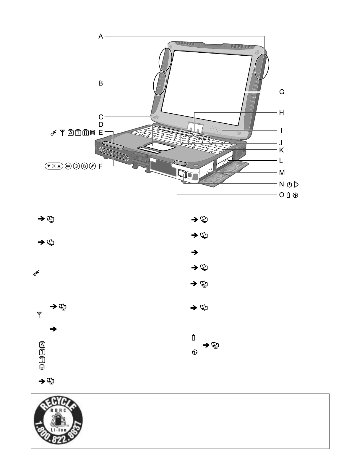
2-1
A: Wireless LAN Antenna
<Only for model with wireless LAN>
Reference Manual “Wireless LAN”
B: Bluetooth Antenna
<Only for model with Bluetooth>
Reference Manual “Bluetooth”
C: Stylus/Pen Holder
D: Touch Pad
E: LED Indicator
: Wireless ready
This indicator lights when Wireless LAN, Bluetooth, and/or Wireless WAN are connected and
ready. It does not necessarily indicate the On/Off
condition of the wireless connection.
Reference Manual “Wireless Switch Utility”
: Wireless WAN status
<Only for model with wireless WAN>
Refer to the instruction manual of the wireless
device.
: Caps lock
: Numeric key (NumLk)
: Scroll lock (ScrLk)
: Hard disk drive status
F: Tablet Buttons
Reference Manual “Tablet Buttons”
G: LCD
<Only for model with touchscreen>
Reference Manual “Touchscreen”
<Only for model with digitizer>
Reference Manual “Digitizer”
H: Display Release Latch
page 12 “Switching to the Tablet mode”
I: Speaker
Reference Manual “Key Combinations”
J: Function Key
Reference Manual “Key Combinations”
K: Keyboard
L: Hard Disk Drive
Reference Manual “Hard Disk Drive”
M: Battery Pack
N: Power Switch
O: LED Indicator
: Battery status
Reference Manual “Battery Power”
: Power status
(Off: Power off/Hibernation, Green: Power on,
Blinking green: Standby)
A lithium ion battery that is recyclable powers the product you have purchased.
Please call 1-800-8-BATTERY for information on how to recycle this battery.
L’appareil que vous vous êtes procuré est alimenté par une batterie au lithium-ion.
Pour des renseignements sur le recyclage de la batterie, veuillez composer le
1-800-8-BATTERY.
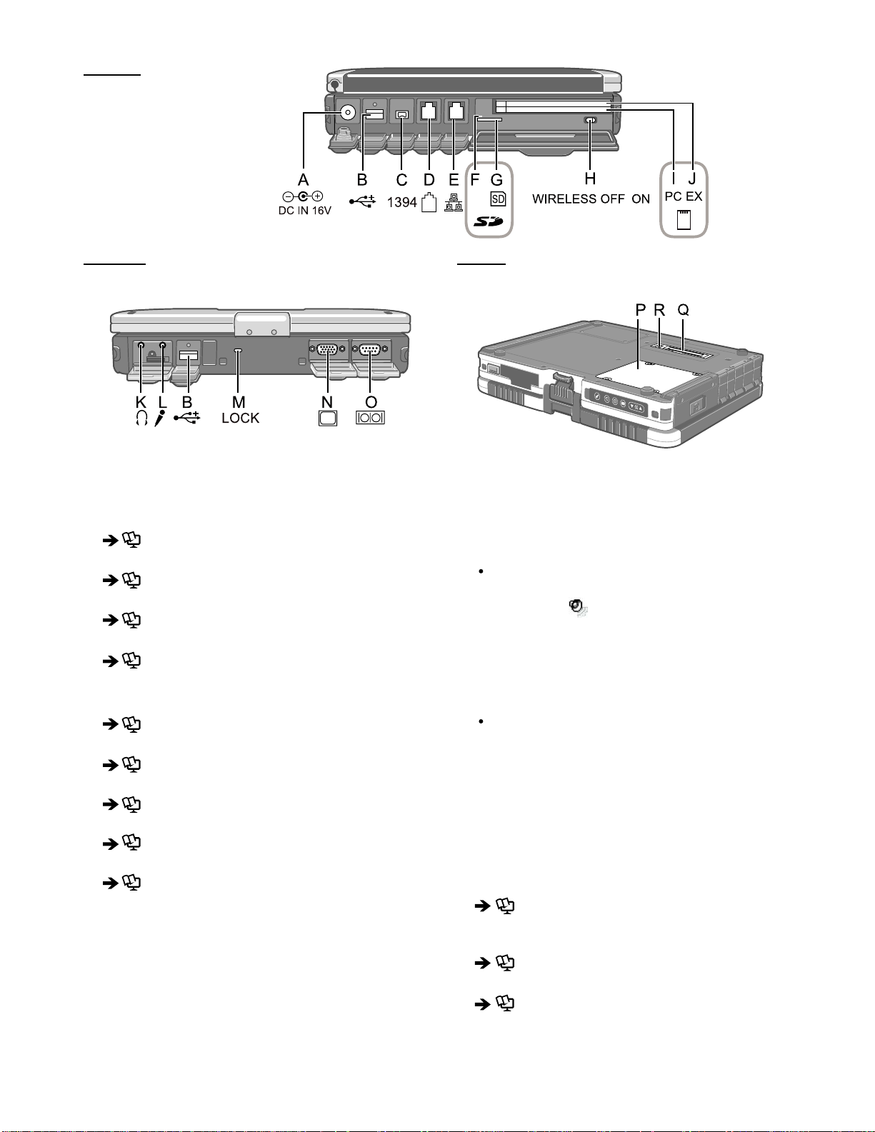
Left side
2-2
Rear side Bottom
A: DC-IN Jack
B: USB Port
Reference Manual “USB Devices”
C: IEEE 1394 Interface Connector
Reference Manual “IEEE 1394 Devices”
D: Modem Port
Reference Manual “Modem”
E: LAN Port
Reference Manual “LAN”
F: SD Memory Card Indicator
(Blinking: During access)
Reference Manual “SD Memory Card”
G: SD Memory Card Slot
Reference Manual “SD Memory Card”
H: Wireless Switch
Reference Manual “Wireless Switch Utility”
I: PC Card Slot
Reference Manual “PC Card / ExpressCard”
J: ExpressCard Slot
Reference Manual “PC Card / ExpressCard”
K: Headphone Jack
You can connect headphones or ampliÞ ed speakers.
When they are connected, audio from the internal
speakers is not heard.
L: Microphone Jack
A condenser microphone can be used. If other types
of microphones are used, audio input may not be possible, or malfunctions may occur as a result.
When recording in stereo using a stereo micro-
phone:
Double-click
in the notiÞ cation area, click [Options] - [Properties], and add a check mark for [Recording], click [OK] - [Options] - [Advanced Controls]
- [Advanced], remove a check mark for [Mono Microphone], and then click [Close].
When using a monaural microphone with a 2-termi-
nal plug:
With the settings outlined above, only audio on the
left track will be recorded.
When monitoring the microphone audio using headphones, sounds on the left track cannot be heard,
regardless of the above settings. This is a result of the
computer’s speciÞ cations, and is not a malfunction.
M: Security Lock
A Kensington cable can be connected.
For further information, read the manual that comes
with the cable.
N: External Display Port
Reference Manual “External Display”
O: Serial Port
P: RAM Module Slot
Reference Manual “RAM Module”
Q: Expansion Bus Connector
Reference Manual “Port Replicator / Car Mounter”
R: External Antenna Connector

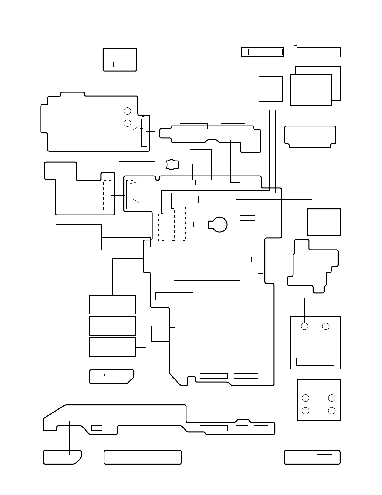
3 Block Diagram
(
)
p
r
B
p
ge
e
e
A
r
ge
t
5V
1.0
eake
S
P
AM
1
1
RJ
2 400
DDR
y
Main Memor
Hz
00M
hone
Ext. MIC
Head
0
l
920
C
gmate
A
Sound
Si
ST
5
.
Data Modem
MDC 1
y
r
2MB
51
B
2-3200
C
2G
P
SO-DIMM Extension Memo
Hz
00M
LAN
s
reles
i
W
)
1
5
8
C
5
d(R
Car
t
ar
m
S
A
I
C
PCM
ntenna
a
G
B
A
5
94
34
01L
1
8
RTL
lot
s
SD
1
43 / 85
C8
5
R
A/B/G
1
02.1
8
k
ealte
R
RICOH
45
RJ
TYPE II
D
R
sCA
Expres
.2
1
T
.2
35T
TPM 1
B96
L
S
uch
o
T
)
A
EC/KBC
(M306K
d
Pa
on
Infine
S/2
PR-P
e
KB& Mous
ger
har
C
y
tter
a
B
HDD
Li-Ion
Int. K
e
KBD Mous
Heater
ery
ck
tt
Pa
Ba
LED
p
PortRe
T
BKL
sor U2400
s
ch core
ea
s
e
t
tes
y
by
K b
4
2M
6
l
al
na
ltage 1.06GHz)
r
o
e
tern
: Int
e: In
h
c
che
a
c
ca
2
Intel® Core™ Duo mobile proce
(Ultra Low V
L1
L
V
l
e
onah UL
Dual core
int
AM
DR
Internal
LCD
S 1.8V 4
it BU
b
4
6
Interface
phics
Gra
XGA
10.4”
W
S
T
CR
S 1.8V 4
it BU
b
4
6
)
5
0
INTEL
(1.
Bridge
Host PCI
T
CR
C Link
T
CR
BIOS
p
PortRe
SPI
8
26
r I/O
0N
SMSC
Supe
SIO1
PCI
Brid
PCI-E
Brid
LPC
Interface
Interfac
)
Gb/s
5
(1.
5”
2.
1.5V
IDE
DMI
link
AC-
A
T
8M
SA
HDD
A
T
/ 120GB
0
8
SA
INTEL
Interfac
Bridge
USB 2.0
Interface
Prin
Finger
uch
o
T
Screen
Digitizer
F
ion I/
t
Configura
e
f
f
Bu
GPS
m
Mode
reless
i
W
Bluetooth
1
l
a
Seri
p
2
l
a
Seri
PortRe
ntenna
a
ntenna
a
0
2.
ntenna
a
3-1

4 Diagnosis Procedure
4-1
4.1. Basic Procedures

4.2. Troubleshooting
f
k
4-2
Please take note of the following two points with regard to troubleshooting:
1. Know-how of diagnosis upon occurrence of heavy troubles, e.g. Set cannot be turned ON , Set fails to start , No display on
screen , etc.
2. Explanation of each trouble, mainly symptom of trouble in operation.
Flow Chart
START
START
Pay attention to the following points when in pursuit of the cause of a troubleshooting.
1. Peripheral apparatus connected with the set should all be removed before operation check.
2. Make sure that cables, boards, etc. are not coming off, and recheck the contact condition.
Set cannot be supplied with current.
Power lamp fails to light up.
Dark display on screen.
Screen fails to display.
Failure in starting
Return set-up utility setpoint to the state of delivery from factory .
Not displayed properly on screen.
Some or all keys cannot be input.
Make sure of contact of K/B connector in use.
Replace keyboard or main board.
CD CALL not practicable.
Starts but operates unstably.
Reinstall HDD.
Replace main board.
AC
Adaptor/Battery
Output voltage
Power lamp
check
Inverter board
LCD back
light lighting
YES
LCD unit
check
OK
BIOS operation
chec
Result of
POST
Set-up utility
starting
OK
HDD access
YES
Main board
check
OK
Trouble
symptoms on some
of CD
YES
Replace main board.
OK
YES
OK
YES
OK
NO
NG
NO
NG
NO
NG
NG
NO
NG
NG
Replace AC Adaptor/Battery
Check contact condition of power input terminal. Replace i
defective.
Check Power SW. Replace if defective.
Replace inverter board.
Check inverter cable continuity. Replace if defective
Replace LCD back light.
Replace LCD unit.
Replace main board (Check fuse at power source).
Refer to POST
error code table.
Replace main board.
Check HDD cable connection and continuity.
Replace if defective.
Replace HDD & Reinstall.
Replace main board.
Replace main board
Check if there are any flaws on CD media. Since
NO
flaws may appear on specific media, CD media
can be defective.
Replace main board.
Heavy trouble e.g.,
Set cannot be turned
ON , Set fails to start ,
No display on
screen , etc.
Each kind of
trouble in
operation.
START
END

5 Power-On Self Test (Boot Check)
5-1
Outline of POST
The set has a boot check function called POST (Power-On Self Test) in it.
The condition of the main body is diagnosed by checking
Start .............Test begins automatically when power switch is set to ON.
Normal finish .....After memory checking, a beep sound is issued once and the set is placed into automatic stop.
Note: If no error occurs, nothing is displayed. (No display of OK, etc.)
Error Diagnosis by Checking Beep Signal Sound
The beep sound is as follows:
(Length of bar shows length of sound.)
beep sound or error code.
(1 (long sound) -2-3-4)
= long sound (about 0.4 sec.),
Table of errors classified by beep sounds
Diagnosis Beep signal sound Error message
Main board
(Note) A beep sound is also issued in case of other I/O trouble.
1(long sound)-2 BIOS ROM error
1-2-2-3
1-3-1-1
1-3-1-3
1-3-4-1
1-3-4-3
1-4-1-1
= short sound (about 0.2 sec.), Length between sounds is about 0.1 sec.
BIOS ROM error
RAM error
Keyboard controller error
RAM error
RAM error
RAM error
BIOS ROM error2-1-2-3
Occurrence of unexpected offering2-2-3-1

6 List of Error Codes <Only when the port replicator is connected>
6-1
The following is a list of the messages that BIOS can display. Most of them occur during
POST. Some of them display information about a hardware device, e.g., the amount of memory
installed. Others may indicate a problem with a device, such as the way it has been configured.
Following the list are explanations of the messages and remedies for reported problems.
If your system displays one of except the messages marked below with an asterisk (*), write
down the message and contact Panasonic Technical Support. If your system fails after you
make changes in the Setup menus, reset the computer, enter Setup and install Setup defaults
or correct the error.
0200 Failure Fixed Disk
Fixed disk in not working or not configured properly. Check to see if fixed disk is attached
properly. Run Setup. Find out if the fixed-disk type is correctly identified.
0210 Stuck key
Stuck key on keyboard.
0211 Keyboard error
Keyboard not working.
0212 Keyboard Controller Failed
Keyboard controller failed test. May require replacing keyboard controller.
0213 Keyboard locked - Unlock key switch
Unlock the system to proceed.
0230 System RAM Failed at offset : nnnn
System RAM failed at offset nnnn of in the 64k block at which the error was detected.
0231 Shadow RAM Failed at offset : nnnn
Shadow RAM failed at offset nnnn of the 64k block at which the error was detected.
0232 Extended RAM Failed at offset : nnnn
Extended memory not working or not configured properly at offset nnnn.
0250 System battery is dead - Replace and run SETUP
The CMOS clock battery indicator shows the battery is dead. Replace the battery and run Setup
to reconfigure the system.
*0251 System CMOS checksum bad - Default configuration used
System CMOS has been corrupted or modified incorrectly, perhaps by an application program
that changes data stored in CMOS. The BIOS installed Default SETUP Values. If you do not
want these values, enter Setup and enter your own values. If the error persists, check the system
battery or contact Panasonic Technical Support.
0260 System timer error
The timer test failed. Requires repair of system board.
0270 Real time clock error
Real-time clock fails BIOS test. May require board repair.
*0280 Previous boot incomplete - Default configuration used
Previous POST did not complete successfully. POST loads default values and offers to run
Setup. If the failure was caused by incorrect values and they are not corrected, the next boot
will likely fail. On systems with control of wait states, improper Setup settings can also termi-
nate POST and cause this error on the next boot. Run Setup and verify that the wait-state
configuration is correct. This error is cleared the next time the system is booted.
0281 Memory Size found by POST differed from EISA CMOS
Memory size found by POST differed from EISA CMOS.

02D0 System cache error - Cache disabled
6-2
Contact Panasonic Technical Support.
02F0: CPU ID:
CPU socket number for Multi-Processor error.
02F4: EISA CMOS not writable
ServerBIOS2 test error: Cannot write to EISA CMOS.
02F5: DMA Test Failed
ServerBIOS2 test error: Cannot write to extended DMA (Direct Memory Access) registers.
02F6: Software NMI Failed
ServerBIOS2 test error: Cannot generate software NMI (Non-Maskable Interrupt).
02F7: Fail - Safe Timer NMI Failed
ServerBIOS2 test error: Fail-Safe Timer takes too long.
device address Conflict
Address conflict for specified device.
Allocation Error for: device
Run ISA or EISA Configuration Utility to resolve resource conflict for the specified device.
Failing Bits : nnnn
The hex number nnnn is a map of the bits at the RAM address which failed the memory test.
Each 1 (one) in the map indicates a failed bit. See error 230,231 or 232 for offset address of the
failure in System, Extended or Shadow memory.
Invalid System Configuration Data
Problem with NVRAM (CMOS) data.
I/O device IRQ conflict
I/O device IRQ conflict error.
Operating System not found
Operating system cannot be located on either drive A: or drive C:. Enter Setup and see if fixed
disk and drive A: are properly identified.
Parity Check 1 nnnn
Parity error found in the system bus. BIOS attempts to locate the address and display it on the
screen. If it cannot locate the address, it displays ????. Parity is a method for checking errors
in binary data. A parity error indicates that some data has been corrupted.
Parity Check 2 nnnn
Parity error found in the I/O bus. BIOS attempts to locate the address and display it on the
screen. If it cannot locate the address, it displays ????.
Press <F1> to resume, <F2> to Setup
Displayed after any recoverable error message. Press <F1> to start the boot process or <F2> to
enter a Setup and change the settings. Write down and follow the information shown on the
screen.
Troubleshooting

7 Self Diagnosis Test
7-1
As for the self-diagnosis test(PC-Diagnostic utility) to use this model, a standard test and the
enhancing test by the module of the main body building in are possible.
Notes
1. Beginning of self-diagnosis test
1-1. Setting of content of setup
The power supply of the computer is turned on.
1.
" F2 " is pushed on the screen of "Panasonic" while " press <F2 to enter Setup> " is displayed.
2.
The setup utility starts and then takes notes of the content of the BIOS setup of present set.
3.
" F9 " is pushed, " Yes" is selected on the screen of " Is the default value loaded? ", and " Enter"
4.
is pushed.
" F10 " is pushed.
5.
" Yes" is selected on the screen of the setup confirmation, and " Enter" is pushed.
6.
The computer starts automatically.
7.
Attention
If the device which can be set is set to "Invalidity" by "Advanced" or "Security" menu, becomes an
error by "PC-Diagnostic utility".
(It is judged that the device which can be set to "Invalidity" by "Main" menu such as "Flat pad" is
normal if the controller operates normally though sets to "Invalidity" by the setup. )
In the model with built-in DVD of the USB connection, even if DVD is normal, becomes an error if
legacy USB is set to "Invalidity"
To skip BIOS password
Use <Ctrl>+<F10> key to skip BIOS password or authentication of fingerprint.
This key is only for entering DIAG mode. Not available to boot the computer.
If customer set "HDD Lock", the DIAG program cannot perform HDD test.
*This key is for service purpose only. Do not disclose this information to unrelated others.
1-2. When you execute an automatic test
1.
"Ctrl" + "F7" is pushed while the "Panasonic" start screen is displayed after the computer is started.
2.
The test of all devices begins automatically by "PC-Diagnostic utility"’s starting.
Attention
It is a test which the customer who bought PC can execute. (As for HDD, the enhancing test is also
possible.)
A flat pad does not work for a while after starting "PC-Diagnostic utility".
The movement of a flat pad might become abnormal If after RAM begins from the CPU/System
test, a flat pad will be operated in about 30 seconds. In that case,restarts pushing"Alt" + "Ctrl" +
"Del" key. Or, please start "PC-Diagnostic utility" again after doing the power supply switch in the
slide, and turning off the power supply.
1-3. When you execute the enhancing test
Please let me discontinue diagnosing clicking to end an automatic test.
1.
Please click on the character of "D" "PC-Diagnostic utility" on the screen while pushing both of right
2.
"Shift" and left "Shift" keys.
D
All devices which can select the enhancing test make the setting of the enhancing test possible.
3.
The district device is made"FULL" display (enhancing test).
4.
The test begins clicking .
5.
*Please refer to item 4 for the error result of each test and the division of the breakdown part.
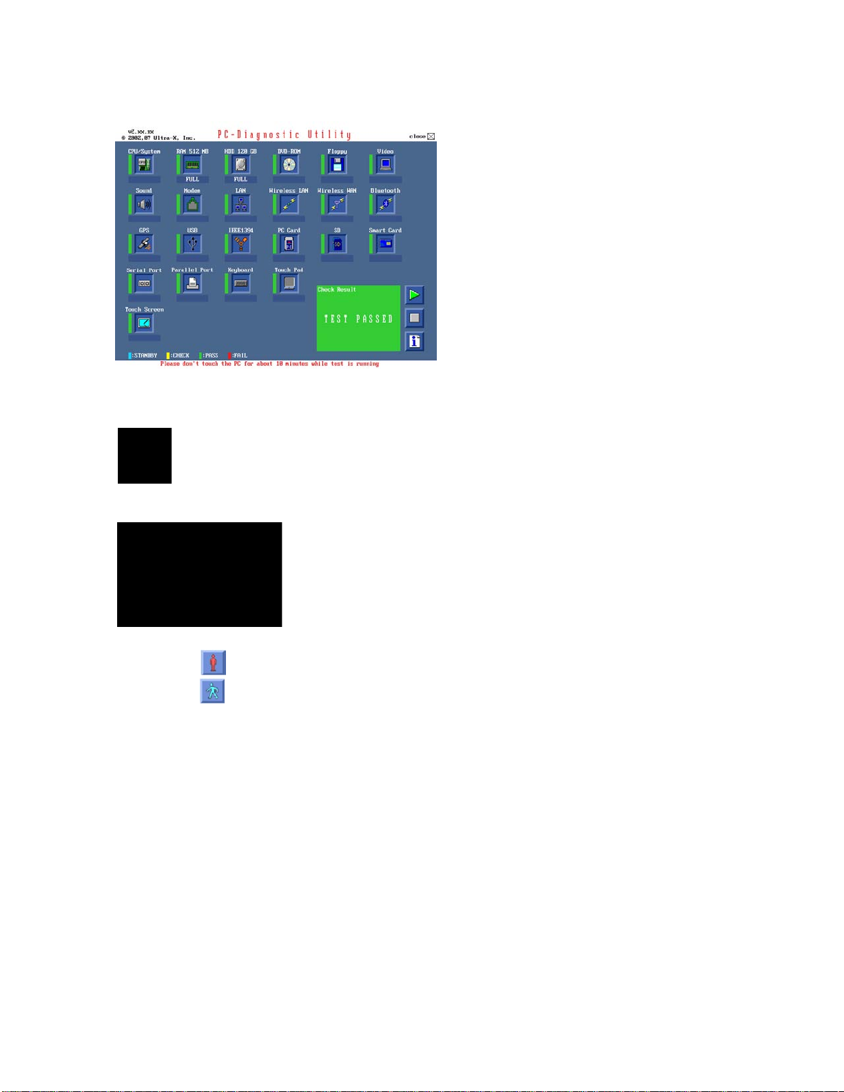
2. Operation of PC-Diagnostic Utility
7-2
-Only the device which can be inspected on the entire screen is displayed.
-The item does not appear when the device of wireless LAN etc. is not physically connected.
-The movement of the item must use an arrow key or a flat pad.
-As for the device under the diagnosis, blue and yellow are alternately displayed at the left of the icon.
- The diagnosis result of the device greens at the left of the icon when it is normal, and becomes red when
abnormal.
-When the test of all devices ends, the test result is displayed under the right of the screen.
-Please click while diagnosing when being stop on the way by the time the test of all devices ends.
-Please click when you restart "PC-Diagnostic utility".
*Each device is tested from the beginning, and it is not possible to restart on the way.

2-1. Selection of tested device
7-3
-To test only a specific device, "Test" and "Do not test" of each device can be selected.
-The device which can select the enhancing test changes in order of "The standard is tested" and "Do not
test" whenever the device icon is clicked.
Start the standard test
Please begin testing clicking if the selection of the tested device ends.
Do not test
2-2. "PC-Diagnostic utility" End method
When of "Close" on the right of the screen is clicked, the computer reactivates automatically. Or, the
power supply switch is done in the slide and the power supply is turned off.
2-3. The content of the setup is returned to the setting of the user
Turned on the computer.
1.
"F2" is pushed on the screen while "Press<F2>to enter Setup" is displayed of "Panasonic".
2.
Push "F10", and on the screen of "Is the change in the setting preserved and do end?"and then "Yes"
3.
is selected, and "Enter" is pushed.
The computer reactivates automatically.
4.
The end option is chosen by the start menu, and the power supply of the computer is turned off.
5.
Standard at test time
All devices other than RAM and HDD
RAM standard test
HDD standard test
HDD enhancing test (60GB)
about 1 minute
1 - 2 minutes
2 - 3 minutes
about 40 minutes
Ex.The standard when the standard <all device> is tested becomes 1+2+3=6 minutes.
There is greatly a difference from RAM test when the memory is increased according to the performance of the memory occasionally.
Moreover, when the main body of PC under the test is a high temperature, it occasionally takes time.
There is greatly a difference from HDD according to the performance of the drive occasionally.

7.1. Test Item and Division of trouble
7-4
Test item Stanard
CPU /
SYSTEM
RAM All memory space is tested in a spe-
HDD The record area frequently accessed
MODEM It is confirmed not to find abnormality
Wireless
LAN
Enhancing
Content of standard test Content of enhancing test
CPU is shifted to protected mode, and
"Violation of the paging", "Operation of
the violation of a privileged instruction", and DMA, INT, TIMER, and the
RTC operation are confirmed.
cial memory access pattern based on
"R.S.T . technology".
with Microsoft Windows XP to test in
about two minutes regardless of
points of HDD is emphatically tested.
in the AC97 modem controller.
It is confirmed not to find abnormality
in the Wireless LAN modem controller.
Place with possibili-
ty of breakdown
CPU /
Main board
Memory / Mainboard
All record area is tested. HDD /
Mainboard /
Cable /
Connector
MODEM/ Mainboard
Wireless LAN
board /
Connector /
Mainboard
Sound
*5
USB It is confirmed not to find abnormality
in the USB controller.
*1
LAN It is confirmed not to find abnormality
in the LAN controller.
*2
PC Card It is confirmed not to find abnormality
in the CardBus controller.
SD It is confirmed not to find abnormality
in the SD controller.
Keyboard It is confirmed not to find abnormality
*3
in keyboard controller’s keyboard interface.
It is confirmed not to find abnormality in the wiring between the USB controller and
the connector by confirming
the connection of the USB
equipment connected with the
USB connector.
It is confirmed not to find abnormality in the wiring between the controller and the
connector by connecting to
HUB with LAN cable.
The key is actually input, and
the operation is displayed on
the screen.
Mainboard /
Connector
Mainboard /
Connector
Mainboard
Mainboard
Mainboard /
Keyboard
Touch Pad
DVD-ROM
Whether keyboard controller’s mouse
*4
interface operates normally is confirmed.
*6
The drive is normally reset, and it is
accessible is confirmed.
The operation is actually displayed on the screen by operating the touch pad.
It is confirmed to be able to
read media normally.
Mainboard /
Touch Pad
Mainboard /
Touch Pad

Test Item
7-5
Touch Screen
Standard Enhanced
Content of Standard Test Content of Extend Test
It is confirmed not to find
abnormality in the USB
connection of Touch Screen.
This test cannot find
abnormality of Touch Screen.
Perform Touch Screen
functionality practically.
Operator has to judge
PASS/FAIL with test result.
It is confirmed not to find
Bluetooth
abnormality in the connection
of Main board and Bluetooth
module.
It is confirmed not to find
Wireless WAN
abnormality in the connection
of Main board and Wireless
WAN module.
It is confirmed not to find
abnormality in the legacy FD
Floppy
drive.
This test cannot find
abnormality of mechanical
breakdown. (e.g.. Head, Motor)
It is confirmed not to find
abnormality in access to
Video
VRAM with VESA.
The PC which uses main
memory as VRAM may fail with
main memory failure.
It is confirmed not to find
GPS
abnormality in the connection
of Main board and GPS
It is confirmed not to find
IEEE1394
abnormality in the IEEE1394
controller.
It is confirmed not to find
Express Card
abnormality in the wiring
between Chipset and Express
Card.
It is confirmed not to find
Smart Card
abnormality in the Smart Card
controller.
It is confirmed not to find
abnormality of Super I/O
Serial Port *7
UART function.
This test cannot find lack of
wiring between Super I/O and
Serial Connector.
It is confirmed not to find
abnormality of Super I/O
Parallel Port *8
parallel function.
This test cannot find lack of
wiring between Super I/O and
Parallel Connector.
*1
Please connect the USB device with the port (USB connector) which wants to test before the tests.
*2
Please connect LAN port with LAN HUB with LAN cable before the tests.
The operator actually inputs the key, and the operator judges PASS/FAIL of the test.
*3
The operator actually operates the mouse, and the operator judges PASS/FAIL of the test.
*4
It is not abnormal though the sound is emitted from the speaker while testing.
*5
It is confirmed not to find
abnormality in the wiring
between Super I/O and Serial
Connector.
This test cannot find failure of
cable characteristic and device
problems.
It is confirmed not to find
abnormality in the wiring
between Super I/O and
Parallel Connector.
This test cannot find failure of
cable characteristic and device
problems.
When the test result is PASS, trouble is thought by not hearing of the sound under the test from
the speaker and the headphone by the wiring of the audio output system.
*6
Please set DVD/CD media in the drive before the tests.
*7 Please set a Special Loop Back Connector Tool at serial connector for Enhanced Test.
(This Connector Tool is same as the one used before.)
*8 Please set a Special Loop Back Connector Tool at parallel connector for Enhanced Test.
(This Connector Tools is same as the one used before.)
The place with possibility of
breakdown
Main board/
Touch Screen
Bluetooth cable
WWAN cable
FD Drive/
Main board (Super I/O)/
FDD cable
FDD connector
Main board
(Chipset, Graphic
Controller)/
Memory
GPS cable
Main board
(IEEE#394 Controller)
Main board (Chipset)/
Express Card Connector
Main board
(Smart Card Controller)
Main board (Super I/O)/
Serial Connector
Main board (Super I/O)/
Parallel Connector
8 Wiring Connection Diagram
8-1
HSDPA PCB
H/P MIC
AUDIO PCB
KEYBOARD
CN901
BT PCB
CN1
JK601
JK600
CN604
CN600
CN16
CN27
RTC
BATTERY
CN17
CN5
EXTERNAL
DISPLAY
PORT
CN882 CN881
CN9 CN14
CN18
CN8
CN23
CN3
MAIN PCB
SERIAL PORT
CN883CN880
COIN
BATTERY
INVERTER PCB
CN1 CN2
TS PS2 PCB
CN901
CN900
JK880
DC-IN
I/O PCB
CN24
CN21
CN12
LAN
PORT
BACK LIGHT
LCD
Touch
Screen
Panel
I/F PCB
CN850
MODEM
PCB
SD PCB
CN891
CN806
RIGHT
LED PCB
CN841
PAD PCB
HDD
MAIN
BATTERY
PCMCIA UNIT
POWER SW PCB
CN980
CN804
SW PCB
CN11
TOUCH PAD
CN800
CN950
CN4
CN15
CN23
CN802
CN15
HDD
FPC BAT
CN805
LANAUX
WIRELESS
MODULE
J1
ANT PCB
GPRS
LANMAIN
CN801
LEFT LED PCB
CN780

9 Disassembly/Reassembly
Note:
Power off the computer. Do not shut down to the Suspend or hibernation mode.
Do not add peripherals while the computer is in the Suspend or hibernation mode; abnormal operation may result.
9.1. Disassembly Instructions
9.1.1. Preparation
Before disassembling, be sure to make the following preparations.
• Shut down Windows and turn off the power.
• Disconnect the AC adaptor.
• Remove the optional DIM M mem ory car d and PCMC IA card
if they are connected.
• Remove other devices if they are connected.
Attention:
• Please execute writing BIOS ID when you exchange the
Main Board.
• Parts (Sheet and rubber) etc. rel ated various the Conducti ve
Cloth and Heat Spreader cannot be recycled. Use new p art s.
9.1.2. Removing the Battery Pack and
HDD Pack
1
2
3
HDD Case B
Hooks
HDD FPC
HDD
Heater
<N13>
<N13>
HDD Case A
5. Remove the two Screws <N13>.
6. Remove the HDD Case A and the HDD Case B.
7. Remove the HDD
Screws <N13> : DXQT2+D4FNL
Hooks
Battery Pack
1. Open the Battery Cover.
2. Remove the Battery Pack.
3. Open the HDD Cover.
4. Remove the HDD Pack.
HDD Pack
9.1.3. Removing the Touch Pad and Keyboard
KBD Plate
<N9>
<N9>
Palm Rest Ass’y
1. Remove the Palm Rest Ass'y.
Note:
The Palm Rest Ass'y is firmly fixed with two-sided
tape.
Carefully remove the Palm Top Cover Sheet not to
damage it.
2. Remove the 4 Screws <N9>.
3. Remove the KBD Plate.
KBD Plate
<N9>
<N9>
9-1
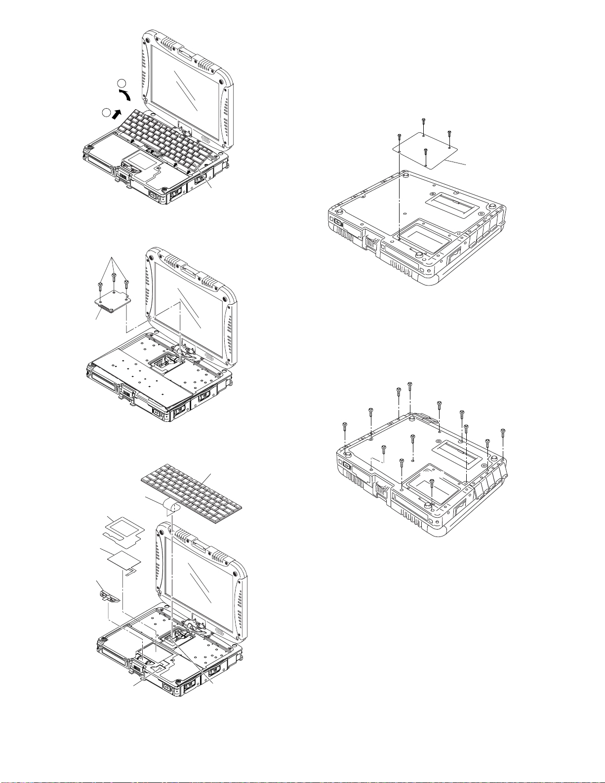
10. Disconnect the Cable from Connector (CN800).
y
11. Remove the Touch Pad and Click Button Plate.
Screws <N1> : DFHE5025XA
Screws <N9> : DRSB2+5FKL
1
9.1.4. Removing the DIMM Lid Ass’y
2
Keyboard
4. Lift the far side of the Keyboard and slide it to backward,
and then turn the Keyboard over frontward.
<N1>
KBD
Connector
Cover
5. Remove the 3 Screws <N1>.
6. Remove the KBD Connector Cover.
Keyboard
<K14-8>
<K14-8>
<K14-8>
<K14-8>
DIMM Lid Ass’
1. Remove the 4 Screws <K14-8>.
2. Remove the DIMM Lid Ass'y.
Screws <K14-8> : DRHM5025YAT
9.1.5. Removing the Rear Cabinet
<N10>
<N10>
<N10>
<N10>
<N10>
<N10>
<N10>
<N10>
<N10>
<N10>
<N10>
<N10>
<N10>
Keyboard
FPC
TP Tape
Touch Pad
Click Button
Plate
Connector
(CN800)
Connector
(CN18)
7. Disconnect the Cable from Connector (CN18).
8. Remove the Keyboard.
9. Remove the TP Tape.
1. Remove the 13 Screws <N10>.
2. Open the LID Rubbers.
3. Remove the Rear Cabinet.
Screws <N10> : DRHM0061ZA
9-2
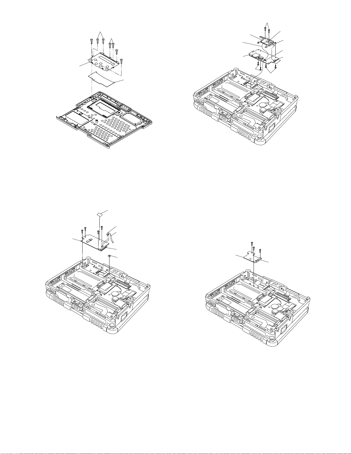
9.1.6. Removing the DU Lid Unit
<K14-9>
<K14-9>
DIMM Lid Angle
<K14-9>
<K14-9>
<K14-9>
DU Lid
Bluetooth PCB
Antenna Cable(blue)
HSDPA PCB
<N19>
Connector(CN1)
Plate
Clamper
Connector(CN604)
<N19>
<N19>
1. Remove the 7 Screws <K14-9>.
2. Remove the DU Lid Angle and DU Lid.
Screws <K14-9> : DXQT2+D25FNL
9.1.7. Removing the HSDPA PCB and
Bluetooth PCB
Tape
<N9>
<N9>
Antenna Cable(brown)
Antenna Cable(black)
Connector(CN600)
Cable Holder Cushion
HSDPA PCB
<N9>
<N9>
6. Disconnect the Antenna Cable from the Clamper.
7. Disconnect the Antenna Cable.
8. Remove the 4 Screws. <N19>
9. Disconnect the Cable from the Connector (CN604).
10. Remove the 2 Screws. <N19>
11. Disconnect the Cable from the Connector (CN1) and
remove the Bluetooth PCB and HSDPA PCB.
Screws <N9> : DRSB2+5FKL
Screws <N19> : XSB2+3FNL
9.1.8. Removing the Audio PCB
<N9>
<N9>
Audio PCB
<N9>
Connector(CN901)
1. Remove the Cable Holder Cushion.
2. Disconnect the 2 Antenna Cables (brown, black).
3. Remove the Tape.
4. Remove the 4 Screws. <N9>
5. Disconnect the Cable from the Connector (CN600).
1. Remove the 3 Screws <N9>.
2. Disconnect the Cable from a Connector (CN901).
3. Remove the Audio PCB.
Screws <N9>:DRSB2+5FKL
9-3

9.1.9. Removing the Main PCB, Wireless
Module, SD PCB, Antenna PCB and
Modem PCB
Connector(CN8)
Connector(CN17)
Note:
This procedure is not necessary if the computer is not
equipped with Wireless Module or Modem PCB.
1. Disconnect the 2 LCD Cables. (CN8,CN17)
<N8>
<N9>
Connector(CN15)
<N8>
<N9>
HDD
Connector Guide
<N19>
<N19>
Connector(CN21)
SD PCB Ass’y
BAT FPC Ass’y
DU PCB
<N3>
<N3>
<N9>
<N9>
Antenna PCB
<N3>
gray cable black cable white cable
<N9>
Plate
<N3>
2. Remove the gray, black and white Antenna Cables.
3. Remove the 2 Screws <N3> and the 3 Screws <N9>.
4. Remove the 2 screws <N3>, and remove the DU PCB,
Plate and Antenna PCB.
5. Remove the 2 Screws <N8>, and remove the HDD Connector Guide.
6. Remove the 2 Screws. <N9>
7. Disconnect the Cable from the Connector. (CN15)
8. Remove the BAT FPC Ass'y.
9. Remove the 3 Screws. <N19>
10. Disconnect the Cable from the Connector (CN21), and
remove the SD PCB Ass'y.
<N19>
<N19>
<N19>
Modem PCB
Coin Battery
DIMM Holder
<N19>
Wireless Module
<N19>
<N19>
Connector(CN3)
11. Disconnect the Cable from the Connector (CN3), and
remove the Coin Battery.
12. Remove the 2 Screws <N19>, and remove the Wireless
Module.
13. Remove the 2 Screws <N19>, and remove the Modem
PCB.
9-4

14. Remove the 2 Screws <N19>, and remove the DIMM
Holder.
Screws <N2> : DFHE5058ZB
Screws <N9> : DRSB2+5FKL
Connector(CN23)
Tape
<N19>
<N19>
<N19>
<N19>
Connector(CN9)
Connector(CN14)
Main PCB
Combo Socket
9.1.11. Removing the Power SW PCB
<N1>
Connector(CN9)
Power SW
PCB
<N19>
1. Remove the Screw <N1>.
2. Disconnect the Cable from the Connector (CN9).
3. Remove the Power SW PCB.
Screw <N1> : DFHE5025XA
9.1.12. Removing the left LED and right
LED PCB
15. Remove the Tape.
16. Disconnect the 3 Cables from the 3 Connectors.
(CN9,CN14,CN23)
17. Remove the 7 Screws <N19>, and remove the Main PCB
and Combo Socket.
Screws <N3> : DFHE5108ZA
Screws <N8> : DRSB2+10FKL
Screws <N9> : DRSB2+5FKL
Screws <N19> : XSB2+3FNL
9.1.10. Removing the I/O PCB Ass'y
<N9>
I/O PCB Ass’y
<N2>
<N9>
<N2>
<N2>
<N2>
Release Paper
Release Paper
left LED PCB
Connector(CN806)
right LED PCB
Connector(CN801)
1. Remove the two Release Papers.
2. Disconnect the Cable from the Connector (CN806).
3. Remove the left LED PCB.
4. Disconnect the Cable from the Connector (CN801).
5. Remove the right LED PCB.
1. Remove the 4 D-SUB Screws <N2>.
2. Remove the 2 Screws <N9>.
3. Remove the I/O PCB Ass'y.
9-5
 Loading...