

Page 1
ORDER NO. CPD0606050C1
Wireless Display
CF-08TX1A1M
This is the Service Manual for
the following areas.
M …for U.S.A.
© 2006 Matsushita Electric Industrial Co., Ltd. All rights
reserved. Unauthorized copying and distribution is a violation
Page 2
1
Page 3
2
Page 4
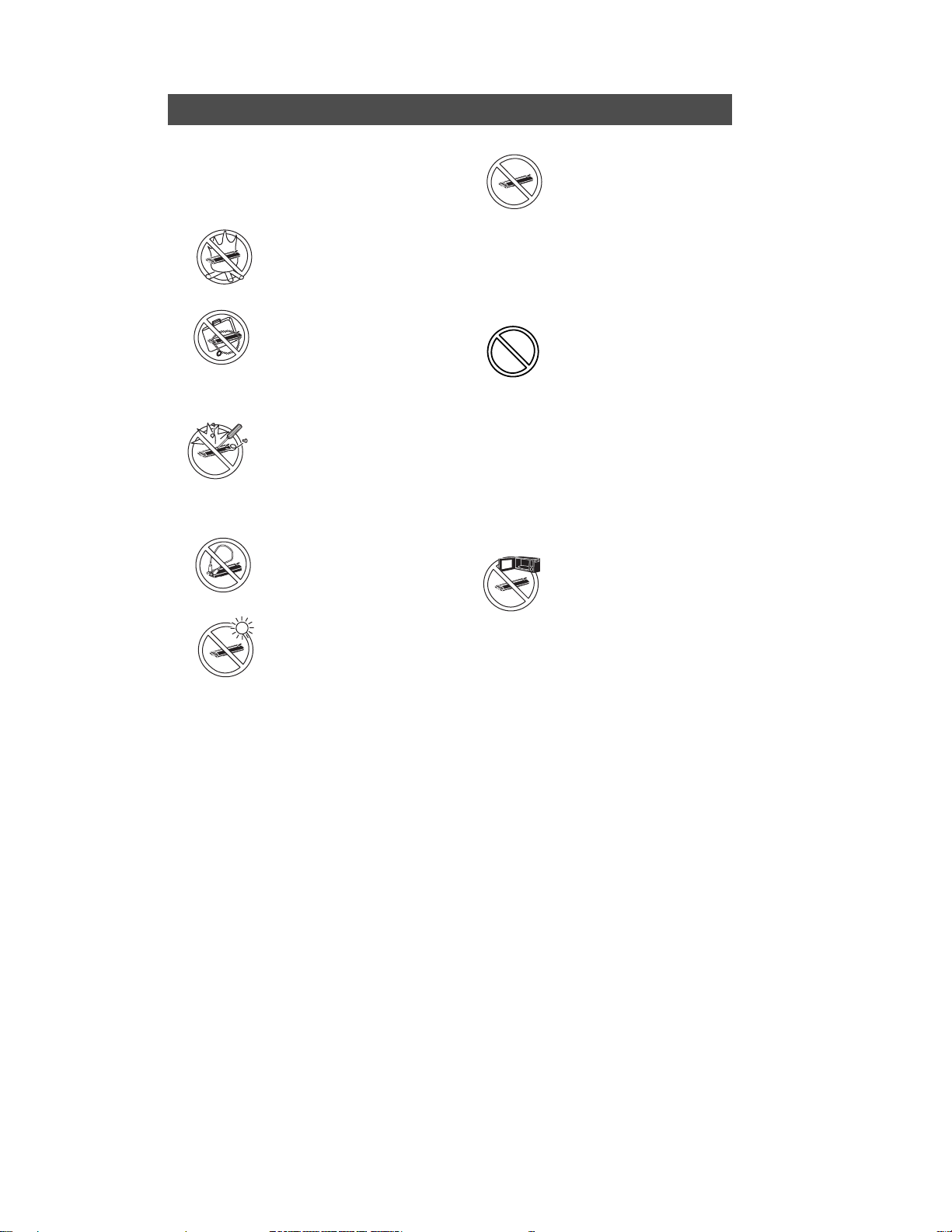
Precautions
Battery Pack
Care should be exercised with
regard to the following in order to
avoid the possibility of overheating,
fire or damage.
Avoid Heat
Do not throw the battery
pack into a fire or expose
it to excessive heat.
Keep Articles Away
Do not place the battery
pack together with articles such as necklaces
or hairpins when carrying or storing.
Do Not Disassemble
Do not insert sharp
objects into the battery
pack, expose it to bumps
or shocks, deform, disassemble, or modify it.
Do Not Short
Do not short the positive
(+) and negative (-) contacts.
Avoid Extreme Heat,
Cold and Direct Sunlight
Do not charge, use or
leave the battery pack for
extended periods where
it will be exposed to
direct sunlight, in a hot
place (in a car on a
sunny day, for example),
or in a cold place.
Do Not Use With Any
Other Equipment
The battery pack is
rechargeable and was
intended for the specified equipment. Do not
use it with any equipment
other than the one for
which it was designed.
Do Not Use This Wireless Display with a Battery Pack Other Than
the One Specified
Use only the specified
Panasonic battery pack
(CF-VZSU44U) with your
CF-08. Use of batteries
other than those manufactured and supplied by
Panasonic may represent a safety hazard.
Do Not Put into a Microwave
Do not put the battery
pack into a microwave
oven or a pressurized
chamber.
3
Page 5

Stop Using
Should the battery emit
an abnormal odor,
become hot to the touch,
become discolored,
change shape, or
become in any way different from normal,
remove it from the wireless display and stop
using it.
Do not touch the terminals on the
battery pack. The battery pack may
no longer function properly if the
contacts are dirty or damaged.
Do not expose the battery pack to
water, or allow it to become wet.
If the battery pack will not be used
for a long period of time (a month or
more), charge or discharge (use) the
battery pack until the remaining battery level becomes 30% to 40% and
store it in a cool, dry place.
This wireless display prevents overcharging of the battery by recharging
only when the remaining power is
less than approx. 95% of capacity.
The battery pack is not charged
when the wireless display is first purchased. Be sure to charge it before
using it for the first time. When the
AC adaptor is connected to the wireless display, charging begins automatically.
Should the battery leak and the fluid
get into your eyes, do not rub your
eyes. Immediately flush your eyes
with clear water and see a doctor for
medical treatment as soon as possible.
NOTENOTE
The battery pack may become warm
during recharging or normal use.
This is completely normal.
Recharging will not commence if
internal temperature of the battery
pack is outside of the allowable temperature range (0 °C to 45 °C {32°F
to 122°F}). Once the allowable range
requirement is satisfied, charging
begins automatically. Note that the
recharging time varies based on the
usage conditions. (Recharging takes
longer than usual when the temperature is 10 °C {50°F} or below.)
If the temperature is low, the operating time is shortened. Only use the
equipment within the allowable temperature range.
The battery pack is a consumable
item. If the amount of time the equipment can be run by using a particular
battery pack becomes dramatically
shorter and repeated recharging
does not restore its performance, the
battery pack should be replaced with
a new one.
When transporting a spare battery
inside a package, briefcase, etc., it is
recommended that it be placed in a
plastic bag so that its contacts are
protected.
Always power off the equipment
when it is not in use. Leaving the
equipment on when the AC adaptor
is not connected will exhaust the
remaining battery capacity.
4
Page 6

CONTENTS
1. Specifications ··················································································································1-1
2. Introduction······················································································································2-1
3. Description of parts ·········································································································3-1
4. Starting up/Shutting Down·······························································································4-1
5. Diagnosis & Repair··········································································································5-1
6. Troubleshooting···············································································································6-1
7. Block Diagram ·················································································································7-1
8. Wiring Connection Diagram ····························································································8-1
9. Disassembly/Reassembly ·····························································································9-1
10. Exploded View·············································································································10-1
11. Replacement Parts List ·······························································································11-1
Page 7
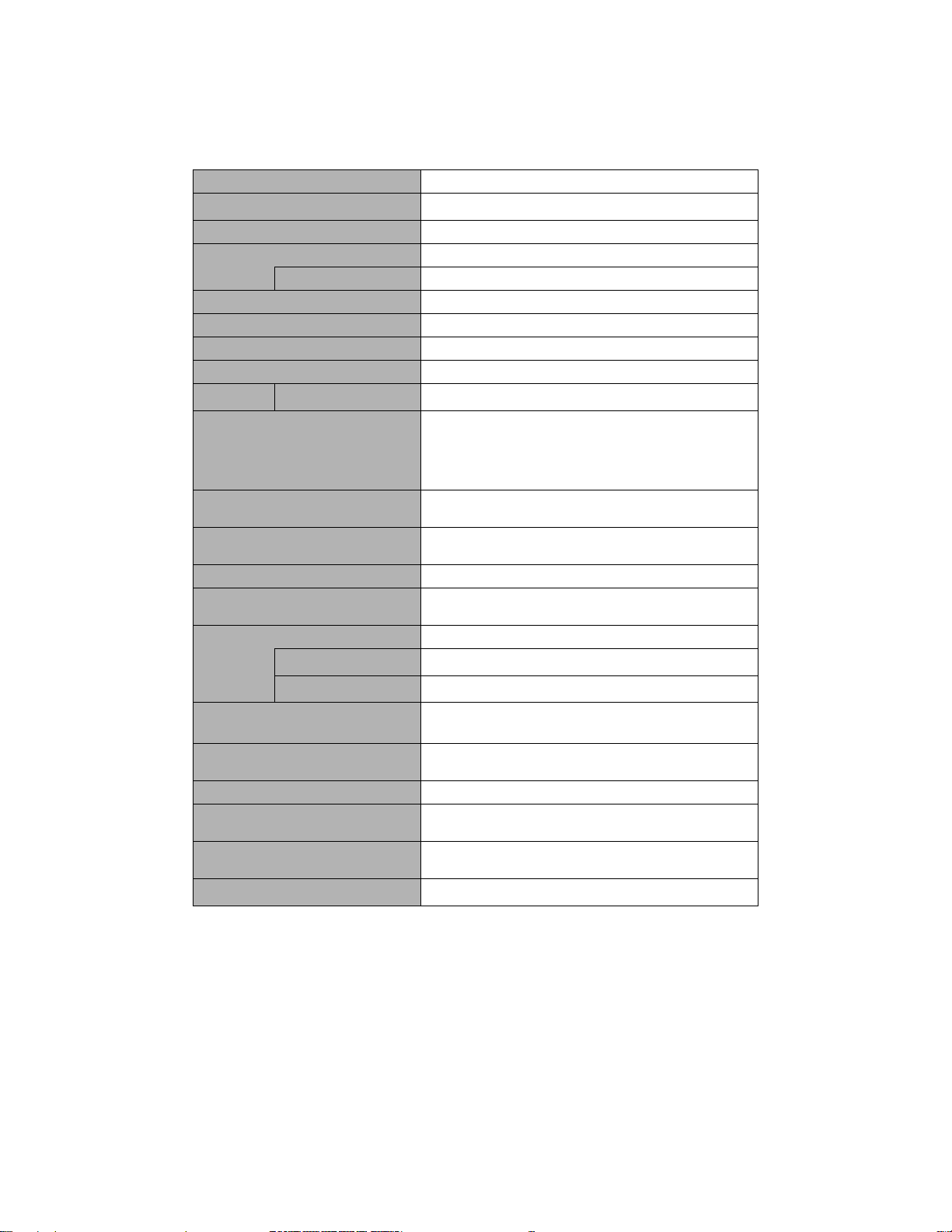
1 Specifications
Main Specifications
Model No. CF-08TX1A1M
CPU
Memory (ROM/RAM) 32 MB (Flash) /64 MB
Display Method 10.4 XGA type
Internal LCD Display 65,536 colors (1024 × 768 pixels)
Wireless LAN Built-in
Bluetooth Built-in
LAN IEEE 802.3 10Base-T, IEEE 802.3u 100Base-TX
Sound WAVE playback, Monaural speaker
Card Slot
Interface USB Port × 1 (USB1.1), LAN Port (RJ-45), Expan-
Button Power button, USER button, Keyboard button,
Pointing Device Touchscreen (Anti-Reflection, Stylus (included)
Power Supply AC adaptor or Battery pack
AC Adaptor
Battery Pack Li-ion 7.4 V, 5.2 Ah
Power Consumption
Physical Dimensions (W × H × D) 267 mm × 208 mm × 36 mm (excluding protrusion)
Weight Approx. 1.2 kg {Approx. 2.6 lb.}
Operation Environment Temperature: 5 °C to 35 °C {41 °F to 95 °F}
Storage Environment Temperature: -20 °C to 60 °C {-4 °F to 140 °F}
Operating System
SD Memory Card
*3
Operating Time
Charging Time
Intel® PXA270 Processor 312 MHz
*1
× 1, Data transfer rate=4.8 MB per second
sion Bus Connector (Dedicated 16-pin), Microphone
Jack (Miniature jack, 3.5 DIA, Monaural), Headphone Jack (Miniature jack, 3.5 DIA, Impedance
32 , Output Power 4 mW × 2)
Cursor control button (with Enter key)
touch capable)
Input: 100 V to 240 V AC, 50 Hz/60 Hz
Output: 16.0 V DC, 2.5 A
*4
*4
*7
Approx. 4.5 hours to 14 hours*5 (Approx. 7 hours)
Approx. 4 hours
Approx. 10 W *8/ Approx. 30 W (Maximum when
recharging in the ON state)
{10.5 ’’ × 8.2 ’’ × 1.4 ’’}
Humidity: 30% to 80% RH (No condensation)
Humidity: 30% to 90% RH (No condensation)
Microsoft® Windows® CE 5.0 Professional
*2
*6
1-1
Page 8
Software
Microsoft
®
Remote Desktop Connection, Citrix®
ICA® Client, Microsoft® Internet Explorer 6.0
*1
This slot does not support the MultiMedia card.
Operation has been confirmed for Panasonic SD Memory Cards with up to 2 GB capacity.
*2
Theoretical value and not the actual speed. The transfer rate does not become higher
even if you use a card that supports the higher transfer rate.
*3
<Only for North America>
The AC adaptor is compatible with power sources up to 240 V AC adaptor. The wireless
display is supplied with a 125 V AC compatible AC cord.
*4
Varies depending on the usage conditions.
*5
Measured using BatteryMark™ Version 4.0.1 (LCD brightness: Maximum - Minimum)
*6
Measured using MobileMark™ 2002 (LCD brightness: 150 cd/m2)
*7
Approx. 0.9 W when the battery pack is fully charged (or not being charged) and the
wireless display is OFF.
*8
Rated power consumption
Wireless LAN
Data transfer rates
*9
11/5.5/2/1 Mbps (automatically switched)
Standards supported IEEE802.11b
Transmission method OFDM system, DS-SS system
Wireless channels used Channels 1 to 11
RF frequency band 2412-2462 MHz
*9
These are speeds specified in IEEE802.11b standards. Actual speeds may differ.
Bluetooth™
Bluetooth Version 1.2
Transmission Method FHSS system
Wireless Channels Used Channels 1 to 79
RF Frequency Band 2.402-2.48 GHz
1-2
Page 9

2 Introduction
Copyright
This manual is copyrighted by Matsushita Electric Industrial Co., Ltd. with all rights
reserved. No part of this manual may be reproduced in any form without the prior
written permission of Matsushita Electric Industrial Co., Ltd.
No patent liability is assumed with respect to the use of the information contained
herein.
© 2006 Matsushita Electric Industrial Co., Ltd. All Rights Reserved.
Disclaimer
Wireless display specifications and manuals are subject to change without notice.
Matsushita Electric Industrial Co., Ltd. assumes no liability for damage incurred
directly or indirectly from errors, omissions or discrepancies between the wireless
display and the manuals.
Trademarks
Microsoft
Microsoft Corporation of the United States and/or other countries.
SD Logo is a trademark.
Citrix
Bluetooth™ is a trademark owned by Bluetooth SIG, Inc., U.S.A. and licensed to
Matsushita Electric Industrial Co., Ltd.
Panasonic® is a registered trademark of Matsushita Electric Industrial Co., Ltd.
Names of products, brands, etc., appearing in this manual are trademarks or registered trademarks of their respective own companies.
®
, Windows® and the Windows logo are registered trademarks of
®
and ICA® protocol are registered trademarks of Citrix Systems, Inc.
2-1
Page 10
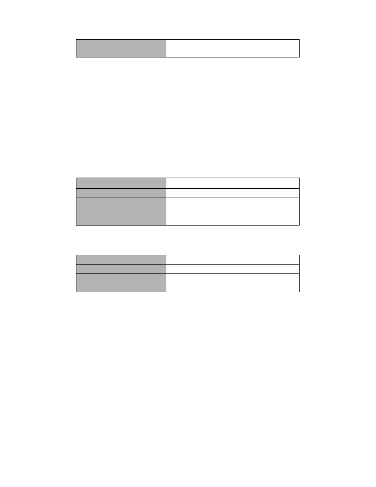
3 Description of parts
A. LCD (Touchscreen)
B. Wireless LAN antenna
C. Bluetooth antenna
D. Power status
E. Power button
F. Battery status
G. DC- IN j ac k
A. Battery cover latch
B. Hand strap
Adjust the length of the belt so that
the wireless display does not fall
by mistake, and firmly hold the
wireless display when using it.
C. Battery pack
D. Headphone jack
You can connect headphones or
amplified speakers. When they are
connected, audio from the internal
speakers is not heard.
E. Microphone jack
Use only monaural condenser
microphone (miniature jack). Connecting another type of microphone may interrupt audio input or
may cause a malfunction.
F. Stylus holder
G. Security lock
You can connect a Kensington
cable. Refer to the instruction
manual of the cable.
H. Speaker
I. Expansion bus connector
H. LAN port
I. Cursor control button
J. Keyboard button
K. USB port
L. USER button
M. SD Memory Card slot
N. SD Memory Card status
CAUTION
Do not put metallic objects or magnetic media close to the speaker.
Do not touch the expansion bus connector. The wireless display may no longer
function properly if the connector is dirty or damaged.
3-1
Page 11
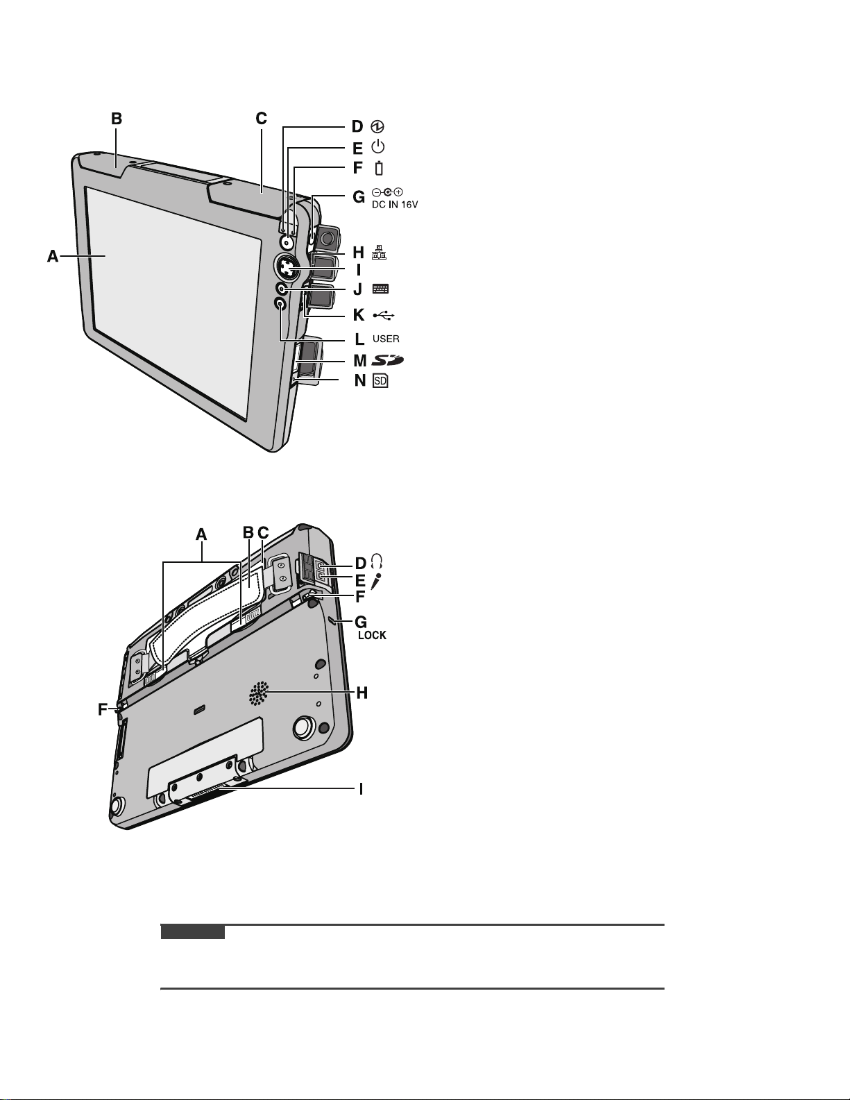
Using the Tether
Attaching the Tether
The tether can be attached to the upper right
or upper left corner of the display. It prevents
the pen (included) from falling accidentally.
1
2
3
4
3-2
Page 12
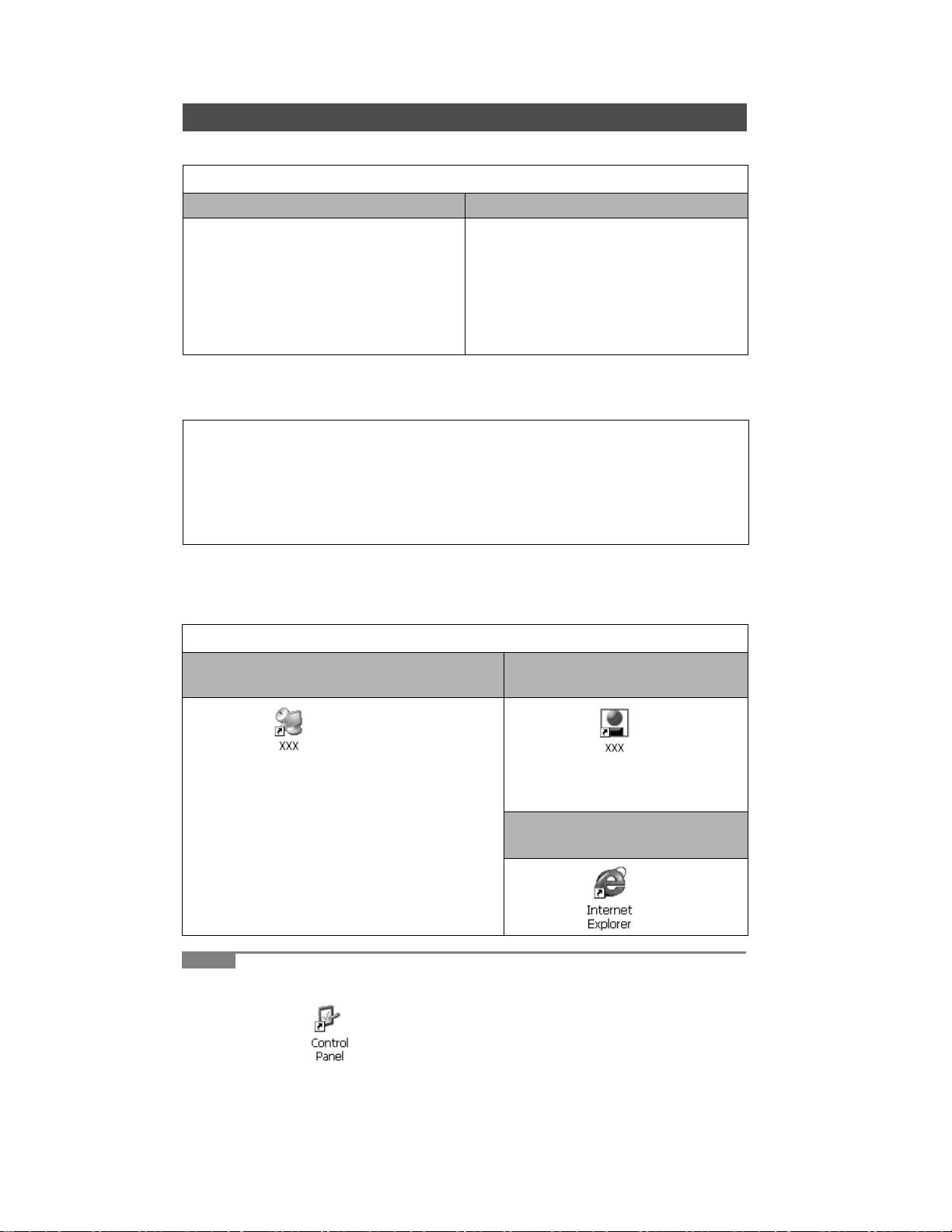
4 Starting up/Shutting Down
Starting Up
1 Turn on the wireless display.
When you log on as a Supervisor When you log on as a User
Press the power button with the USER
button pressed.
• If you do not do so, even when
you set enter the Supervisor
Password, the wireless display
will run in the User operating
environment.
2 When the [Enter Password] screen appears, enter the
password, and then tap [OK].
When you log on as a User
When the check mark is added for [Skip Password Dialog] of the [User]
tab in [Security (Supervisor)], the [Enter Password] screen is not displayed.
Press the power button.
3 Connect to the server.
When making connections with Microsoft®
Remote Desktop Connection
Double-tap
The server desktop screen will appear.
*1
The file name entered when making the
server setting will appear instead of “XXX”.
• When you do not add the check mark
for [Save my password] in “When making connections with Microsoft® Remote
Desktop Connection” step C of “Firsttime Operation” step 7
Enter the password, and then tap [OK].
NOTENOTE
When logged on as a User, the security setting screen can be displayed using
the following procedure.
① Double-tap on the desktop.
② Double-tap [Security (User)].
The following screen will appear.
*1
on the desktop.
When making connections with
Citrix® ICA® Client
*2
Double-tap
*2
The file name entered when making the server setting will appear
instead of “XXX”.
When making connections with
Microsoft
Double-tap on the desktop.
®
Internet Explorer
the desktop.
4-1
Page 13
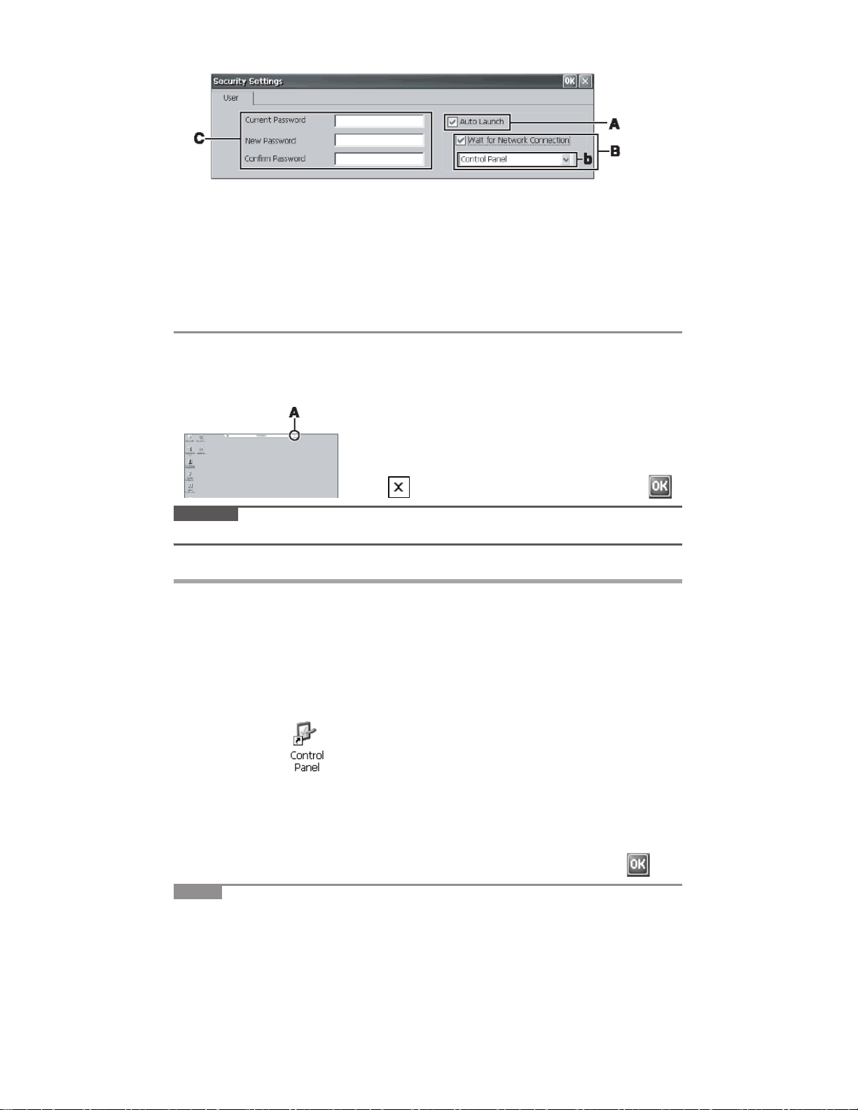
A. Auto Launch
B. Wait for Network Connection
• When the Supervisor does not
add the check mark for [Allow
Change Auto Launch] in the
[User] tab of the [Security Settings (Supervisor)] screen, [Auto
Launch] and [Wait for Network
Connection] cannot be set here.
C. Password
To set the password
• If a User Password has been set in the
[User] tab of [Security (Supervisor)]
screen, User cannot delete a password.
• If a User Password has not been set in
the [User] tab of [Security (Supervisor)]
screen, User cannot create a new
password.
When terminating the connection
Perform the following operation.
Tap [Start] - [Log Off] - [Log Off].
<Only when making connections with Microsoft
Remote Desktop Connection>
You can terminate the connection using the following
operation.
Tap (A), and when the message appears, tap .
CAUTION
If you tap [Start] - [Shut Down], the power for the server itself will be turned off.
Make the settings (only for the Supervisor)
®
When settings have been changed
Before turning off the wireless display, save (back up) the settings making reference to step
9 in “First-time Operation” .
When deleting settings
Perform the following procedure.
AADouble-tap on the desktop and double-tap [Flash Delete].
B Connect your wireless display to a power outlet.
C Tap [Delete Backup].
When the confirmation message appears, tap [Yes].
Deleting data will start.
D When the message “Backup data has been deleted.” appears, tap .
NOTENOTE
When you turn on the wireless display next time, the calibration screen will
appear.
4-2
Page 14

When returning the wireless display to its condition at the time of shipment
Perform the following procedure while the wireless display is turned off.
A Connect your wireless display to a power outlet.
B Press the power button with the keyboard button and USER button
pressed until the message “Reset the device to factory default...” appears.
When the [Enter Password] screen appears, enter the Supervisor Password and tap [OK].
C Select [Yes].
NOTENOTE
When you turn on the wireless display next time, the calibration screen will
appear.
Shutting Down (power off the wireless display)
1 Press the power button for one or two seconds until the
message “Preparing to Power off…” appears.
When shutting down forcefully, press the power button for four seconds
or longer.
4-3
Page 15
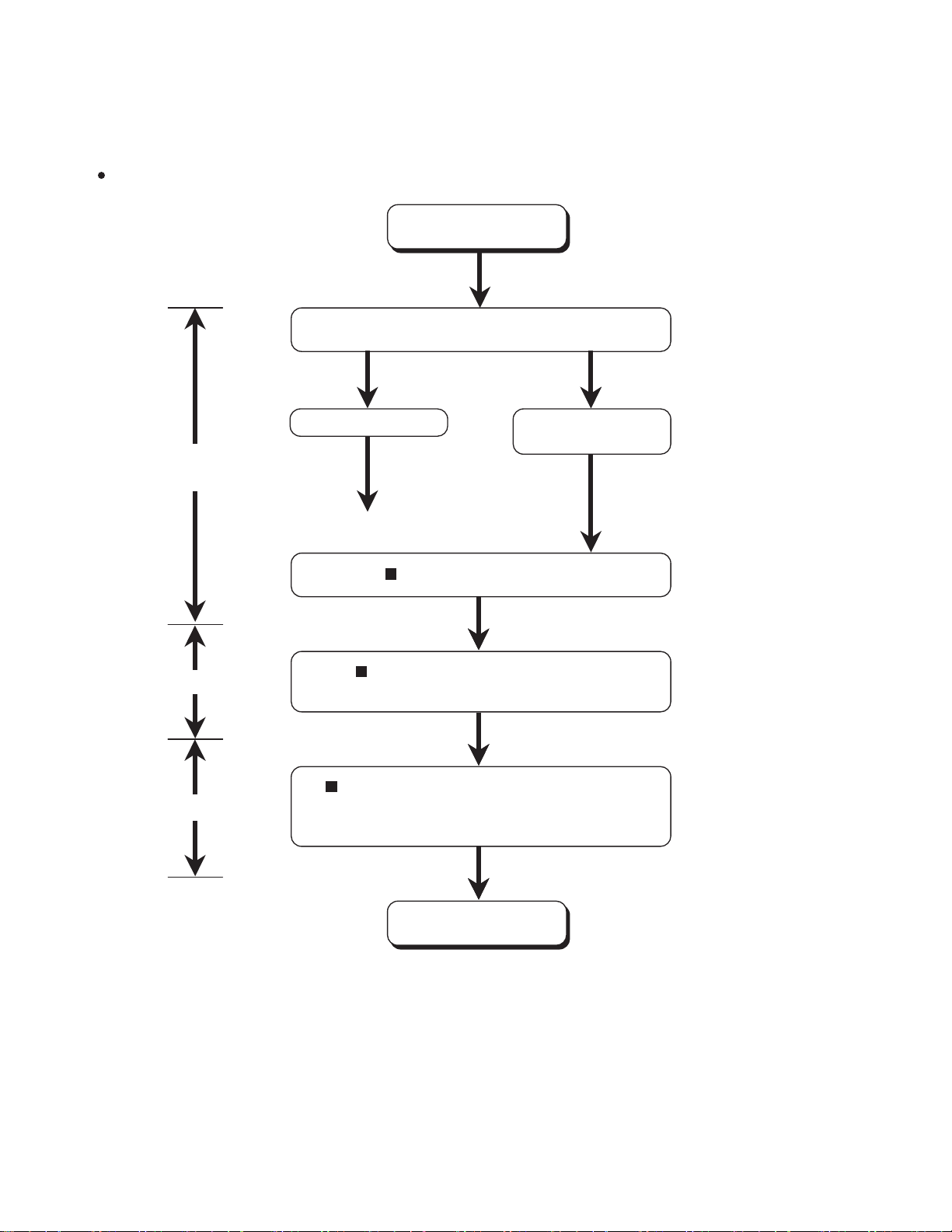
5 Diagnosis & Repair
5.1. Basic Procedures
The basic procedures for diagnosis, disassembly, and test of defective parts of a set to be repaired are summarized below.
For details, refer to relevant pages in the Service Manual.
Flow Chart
OCCURRENCE OF
TROUBLE
Insert the AC plug.
Press the Power button,
Self Test Program
Self Test Program start up.
while pressing the USER button
and the Cursor control button
at the same time.
DEFECTIVE PARTS
SORTING
REPAIR WORK
INSPECTION
NORMAL FINISH
ERROR
OCCURRENCE
OK
TROUBLESHOOTING
DISASSEMBLY PROCEDURE
Replace defective parts.
Self Test Program
After repair, make sure that the repaired
set operates properly.
TEST OK
FAULT
END OF
REPAIR WORK
5-1
Page 16
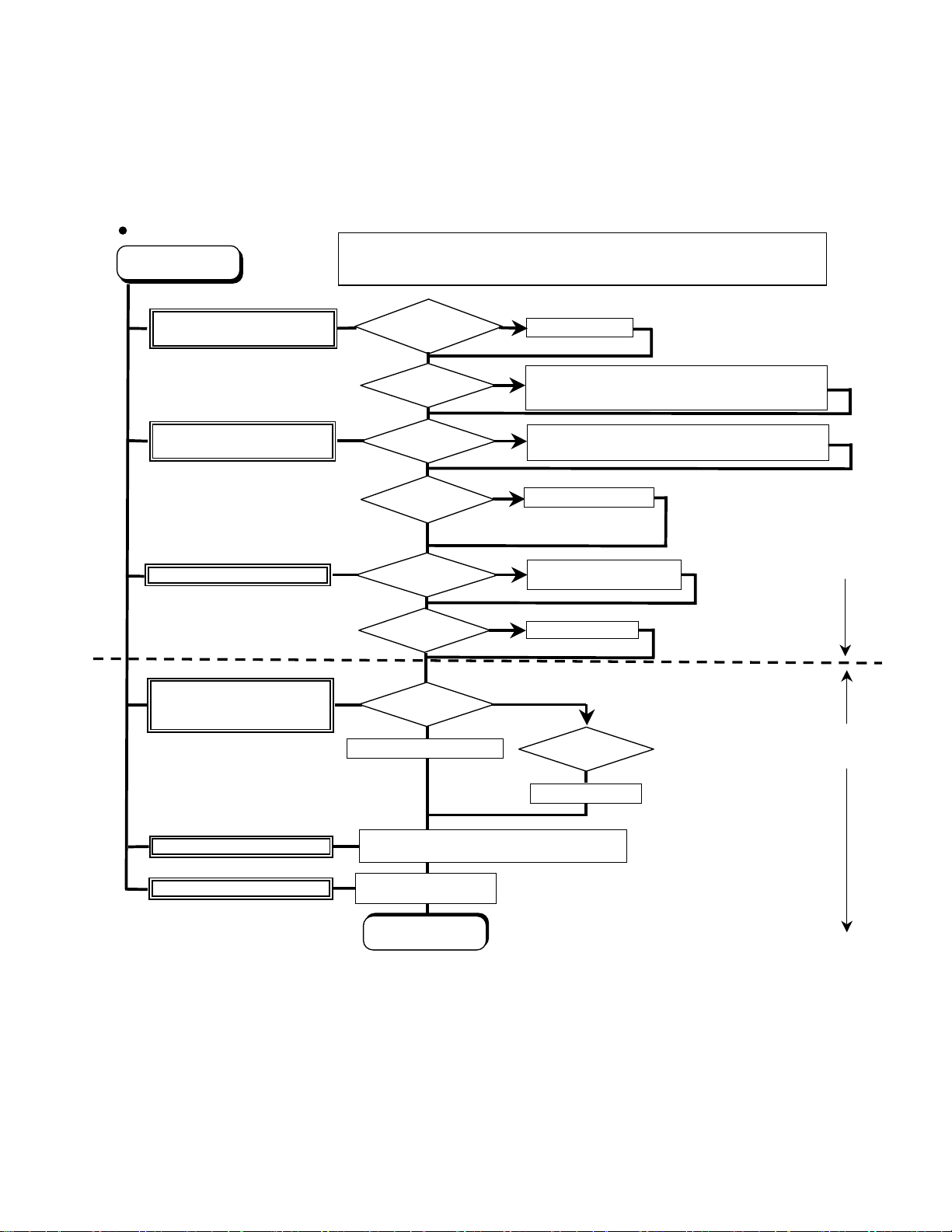
5.2. Troubleshooting
f defective.
Please take note of the following two points with regard to troubleshooting:
1. Know-how of diagnosis upon occurrence of heavy troubles, e.g. ‘Set cannot be turned ON’, ‘Set fails to start’, ‘No display on
screen’, etc.
2. Explanation of each trouble, mainly symptom of trouble in operation.
Flow Chart
START
START
Set cannot be supplied with current.
Power lamp fails to light up.
Dark display on screen.
Screen fails to display.
Failure in starting
Lines appearing on screen.
Part of block displayed
Properly on screen.
Touch screen cannot be input.
Starts but operates unstably.
Pay attention to the following points when in pursuit of the cause of a troubleshooting.
1. Peripheral apparatus connected with the set should all be removed before operation check.
2. Make sure that cables, boards, etc. are not coming off, and recheck the contact condition.
Power unit
Output voltage
NG
Replace power unit.
OK
NO
Power lamp
Board input/output
LCD back
light lighting
check
Inverter
voltage
YES
OK
Check contact condition of power input terminal. Replace i
Check SW cable continuity. Replace if defective.
Check SW board connection and contact. Replace if defective.
NG
Replace inverter board. (Check if fuse is broken).
Check inverter cable continuity. Replace if defective
NO
Replace LCD back light.
YES
operating check
NO
Replace main board
(Check fuse at power source).
YES
Result of
Selt Test Program
NG
Replace main board.
OK
LCD Unit for trial.
Replace LVDS board and cable.
Replace
OK
NG
Replace
main board
for trial.
OK
Replace main board.
Make sure of contact of Touch screen connector in use.
Replace Touch screen or main board. .
Reinstall firmware/software.
Replace main board.
Heavy trouble e.g.,
‘Set cannot be turned
ON’, ‘Set fails to start’,
‘No display on
screen’, etc.
Each kind of
trouble in
operation.
START
END
5-2
Page 17

5.3. Self Test Program
1. Introduction
This description explains Self-Test Program of this Test.
2. How to Start-up
(1) Connect the AC adaptor. ( Unless you connect the AC adaptor, the Self-Test Program
does not start. )
(2) Connect the AC adaptor. Press the USER button and Cursor Control button at the same
time, then press the Power button to turn on the computer. Self-Test Program starts
automatically.
3. Self-Test
This test is to check if the device is disconnected.
3.1. Test Items
Condut the device test in the following order.
(1) CPU Type check
(2) SDRAM march test
(3) Test register check for the source microcomputer
(4) ID check and frame buffer test for 2700G(GRAPHIC)
(5) Test register and chip ID test for LAN9118
(6) Card detection pin check and tuple information check for PCMCIA
3.1.1. CPU Type check
Check if the CPU is mounted with Intel PXA270 C5 Stepping.
3.1.2. SDRAM march test
Conduct the march test for the main-64MB and 2700G-VRAM8MB.
5-3
Page 18

3.1.3. Test register check for the source microcomputer.
Check the test register of the source microcomputer
3.1.4. ID check for 2700G
Confirm the ID of 2700G.
3.1.5. Chip ID check for LAN9118
Check the test register and chip ID of LAN9118.
3.1.6. Card detection pin check and tuple information check for PCMCIA
When you cannot obtain the tuple information, wait 0.5 second, then try to obtain the
information by calling for API. Repeat this up to 10 times. (The maximum time required: 5
seconds.)
3.2. Display during the test
The following charactors are shown during the Self-Test.
*** SELF TEST ***
Now Testing...
3.3. Test Result
When the Self Test ends normally, each test result is shown on the display. The same result
as Overall Result is shown underneath.
5-4
Page 19

If the results of all items are OK, the following display appears.
*** SELF TEST ***
CPU Type : OK
SDRAM March Test : OK
Embedded Controller : OK
2700G : OK
LAN9118 : OK
PCMCIA : OK
Overall Result : OK
If only the PCMCIA result is NG, the following display appears.
*** SELF TEST ***
CPU Type : OK
SDRAM March Test : OK
Embedded Controller : OK
2700G : OK
LAN9118 : OK
PCMCIA : NG
Overall Result : NG
After the test result is shown on the display, the program hangs.
4. How to Restart
To restart the computer, either disconnect the AC adaptor, or press and hold the power
button more than 4 seconds.
5-5
Page 20
6 Troubleshooting
Follow the instructions below when a problem has occurred. For a software problem, refer to the software’s instruction manual. If the problem persists, contact
your technical support office.
Starting Up
Cannot start up.
The power indicator or battery indicator is not lit.
Cannot turn on the
wireless display.
You have forgotten
the password.
The date and time
are incorrect.
Other startup problems.
Display
No display. The display is turned off by the power-saving function.
The screen is dark. Adjust the brightness. As you increase the brightness,
Connect the AC adaptor.
Insert a fully charged battery.
Remove the battery pack and the AC adaptor, then connect them again.
Leave it in an environment of 5 °C {41 °F} or higher
temperature for about an hour, then turn on the power
once more.
Supervisor Password or User Password: Contact your
technical support office.
Make the correct settings. Double-tap on the
desktop, and double-tap [Date/Time].
Remove all peripheral devices.
To resume, touch the LCD.
The wireless display powers off by the power-saving
function. To power on, press the power button.
battery consumption increases.
Touchscreen
The cursor does not
work.
Cannot point the
correct position
using the included
stylus.
When using the external mouse, connect it correctly.
Perform the touchscreen calibration .
6-1
Page 21

Shut Down
Cannot shut down. Press the power button for four seconds or longer to
shut down the wireless display.
Sound
No sound. Confirm the volume for [Quick Menu] or [Volume &
Sounds] in Control Panel.
Unable to hear
sound in stereo.
Wireless Communication
Playback conditions vary depending on the server.
• If you are connecting through Microsoft® Remote
Desktop Connection or a web server, you will hear
monaural sound even if the original sound is stereo.
• For playback conditions when connecting through Cit-
®
rix
Presentation Server 4.0, refer to the Citrix man-
ual for details.
Cannot connect to
network.
Connecting Peripherals
The connected keyboard and mouse
do not work.
The device connected to the serial
port does not work.
Cannot print. Check the printer connection.
Others
Check the network settings.
You may experience interference with other wireless
LAN access points.
Verify that each wireless LAN access point is set to a
different channel.
Check the keyboard and mouse connection.
Check the connection.
The device driver may not work. Refer to the instruction
manual of the device.
Do not connect two mouse devices simultaneously.
Turn on the printer.
The printer is not online.
No paper is in the printer tray or there is a paper jam.
Turn on the printer and connect it to the wireless display, and then turn on the wireless display.
No response. The screen content may not display correctly due to
poor signal quality. In such case, move to a place where
signal quality is good then make a connection.
Press the power button for four seconds or longer to
shut down the wireless display, and then press the
power button to turn it on.
6-2
Page 22
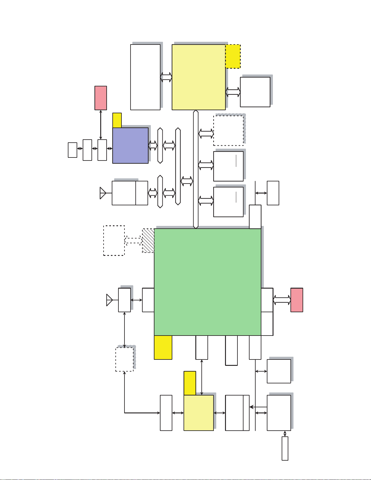
7 Block Diagram
Crystal
13.000MHz
LAN
with
10.4 inches XGA
Cradle I/F
Crystal
25MHz
FingerChip
SMSC
LAN9118
LAN
Wireless
802.11b/g
Switch
Magnetics
TachPanel and CCFL Backlight
I/O 3.3V
10/100 Base-T
CF Slot 0
16bits Bus(3.3V)
16bits Bus(3.3V)
Intel 2700G3
SN74AVCB164245
16bits Bus(3.3V)
Multimedia Accelerator
Non Stack / 384kB SRAM
32bits Bus(1.8V)
I/O 1.8V
Core 1.2V
Analog 2.5V
(1Chip)
Mobile
DiskOnChip
1.8V
(2Chip)
SDRAM
1.8V
Flash
(1Chip)
8MB
(1Chip)
x32/1.8V
SDRAM
64MB/128MB
64MB/128MB
EEPROM
S-24C04B
32MB/64MB
I2C I/F
Standard
Block Diagram
CF-08
I/O 1.8V
Bulverde
24.576MHz
with Touch screen
AC97 I/F
WM9712
controller
Microprocessor
DC-DC
MAX1586
M16C28
Battery Monitor
Battery CN
Cradle I/F
13MHz-312MHz,Core 0.85-1.3V
SD/MMC/SDIO
(Wolfson)
FL BackLight
Touch Screen
on LCD Panel
Power-MG
USB Host2
USB Host1
I2C I/F
POWER
PWM
PMC
Intel PXA270 C5
ALPS
Bluetooth
Codec
Motorola
MC145483
Serial(BT) Serial(FF )
Crystal
32.786KHz
13.000MHz
Mic/Amp/Speaker
Crystal
AC97 Codec
7-1
Page 23
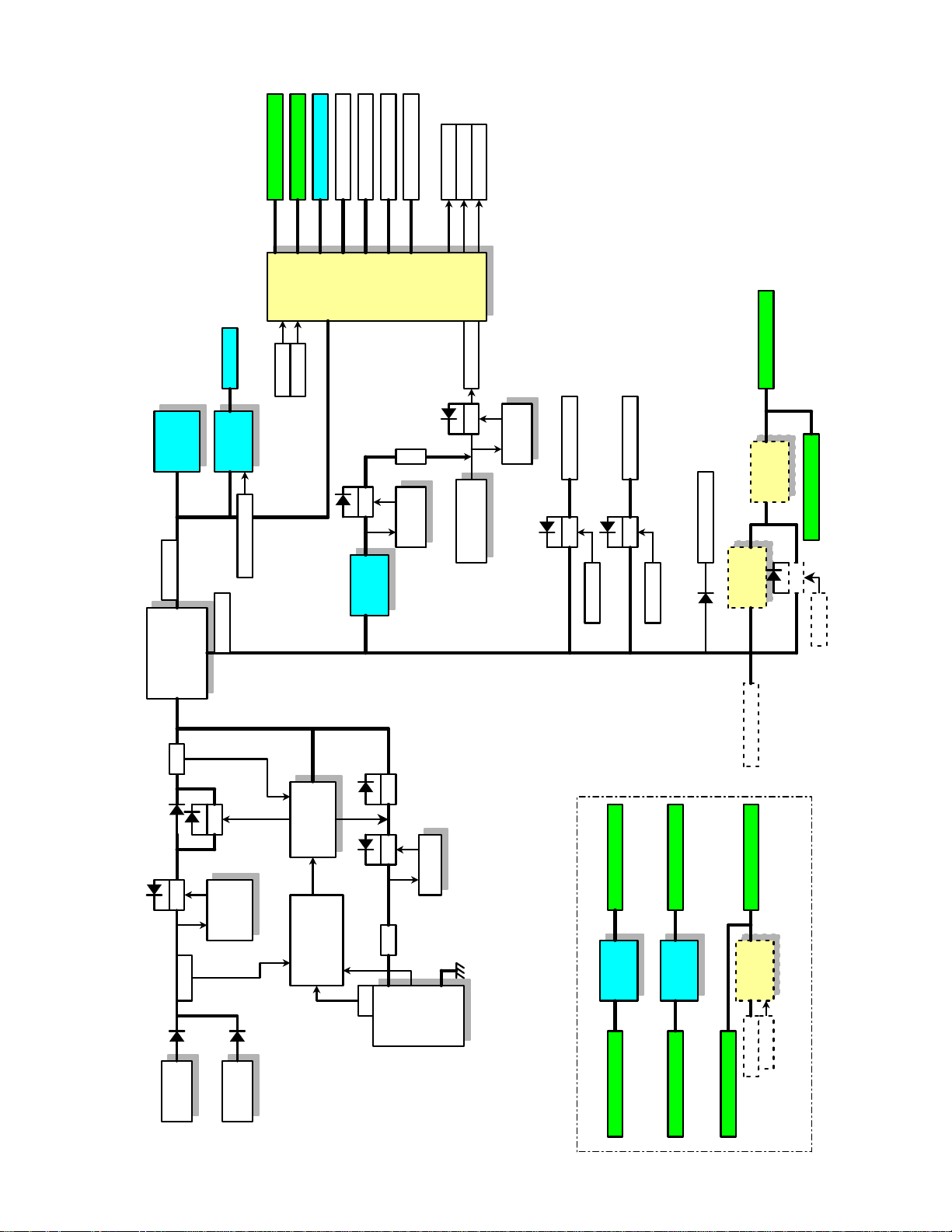
VCC_IO(3.3V)
VA3
VA3
VCC_PLL(1.3V)
VCC_MEM(1.8V)
VCC_CORE(0.8-1.3V)
VCC_USIM(3.0V)
VCC_SRAM(1.1V)
LDO
Main
DC/DC
(MAX1586)
RESET#
VCC_BATT(3.3V)
VDD_FAULT#
BATT_FAULT#
VAMP
SYS_EN
PWR_EN
LCD
Inverter
Back light
VCC_5P0V
DC/DC
(LTC3728)
R
3.3V
Voltage
Regulator
FET
AC97PWR_EN#
Voltage
VCC_3P3V
R
Voltage
Detector
3.4V
Regulator
FET
BKBT(VBK3)
FET
Voltage
Detector
WLVCC(3.3V)
Connector
Sub Battery
FET
VLAN(3.3V)
FET
CFPWR_EN
VLPWR_EN
VCC_BATT(3.3V)
BAK_1P8V(SDRAM) SYS_EN
DC/DC
(LTC3406)
VCC_MEM(1.8V)
FET
(LTC4411)
PowerPath
PWR_EN
VCC_BATT(3.3V)
FET
FET
Voltage
& OVP#
Detector
ACIN
(16V/2.5A)
AC Adapter
(16V/2.5A)
Cradle Con
Charger
(LTC4008)
FET
OVP#
V2700_Core(1.2V)
PMC
M16C28
Battery Monitor
R
Voltage
Regulator
NTC
7.4V
Battery
5200mAh
VCC_MEM(1.8V)
V2700_PLL(2.5V)
1.2V
2.5V
Voltage
Regulator
VCC_IO(3.3V)
V2700_LM(1.8V/2.5V)
DC/DC
VCC_3P3V
VCC_MEM(1.8V)
2700G Power
(LTC3406)
7-2
Page 24
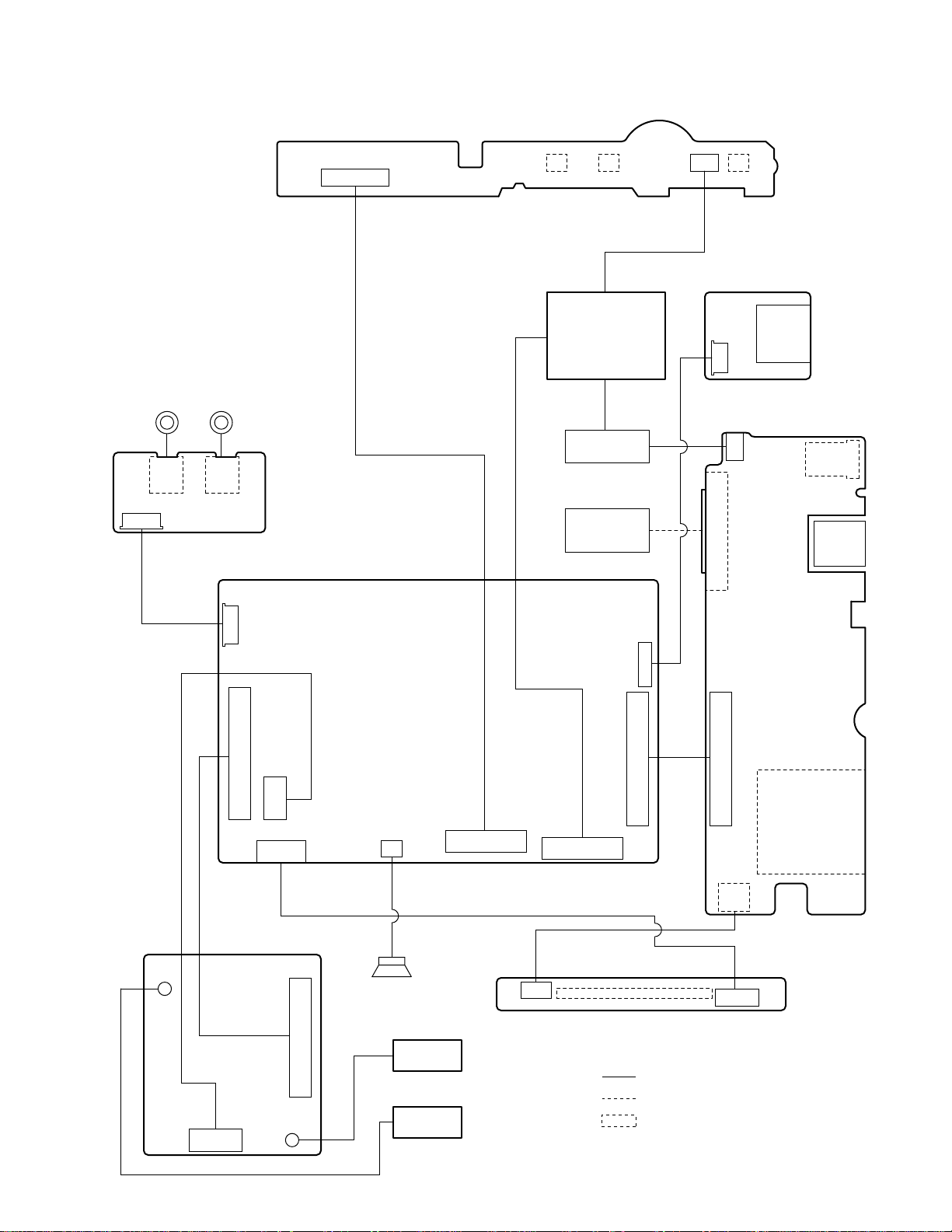
8 Wiring Connection Diagram
SW LED PCB
CN501 SW500
Microphone
CN302 CN301
CN300
AUDIO CON PCB
Headphone
CN500
SW502 SW501
LCD
INVERTER
BATTERY
PACK
USB PCB
CN400
CN401
IO POWER PCB
CN6
CN9
USB
CN7
DC-IN
CN4
LAN
CN7
WLAN PCB
CN2
CN3
CN13
CN4
CN3
CN1
MAIN PCB
CN9
SPEAKER
ANTENNA
PCB R
ANTENNA
PCB L
CN6
CN2
DOCK CON PCB
CN601
EXPANSION BUS
CN12
CN10
CN602
Connector by Cable
Direct connection by Connectors
Parts on Bottom Side
CN1
CN8
SD CARD SLOT
CN600
8-1
Page 25
9 Disassembly/Reassembly
Note:
Power off the computer. Do not shut down to the Suspend or hibernation mode.
Do not add peripherals while the computer is in the Suspend or hibernation mode; abnormal operation may result.
9.1. Disassembly Instructions
9.1.1. Preparation
Be sure to make the following preparations before disassembling.
• Shut down Windows and turn off the power.
• Disconnect the AC adaptor.
• Remove other devices if they are connected.
Attention:
• Please execute writing BIOS ID when you exchange the
Main Board.
• Parts (Sheet and rubber) etc. related various the Conductive
Cloth and Heat Spreader cannot be recycled. Use new parts.
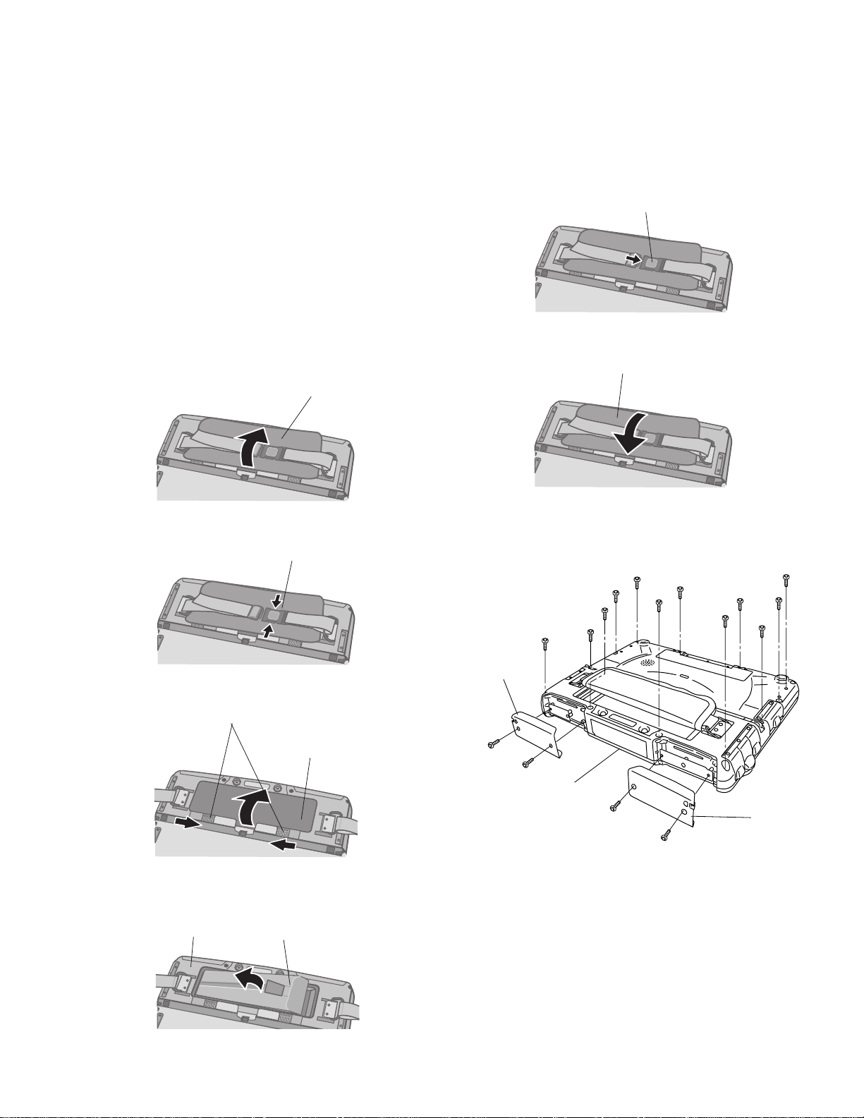
9.1.2. Removing the Battery Pack
hand strap cover
1. Open the hand strap cover.
hand strap
5. Pull the tab of the Battery Pack and remove it from the
wireless display.
hand strap
6. Attach the hand strap.
hand strap cover
7. Close the hand strap cover.
9.1.3. Removing the Display Unit
<N6>
<N6>
<N6>
<N6>
<N6>
<N6>
<N6>
<N6>
<N6>
<N6>
<N6>
<N6>
2. Remove the hand strap.
battery cover latch
battery cover
3. Slide the Battery cover latch.
4. Open and remove the Battery cover.
wireless display
battery pack
Antenna
Cover L
<N4>
<N4>
Rear Cabinet
<N4>
<N4>
Antenna
Cover R
1. Remove the two Screws <N4> and the Antenna Cover L.
2. Remove the two Screws <N4> and the Antenna Cover R.
9-1
Page 26
3. Remove the 12 Screws <N6>.
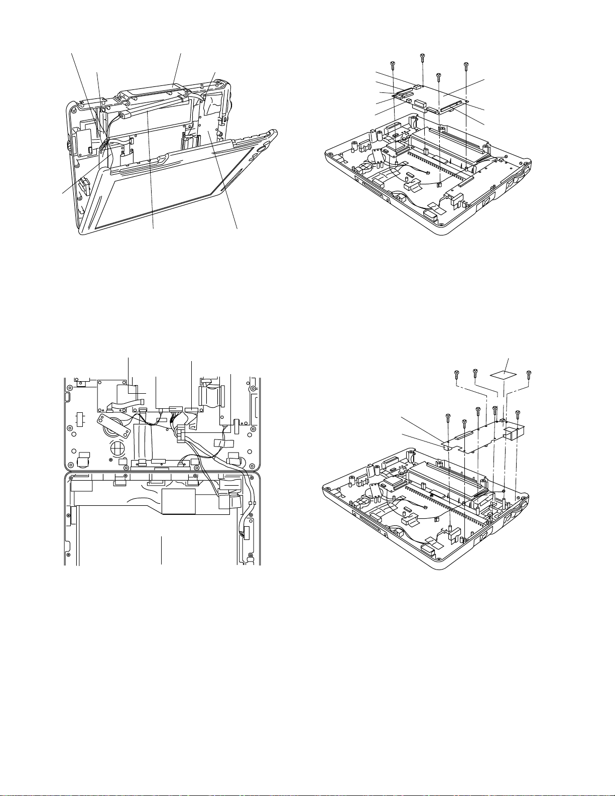
9.1.4. Removing the Main PCB
Lamp Cable Spring
Cable Holder Sheet
Cable
Rear Cabinet
Inverter
Connector(CN6)
IO Power P.C.B.
4. Remove the Cable Hold Sheet while opening the Rear
Cabinet ASS'Y slowly.
5. Remove the Cable hooked on the Lamp Cable Spring.
6. Remove both the Inverter and the Inverter Case.
7. Remove the Connector (CN6) connected to the IO Power
PCB.
8. Open the Rear Cabinet.
Main P.C.B.
Connector
(CN6)
Connector
(CN2)
Clamper
<N1>
<N1>
Connector(CN7)
Connector(CN3)
Connector(CN13)
Connector(CN4)
Connector(CN9)
<N1>
<N1>
Main P.C.B.
Connector(CN12)
Connector(CN10)
1. Disconnect the seven Cables from the Connectors
(CN3,CN4,CN7,CN9,CN10,CN12,CN13).
2. Remove the four Screws <N1>.
3. Remove the Main PCB.
Screws <N1>: XSB2+4FNL
9.1.5. Removing IO Power PCB
Edge Sheet
<N1>
<N1>
<N1>
Display
Unit
9. Remove the Clamper and the Connectors (CN2, CN6)
connected to the Main PCB.
10. Remove the Display Unit.
Screws <N4>:DXSB2+6FNL
Screws <N6>:DXYN26+J6FNL
IO Power P.C.B.
Connector(CN8)
<N1>
<N1>
<N1>
<N1>
1. Disconnect the Cable from the Connector (CN8).
2. Remove the Edge Sheet.
3. Remove the eight Screws <N1>.
4. Remove the IO Power PCB.
Screws <N1>:XSB2+4FNL
<N1>
9-2
Page 27
9.1.6. Removing the WLAN PCB
9.1.8. Removing the Speaker
Antenna Cable
<N1>
<N1>
<N1>
<N1>
A
B
Antenna Cable
B
WLAN P.C.B.
Lamp Cable Spring
A
1. Remove the two Antenna Cables.
2. Remove the four Screws <N1>.
3. Remove the Lamp Cable Spring.
4. Remove the WLAN PCB.
Screws <N1>:XSB2+4FNL
9.1.7. Removing the Audio Con PCB
Connector(CN300)
<N1>
<N1>
Edge Sheet
<K1-1-2>
<K1-1-2>
Speaker Hold Sheet
Speaker
1. Remove the two Screws <K1-1-2>.
2. Remove the Speaker Hold Sheet.
3. Remove the Speaker fixed with the two-sided tape.
Screws <K1-1-2>:XSB2+4FNL
9.1.9. Removing the USB PCB
<N1>
<N1>
Connector(CN400)
USB P.C.B.
USB Hold Plate
Audio Con P.C.B.
1. Disconnect the Cable from the Connector (CN300).
2. Remove the Edge Sheet.
3. Remove the two Screws <N1>.
4. Remove the Audio Con PCB.
Screws <N1>:XSB2+4FNL
1. Remove the two Screws <N1>.
2. Disconnect the Cable from the Connector (CN400).
3. Remove the USB Hold Plate and the USB PCB.
Screws <N1>:XSB2+4FNL
9-3
Page 28

9.1.10. Removing the WLAN L PCB
Insulation Sheet
(CN600,CN601).
Antenna Cable
WLAN L P.C.B.
<N7>
1. Remove the Insulation Sheet.
2. Remove the Screw <N7>.
3. Remove both the Antenna Cable and the WLAN L PCB.
Screw <N7>:DFHE5025XA
9.1.11. Removing the Bluetooth WLAN R
PCB
Tape
Antenna
Cable
<N3> <N3>
<N3>
<N3>
Dock Con P.C.B.
Docking P.C.B. Sheet
Base Joint Cover
<N3>
3. Remove the five screws <N3>.
4. Remove the Base Joint Cover, the Docking PCB Sheet
and the Dock Con PCB.
Screws <N3>:DXQT26+D5FNL
9.1.13. Removing the SW LED PCB
Connector(CN500)
<N2>
<N2>
SW Board Stopper Plate
<N2>
SW LED P.C.B.
Connector(CN501)
Blue tooth
<N7>
WLAN R P.C.B.
1. Remove the two tapes.
2. Remove the Screw <N7>.
3. Remove both the Antenna Cable and the Bluetooth
WLAN R PCB.
Screw <N7>:DFHE5025XA
9.1.12. Removing the Dock Con PCB
Dock Con P.C.B.
Connector(CN601)
1. Remove the FFC Hold Cushion.
2. Disconnect the two Cables from the Connectors
FFC Hold Cushion
Connector(CN600)
1. Remove the three Screws <N2>.
2. Remove the SW Board Stopper Plate.
3. Disconnect the two Cables from the Connectors
(CN500,CN501).
4. Remove the SW LED PCB.
Screws <N2>:DRSB2+5FKL
9-4
Page 29

9.1.14. Removing the LCD Unit and the
Inverter
Pet Tape
Inverter Case
1. Disconnect the Cable from the Inverter Connector.
2. Remove the Inverter with the Inverter Case.
3. Remove the Pet Tape.
TS Noise Tape
Inverter
Inverter
Connector
LCD Unit
LCD Unit
4. Remove the TS Noise Tape.
5. Remove the Cable from the Clamper.
6. Remove the LCD Unit.
Cable
Clamper
9-5
Page 30

9.2. Reassembly Instructions
9.2.1. Attention when CF-08 series is repaired
• Please execute writing BIOS ID when you exchange the Main Board.
• Parts (Sheet and rubber) etc. related various the Conductive Cloth and Heat Spreader cannot be recycled. Use new parts.
9.2.2. Setting the LCD Unit and the Inverter
1. Attach the LCD Unit.
2. Attach the TS Noise Tape.
3. Put the Cable into the Clamper.
TS Noise Tape
LCD Unit
Clamper
Cable
4. Attach the Pet Tape.
5. Connect the Cable to the Inverter connector.
Pet Tape
Inverter Case
Inverter
Inverter
Connector
LCD Unit
9-6
Page 31

■ Preparations for backlight
wide side
For appearance standard information of the LCD process,
refer to the "Common Assembly Instruction Manual".
LCD Prism Sheet
Remove the protection films. (both sides)
Handle with care.
(Avoid fingerprints or scores.)
Holder Sheet
LCD
Prism Sheet
Holder Sheet
0~0.5mm
1
Attach two sheets.
Insert into the inside the ribs.
(4 places in total)
LCD
Panel Frame
Attach in the same way as 3.
Symmetric shape
*Do not run over to the display side.
LCD
Prism Sheet
Light Guide Panel
Protection films is torn off.
(both side)
narrow side
Adhesive Tape S
Insert into the inside the ribs.
(4 places in total)
LCD Panel Frame
Do not push or press the pull base.
Reinforce Plate
Handle with care.
(Avoid fingerprints or scores.)
CCFL
narrow side
A
Insert into the inside the Hooks.
(both sides)
Safety Working
Avoid any stress when handling.
Refrecter
(Handle with care not to break.)
B
Details of "A"
0~0.5mm
Avoid
running
over the
wall.
0~0.5mm
Avoid running over the rib.
(both sides)
Do not fix the Cable at this point.
(Note) Handle with care not to damage
the light guide plate by using the Cable.
thin line: white
Avoid running over the rib
of the LCD Frame.
Reinforce Plate
thick line: pink
Tape
LCD FRAME
DBEFD Sheet
Light Guide Panel
Prism Sheet
After attaching to the light
guide plate, put pressure of
20 to 30N(2.0 to 3.0 Kgf)
on the Frame.
A
wide side
Details of "A"
Attach
Adhesive
here.
Tape L
PET Tape
0~0.5mm
*Avoid running over the display side.
(Handle 4 in the same way.)
(black side)
9-7
Insert into the inside
the Hooks.
(both sides)
Details of "B"
Insert between 5
and LCD Frame on
the opposite side
(6) as well..
Page 32

LCD Refrection Sheet
Insert after attaching 1.
Make the silver side inside.
Insert into the inside the ribs.
(4 places in total)
To avoid deflection,
do not attach 2 too
close to the Frame.
LCD
FRAME
LCD Refrection
Sheet
Holder Sheet
Positional Relation Chart for 1 and 2
LCD Refrection
Sheet
Avoid running over the rib.
(both sides)
(Running over causes moire.)
0~0.5mm
Holder Sheet
■ Assembly of the LCD
Safety Working
Notes for removing the Protection Films.
<To prevent damage to DBEF layer and
static electricity generation>
When removing the back side (inside)
Protection Film,keep the wind from the
ion-blower to the peeled side of LCD.
Then remove the Film slowly spending
more than five seconds, from LCD TAB
side on the left bottom toward along the
arrow direction.
LIGT GUIDE
PANEL
Prism Sheet
Details for attachment
0.50
~0mm
Light
Shield
Sheet A
*Remove it parallel to LCD.
OK
ionblower
NG
ionblower
Before reattaching the peeled
Protection Film to the LCD,
remove electricity.
0.5~0mm
Protection Film
LCD
Protection Film
LCD
Light Shield Sheet A
Do not bend in the
arrow direction.
*Absolutely avoid any
stress on FPC.
Handle with care.
Insert into the inside the Hooks.
(both sides)
Avoid running over AR SHEET.
Light Shield Sheet A
LCD FRAME
0~0.3mm
AR SHEET
MODULE
After removing the four sheets of the
Release Paper of the two-sided tape
on the LCD frame, then attach 1.
LCD Module
Light Shield Sheet A
Remove the Protection Films. (both sides)
Peeled Laminate Film is electric-charged.
Before reusing the Film, remove electricity.
9-8
Page 33

LCD PWB Sheet
Parts for electricity removing work
Refrect Tape
Press the Sheet along the
edge of the Reflector (Avoid floating.).
0~0.5mm
Attach here.
Lengthwise: Match to the top end of the Reflector.
Crosswise: Match to the rib of the Frame.
Standard attaching position of 1
Match to the PWC outline.
CN
Run over the end of the CN metal
(0.5 to 1 mm)
Match to the Kapton side
and attach to the Reflector
side.(Do not remove the
Release Paper other than
the Paper of the attaching
part.)
TS Noise Tape
0~1mm
Bend to the lateral side.
Pet Tape 1
A
View from A direction
LCD PWB SPACER ASSY
Insert between Board and LCD Frame.
LCD PWB SPACER ASSY
Spacer
LCD PWB Spacer
Sheet
Asymmetric shape
The form of the left and
the right isn’t symmetrical.
Holder sheet
edge standard: +0.5 mm
Spacer Sheet
Screw
0~1mm
Holder sheet
-
edge standard: +0.5 mm
-
Screw
9-9
Page 34

■ Preparations for Touchscreen
Attachment
Standard
Front Case Assy
TS Tape
Attachment
Standard
Attachment
Standard
■ Assembly of the Touchscreen
(Note)
Apply the load 20 to 30N (2.0 to 3.0 Kgf) to the Cushions.
TOUCH SCREEN ASSY
Attach the surface to the LCD Front.
TOUCH SCREEN ASSY
*Remove it parallel to the T/S.
OK
Laminate
Film
Attachment
Standard
Attachment
Standard
Attach to the center
of the display surface.
(Using the jig)
T/S
NG
Laminate
Film
T/S
<tentative measure>
After attaching the Protection Film
using jig (auto-attachment machine),
lift the film from both sides.
(like trash-catch)
Protect
Sheet
Dimensional
tolerance: +0.2
-
Fit to the stand wall and
attach to the undersurface.
LCD Side Cushion T5
edge standard:
+1mm
-
1 to 1.5 mm from
the Front Frame
TS Spacer A
2~4mm
Ensure TS spacer A, TS side
spacer and LCD FPC spacer
doesnot run over the display side.
Ensure TS side spacer does
not runover both edges of
TS glass.
TS Side Spacer
Turn the notch of the
Sheet to outside.
0.5 to 1 mm from
the Front Frame
A
Details of "A"
25–1mm
Touch Screen
LCD Side Cushion T2
Attach to
the wall.
LCD Side Cushion T5
2 to 3 mm from
the Front Frame
1 to 1.5 mm from
the Front Frame
TS Side Spacer
LCD FPC Spacer
stiffening
plate side
TS FPC
Spacer
0~0.5mm
Fit to the stand
wall and attach
to the undersurface.
Fit to the stand
wall and attach
to the undersurface.
LCD Side
Cushion T8
edge standard
+1 mm
Fit to the stand
wall and attach
to the undersurface.
LCD Side
Cushion T8
edge standard
+1 mm
9-10
Page 35

■ Assembly of the LCD Block
Shield Tape
Safety Working
0~1mm
LCD Signal Cable
edge standard: +0.5 mm
Put inside
the rib.
Match to the edge of the
Connector.
Busterade
1~3mm
0~1mm
LCD Side
Cushion T8
Attach to the
undersurface.
Frame edge
standard
+0.5mm
-
Board edge
standard
+0.5mm
-
Put inside
the rib.
edge standard: +1mm
-
Pet Tape 1
Shield Tape
LCD Block
5~6mm
Caution High
Voltage Label
LCD Side
Cushion T5
0~1mm
Attach the Conductive Cloth
to the Mg side.
(Remove the Release Paper
only of the attaching part.)
Pet Tape 1
0~3mm
Note
Caution to High Voltage
0~3mm
5~6mm 5~6mm
LCD Side Cushion Thin
After the liquid crystal block is set, attach LCD
side cushion TS and LCD side cushion thin with
their gluing sides facing downward.
1~3mm
Safety Working
When the Cable is close to the edge
(more than 4 mm than the standard position),
ensure that the Cable is not wound in other parts.
Pet Tape 1
0~3mm
5~6mm
Shield Tape
Frame edge
standard
+0.5mm
-
Board edge
standard
+0.5mm
within the rib
-
LCD Side Cushion T5
9.2.3. Setting the SW LED PCB
1. Connect the Cable to the connector (CN501) of the SW
LED PCB.
2. Attach the tape.
3. Fix the SW LED PCB and SW Board Stopper Plate using
three Screws <N2>. No1 to No3
4. Put the Cable into the Clamper.
Note:
Tighten the Screws in the numbered order (No1 to No3).
Screws <N2>:DRSB2+5FKL
Connector(CN500)
No.2
<N2>
No.3
<N2>
SW Board Stopper Plate
No.1
<N2>
SW LED P.C.B.
Connector(CN501)
9-11
Page 36

■ Assembly of the SW LED PCB
Power Button
Scroll Button
User Button
Safety Working
Lamp CN
Inverter CN Tape
Match the end.
LED Lens
Power
Button
Sheet
Attach.
Scroll
Button
Sheet
Asymmetric shape
SW Rubber
Ensure it is attached
in the notch.
Note)Avoid any stress on
the transformer of the
Inverter and the coil.
Important Parts for Safety
Inverter
Press the scroll button.
(3.0 to 4.0 Kgf)
SW
Board
in FPC direction
Place the stiffening
plate downward.
After attaching FPC, put the
Tape
Board and fix it with a tape:
CN edge standard.
SW Card Cable
Ensure the Cable does
not run over the LCD Frame.
Order of fixing
Screw-1->Screw-3
SW
Board
Stopper
Plate
Screw-2
Screw-3
Clamper
Safety Working
Pass it through
the clamper.
Screw-1
0~1mm
Lamp CN
Tape
1~2mm
0 to 1 mm
from the line
Inverter Case
After passing the case
through, attach to the back
side of the Board.
Remove the Release
Paper on the back
side and attach it,
matching it to the edge
of the case.
Match.
0 to 1 mm
from the line
Inverter
Fix Tape
Inverter
Cable
Safety Working
Pass the Cable between
the Board and rib.
Clamper
Safety Working
Pass it through the clamper.
Wrap around the Conductive Cloth on this side.
9-12
Page 37

9.2.4. Setting the Dock Con PCB
1. Fix the Docking PCB Sheet, the Base Joint Cover and the
Dock Con PCB using five Screws <N3>. No1 to No5
No.3No.4
<N3> <N3>
<N3>
No.5
Dock Con P.C.B.
Docking P.C.B. Sheet
Base Joint Cover
2. Connect the two Cables to the two connectors (CN600,
CN601) of the Dock Con PCB.
3. Attach the FFC Hold Cushion.
Note:
Tighten the Screws in the numbered order (No1 to
No5).
Screws <N3>:DXQT26+D5FNL
<N3>
No.1
Dock Con P.C.B.
Connector(CN601)
<N3>
No.2
FFC Hold Cushion
Connector(CN600)
9-13
Page 38

■ Assembly of the DOCK CON PCB
Order of fixing
Screw-1->Screw-5
Screw-4
Screw-3
Screw-5
Screw-1
Attach the Hook firmly.Ensure
the Connector Terminals of the
Sheet ( Docking PCB sheet) do
not run over.
(Attach in the arrow direction
horizontally.)
Screw-2
Match to the end of the
Connector. (0 to 1 mm)
Caption Tape
Match to the center of
Mg square hole. (– 1 mm)
Ensure the
direction is right.
Check Insert/Lock.
stiffening plate side
Cradle
Relay Card
Base Joint Cover
Docking PCB Sheet
Attach.
0~1mm
FFC Hold Cushion
Attach to the
top side of CN.
FFC
(Docking Card)
Busterade
10+1mm
Docking
PCB side
Rear Case Assy
Docking Cover Sheet
Asymmetric shape
9-14
Page 39

9.2.5. Setting the Bluetooth WLAN R PCB
1. Fix the Antenna Cable and the Bluetooth WLAN R PCB
using one Screw <N7>.
2. Fix the Antenna Cables with the two tapes.
Tape
Screw <N7>:DFHE5025XA
9.2.6. Setting the WLAN L PCB
1. Fix the Antenna Cable and the WLAN L PCB using one
Screw <N7>.
2. Fix the Antenna Cable with the Insulation Sheet.
Screw <N7>:DFHE5025XA
Antenna
Cable
<N7>
Blue tooth
WLAN R P.C.B.
Insulation Sheet
■ Assembly of the Antenna PCB
ANT Cable Packing
Press fit.
Insert until it reaches
the brim.
Screw
Antenna PCB(BT)
Screw
Antenna PCB(WLAN)
Antenna Cable
WLAN L P.C.B.
Press fit.
Insert until it reaches
the brim.
<N7>
9-15
Page 40

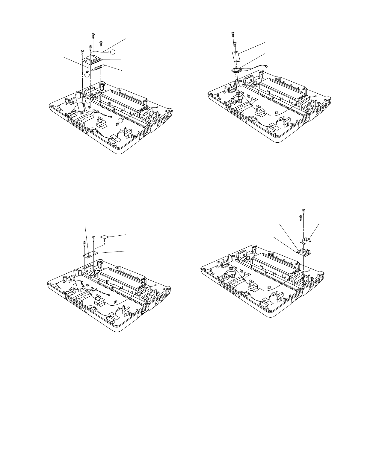
9.2.7. Setting the USB PCB
1. Fix the USB Hold Plate and the USB PCB using two
Screws <N1>.
2. Attach the Edge Sheet.
Screws <N1>:XSB2+4FNL
9.2.8. Setting the Speaker
1. Attach the Speaker.
2. Fix the Speaker Hold Sheet using two Screws <K1-1-2>.
Screws <K1-1-2>:XSB2+4FNL
<K1-1-2>
<K1-1-2>
<N1>
Connector(CN400)
USB P.C.B.
Speaker Hold Sheet
Speaker
<N1>
USB Hold Plate
9.2.9. Setting the Audio Con PCB
1. Connect the Cable to the Connector (CN300) of the Audio
Con PCB.
2. Fix the Audio Con PCB using two Screws <N1>.
3. Attach the Edge Sheet.
Screws <N1>:XSB2+4FNL
Connector(CN300)
<N1>
<N1>
Edge Sheet
Audio Con P.C.B.
9-16
Page 41

9.2.10. Setting the WLAN PCB
1. Fix the WLAN PCB and the lamp Cable Spring using four
Screws <N1>.
2. Fix the two Antenna Cables.
Screws <N1>:XSB2+4FNL
Antenna Cable
<N1>
<N1>
<N1>
<N1>
Antenna Cable
B
WLAN P.C.B.
9.2.11. Setting the IO Power PCB
1. Fix the IO Power PCB using eight Screws <N1>. No1 to
No8
2. Connect the Cable to the Connector (CN8) of the IO
Power PCB.
3. Attach the Edge Sheet.
Note:
Tighten the Screws in the numbered order (No1 to No8).
Screws <N1>:XSB2+4FNL
A
IO Power P.C.B.
Connector(CN8)
Lamp Cable Spring
B
A
No.3
<N1>
No.6
<N1>
No.7
<N1>
No.8
<N1>
No.2
<N1>
No.5
<N1>
Edge Sheet
No.1
<N1>
No.4
<N1>
9-17
Page 42

9.2.12. Setting the Main PCB
1. Connect the Cable to the Connector (CN7) of the Main
PCB.
2. Fix the Main PCB using four Screws <N1>. No1 to No4
3. Connect the Cables to the six Connectors
(CN3,CN4,CN9,CN10,CN12,CN13) of the Main PCB.
Note:
Tighten the Screws in the numbered order (No1 to No4).
Screws <N1>:XSB2+4FNL
Connector(CN7)
Connector(CN3)
Connector(CN13)
Connector(CN4)
Connector(CN9)
No.4
<N1>
No.2
<N1>
No.1
<N1>
No.3
<N1>
Main P.C.B.
Connector(CN12)
Connector(CN10)
9-18
Page 43

■ Assembly of the USB PCB, Audio Con PCB, WLAN PCB, IO Power PCB, and Main PCB
Attachment
Standard
Attach to the lateral side
in the order of a to b.
BATT CN Cover Sheet
edge –0.5mm
Screw x8
Order of fixing
Screw-1->Screw-8
Audio Con PCB
Screw
x2
Hook on the boss and tighten
together with the Board. (Fix
the short hand of the Hook.)
Direction; left opening
Lamp Cable
Spring
1~2mm
Screw
x4
WLAN PCB
1~2mm
4
Edge
Sheet
b
1
2
4
3
2
3
a
5
6
IO Power PCB
1
7
8
Screw
x4
Order of fixing
Screw-1->Screw-4
USB PCB
stiffening plate side
FFC(USB)
Check Insert/Lock.
Main PCB Hold Sheet
VGA Damper
Main PCB
Match to the
silk position.
0~1mm
within the Connector GND
Keep more than 1 mm
between the edge of FFC
folding point and the boss.
Edge Sheet
End of the CN
standard –0.5mm
USB Hold Plate
Screw
end of FFC
standard
–0.5mm
9-19
Page 44

FFC(Audio Card)
Attachment
Standard
–0.5(Board edge)
0.5mm
1
Edge Sheet
Match to the center. Match to the center.
Shield Tape
0~0.5mm
Shield Tape
FFC
(Wireless Card)
Remove half of the Release
Paper and wrap around one loop.
FFC(Audio Card)
Safety Working
Check Insert/Lock.
0~0.5mm
Busterade
Safety Working
Check Insert/Lock.
FFC
(Wireless Card)
Connect.
Ensure the correct order.
ANT Cable→FFC→Spring
BT FFC
b
Connect.
Safety Working
Check Insert/Lock.
Tape
Safety Working
Check Insert/Lock.
Connect.
Ensure the Cable does not lean to the CN
side. (Avoid coming over the A line edge
to keep the inserting room for CN. )
End of the CN
0 to 0.5 mm
Edge
Sheet
A
Attachment
Standard
–0.5(Board edge)
a
c
1~3mm
Connect.
Safety Working
Check Insert/Lock.
0~1mm
Match to the center. (–2)
*Note
Apply the load to attach. 20 to 30N (2.0 to 3.0 Kgf)
Paste Sheets firmly. 20~30N(2.0~3.0Kgf)
*
4–2mm
a
Shield
Tape
Loosen slightly not to strain.
Shield Tape
10–5mm
0~1mm
Ant.Cable
Handle FFC carefully.
Hold down the arrow
point of FFC lightly.
Tape
Remove the
Release Paper and
attach to the wall.
Power Cable
1~3mm
bc
9-20
Page 45

9.2.13. Setting the Display Unit
1. Connect the Cables to the connectors (CN2, CN6) of the
Main PCB.
2. Put the two Cables into the Clamper.
Main P.C.B.
Connector
(CN6)
Display
Unit
Connector
(CN2)
Clamper
3. Connect the Inverter Cable to the connector (CN6) of the
Power PCB as closing the Rear Cabinet.
4. Attach both the Inverter Case and the Inverter.
5. Hook the Cable on the lamp Cable Spring.
6. Attach the Cable Hold Sheet.
7. Set the LCD Unit with its face down and then close the
Rear Cabinet.
Lamp Cable Spring
Cable Holder Sheet
Cable
Rear Cabinet
Connector(CN6)
IO Power P.C.B.Inverter
9-21
Page 46

8. Fix the Rear Case ASS'Y using 12 Screws <N6>. No1 to
No12
9. Fix the Antenna Cover R using two Screws <N4>.
10. Fix the Antenna Cover L using two Screws <N4>.
Note:
Tighten the Screws in the numbered order (No1 to No12).
No.1
<N6>
No.5
<N6>
No.9
<N6>
No.12
<N6>
No.4
<N6>
No.7
<N6>
No.8
<N6>
No.6
<N6>
No.3
<N6>
No.10
<N6>
No.11
<N6>
No.2
<N6>
Screws <N4>:DXSB2+6FNL
Screws <N6>:DXYN26+J6FNL
■ Assembly of the Display unit
Safety Working
U-turn using the
pin as a guide.
Antenna
Cover L
<N4>
<N4>
Rear Cabinet
<N4>
Connect.
<N4>
Antenna
Cover R
Tape
Inside the
Pin standard
Fix with Tape not to
strain the right edge.
4~6mm
Safety Working
Safety Working
Clamper Lock
Clamp at the foot
of the Clamper.
9-22
Page 47

*Note
Ensure the Cable does not run over the Cushions (a,b,c).
Note
Avoid any stress on the transformer
and the coil.
Insert position
shape of the A boss
A
Connect.
Safety Working
Insert the cable.
Safety Working
Insert the cushions on the both sides with the "Caution to High
Voltage" label facing front until they reach the bottom while
matching the cushions to the A boss and the rib..(Top of the A boss
and the cushions on the both sides must be on the same line.)
front side
Pass between
the Pins.
A
B
Cable Hold Sheet
Safety Working
Hook the FL Cable.
Hook the Spring Hook over the cable.
Note)
Do not strain the Cable on the both
edges when removing the Inverter for
repairment.
Attach cable hold sheet to the Pin after fixing the Cable.
(B side and 1 must be on the same line oroverlaps.)
b
c
a
9-23
Page 48

9.2.14. Setting the Battery Pack
hand strap cover
battery cover latch
battery cover
battery cover latch
1. Open the hand strap cover.
hand strap
2. Remove the hand strap.
battery cover latch
battery cover
3. Slide the Battery cover latch.
4. Open and remove the Battery cover.
battery pack
6. Fit the battery cover, and then close the battery cover.
7. Slide the battery cover latch.
hand strap
8. Attach the hand strap.
hand strap cover
9. Attach the hand strap cover.
5. Firmly attach the battery pack to the connector.
9-24
Page 49

■ Assembly of the Battery Pack
*Reuse the bag used on delivery.
Battery Pack
Do not remove
through the whole
process.
Pen
Important Parts for Safety
Slide the knob to the
outside and lock firmly.
Battery Cover Assy
guide to match
the end –2 mm
Important Parts for Safety
Information Label
Allowable
displacement:
max. 1 mm
Coa Label(Win Ce)
10~15mm
Model Label
Serial Label
9-25
Page 50

Screw
Ensure the direction is right.
The side with fewer stitches is placed on the surface.
Turn the metal clasp on
both sides to the inside.
Hand Strap
Slide the knob to the
outside and lock firmly.
Screw
9-26
Page 51

10 Exploded View
N7
N7
N7
N3
N3
K8
K51
K53
E6
K42
K29
K45
E14
E16
E16
K26
K9
K10
K10
K43
K50
K18
K20
K19
K22
K7
K28
K48
K6
K5
K21
K16
E7
N7
N7
N6
N6
N6
N6
N6
N6
N6
N6
N6
N6
N7
N7
N3
N3
E8
N7
E5
E17
K15
K49
K12
N4
E2
E1
K24
K36
K46
E9
E4
K15
K15
K3
K44
K11
K39
N1
N1
N1
N1
N4
N1
E11
K11
N1
N1
N1
E18
N1
N1
N1
N1
N1
N1
K35
K23
K52
E15
K25
K26
K41
K47
K40
K23
K4
K34
N5
N5
N1
N1
K11
N1
N1
K54
K54
E7-1
E8-1
Screw tightening torque
0.2 _ 0.02N m
(2.0 _ 0.2kgf cm)
0.3 _ 0.03N m
(3.0 _ 0.3kgf cm)
0.45 _ 0.05N m
(4.5 _ 0.5kgf cm)
0.8_0.08N m
(8.0 _0.8kgf cm)
A
B
C
D
+
+
+
+
+
+
+
A
A
A
A
A
A
A
A
A
A
A
A
A
A
C
C
C
B
N3
B
B
A
C
C
C
C
C
C
D
A
A
C
A
A
A
D
B
A
A
A
A
A
A
C
CF-08TX1A1M
10-1
Page 52

K1
K1-3
K1-7
K1-8
K1-6
K1-1
K1-2
K1-9
K1-1-1
A
K1-1-2
K1-1-5
K1-1-7
Capton tape
(10 25)
K1-1-4
K1-1-6
K1-3
K1-10
K1-5
K1-4
K1-1-13
K1-6
Capton tape
(10 25)
K1-7
K1-3
K1-7
K1-8
K1-1-12
K1-1-3
K1-1-8
K1-1-14
K1-1-12
K1-1-10
K1-1-9
K1-1-11
Screw tightening torque
A
0.2 _ 0.02N m
+
(2.0 _ 0.2kgf cm)
+
CF-08TX1A1M
10-2
Page 53

K200-1
K200-4
K200-3
K200-2
K200-2-6-1
K200-6
K200-3
K200-4
K37
K200-4
K200-5
K200-3
K37
K200-2-1
K200-4
K200-3
K200-2-6
K200
K31
K32
K17
E3
A
A
K11
A
E13
K33
K30
K2
N2N2
A
K38
K200-2-5
E19-1
K201
K200-2-4
E19-1-3
E19-3
K201
E19-1-2
E20
K200-2-5
K200-2-2
E19-2
E19
K200-2-3
E19-1-1
Screw tightening torque
A
0.2 _ 0.02N m
+
(2.0 _ 0.2kgf cm)
+
K14
E10
K13
K27
E12
10-3
CF-08TX1A1M
Page 54

11 Replacement Parts List
Note: Important Safety Notice
Components identified by mark have special characteristics important for safety.
When replacing any of these components, use only manufacturer's specified parts.
CF-08TX1A1M
REF.NO. and AREA PART NO. DESCRIPTION Q'TY
Main Block Unit
E1 DL3UP1486AAA PCB, MAIN RTL 1
E2 DL3U11487AAA PCB, IO POWER RTL 1
E3 DL3U21487AAA PCB, SW LED RTL 1
E4 DL3U31487AAA PCB, AUDIO CON RTL 1
E5 DL3U41487AAA PCB, USB RTL 1
E6 DL3U51487AAA PCB, DOCK CON RTL 1
E7 DL3U11489AAA PCB, BLUETOOTH WLAN R RTL 1
E7-1 DFJS1016ZA WLAN/BT CABLE R 1
E8 DL3U21489AAA PCB, WLAN L RTL 1
E8-1 DFJS899ZA ANTENNA CABLE L 1
E9 DL3UP1488AAA PCB, WLAN RTL 1
E10 N0GB1J000018 INVERTER 1
E11 DFJS1012ZA POWER CABLE 1
E12 DFJS1014ZA INVERTER CABLE 1
E13 DFJS1015YA SWITCH CABLE 1
E14 DFJK10T068DB FP FFC 1
E15 DFJK16T078DB DOCKING FFC 1
E16 DFJK50T043DB LAN/POWER FFC 2
E17 DFJK9015ZA USB FFC 1
E18 DFJK9019ZA BT FFC 1
E19 DFWV08A0085 LCD ASS'Y 1
E19-1 DL3DW0181AAA LCD ASS'Y 1
E19-1-1 A2CA00000066 BACK LIGHT 1
E19-1-2 DFHM0290ZA REFLECTION ANGLE 1
E19-1-3 DFQT9863ZA LCD ATTENTION LABEL 1
E19-2 DFHE0995YA TS NOISE SHEET 1
E19-3 DFHE0646ZA BUSTERADE 1
E20 DFJS1011ZA LCD CABLE 1
Accessories
A1 CF-AA1623AM6 AC ADAPTOR 1
A2 N4HULSA00003 BATTERY PACK 1
A3 K2CG3DR00003 AC CABLE 1
A4 DFQX5591ZA MANUAL 1
A5 DFME0148ZA TETHER 1
A6 DFHS9017ZA TOUCH PANEL CLOTH ASS'Y 1
Packing Material
P1 DFPK1187ZA PACKING CASE 1
P2 DFPN0828ZB CUSHION B 2
P3 DFPN0832ZA CUSHION T 2
P4 DFPK1037YA ACCESSORY BOX 1
P5 DFPE0830ZA HOLDER 1
Mechanical Parts
K1 DFWV80C0505 REAR CABINET ASS'Y 1
K1-1 DFKE9081YA-0 REAR CASE ASS'Y 1
K1-1-1 L0AA02A00069 SPEAKER 1
K1-1-2 XSB2+4FNL SCREW 2
K1-1-3 DFHG898ZA BATTERY SPACER 1
K1-1-4 DFHP7230ZA SPEAKER BASE SHEET UPPER 1
K1-1-5 DFHP7258ZA SPEAKER TAPE 1
K1-1-6 DFHR3C72ZA SPEAKER BASE LOWER SHEET 1
11-1
Page 55

K1-1-7 DFHR3C73ZA SPEAKER HOLD SHEET 1
K1-1-8 DFHR3C75ZA BATTERY BOTTOM BLIND SHEET 1
K1-1-9 DFHR3C76YA USB SHEET 1
K1-1-10 DFHR3C78ZA LAN SHEET 1
K1-1-11 DFHR3C79ZA SD SHEET 1
K1-1-12 DFHR3C80ZA PEN HOLD SHEET 2
K1-1-13 DFHR3C82ZA MAIN PCB INS. SHEET 1
K1-1-14 DFQT9976ZA-0 SD LED SIGN LABEL 1
K1-2 DFMD1197ZA KENSINGTON PLATE 1
K1-3 DFMC0867ZA EMI CLOTH 3
K1-4 DFMY3232ZA HEAT RADIATION PLATE 1
K1-5 DFHG894XA LCD REAR CUSHION T3L 1
K1-6 DFHG895ZA LCD REAR CUSHION T3S 2
K1-7 DFHG896ZA LCD REAR CUSHION T6L 3
K1-8 DFHG897ZA LCD REAR CUSHION T6M 2
K1-9 DRQT2+I35FKL SCREW 1
K1-10 DFHR1108ZA LCD REAR CLAMPER 1
K2 DFMD2179ZA SW BOARD PLATE 1
K3 DFMD3126ZA USB HOLD PLATE 1
K4 DFMD4061ZA-0 CARD READER BLIND PLATE 1
K5 DFMD4062ZA-0 AUDIO COVER PLATE 1
K6 DFMD4063ZA-0 DC/USB COVER PLATE 1
K7 DFMD4064ZA-0 SD COVER PLATE 1
K8 DFMD4065ZA BATTERY MAGNET COVER PLATE 1
K9 DFMC0866ZA AUDIO EMI SHEET 1
K10 DFMC0867ZA EMI CLOTH 2
K11 DFMX0734ZA PROTECT SHEET 5
K12 DFMX1236ZA IO BOARD EDGE SHEET 1
K13 DFMX1237YA CN FIX TAPE 2
K14 DFMX9011ZA INVERTER CASE ASS'Y 1
K15 DFHG1331ZA SHIELD SHEET(LAN JACK) 3
K16 DFHG1714ZA ANT CABLE PACKING 1
K17 DFHG1841XA SW BOARD RUBBER 1
K18 DFHG1842ZA-0 DC COVER 1
K19 DFHG1843ZA-0 USB COVER 1
K20 DFHG1844ZA-0 LAN COVER 1
K21 DFHG1845ZA-0 AUDIO COVER 1
K22 DFHG1846ZA-0 SD COVER 1
K23 DFHG370ZA-1 FOOT RUBBER 2
K24 DFHG900ZA VGA DAMPER 1
K25 DFHE0465ZA EMI SHEET 5 1
K26 DFHE0646ZA BUSTERADE 2
K27 DFHP7168ZA INVERTER TAPE 1
K28 DFKH1019ZA-0 HANDY STRAP 1
K29 DFKE9085ZA-0 BATTERY COVER ASS'Y 1
K30 DFGL0152ZA-0 LED LENS 1
K31 DFBC0317ZA-0 POWER BUTTON 1
K32 DFBC0318ZA-0 USER BUTTON 2
K33 DFBC0319ZA-0 SCROLL BUTTON 1
K34 DFBD9007ZA-0 BATTERY LOCK ASS'Y R 1
K35 DFBD9008ZA-0 BATTERY LOCK ASS'Y L 1
K36 DFHR1109ZA LAMP CABLE SPRING 1
K37 DFHR1110ZA LCD SW CABLE CLAMPER 2
K38 DFHR3159ZA TOP CASE SHEET 1
K39 DFHR3636ZA CABLE HOLD SHEET 1
K40 DFHR3741ZA FFC CN STOPPER 1
K41 DFHR3C41YA DOCKING PCB SHEET 1
K42 DFHR3C42YA DOCKING COVER SHEET 1
11-2
Page 56

K43 DFHR3C43ZA-0 CARD BLIND SHEET 1
K44 DFHR3C74ZA BATTERY CN COVER SHEET 1
K45 DFHR3C77YA AUDIO SHEET 1
K46 DFHR3C81YA MAIN PCB HOLD SHEET 1
K47 DFHR3E39ZA CAPTON TAPE 1
K48 DFHR6207ZA PEN 1
K49 DFHR6224ZA-0 ANTENNA COVER L 1
K50 DFHR6225ZA-0 ANTENNA COVER R 1
K51 DFHR6226ZA-0 PEN COVER 1
K52 DFHR6227ZA-0 BASE JOINT COVER 1
K53 DFGT1079ZA-0 INFORMATION LABEL 1
K54 DFHG1714XA ANT CABLE PACKING 2
K200 DFWV80A0359 FRONT CABINET ASS'Y 1
K200-1 DFKF9032ZA-0 FRONT CASE ASS'Y 1
K200-2 DFWV84A0270 TOUCH SCREEN PANEL KIT 1
K200-2-1 DFHP7229ZA TS TAPE 1
K200-2-2 DFHR3476ZA TS SPACER A 1
K200-2-3 DFHR3630ZA TS FPC SPACER 1
K200-2-4 DFHR3D66ZA TS SPACER L 1
K200-2-5 DFHR3D70ZA TS SIDE SPACER 2
K200-2-6 DL3DV0181AAA TS PANEL ASS'Y 1
K200-2-6-1 N2BAAYY00007 TOUCH SCREEN 1
K200-3 DFHG891YA LCD SIDE CUSHION T8 4
K200-4 DFHG892YA LCD SIDE CUSHION T5 4
K200-5 DFHG893ZA LCD SIDE CUSHION T2 1
K200-6 DFHG899ZA LCD SIDE DAMPER THIN 2
K201 DFMC0867ZA EMI CLOTH 3
N1 XSB2+4FNL SCREW 24
N2 DRSB2+5FKL SCREW 3
N3 DXQT26+D5FNL SCREW 9
N4 DXSB2+6FNL SCREW 4
N5 DXSN4+6FNL SCREW 2
N6 DXYN26+J6FNL SCREW 12
N7 DFHE5025XA SCREW 13
11-3
Page 57

Replacement Parts List
A
Note: Important Safety Notice
Components identified by mark have special characteristics important for safety.
When replacing any of these components use only manufacturer's specified parts.
CF-08TX1A1M
REF. NO and ARE
MAIN PCB
C 1 F1G1E103A062 CAPACITOR, 25V, 0.01µF 25
C10
C50
C 150
C 151
C 164
C 169
C 171
C 187
C 188
C 207
C 245
C 247
C 250
C 266
C 278
C 279
C 280
C 311
C 312
C 313
C 314
C 324
C 325
C 326
C 5 F1G1H1R0A543 CAPACITOR, 50V, 1pF 1
C 7 F1G1A104A014 CAPACITOR, 10V, 0.1µF 152
C8
C9
C15
C16
C17
C18
C19
C20
C21
C22
C23
C24
C25
C26
PART NO. DESCRIPTION
Q'TY
11-4
Page 58

C27
C28
C29
C30
C31
C32
C33
C34
C35
C36
C37
C38
C39
C40
C41
C42
C43
C44
C49
C52
C53
C55
C56
C57
C65
C66
C67
C68
C69
C70
C71
C74
C75
C81
C82
C83
C84
C85
C86
C87
C88
C89
C90
C91
C92
C93
C94
C95
C96
C97
11-5
Page 59

C98
C 102
C 103
C 104
C 105
C 106
C 107
C 108
C 109
C 110
C 111
C 112
C 113
C 114
C 115
C 116
C 117
C 118
C 119
C 120
C 121
C 122
C 125
C 126
C 127
C 138
C 139
C 140
C 141
C 142
C 147
C 148
C 152
C 163
C 170
C 172
C 173
C 175
C 176
C 177
C 178
C 179
C 180
C 181
C 182
C 184
C 186
C 215
C 226
C 230
11-6
Page 60

C 232
C 233
C 234
C 239
C 241
C 265
C 274
C 276
C 277
C 281
C 282
C 283
C 284
C 285
C 286
C 287
C 288
C 293
C 294
C 295
C 296
C 297
C 298
C 299
C 300
C 301
C 303
C 304
C 306
C 310
C 315
C 316
C 317
C 318
C 319
C 320
C 323
C 11 F1G1H102A496 CAPACITOR, 50V, 1000pF 3
C 216
C 217
C 45 F1G1H680A451 CAPACITOR, 50V, 68pF 4
C46
C47
C48
C 54 F1H1A1050015 CAPACITOR, 10V, 1µF 17
C 129
C 131
C 132
C 133
C 220
11-7
Page 61

C 221
C 229
C 231
C 235
C 257
C 258
C 259
C 262
C 263
C 268
C 308
C 100 F1J0J1060004 CAPACITOR, 6.3V, 10µF 23
C 101
C 124
C 135
C 137
C 149
C 174
C 183
C 190
C 191
C 236
C 237
C 238
C 242
C 246
C 248
C 252
C 254
C 255
C 256
C 302
C 305
C 307
C 165 F1G1H8R0A452 CAPACITOR, 50V, 8pF 2
C 166
C 167 F1G1E682A062 CAPACITOR, 25V, 6800pF 2
C 168
C 189 F1G1C223A004 CAPACITOR, 16V, 0.022µF 1
C 193 F1H0J1050022 CAPACITOR, 6.3V, 1µF 3
C 194
C 222
C 210 F1G0J224A001 CAPACITOR, 6.3V, 0.22µF 5
C 211
C 214
C 244
C 249
C 223 EEFCD0J470ER CAPACITOR, 6.3V, 47µF 5
C 224
C 225
11-8
Page 62

C 240
C 243
C 227 F1G1H100A452 CAPACITOR, 50V, 10pF 2
C 228
C 251 F1J0J226A048 CAPACITOR, 6.3V, 22µF 6
C 253
C 269
C 336
C 337
C 338
C 260 F1G1H331A450 CAPACITOR, 50V, 330pF 3
C 261
C 264
C 267 F1G1H332A496 CAPACITOR, 50V, 3300pF 1
C 270 EEFUD0J101ER CAPACITOR, 6.3V, 100µF 2
C 271
C 330 F1L1H100A072 CAPACITOR, 50V, 10pF 2
C 331
CN 1 K1KA10BA0014 CONNECTOR 1
CN 2 K1KA14BA0098 CONNECTOR 1
CN 3 K1MN50AA0018 CONNECTOR 2
CN 10
CN 4 K1MN16BA0059 CONNECTOR 1
CN 6 K1KA30BA0060 CONNECTOR 1
CN 7 K1MN10B00146 CONNECTOR 1
CN 9 K1KA02BA0085 CONNECTOR 1
CN 12 K1MN08AA0068 CONNECTOR 1
CN 13 K1MN12AA0018 CONNECTOR 1
D 1 B0KB00000044 DIODE 5
D2
D7
D8
D9
D 5 B0JCMD000014 DIODE 2
D6
FL 1 J0MAB0000169 FILTER 2
FL 2
FL 3 J0MAB0000116 FILTER 2
FL 4
IC 1 C2GBC0000268 IC, CPU 1
IC 4 C0EBE0000459 IC 2
IC 36
IC 5 C0EBD0000313 IC 1
IC 6 C0JBAZ002067 IC, LOGIC 2
IC 53
IC 8 C1CB00002385 IC, CONTROLLER 1
IC 9 C0JBAB000619 IC, GATE LOGIC 3
IC 21
IC 29
IC 10 C3ABRY000010 IC, SDRAM 2
11-9
Page 63

IC 11
IC 15 C3FBRY000001 IC, FLASH MEMORY 1
IC 16 C3ABPY000009 IC, SDRAM 1
IC 19 C0CBCAC00161 IC 1
IC 22 C0JBCZ000523 IC 1
IC 23 C0JBAZ002770 IC, LOGIC 1
IC 26 C0JBAZ002758 IC, LOGIC 1
IC 27 C0JBAZ002239 IC, GATE LOGIC 4
IC 34
IC 35
IC 37
IC 28 C0ZBZ0001023 IC 2
IC 30
IC 31 C0JBAA000350 IC, LOGIC 1
IC 32 C0JBAC000338 IC, GATE LOGIC 1
IC 39 C1CB00002054 IC, LAN CONTROLLER 1
IC 42 C1BB00000895 IC, AC97 CODEC 1
IC 43 C0CBCBC00130 IC, REGURATOR 1
IC 44 C1BB00000873 IC, AUDIO AMP 1
IC 45 C0DBAGG00014 IC 1
IC 49 C1CB00002478 IC, LAN SWITCH 1
IC 50 C0CBAAC00163 IC 1
IC 51 C3EBEC000061 IC, EEPROM 1
L 1 J0JDC0000045 INDUCTOR 4
L2
L14
L15
L 3 J0JHC0000074 INDUCTOR 3
L5
L6
L 12 DDB5Z024E-L INDUCTOR 1
L 13 J0MAB0000174 INDUCTOR 1
L 16 G1C3R3MA0077 INDUCTOR 2
L18
L 17 G1C4R7MA0077 INDUCTOR 1
Q 1 B1CFGD000004 TRANSISTOR 4
Q3
Q4
Q26
Q 8 B1DHDC000028 TRANSISTOR 6
Q10
Q22
Q24
Q28
Q29
Q 9 UNR9213J0L TRANSISTOR 6
Q23
Q25
Q30
Q31
11-10
Page 64

Q44
Q 27 UNR9113J0L TRANSISTOR 3
Q33
Q36
Q 34 XP0421300L TRANSISTOR 3
Q35
Q38
R 1 ERJ2GEJ473X RESISTOR, 1/16W, 47KΩ 21
R28
R29
R30
R31
R32
R33
R36
R38
R 168
R 171
R 177
R 178
R 179
R 310
R 311
R 312
R 353
R 354
R 355
R 356
R 2 ERJ2GEJ102X RESISTOR, 1/16W, 1K Ω 9
R62
R 172
R 174
R 241
R 242
R 307
R 308
R 309
R 5 ERJ2GE0R00X RESISTOR, 1/16W, 0Ω 22
R6
R50
R51
R72
R 115
R 116
R 118
R 119
R 120
R 180
R 200
R 234
11-11
Page 65

R 265
R 275
R 277
R 279
R 283
R 284
R 292
R 325
R 327
R 7 ERJ2GEJ103X RESISTOR, 1/16W, 10KΩ 11
R8
R9
R24
R37
R43
R 243
R 244
R 253
R 255
R 256
R 10 ERJ2GEJ100X RESISTOR, 1/16W, 10Ω 16
R11
R12
R13
R14
R15
R16
R17
R18
R19
R20
R21
R27
R46
R 187
R 331
R 22 ERJ2GEJ122X RESISTOR, 1/16W, 1.2KΩ 9
R23
R44
R45
R 195
R 196
R 197
R 199
R 305
R 25 ERJ2GEJ105X RESISTOR, 1/16W, 1MΩ 3
R 191
R 233
R 34 ERJ2GEJ330X RESISTOR, 1/16W, 33Ω 9
R 220
11-12
Page 66

R 221
R 222
R 223
R 357
R 358
R 359
R 360
R 35 ERJ2GEJ104X RESISTOR, 1/16W, 100KΩ 58
R49
R77
R78
R89
R92
R94
R96
R98
R99
R 101
R 102
R 103
R 108
R 111
R 112
R 113
R 114
R 117
R 133
R 134
R 135
R 136
R 145
R 146
R 147
R 149
R 150
R 151
R 152
R 153
R 155
R 156
R 157
R 160
R 161
R 164
R 169
R 183
R 185
R 188
R 189
R 219
11-13
Page 67

R 224
R 235
R 245
R 252
R 259
R 260
R 261
R 262
R 287
R 319
R 320
R 341
R 344
R 345
R 346
R 39 ERJ3GEY0R00V RESISTOR, 1/16W, 0Ω 18
R42
R53
R70
R74
R 107
R 123
R 124
R 127
R 129
R 132
R 143
R 269
R 270
R 272
R 273
R 285
R 286
R 54 ERJ2GEJ150X RESISTOR, 1/16W, 15Ω 4
R55
R58
R59
R 56 ERJ2GEJ153X RESISTOR, 1/16W, 15KΩ 4
R57
R 137
R 139
R 141 ERJ6GEY0R00V RESISTOR, 1/10W, 0 Ω 6
R 142
R 263
R 267
R 271
R 295
R 162 ERJ2GEJ475X RESISTOR, 1/16W, 4.7MΩ 1
R 170 ERJ2GEJ271X RESISTOR, 1/16W, 270Ω 8
R 347
11-14
Page 68

R 361
R 362
R 363
R 364
R 365
R 366
R 204 ERJ2RKF49R9X RESISTOR, 1/16W, 49.9Ω 4
R 205
R 206
R 207
R 210 ERJ3EKF1202V RESISTOR, 1/10W, 12K Ω 1
R 211 ERJ3EKF1242V RESISTOR, 1/10W, 12.4K Ω 1
R 236 ERJ2GEJ101X RESISTOR, 1/16W, 100Ω 9
R 237
R 238
R 239
R 240
R 290
R 291
R 367
R 368
R 246 ERJ2GEJ472X RESISTOR, 1/16W, 4.7KΩ 3
R 247
R 251
R 248 ERJ2RHD273X RESISTOR, 1/16W, 27KΩ 1
R 257 ERJ2RKF1002X RESISTOR, 1/16W, 10KΩ 1
R 274 ERJ2GEJ224X RESISTOR, 1/16W, 220KΩ 3
R 278
R 282
RA 1 D1HG1008A001 RESISTOR ARRAY 6
RA 2
RA 3
RA 4
RA 5
RA 6
X 1 H0J130500003 OSCILLATOR, 13MHz 1
X 2 H0J327200113 OSCILLATOR, 32.768KHz 1
X 4 H0J250500025 OSCILLATOR, 25MHz 1
X 5 H0J245500061 OSCILLATOR, 24.576MHz 1
IO POWER PCB
C 3 F1G1A104A014 CAPACITOR, 10V, 0.1µF 15
C7
C13
C49
C50
C51
C53
C54
C57
C59
11-15
Page 69

C60
C61
C62
C68
C73
C 4 F1J0J1060004 CAPACITOR, 6.3V, 10µF 6
C5
C44
C55
C56
C58
C 6 F1G1E103A062 CAPACITOR, 25V, 0.01µF 7
C11
C47
C48
C69
C70
C71
C 8 F1H1H104A748 CAPACITOR, 50V, 0.1µF 11
C10
C16
C19
C20
C21
C26
C30
C33
C45
C65
C 9 F1J1E105A009 CAPACITOR, 25V, 1µF 1
C 12 F1H1A1050015 CAPACITOR, 10V, 1µF 3
C22
C72
C 15 F1L1E106A017 CAPACITOR, 25V, 10µF 6
C18
C23
C24
C29
C42
C 25 F1G1H152A450 CAPACITOR, 50V, 1500pF 1
C 27 EEFUD0J101ER CAPACITOR, 6.3V, 100µF 2
C28
C 31 F1H1H103A748 CAPACITOR, 50V, 0.01µF 2
C40
C 32 F1G1H1010005 CAPACITOR, 50V, 100pF 3
C41
C46
C 34 F1G1H102A496 CAPACITOR, 50V, 1000pF 3
C39
C64
11-16
Page 70

C 35 F1G1H220A542 CAPACITOR, 50V, 22pF 4
C38
C76
C79
C 36 F1G1H221A450 CAPACITOR, 50V, 220pF 2
C37
C 52 F1H0J1050022 CAPACITOR, 6.3V, 1µF 1
C 63 F1G1A683A014 CAPACITOR, 10V, 0.068µF 1
C 66 F1L3D102A012 CAPACITOR, 2000V, 1000pF 2
C67
C 74 F1G1H100A452 CAPACITOR, 50V, 10pF 4
C75
C77
C78
CN 1 K1MN50B00046 CONNECTOR 1
CN 3 K1NA09E00076 CONNECTOR, SD MEMORY CARD 1
CN 4 K2LC108E0011 CONNECTOR, LAN 1
CN 6 K1KA05BA0014 CONNECTOR 1
CN 7 K2EZ2B000046 CONNECTOR, DC-IN 1
CN 8 K1KA02B00247 CONNECTOR 1
CN 9 K1KA08BA0112 CONNECTOR 1
CN 10 K1KA10BA0014 CONNECTOR 1
D 1 EZJZ0V500AA DIODE 6
D2
D3
D4
D5
D6
D 8 B0JCPD000023 DIODE 3
D15
D18
D 10 B0ADDH000004 DIODE 3
D11
D12
D 13 MA2S111-TX DIODE 2
D29
D 14 B0JCQD000001 DIODE 1
D 16 MAZ81200ML DIODE 1
D 17 MAZ81800ML DIODE 1
D 20 B0JCMD000014 DIODE 3
D21
D23
D 22 B0JDAE000004 DIODE 1
D 24 MA8082HTX DIODE 1
D 25 B0JDBE000002 DIODE 1
D 27 DAN222TL DIODE 1
D 28 B2ABAM000002 DIODE 1
D 30 B0BC6R100010 DIODE 2
D31
D 32 B3ACB0000020 DIODE 1
11-17
Page 71

IC 1 C0ZBZ0001023 IC 1
IC 3 C0ABZA000047 IC, AMP 1
IC 4 C0ABBA000093 IC, OP AMP 1
IC 5 C0DBDJH00009 IC, LINEAR 1
IC 6 C0DBALH00003 IC 1
IC 7 C0EBH0000336 IC 1
IC 8 C2CBYY000186 IC, MICROCONTROLLER 1
IC 9 C0CBCBC00137 IC, REGURATOR 1
IC 10 C0EBE0000348 IC 1
L 4 J0JKC0000007 INDUCTOR 2
L5
L 6 G1A160H00001 INDUCTOR 1
L 7 G1C100MA0106 INDUCTOR 1
L 8 G1C100ZA0047 INDUCTOR 1
L 10 G5BYC0000010 INDUCTOR 1
L 11 J0JDC0000045 INDUCTOR 4
L12
L13
L14
Q 4 XP0331200L TRANSISTOR 2
Q35
Q 5 B1DHFD000015 TRANSISTOR 4
Q7
Q8
Q12
Q 6 XP0421400L TRANSISTOR 4
Q9
Q11
Q36
Q 13 UNR9213J0L TRANSISTOR 3
Q25
Q26
Q 14 B1CFGD000004 TRANSISTOR 9
Q15
Q18
Q27
Q28
Q31
Q32
Q33
Q34
Q 16 B1MBEDA00008 TRANSISTOR 1
Q 17 B1MBEDA00017 TRANSISTOR 2
Q19
Q 22 UNR9113J0L TRANSISTOR 5
Q23
Q24
Q29
Q30
R 5 ERJ2GEJ473X RESISTOR, 1/16W, 47KΩ 7
11-18
Page 72

R6
R7
R8
R29
R81
R 101
R 9 ERJ2GEJ103X RESISTOR, 1/16W, 10KΩ 11
R10
R22
R47
R70
R73
R74
R 108
R 109
R 110
R 111
R 11 ERJ2GEJ104X RESISTOR, 1/16W, 100KΩ 19
R12
R23
R24
R25
R26
R 137
R 151
R 152
R 153
R 154
R 155
R 156
R 157
R 158
R 159
R 161
R 162
R 164
R 13 ERJ2GEJ471X RESISTOR, 1/16W, 470Ω 1
R 14 ERJ2GEJ101X RESISTOR, 1/16W, 100Ω 8
R15
R20
R21
R91
R92
R 104
R 105
R 18 ERJ6GEY0R00V RESISTOR, 1/10W, 0Ω 3
R63
R95
R 19 ERJ2GE0R00X RESISTOR, 1/16W, 0Ω 2
R89
11-19
Page 73

R 27 ERJ2GEJ105X RESISTOR, 1/16W, 1MΩ 1
R 28 ERJ2GEJ3R3X RESISTOR, 1/16W, 3.3Ω 1
R 30 ERJ2GEJ562X RESISTOR, 1/16W, 5.6KΩ 4
R31
R32
R50
R 33 ERJ2RHD103X RESISTOR, 1/16W, 10KΩ 3
R34
R83
R 35 ERJ2RKF1003X RESISTOR, 1/16W, 10KΩ 3
R36
R48
R 37 ERJ2RKF1503X RESISTOR, 1/16W, 150KΩ 2
R38
R 39 ERJ3GEYJ562V RESISTOR, 1/16W, 5.6K Ω 2
R45
R 40 D1BDR2700001 RESISTOR, 1/16W, 0.27Ω 1
R 41 D1BDR1000002 RESISTOR, 1/16W, 0.1Ω 2
R42
R 43 D1BDR4700001 RESISTOR, 1/16W, 0.47Ω 1
R 44 D1ZZ00000046 RESISTOR, 1W, 5mΩ 1
R 49 ERJ2RKF3652X RESISTOR, 1/16W, 36.5KΩ 1
R 52 ERJ2RHD302X RESISTOR, 1/16W, 3KΩ 2
R53
R 54 ERA3YKB104V RESISTOR, 1/16W, 10KΩ 2
R55
R 56 ERA3YEB333V RESISTOR, 1/16W, 33KΩ 1
R 58 D1BDR0330001 RESISTOR, 1/16W, 0.033Ω 3
R64
R79
R 59 ERJ2GEJ474X RESISTOR, 1/16W, 470KΩ 1
R 60 ERJ2GEJ154X RESISTOR, 1/16W, 150KΩ 1
R 61 ERJ2GEJ472X RESISTOR, 1/16W, 4.7KΩ 6
R 129
R 130
R 131
R 132
R 133
R 65 D1BDR0220001 RESISTOR, 1/16W, 0.022Ω 1
R 66 ERJ2GEJ100X RESISTOR, 1/16W, 10Ω 4
R67
R77
R78
R 68 ERJ3GEYJ100V RESISTOR, 1/16W, 10 Ω 1
R 69 ERJ2GEJ153X RESISTOR, 1/16W, 15KΩ 1
R 71 ERJ2RKF1053X RESISTOR, 1/16W, 105KΩ 1
R 72 ERJ2RKF2002X RESISTOR, 1/16W, 20KΩ 2
R76
R 75 ERJ2RKF6342X RESISTOR, 1/16W, 63.4KΩ 1
R 97 ERJ2GEJ181X RESISTOR, 1/16W, 180Ω 4
11-20
Page 74

R98
R 140
R 160
R 99 ERJ6GEYJ222V RESISTOR, 1/10W, 2.2K Ω 2
R 100
R 102 ERJ2GEJ223X RESISTOR, 1/16W, 22KΩ 1
R 122 ERJ2GEJ102X RESISTOR, 1/16W, 1KΩ 5
R 123
R 126
R 127
R 141
R 143 ERJ2RKF75R0X RESISTOR, 1/16W, 75Ω 2
R 144
R 145 ERJ2RKF49R9X RESISTOR, 1/16W, 49.9Ω 6
R 146
R 147
R 148
R 149
R 150
X 1 H2D800400015 OSCILLATOR, 8MHz 1
SW LED PCB
C 500 F1G1E103A062 CAPACITOR, 25V, 0.01µF 4
C 501
C 502
C 503
C 505 F1J0J1060004 CAPACITOR, 6.3V, 10µF 1
C 506 F1G1A104A014 CAPACITOR, 10V, 0.1µF 1
CN 500 K1KA30BA0060 CONNECTOR 1
CN 501 K1MY04BA0166 CONNECTOR 1
CN 502 K1MN08BA0134 CONNECTOR 1
D 500 B0KB00000044 DIODE 2
D 501
LD 500 B3ACB0000105 LED 1
LD 501 B3ABB0000033 LED 1
Q 500 B1CFGD000004 TRANSISTOR 1
Q 501 B1DHDC000028 TRANSISTOR 1
R 500 ERJ2GEJ104X RESISTOR, 1/16W, 100KΩ 6
R 501
R 502
R 503
R 504
R 505
SW 500 EVQPLDA15 SW 3
SW 501
SW 502
SW 503 EVQWHA50K SW 1
AUDIO CON PCB
C 300 F1G1H102A496 CAPACITOR, 50V, 1000pF 2
C 301
C 302 F1G1H1010005 CAPACITOR, 50V, 100pF 2
11-21
Page 75

C 303
C 304 F1J0J1060004 CAPACITOR, 6.3V, 10µF 2
C 308
C 305 F1G0J224A001 CAPACITOR, 6.3V, 0.22µF 1
C 306 F1G1A104A014 CAPACITOR, 10V, 0.1µF 4
C 309
C 310
C 311
C 307 F1G1H471A496 CAPACITOR, 50V, 470pF 1
CN 300 K1MN10B00146 CONNECTOR 1
CN 301 K2HC103B0197 CONNECTOR, HEADPHONE/MICROPHONE 2
CN 302
IC 300 C0ABBA000093 IC, OP AMP 1
L 300 J0MAB0000174 INDUCTOR 2
L 301
R 300 ERJ2GEJ471X RESISTOR, 1/16W, 470Ω 1
R 301 ERJ2GEJ222X RESISTOR, 1/16W, 2.2KΩ 2
R 302
R 303 ERJ2GEJ683X RESISTOR, 1/16W, 68KΩ 1
R 304 ERJ2GEJ473X RESISTOR, 1/16W, 47KΩ 1
R 305 ERJ2RKF1002X RESISTOR, 1/16W, 10KΩ 1
R 306 ERJ2RKF1003X RESISTOR, 1/16W, 100KΩ 1
USB PCB
C 400 F1G1A104A014 CAPACITOR, 10V, 0.1µF 1
C 401 EEFUD0J151ER CAPACITOR, 6.3V, 150µF 1
CN 400 K1MN08BA0160 CONNECTOR 1
CN 401 K1FY104BA005 CONNECTOR, USB 1
D 400 B0KB00000044 DIODE 1
FL 400 J0MAB0000116 FILTER 1
L 400 J0JHC0000074 INDUCTOR 2
L 401
DOCK CON PCB
CN 600 K1MN16AA0018 CONNECTOR 1
CN 601 K1KA02AA0150 CONNECTOR 1
CN 602 K4AE16A00001 CONNECTOR, EXPANSION BUS 1
R 600 ERJ2GEJ473X RESISTOR, 1/16W, 47KΩ 1
WLAN PCB
C 1 F1J0J1060004 CAPACITOR, 6.3V, 10µF 5
C2
C3
C8
C9
C 4 F1G1A104A014 CAPACITOR, 10V, 0.1µF 3
C5
C7
C 10 F1G1H102A496 CAPACITOR, 50V, 1000pF 1
C 11 ECJ0EC1H0R5C CAPACITOR, 50V, 0.5pF 1
C 12 ECJ0EC1H060D CAPACITOR, 50V, 6pF 1
CN 1 K1MN50AA0018 CONNECTOR 1
CN 2 K1MN12AA0018 CONNECTOR 1
11-22
Page 76

CN 3 K1QZA1AE0001 CONNECTOR 1
F 1 K5H5011A0015 FUSE, 5A 1
IC 1 N5HZD0000006 IC, LAN MODULE 1
IC 2 N5HZZ0000045 IC, BLUETOOTH MODULE 1
R 4 ERJ2GEJ104X RESISTOR, 1/16W, 100KΩ 1
L 2 J0JDC0000045 INDUCTOR 2
L4
L 3 DDB5Z031I-L INDUCTOR 1
11-23
Page 77

CF-08
Printed Circuit Board
1
2
3
4
Main PCB
5
6
7
8
BC D F H L A EG IJK
Page 78

1
2
3
4
Main PCB
5
6
7
8
BC D F H L A EG IJK
Page 79

1
2
3
SW LED PCB
Dock Con PCB
Audio Con PCB
IO Power PCB
4
5
6
7
8
USB PCB
BC D F H L A EG IJK
Page 80

CF-08
Schematic Diagram
IO Power 1 I/F CONNECTOR
1
2
3
4
5
6
7
8
9
10
11
IO_Power_CN
CN1
62684-501100ALF
1
2
3
4
5
6
7
8
9
10
11
12
13
14
15
16
17
18
19
20
21
22
23
24
25
26
27
28
29
30
31
32
33
34
35
36
37
38
39
40
41
42
43
44
45
46
47
48
49
50
FCI
INTPO+
INTPO-
INTPOC
INTPI+
INTPI-
INTPIC
POWER_LED
CHGR_LED
CHGG_LED
POWER_SW#
RESET_SW#
AP1_SW#
AP2_SW#
SUBBT_VDD
LCD_PWM
ECGPRST
ECHWRST
ECIRQ#
SMBDATAC
SMBCLKC
PWR_EN
SYS_EN
BATT_FAULT#
VDD_FAULT#
VCC_3P3V
VCC_5P0V
SDDET#
SDPWR_EN
PXSDACC
PXSDCMD
PXSDCLK
PXSDD0
PXSDD1
PXSDD2
PXSDD3
SDWP
001:D3
001:D4
001:D4
001:D4
001:D4
001:D4
005:I8
005:J3
005:J4
005:D9
005:E9
005:F3
005:F3
005:A11
005:G4
005:D4
005:D4
005:J4
005:H5
005:H5
005:G5
005:G5
005:J5
005:J6
001:E9;005:G4
001:E9
001:F11;005:G3
001:C11;005:G4
001:E8
001:E8
001:E8
001:E9
001:E9
001:E8
001:B8;005:G4
PXSDACC
001:B4
001:B4
001:B4
001:B4
001:B4
001:B4
Note: All Schematic Diagrams are confidential.
10051005 1005
INTPO+
INTPO-
INTPOC
INTPIC
INTPI+
INTPI-
C74
10p
1005 1005
C77
10p
C75
10p
C78
10p
001:B8;005:G4
1005
C76
22p
1005
C79
22p
R160180
3
5
Q36
XP0421400L
4
R159
1005
100k
6
XP0421400L
1
2
Q36
1
2
3
6
7
8
12.7x9.47x2.10
001:B9
001:B9
001:B9
001:B9
001:B9
001:B9
001:B8
VCC_3P3V
D32
PY1101F
L10
TLA-6T211A-T
TD+
TX+
TD-
TX-
TDC
CMT
RDC
RXC
RD+
RX+
RD-
RX-
TDK
PXSDD3
PXSDCMD
PXSDCLK
PXSDD0
PXSDD1
PXSDD2
SDDET#
SDWP
31
2
001:B8;005:G3
16
15
14
11
10
9
R143
75
1005
1%
4520
C66
2000V
1000p
1005
1
BLM15AG121SN1D
1005
1
1005
1
1005
1
BLM15AG121SN1D
BLM15AG121SN1D
BLM15AG121SN1D
R144
75
1005
1%
L14
2
L11
2
L12
2
L13
2
SDPWR_EN
SIGN50660
VCC_3P3V
R12
1005
100k
1005
R11
1005
100k
1005 1005
C47
C48
0.01u
0.01u
R106
1005
NU
R145
49.9
1005
1%
1005
2000V
JP2
1608
1005
R14100
1005
R15100
IC1
MIC2548-1YMM
1
EN
2
FLG
3
GND
4
NC
8MSOP
MICREL
R146
49.9
1%
R147
49.9
1%
4520
OUT
OUT
ILIM
D6
IN
C67
1000p
VCC_3P3V
8
7
6
5
R148
49.9
1005
1%
R149
49.9
1005
1%
R10
1005
10k
D5
EZJZ0V500AA
3p
R13
1005
470
RJ45(LAN)
R150
49.9
1005
1%
R9
1005
10k
EZJZ0V500AA
3p
D4
SDVCC
1005
C3
0.1u
CN4
1
2
3
4
5
6
7
8
910
R8
1005
1005
47k
D3
EZJZ0V500AA
3p
2012
C4
10u
6.3V
TM18R-SO-88NA(50)
HIROSE
SDVCC
R6
R7
1005
47k
47k
EZJZ0V500AA
3p
D2
EZJZ0V500AA
3p
Ilimit = 230V/R
= 230/470
= 489mA
R5
1005
47k
D1
2012
C5
10u
6.3V
EZJZ0V500AA
3p
VCC_3P3V
BLPWM
005:G6
SD slot(Reverse)
SDVCC
CN3
FPS009-2608-0(01)
1
2
3
4
5
6
7
8
9
10
12
11
13
YAMAICHI
VCC_5P0V
FL_Inverter_CN
R18
2012
R16
1005
NU
CN6
0
SM05B-SRSS-TB(LF)(SN)
1
2
3
4
5
JST
12
11
10
8
7
6
5
4
3
2
1
9
Reverse Type
13
BCD F HA EGIJ
Page 81

IO Power 2 DCIN/ BATTERY
1
2
3
4
5
6
7
8
9
10
11
for Cradle DC-IN
CN8
S2B-PH-SM4-TB(LF)(SN)
JST
DC-IN_CN
CN7
16V
GND
GND
040008MR003T101ZO-PF
SUYIN
20007AR-08G1T-PF
D18
1%
1
2
3
4
VCC_3P3V
D12
A
3
C
BAV99WT1G
F1J3ETP
2
D8
F1J3ETP
2
NU
D9
F1J3ETP
2
005:C6
IC3
BD3181FVM-TR
ST
VCC
IN-
VCC
OUT
IN+
GND5VCOM
ROHM
C
1
2
1
1
1
ACIN#
VCC_3P3V
8
7
6
1005
1005
1005
VCC_3P3V
BATVOL
1005
C7
0.1u
R21100
R20100
R190
1005
R32
5.6k
1
VREF
6
10051005
R30
1005
5.6k
1
2
MAZ81200ML
D16
2
Q11
XP0421400L
005:G5
B
R33
10k
0.5%
R34
10k
0.5%
SMBDATAE
BATDTCT#
1005
MAZ81800ML
D17
1608
C72
1u
ISENSEB
B
1608
C12
1u
SMBCLKE
1
2
R31
5.6k
5
BATTREF
2012
B
ACIN
3
Q11
4
XP0421400L
2
Q9
XP0421400L
005:A9
005:D7
005:D7
005:A8;005:B8;005:D3
R43
0.47
1/4W
C15
3225
10u
25V
DCIN&BATT
DCIN
Q5
FDS4435A_NF40
1
2
50V
1608
3
C8
0.1u
R26
100k
B
4
SOP8(1.75mH)
R23
R22
100k
10k
1005
1005
1005
S
S
S
G
Pch-MOSFET
FAIRCHILD
8
D
7
D
6
D
5
D
3
5
Q9
XP0421400L
4
D29
MA2S11100L
2
OVP#
1
002:G8;006:G4
6
D15
F1J3ETP
2
FDS4435A_NF40
8
D
7
D
6
D
5
D
Pch-MOSFET
SOP8(1.75mH)
FAIRCHILD
Q12
2012
003:D5
R400.27
2012
R410.1
2012
R420.1
DCIN&BATT
SENSE+
003:E4
003:E4
1
1
S
2
S
3
S
4
G
INFET
CHARGE
D14
1
Q7
FDS4435A_NF40
1
2
3
R28
3.3
1005
25V
2012
C9
1u
R29
47k
1005
R27
1M
1005
100k
3
5
25V
2012
D13
MA2S11100L
2
1
C14
NU
Q6
4
XP0421400L
OVP#
6
XP0421400L
1
2
Q6
VSEL
005:D8
4
SOP8(1.75mH)
1005
R24
002:F4;006:G4
8
S
D
7
D
S
6
S
D
5
G
D
Pch-MOSFET Pch-MOSFET
FAIRCHILD
EC31QS03L-TE12L
2
FDS4435A_NF40
8
D
7
D
6
D
5
D
SOP8(1.75mH)
FAIRCHILD
1
Q8
DCIN
1
S
2
S
3
S
4
G
R25
1005
100k
1
2
1
2
1608
C16
0.1u
50V
1608
C10
0.1u
50V
1
BLM41PG600SN1L
L5
1
BLM41PG600SN1L
L4
2
R45
5.6k
1608
2
R39
5.6k
1608
3
2037
R44 0.005
1W
CN9
SUYIN
VBATT
1
2
3
4
5
6
7
8
VCC_3P3V
D10
A
3
BAV99WT1G
D11
C
1
C
2
A
3
BAV99WT1G
C
1
C
2
VCC_5P0V
4
6
3
XP0331200L
NJM12904V(TE1)
2
Q4
1
8
IC4
V+
V-
1005
C13
0.1u
4
1005
C11
0.01u
R35
100k
10051005
1%
R37
150k1%C6
1005
0.01u
VBATTVREF
R38
150k
10051005
1%
NJM12904V(TE1)
3
2
R36
100k
1%
+
-
1005
C73
0.1u
IC4
O
NJM12904V(TE1)
1
005:A11;005:C6;005:I8
IC4
5
+
O
6
-
SENSON
VSENSEB
7
005:A10
BCD F HA EGIJ
Page 82

IO Power 3 CHARGER
1
2
3
4
INFET
R47
10k
3
Q13
UNR9213J0L
1
002:H4
PGND
20
18
17
PGND
INFET19BGATE
TGATE
LTC4008EGN#TRPBF
SSOP20(1.73mmH)
DCIN2ICL#3ACP/SHDN#4RT
DCIN
1
2SK3019TL
Q14
1608
C21
0.1u
50V
3
2
1
1005
470k
R59
R60
150k
1005
R60 5%<--1% EVT2
5
6
7
8
005:D8
CHGEN
VCC_3P3V
1005
2
SENSE+
DCIN&BATT
R61
1005
4.7k
16081608
C20
C19
0.1u
0.1u
50V
50V
16
14
13
12
CLP15CLN
IC5
FLAG#
BAT11CSP
BATMON
LINEAR TECH.
FAULT#6GND7VFB8NTC9ITH10PROG
5
1608
R50
1005
B
C22
1u
5.6k
10051608
C25
C26
0.1u
50V
1500p
002:I4
002:I4
1005
R48
100k
1%
2SK3019TL
DCIN&BATT
B
3225
C18
10u
25V
PGND
R52 3K
R53 3K
R49
36.5K
1005
1%
3
1
Q15
1005
1005
ERA3YKB104V
100k
ERA3YKB104V
16081608 1608
ERA3YEB333V
33K
2
0.5%
0.5%
R54
0.1%
R55
100k
0.1%
R56
0.1%
Q16
UPA1792G
1
S1
2
G1
3
S2
4
G2
Pch/Nch
NECSOP8
D1
D1
D2
D2
8
7
6
5
CHGPWM
Q1:Nch SYNC FET
Q2:Pch CTL FET
1
1
#919AS-160M=P3
2
D20
EP10QY03-TE8L3
PGND
005:D8
CHARGE
L6
2
2012
R57 NU
5%
1/4W
2012
R58 33m
5%
1/4W
B
B
3225
3225
C23
C24
10u
10u
25V
25V
PGNDPGND
PGND
CHG_ICL#
005:G6
9
10
11
BCD F HA EGIJ
Page 83

IO Power 4 VA3,VA5
1
2
3
4
5
6
7
8
VCC_5P0V
2012
R62
NU
EEFUD0J101ER
+
C27
100u
6.3V
R64 33m
R65 22m
DCIN&BATT
D25
2
A
3
C
1
A
RB715FT106
DCIN&BATT
VCC_3P3V
R164
1005
STOP_5V
100k
005:G5
R163
1005
NU
2012
5%
1/4W
2012
5%
1/4W
L7
12
B1000AS-100M-P3
10uH
DCIN&BATT
C29
3225
B
10u
25V
1
D21
2
EP10QY03
FDS6912A
8
D1
7
D1
6
D2
5
D2
FAIRCHILD
Q17
Nch-MOSFET
S1
G1
S2
G2
SOP8
1
2
3
4
3
2SK3019TL
2
Q18
1
1608
C30
0.1u
50V
1608 1608
C31
0.01u
50V
1005
C34
25
26
27
28
29
30
31
32
1000p
R68
10
1608
1608
C33
0.1u
50V
SW1
TG1
PGOOD
RUN/SS1
NC
SENSE1+
SENSE1-
NC
24
BOOST1
VOSEN1
1005
R6610
1005
R6710
1
RB717FT106
D22
C
C
2
1
A
3
VCC_5P0V
22
BG123VIN
IC6
17
18
19
20
21
BG2
PGND
INTVCC
EXTVCC
RUN/SS2
SENSE2+
SENSE2-
LINEAR TECH.
32-UHP(0.75mmH)
VOSEN2
LTC3728LXCUH#TRPBF
PLLFLTR3PLLIN4FCB5ITH16SGND73.3VOUT8ITH2
2
INTVCC
BOOST2
SW2
TG2
TP1
2012
C44
10u
6.3V
1608
C45
0.1u
16
50V
NC
15
14
13
12
11
10
NC
9
C40
0.01u
50V
C39
1005
1000p
Q19
FDS6912A
1
S1
2
G1
3
S2
4
G2
Nch-MOSFET
SOP8
1005
R7710
1005
R7810
D1
D1
D2
D2
FAIRCHILD
EP10QY03
D23
R82
1005
NU
8
7
6
5
IC7
R3111N421A-TR-FB
1
VOUT
VCC
5
NC
NC
GND
RICOH
DCIN&BATT
C42
1
3225
B
10u
25V
2
2
4
3
D24
MAZ80820HL
L8
12
CDRH8D28-100NC
10uH
1005
1
2
R81
47k
1608
C43
NU
1
D33
2
MA2S11100L
R166
NU
1005
1%
2012
R79 33m
5%
1/4W
2012
R80 NU
1/4W
5%
VCC_3P3V
2012
EEFUD0J101ER
+
C28
100u
6.3V
R63
0
INTVCC
100p
C32
R71
105k
1%
R72
20k
1005 1005
1005 1005
1%
R69
15k
R70
10k
1005
C36
220p
R73
1005
10k
1005
C35
22p
1005
C37
220p
1005
C38
R74
1005
22p
10k
C41
R75
100p
10051005
63.4k
1%
R76
20k
1%
9
PAD_GND
LTC3728LXCUH#TRPBF
IC6
33
10
11
BCD F HA EGIJ
Page 84

IO Power 5 EC
1
SM10B-SRSS-TB(LF)(SN)
2
3
4
5
6
7
8
002:E8;005:B8;005:D3
9
10
11
002:F10;005:C6;005:I8
EC_Flash
CN10
JST
VCC_EC
002:E7
002:F10
001:B5
10
1005
C62
0.1u
BATDTCT#
SUBBT_VDD
SENSON
1
2
3
4
5
6
7
8
9
VCC_EC
1005
(RTS1)
(CLK1)
(RxD1)
(CE)
(RESET#)
(CNVSS)
(TxD1)
1005
Target 300ms
IC10
R3112N281A-TR-FA
1
OUT
Cd
2
VDD
3
GND
NC
RICOH
1005
1005
3
2
XP0331200L
Q35
R132
4.7k
5
4
4
R128
NU
1005
0.5%
R86
R83
10k
R91100
R92100
NU
1%
1
1005
B
C63
0.068u
VREF
VREF
6
R129
1005
4.7k
R133
4.7k
1005
C64
1000p
CHGTHRM
1005
C49
0.1u
BATDTCT#
1005
C59
0.1u
ISENSEISENSEB
1005
C61
0.1u
VSENSEVSENSEB
1005
C60
0.1u
R138
0.5%
R165
0.5%
1005
R151
1005
100k
EC_RESET#
NU
NU
R131
R130
1005
4.7k
4.7k
R152
1005
100k
005:C2;005:D5
002:F10;005:A11;005:I8
005:D10;005:F3
002:E8;005:A8;005:D3
005:D3
005:D4
1005
C68
0.1u
EC_RTS1
EC_CLK1
EC_RXD1
EC_CE
EC_RESET#
CNVSS
EC_TXD1
CSTCE8M00G52-R0
005:E9;005:F3
002:D4
SUBBAT
005:F3
005:E7;005:G10
005:E7
005:E7
005:D5
005:B4;005:D5
005:D5
005:E7
002:E8;005:A8;005:B8
3
X1
8MHz
MURATA
005:F9
005:B10
001:B6
001:B6
005:B4;005:C2
1
2
ECPOWER_SW#
ACIN#
ECRESET_SW#
SENSON
005:H2
002:E8
002:E8
002:F8
003:C8
003:G8
005:H3
005:G7
005:H3
005:B9
005:I5
005:I6
005:C2
005:I4
005:C2
R88
NU
0
VCC_EC
BATDTCT#
ISENSE
VSENSE
BATFLT
VDDFLT
1005
1k
ECHWRST
ECGPRST
CNVSS
ECIRQ
EC_CE
EC_RESET#
LEDPWM#
R89
C46
R126
1005
1k
R127
VCC_EC
R141
10
11
12
13
14
15
16
1005
1k
VCC_EC
100p
R108
10k
SMBCLKE
SMBDATAE
VSEL
CHGEN
CHGPWM
BATLEDG#
PWRLED#
BATLEDR#
1005
VCC_EC
POWER_SW# ECPOWER_SW#
001:B5
005:B7;005:F3
3
CHGTHRM
CKD610JB0J105MT0H0N
123
TDK
1
P91
2
P90
3
CNVSS
4
P87
5
P86
6
RESET
7
XOUT
8
VSS
9
XIN
VCC
P85/NMI
P84/INT2
P83/INT1
P82/INT0
P81
P80
17
R109
10k
1005
2
R157
1005
100k
1
Q31
2SK3019TL
C52
1005
C50
0.1u
VREF
59
60
61
63
P9364P92
58
AVSS
VREF62AVCC
P100/AN0
IC8
M30281FAHP
64QFP
RENESAS
P7718P7619P7520P74/TA2OUT
P7322P7223P71/SCL224P70/SDA2
21
001:B5
R142
NTCG163JF103HT
NU
CHGTHRM
56
57
P103/AN3
P102/AN2
P101/AN1
P6726P6627P6528P64/CTS029P3330P3231P3132P30
25
EC_TXD1
EC_CLK1
EC_RTS1
EC_RXD1
005:C3
005:C2
005:C2
005:C2;005:G10
RESET_SW#
005:C6;005:F3
52
P10753P10654P10555P104
VCC_EC
3
005:B7;005:D10
49
P0250P0151P00
P03
P15/INT3
P16/INT4
P17/INT5
P20/SDA1
P21/SCL1
P22
P23
P24
P25
P26
P27
P60/RTS0
P61/CLK0
P62/RXD0
P63/TXD0
2
1005
1
Q32
2SK3019TL
EC_CLK3
EC_SIN3
EC_OUT3
EC_P33
R158
100k
ECPOWER_SW#
AP1_SW#
AP2_SW#
1005
48
47
46
45
44
43
42
41
40
39
38
37
36
35
34
33
R137
1005
100k
ECRESET_SW#
SUBBAT
R110
10k
NU
005:G10
005:G11
005:G11
005:G11
005:C6;005:E9
TP4
005:C11
VCC_EC
1005
1k
1k
1005
R167
R153
1005
100k
005:C6
005:C2;005:E7
001:B5
001:B5
R111
10k
1005
1005
005:G6
005:G6
005:G6
005:G6
005:F7
005:F7
005:F7
005:F7
005:G5
TP5
R123
R122
R154
1005
100k
SDPWR_EN
PXSDACC
SDDET#
LCD_PWM
EXT_INT1
CHG_ICL#
1005
SYS_EN
PWR_EN
BATTREF
STOP_5V
R155
100k
005:D8
005:G11
BLPWM
EC_RTS0
EC_CLK0
EC_RXD0
EC_TXD0
R156
1005
100k
PWRLED#
Smart_Card_CN
VCC_3P3VVCC_5P0V
FH12-16S-0.5SH(78)
1
2
3
4
EC_TXD0
EC_RXD0
EC_RTS0
EC_RTS1
EC_CLK0
EC_CLK3
EC_SIN3
EC_OUT3
EC_P33
EXT_INT1
5
6
7
8
9
10
11
12
13
14
15
16
001:B8;001:F11
001:B8;001:C11
001:B8;001:E9
001:B5
001:B6
001:B6
002:E5
004:D4
003:C9
005:G10
005:G10
005:G10
005:G10
CN11
HIROSE
001:H6
NU
VCC_EC
1
005:D7
2
Q33
2SK3019TL
VCC_3P3V
LEDPWM#
VCC_EC
VCC_EC
1005 1005 1005
C51
C53
0.1u
0.1u
1
UNR9113J0L
2
Q30
C54
0.1u
2012
C55
10u
6.3V
R95
0
2012
3
1
UNR9113J0L
005:D5
005:D4
ECIRQ
001:C6
001:C6
BATFLT
2
Q22
3
1005
1
2
UNR9113J0L
Q23
3
1005
2
R97180
R98180
Q26
3
UNR9213J0L
1
CHGR_LED
CHGG_LED
ECIRQ#
1005
C69
0.01u
001:B4
001:B5
001:B6
VCC_EC
R135
NU
R161
100k
BATT_FAULT#
3
2
2SK3019TL
Q27
1
1005
C70
0.01u
001:B6
BATLEDR#
005:D8
BATLEDG#
005:D8
SMBDATAC
3
2
SMBCLKC
3
1
Q34
2SK3019TL
VCC_EC
005:D4
VDDFLT
3
2SK3019TL
Q28
1
VDD_FAULT#
R162
1005 1005
100k
2
R136
1005 1005
NU
1005
C71
0.01u
001:B7
VCC_EC
1
UNR9113J0L
2
Q29
3
1005
R140180 POWER_LED
002:F10;005:A11;005:C6
VREF
1005
6.3V
C57
C56
B
10u
2012
0.1u
001:B4
IC9
S-1112B30MC-L6PTFG
5
Vin
Vout
GND
4
NC3ON/OFF
SII
SENSON
1
2
VCC_5P0V
6.3V
C58
B
10u
2012
BCD F HA EGIJ
Page 85

IO Power 6 OVERPROTECT
1
2
BATVOL
3
2012
1005
D30
1
2
R104
100
UDZS6.2B
VCC_3P3VVCC_5P0V
D31
1
UDZS6.2B
2
R105
1005
100
R102
1005
22k
4
5
6
R99
2.2k
1608
C65
0.1u
50V
1
A
DAN222
2012
1
ACIN
2
A
C
3
R100
2.2k
2
3
03P2J-T2-AZ
D27
D28
R101
1005
47k
1
UNR9113J0L
2
Q24
3
OVP#
002:F4;002:G8
Q25
3
UNR9213J0L
2
1
7
8
9
10
11
BCD F HA EGIJ
Page 86

WLAN 1 SYCHIPWLAN/ BT BOARD
1
2
3
4
5
6
7
8
9
10
11
BCD F HA EGIJ
Page 87

WLAN 2 SYCHIPWLAN/ BT BOARD
1
2
3
4
5
6
7
8
9
10
11
BCD F HA EGIJ
 Loading...