

Page 1
To: Farnell InOne
Issue No. : CE-AAKX-CEM-1
Date of Issue : 12 December, 2006
ENGINEERING DRAFT
Product Description
Customer Part Number
Product Part Number
Country of Origin
Marking of the Origin
Applications
Term of Validity
・ These specifications are temporary specifications. Ask factory for technical specifications before purchase
and / or use.
Capacitor Business Unit
Panasonic Electronic Devices Co.,Ltd.
25.Kohata-nishinaka..Uji City,
Kyoto, 611-8585, Japan
Phone (774)32-1111
Phone :+81-774-33-3209
Fax :+81-774-33-4251
No.3726636
: Aluminum Electrolytic Capacitor
:
: Radial lead type (JIS:04 type) AK series X type
: Japan, Malaysia
: Printed on the packaging label
: AUDIO
: November 9, 2007 from the date issue
:
Engineering Group
Aluminum Engineering Team
:
Haruhiko Handa
: Engineer
:
Hisao Nagara
: Manager
(Direct)
Prepared by
Contact Person
Signature
Name(Print)
Title
Authorized by
Signature
Name(Print)
Title
Page 2
Engineering Draft
CE-AAKX-CEM-1
A type AK series X type
Contents
Notice matter
Scope
Parts Number
Parts Lists
Can Size Table
Dimensions and Appearance
Constructions
Marking
Lot No. System
Standard Rating
Performance Characteristics
Other Characteristics
Dimensions
(Snap-in lead formed type)
Taping Shape and Dimensions
Taping Specifications
Package Amount and Shape
Notes in using Radial lead type
Aluminum Electrolytic Capacitor
Page No.
Contents
P. 1
P. 2
P. 2
P. 3
P. 4
P. 5
P. 6
P. 6
P.7 ~ P.8
P. 9
P.10 ~ P.12
P.13
P.14
P.15 ~ P.18
P.19 ~ P.21
P.22 ~ P.24
P.25 ~ P.28
Panasonic Electronic Devices Co.,Ltd.
Page 3
Engineering Draft
CE-AAKX-CEM-1
A type AK series X type
Notice matter
◆ Law and regulation which are applied
・This product complies with the RoHS Directive (Restriction of the use of certain Hazardous
Substances in electrical and electronic equipment (DIRECTIVE 2002/95/EC).
・No Ozone Depleting Chemicals(ODC's), controlled under the Montreal Protocol Agreement,
are used in producing this product.
・ We do not PBBs or PBDEs as brominated flame retardants.
・ All the materials that are used for this product are registered as "Known Chemicals" in the Japanese act
"Law Concerning the Examination and Regulation of Manufacture, etc. of Chemical Substances".
・ Export procedure which followed export related regulations, such as foreign exchange and a foreign
trade method, on the occasion of export of this product .Thank you for your consideration.
◆ Limitation of a use
・ This capacitor is designed to be used for electronics circuits such as audio/visual equipment,
home appliances, computers and other office equipment, optical equipment, measuring equipment
and industrial robots.
High reliability and safety are required [ be / a possibility that incorrect operation of this product may do harm
to a human life or property ] more. When use is considered by the use, the delivery specifications which
suited the use separately need to be exchanged.
◆ Unless otherwise specified, the product shall conform to JIS 5101-4-1
◆ Country of origin : JAPAN,MALAYSIA
◆ Manufacturing factory : Panasonic Electronic Devices Yamaguchi Co.,Ltd.
1285, Aza-Sakutaguchi, Oaza-Asada,Yamaguchi City, Yamaguchi
Panasonic Electronic Devices Malaysia Sdn.Bhd.
No.1 Jalan Jemuju 16/13,40200 Shah Alam,Selangor Darul Ehsan, MALAYSIA
753-8536 Japan
1
Panasonic Electronic Devices Co.,Ltd.
Page 4
Engineering Draft
CE-AAKX-CEM-1
A type AK series X type
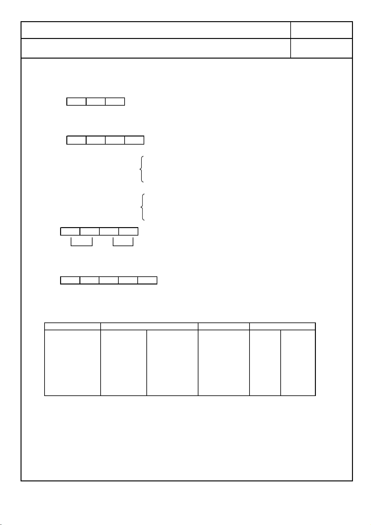
1. Scope
Fixed capacitors for use in electronic equipment, Aluminum electrolytic capacitors with non-solid electrolyte.
2. Parts Number
2-1 2-2 2-3 2-4 2-5 2-4 2-6
2-1 Aluminum Electrolytic Capacitor
2-2 Type : Radial lead type ( JIS : 04 type )
2-3 Rated Voltage Code
2-4 AK series X type
2-5 Capacitance Code : Indicating capacitance in uF by 3 letters.
The first 2 figures are actual values and the third
denotes the number of zeros.
"R" denotes the decimal point and all figures are the
actual number with "R".
For example, 1uF is expressed as 1R0 in this case.
ex. 0. 1µF → 0R1 , 10µF → 100 , 1000µF → 102
2-6 Suffix Code for Appearance : Special Code for Appearance
Item 9 for snap-in lead,
Item 10 for lead taping dimensions,
Item 11 and Item 12 for lead taping specifications.
EC A ○○ AK ○○○ X □
Voltage Code 0J 1A 1C 1E 1V 1H
Rated Voktage (V.DC) 6.3 10 16 25 35 50
Blank Standard Long Lead
E Snap-in lead
i Lead taping (2.5mm pitch)
B Lead taping (5.0mm pitch)
Q Lead taping (5.0mm pitch:For φ8×7 only)
2
Panasonic Electronic Devices Co.,Ltd.
Page 5
Engineering Draft
CE-AAKX-CEM-1
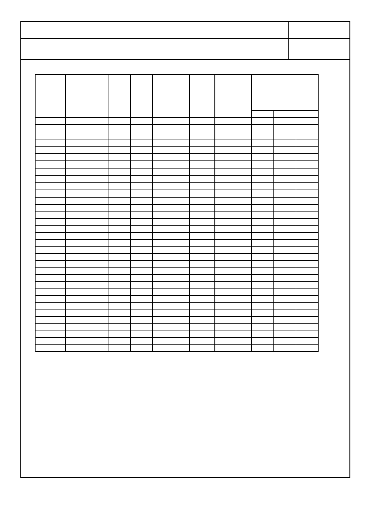
Parts Lists
A type AK series X type
Tangent
Part No. W.V. Cap. of loss
[V.DC] [µF] angle [µA] [mA rms]
max. max. max.
(120Hz) (120Hz) (After (120Hz)
(20℃)(20℃) 2 min.) (85℃) φDLφd
ECA0JAK470X 6.3 47 0.33 3.0 46 4 7 0.45
ECA0JAK101X 6.3 100 0.33 6.3 71 5 7 0.45
ECA0JAK221X 6.3 220 0.33 13.8 103 6.3 7 0.45
ECA0JAK331X 6.3 330 0.33 20.7 130 8 7 0.45
ECA1AAK330X 10 33 0.25 3.3 43 4 7 0.45
ECA1AAK221X 10 220 0.25 22 120 8 7 0.45
ECA1CAK220X 16 22 0.20 3.5 39 4 7 0.45
ECA1CAK330X 16 33 0.20 5.2 60 5 7 0.45
ECA1CAK470X 16 47 0.20 7.5 70 5 7 0.45
ECA1CAK101X 16 100 0.20 16.0 91 6.3 7 0.45
ECA1EAK100X 25 10 0.15 3.0 28 4 7 0.45
ECA1EAK220X 25 22 0.15 5.5 55 5 7 0.45
ECA1EAK470X 25 47 0.15 11.7 70 6.3 7 0.45
Leakage
Current
Rated Ripple
Current
Dim.[mm
]
3
ECA1VAK330X 35 33 0.12 11.5 65 6.3 7 0.45
ECA1VAK470X 35 47 0.12 16.4 85 8 7 0.45
ECA1HAK0R1X 50 0.1 0.10 3.0 1 4 7 0.45
ECA1HAKR22X 50 0.22 0.10 3.0 2 4 7 0.45
ECA1HAKR33X 50 0.33 0.10 3.0 3 4 7 0.45
ECA1HAKR47X 50 0.47 0.10 3.0 5 4 7 0.45
ECA1HAKR68X 50 0.68 0.10 3.0 7 4 7 0.45
ECA1HAK010X 50 1 0.10 3.0 10 4 7 0.45
ECA1HAK2R2X 50 2.2 0.10 3.0 16 4 7 0.45
ECA1HAK3R3X 50 3.3 0.10 3.0 16 4 7 0.45
ECA1HAK4R7X 50 4.7 0.10 3.0 23 4 7 0.45
ECA1HAK100X 50 10 0.10 5.0 35 5 7 0.45
ECA1HAK220X 50 22 0.10 11.0 60 6.3 7 0.45
ECA1HAK330X 50 33 0.10 16.5 75 8 7 0.45
Panasonic Electronic Devices Co.,Ltd.
Page 6
Engineering Draft
CE-AAKX-CEM-1
A type AK series X type
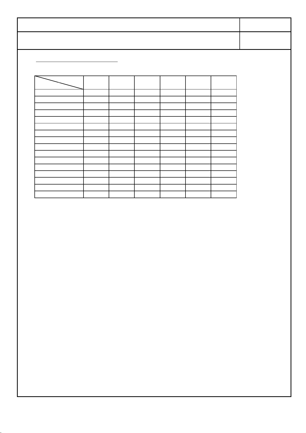
4
Capacitance and Can Size Table
φDxL[mm]
4x7
4x7
4x7
4x7
4x7
4x7
4x7
4x7
4x7
4x7
Can Size(φD×L
0.1
0.22
0.33
0.47
0.68
1
2.2
3.3
4.7
10
22
33
47
100
220
330
V.DC
)
4x7 4x7 5x7 6.3x7
4x7
5x7
→
→
5x7
5x7 6.3x7 8x7
6.3x7 8x7 6.3x7
8x7
256.3 10 16
35 50
4x7 5x7
→
6.3x7 8x7
Please refer to a high-ranking voltage for "→".
Panasonic Electronic Devices Co.,Ltd.
Page 7
Engineering Draft
CE-AAKX-CEM-1
A type AK series X type
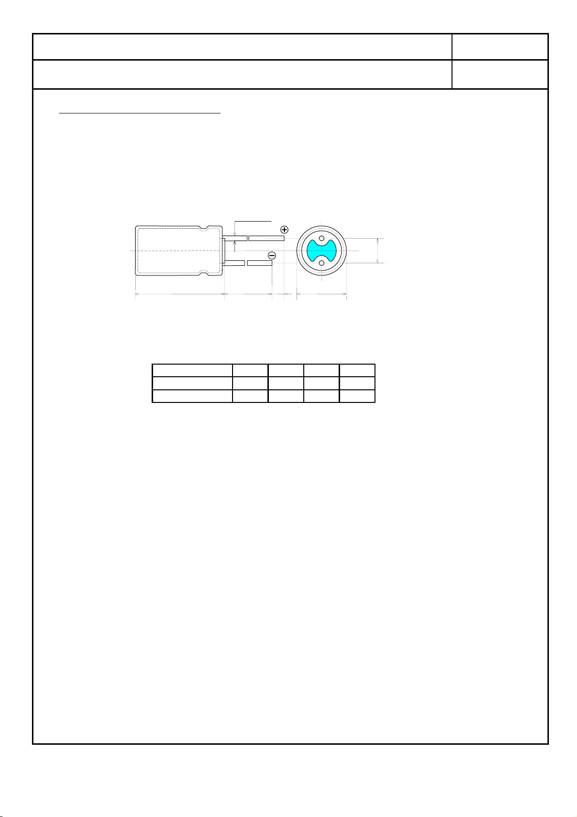
3. Dimensions and Appearance
Body Color ( Clear Blue) , Marking ( White )
Standard Long Lead (Suffix : Blank)
φd±0.05
L±1.0
14min
3
min.
φD±0.5
Body Dia. φD456.38
Lead Space F 1.5 2.0 2.5 2.5
Lead Dia. φd 0.450.450.450.45
Please refer to L dimension on the parts number lists table.
[mm]
F±0.5
[mm]
5
Panasonic Electronic Devices Co.,Ltd.
Page 8
Engineering Draft
A
CE-AAKX-CEM-1
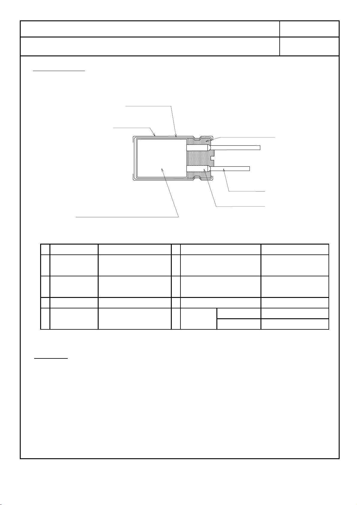
4. Constructions
4-1 Inside Construction
4-2 Construction Parts
Inside uni
(5 Separator、6・7Anode and、
Cathode foil、8 Electrolyte)
Parts Materials Materials
A type AK series X type
3 Aluminum can
2 Sleeve
t
6
4 Sealing rubber
1 Lead wire
luminum Lead
Parts
1 Lead Wire Solid tinned copper weld 5 Separator Manila hemp
steel wire
2 Sleeve Thermoplastic Resin 6 Anode Foil High purity
3 Aluminum Can Aluminum 7 Cathode Foil Aluminum foil
4 Sealing Rubber Synthetic rubber 8 Electrolyte Main Solvent
(EPT/IIR) Main Solute
5. Marking
Markings indicated on the products :
a ) Rated Voltage.
b ) Capacitance
c ) Negative Polarity
d ) Manufacturer’s Trademark
e ) Upper Category Temperature
f ) Lot No. (It indicates to Lot No. System)
Aluminum foil
Ethlene glycol
Ammonium salt
Panasonic Electronic Devices Co.,Ltd.
Page 9
Engineering Draft
A
A
CE-AAKX-CEM-1
Radial lead type Lot No. System 7
・JAPAN PRODUCTS
Lot number is indicated on a sleeve in following manner.
eg. For 04 type, expressed in 3 figures, 4 figures, or 5 figures.
(a) (b) (c)
(a)sequential alphabet for each lot
(b)month (1 to 9 and O for October, N for November, D for December)
(c)sequential alphabet for
(a) (b) (c) (d)
As for the display contents of 4 figures, there are 2 kinds
(1) (a) last number of year
(b) month (1 to 9 and O for October, N for November, D for December)
(c) week (1 to 5 and A to E)
(d) line code in alphabet (A to Z)
(2) (a) last number of year
(b) month (1 to 9 and O for October, N for November, D for December)
(c) line code in alphabet (A to Z)
(d) production date
(a) (b)
(a) last 2 digit of year
(b) numerical indication of week (ninth week of 1992=09)
(a) (b) (c) (d) -
(a) last number of year
(b) month (1 to 9 and O for October, N for November, D for December)
(c) week (1 to 5 and A to E)
(d) line code
production year production week
1:2001 1:January 7:July
2:2002 2:February 8:August B,2:second week B=2 2=28
3:2003 3:March 9:September C,3: third week C=3 3=29
4:2004 4:April O:October D,4: forth week
~
Indicating with the 6:June D:December Z=26
last digit or the
last 2 digits of a
year.
* Lot number can be written in both horizontal and vertical directions.
* Manufacturing country for certain products may not be indicated.
and shifts operation.
※ Letters and marks are also used to distinguish different lines, machines
production month production date
,1: first week
5:May N:November E,5: fifth week Y=25 5=31
=1 date 1=27 date
~
4=30
Panasonic Electronic Devices Co.,Ltd.
Page 10

Engineering Draft
r
A
r
r
r
A
Radial lead type Lot No. System 8
・MALAYSIA PRODUCTS
Lot number is indicated on a sleeve in following manner.
eg. For 04 type, expressed in 4 figures, or 5 figures.
(a) (b) (c) (c)
(a) last number of year
(b) month (1 to 9 and O for October, N for November, D for December)
(c) line code in alphabet (A to Z)
(a) (b) (b) (a)
(a) last number of year and line code in alphabet (A to Z)
(b) month (1 to 9 and O for October, N for November, D for December)
and production date
(a) (b) (c) (d) (d)
(a) last number of year
(b) month (1 to 9 and O for October, N for November, D for December)
(c) week (Greece number)
(d) line code
(a) (b) (c)
(d) (d)
(a) last number of year
(b) month (1 to 9 and O for October, N for November, D for December)
(c) week (Greece number)
(d) line code
production yea
1:2001 1:January 7:July
2:2002 2:February 8:August
3:2003 3:March 9:Septembe
4:2004 4:April O:Octobe
~ 5:May N:Novembe
Indicating with the 6:June D:December
Ⅰ: first week
Ⅱ:second week
Ⅲ: third week
: forth week
Ⅳ
Ⅴ: fifth week
,1: first week 1:1date B:11date
B,2:second week 2:2date C:12date
C,3: third week 3:3date
D,4: forth week
E,5: fifth week 9:9date V:31date
CE-AAKX-CEM-1
production date production month production week
~
U:30date
:10date
~
last digit or the
last 2 digits of a
year.
Panasonic Electronic Devices Co.,Ltd.
Page 11

Engineering Draft
CE-AAKX-CEM-1
6. Standard Ratings
No.
1 Category Temperature Range -40℃ ~ +85
2 Rated Voltage Range 6.3 V.DC ~ 50 V.DC
3 Capacitance Range 0.1 µF ~ 330 µF (120Hz 20℃)
4 Capacitance Tolerance ± 20% (120Hz 20℃)
5 Surge Voltage R.V. 6.3 10 16 25 35 50
(V.DC) S.V. 8 1320324463
6 Rated Ripple Current Parts Lists and Table3
A type AK series X type
Item Ratings
9
℃
Panasonic Electronic Devices Co.,Ltd.
Page 12

Engineering Draft
CE-AAKX-CEM-1
A type AK series X type
7. Performance Characteristics
No Item Performance Characteristics Test
1 Leakage Current ≦ I = 0. 01CV or 3µA, whichever is
greater.
I : Leakage current C : Capacitance
V : Rated voltage
2 Capacitance Within the specified capacitance
tolerance.
3 Tangent of Loss Less than the table 1 value of item 8.
Angle
(tanδ)
4 Characteristics at Step 2
High and Low Impedance Ratio :
Temperature Ratio for the value in step 1 shall
be less than the value from table 2
in item 8. *
Step 4
Leakage Current :
500% of the value of item 7. 1. *
≦
Capacitance Change : Impedance should be measured at the frequency
Within ±25% of the value in step 1 of 120 Hz±10%.
Tangent of Loss Angle (tanδ):
the value of item 7. 3.
≦
5 Surge Leakage Current : Test Temperature : 15℃ ~ 35
the value of item 7.1.
≦
Capacitance Change : Series Protectiv e Resistance :
Within ±15% of the initially
measured value.
Tangent of Loss Angle (tanδ): R = Series protective resistance (kΩ)
the value of item 7. 3. C =Capacitance (µF)
≦
Appearance : Test Voltage : Surge voltage item 6. 5
No significant change can be Applied Voltage : 1000 cycles of 30s±5s
observed.
Series Resistor : 1000Ω±10Ω
Applied Voltage : Rated voltage
Measuring : After 2 minutes
Measuring Frequency
Measuring Circuit
Measuring Voltage
Measuring Frequency
Measuring Circuit
Measuring Voltage
Test Temperature (℃)Step
1
3
4
5
* Capacitors should be stored at each
temperature until measured impedance or
capacitance is stabilized.
: 120 Hz±20%
: Equiv alent series circuit
: +1. 5V. DC ~ +2 V. DC
( ≦0.5V for AC.)
: 120 Hz±20%
: Equiv alent series circuit
: +1. 5V. DC ~ +2 V. DC
( ≦0.5V for AC.)
20± 2
-40±32
20±
2
85± 2
20± 2
℃
100 ± 50
R =
C
“ON” and 5 min. 30 s "OFF"
10
Time
15 minutes
2 hours
Panasonic Electronic Devices Co.,Ltd.
Page 13

Engineering Draft
g
y
g
g
CE-AAKX-CEM-1
A type AK series X type
No Item Performance Characteristics Test
6 Robustness of
Terminations Diameter [mm] Pull Strength
Tensile φ0.45 5 N
There is no damage or breakage after Applied above steady pull axially for a 10s±1s
Bending test.
Diameter [mm ] Static Load
φ0.45 2.5 N
At first, a capacitor is placed in vertical position
with the weight specified above being applied to
one of leads. Then the capacitor is slowly
rotated 90°to horizontal position and
subsequently returned to vertical position.
The above bendin
An additional bending is done in the opposite
direction.
7 Vibration Capacitance : Frequency
Measured value is to be stabilized (1 minute per cycle.)
during test. (Measured several Total Amplitude : 1. 5 mm
times within 30 min. Direction and Duration of Vibration :
before completion of test) It is done in the X, Y, Z axis direction for 2
Appearance : hours each, with a total of 6 hours.
No significant change can be Mounting Method :
observed. The capacitor shall be fixed with its lead wires
Capacitance Change : at the point of 4 mm from the bottom of
W ithin ±5% of the initiall
measured value.
capacitor body.
11
procedure takes for 2s ~3s
: 10 Hz ~55 Hz
8 Solderability M ore than 3/4 of the term inal surface Solder Type : H60A, H60S, or H63A (JIS Z3282)
shall be covered with new solder. Solder Temperature
Immersing Time : 2s±0. 5s
Immersing Depth
Flux : Approx. 25% rosin (JIS K5902)
9 Resistance to Leakage Current : Solder Type : H60A, H60S, or H63A (JIS Z3282)
Soldering Heat
≦ the value of item 7.1.
Capacitance Chan
W ithin ±10% of the initially Im m ersing Depth
measured value.
Tangent of Loss Angle (tanδ):
≦
the value of item 7. 3.
Appearance :
nificant change can be
No si
observed.
e : Immersing Time : 10s±1s
Solder Temperature
: 235℃±5
: 1. 5mm ~ 2. 0mm from the root.
in ETHANOL (JIS K8101)
: 260℃±5℃
: 1. 5mm ~ 2. 0mm from the root.
℃
Panasonic Electronic Devices Co.,Ltd.
Page 14

Engineering Draft
p
CE-AAKX-CEM-1
A type AK series X type
No Item Performance Characteristics Test
10
Solvent There shall be no damage and legible Class of Reagent : Isopropyl Alcohol
Resistance of marking. Marking can be easily Test Temperature : 20℃ ~ 25℃
Marking comprehended. Immersing Time : 30s±5s
11 Damp Heat Leakage Current : Test Temperature : 40℃±2℃
(Steady state)
12 Endurance Leakage Current : Test Temperature : 85℃±2
13 Shelf Life Leakage Current : Test Temperature : 85℃±2℃
* Voltage treatment :
resistors (1000Ω±10Ω), for 30 minutes as a posttest treatment (performing discharge).
the value of item 7.1. Relative Humidity : 90% ~ 95%
≦
Capacitance Change : Test Duration : 240hours ±8hours
Within ±20% of the initially
measured value. After subjected to the test, capacitors shall
Tangent of Loss Angle (tanδ): be left for 2 hours at room temperature and
≦ 120% the value of item 7. 3. room humidity prior to the measurement.
Appearance :
No significant change can be
observed.
℃
the value of item 7.1. Test Duration
≦
Capacitance Change : Applied Voltage : Rated Voltage .
Within ±20% of the initially
measured value. After subjected to the test, capacitors shall be left at
Tangent of Loss Angle (tanδ): room temperature and room humidity for 2 hours prior
200% of the value of item 7. 3. to the measurement.
≦
Appearance :
No significant change can be
observed.
the value of item 7.1. Test Duration
≦
Capacitance Change :
Within ±20% of the initially
measured value. After subjected to the test with no voltage applied,
Tangent of Loss Angle (tanδ):
≦ 200% of the value of item 7. 3. be left for 2 hours at room temperature and
Appearance : humidity prior to the measurement.
No significant change can be
observed.
acitors shall undergo voltage treatment*and
ca
: 1000
: 500
+48
hours
0
+48
The rated voltage shall be applied to the capacitors, which are connected to series protective
hours
0
12
Panasonic Electronic Devices Co.,Ltd.
Page 15

Engineering Draft
CE-AAKX-CEM-1
A type AK series X type
8. Other Characteristics
■ Table 1. Tangent of Loss Angle(tanδ)
V.DC 6.31016253550
D.F. 0.33 0.25 0.20 0.15 0.12 0.10
■ Table 2.Characteristics at low temperature Impedance ratio (at 120 Hz)
V.DC 6.31016253550
Z(-40℃)/Z(20℃)864433
■ Table 3.Frequency Correction Factor of Rated Ripple Current
50,60 120 1k 10k
Coefficient 0.7 1 1.3 1.7
13
Frequency (Hz)
~
Panasonic Electronic Devices Co.,Ltd.
Page 16

Engineering Draft
φ
CE-AAKX-CEM-1
A type AK series X type
14
9. Snap-In Lead Formed Type ( Part No. Suffix : E )
φ4~φ8
[mm]
H2
F
P
E
φD±0.5
[mm]
φ t
d
H3
H1
* Direction of bending is random.
φD H1±0.5 H2 H3±0.3 F±0.5 P E max. φd±0.05 P.W .B
4 4.5 2.7 1.5 5.0 0.95 1.0 0.45 0.9 1.6
5 4.5 2.7 1.5 5.0 0.95 1.0 0.45 0.9 1.6
6.3 4.5 2.7 1.5 5.0 0.95 1.0 0.45 0.9 1.6
8 4.5 2.7 1.5 5.0 0.95 1.0 0.45 0.9 1.6
*The lead forming dimensions above shall only be subjected to our outgoing inspection and
not to the customer's incoming inspection.
Due to the application of mechanical stress during transportation, actual dimensions might
not meet the specification.
Panasonic Electronic Devices Co.,Ltd.
Page 17

Engineering Draft
∆
CE-AAKX-CEM-1
A type AK series X type
15
10.Lead Taping
10-1. Lead Taping ( Body Diameter φ4 ~φ6. 3 ) The Suffix of Taping Part Number : i
1) Applicable Range
This specification is applied to products, which are Aluminum Electrolytic Capacitors (JIS04 type)
that taped with single tape.
2) Taping Shape & Dimensions
φ4 ,φ.5 φ6.3
∆P
P2
P
φD
h
∆P
P2
φD
P
∆h
L
L
W2
W0
w
F
P1
W1
H
W
W2
W0
P1
F
H
W1
P0
φd
φD0
t
P0
φd
φD0
t
[mm]
Item Symbol Dimensions Tolerance Remarks
Body diameter
Body length
Lead wire diameter
Body pitch
Feed hole pitch *1
Hole center to lead
Feed hole center
to product center
Lead to lead distance
Mount tape
Adhesive tape
Hole position
Adhesive tape slipping
Height of product
from the center
Feed hole diameter
Inclination of body
Inclination of body
Total tape thickness
φD456.3±0.5
L ---
7.0
φd 0.45 ±0.05
P 12.7 ±1.0
P0 12.7 ±0.2
P1
5.1
±0.5
P2 6.35 ±1.00
F
2.5
±0.5
W 18.0 ±0.5
W0 6.0
≦
W1 9.0 ±0.5
W2 0 ~1.5 ---
H 18.50
+0.75
-0.50
φD0 4.0 ±0.2
h1.0 ≧---
△
P1.0 ≧---
△
t0.6±0.3
Specified by the contact surface between
tape & lead
ditto
---
Specified at the top of the body
ditto
CP wire is excluded
*1 Cumulative deviation of “feed hole pitch” shall be less than 1 mm in 20 sections.
Panasonic Electronic Devices Co.,Ltd.
Page 18

Engineering Draft
CE-AAKX-CEM-1
A type AK series X type
16
10-2. Lead Taping ( Body Diameter φ8 ) The Suffix of Taping Part Number : i
1) Applicable Range
This specification is applied to products, which are Aluminum Electrolytic Capacitors (JIS04 type)
that taped with single tape.
2) Taping Shape & Dimensions
∆P
P2
W
W2
W0
P1
F
P0
Item Symbol Dimensions Tolerance Remarks
Body diameter
Body length
Lead wire diameter
Body pitch
Feed hole pitch *1
Hole center to lead
Feed hole center
to product center
Lead to lead distance
Mount tape
Adhesive tape
Hole position
Adhesive tape slipping
Height of product
from the center
Feed hole diameter
Inclination of body △
Inclination of body
Total tape thickness
φD8±0.5
L 7.0 ---
φd 0.45 ±0.05
P 12.7 ±1.0
P0 12.7 ±0.2
P1
P2 6.35
F
W 18.0 ±0.5
W0 6.0
W1 9.0 ±0.5
W2 0 ~1.5 ---
H18.50
φD0 4.0 ±0.2
h1.0 ≧--P1.0 ≧---
△
t 0.6 ±0.3
*1 Cumulative deviation of “feed hole pitch” shall be less than 1 mm in 20 sections.
P
5.1
2.5
≦
φD
φd
∆h
L
H
W1
φD0
±0.5
±1.00
±0.5
Specified by the contact surface between
tape & lead
ditto
t
---
+0.75
-0.50
Specified at the top of the body
ditto
CP wire is excluded
[mm]
Panasonic Electronic Devices Co.,Ltd.
Page 19

Engineering Draft
CE-AAKX-CEM-1
A type AK series X type
17
10-3 Lead Taping ( Body Diameter φ4 ~φ6. 3 ) The Suffix of Taping Part Number : B
1) Applicable Range
This specification is applied to products, which are Aluminum Electrolytic Capacitors (JIS04 type)
that taped with single tape.
2) Taping Shape & Dimensions
∆P
P2 P
φD
∆h
L
W2
W0
W
F
P1
H0
H
W1
P0
φd φD0
t
[mm]
Item Symbol Dimensions Tolerance Remarks
Body diameter
Body length
Lead wire diameter
Body pitch
Feed hole pitch *1
Hole center to lead
Feed hole center
to product center
Lead to lead distance
Mount tape
Adhesive tape
Hole position
Adhesive tape slipping
Height of product
from the center
Lead wire clinch height
Feed hole diameter
Inclination of body △
Inclination of body
Total tape thickness
φD 4 5 6.3 ±0.5
φd0.45±0.05
P0 12.7 ±0.2
P1
P2 6.35 ±1.00
W0 6.0
W1 9.0 ±0.5
W2 0 ~1.5 ---
H0 16.0
φD0 4.0 ±0.2
△
L7.0---
P 12.7 ±1.0
3.85
F
5.0
±0.5
+0.8
W 18.0 ±0.5
≦
H 17.50
+0.75
-0.20
±0.5
h1.0 ≧--P1.0 ≧---
t 0.6 ±0.3
Specified by the contact surface between
tape & lead
ditto
-0.2
---
Specified at the top of the body
ditto
CP wire is excluded
*1 Cumulative deviation of “feed hole pitch” shall be less than 1 mm in 20 sections.
*2 Lead forming angle
A=90°min
A
Panasonic Electronic Devices Co.,Ltd.
Page 20

Engineering Draft
CE-AAKX-CEM-1
A type AK series X type
10-4. Lead Taping ( Body Diameter φ8 ) The Suffix of Taping Part Number : Q
1) Applicable Range
This specification is applied to products, which are Aluminum Electrolytic Capacitors (JIS04 type)
that taped with single tape.
2) Taping Shape & Dimensions
∆P
P2
W
W2
W0
P1
F
P0
Item Symbol Dimensions Tolerance Remarks
Body diameter
Body length
Lead wire diameter
Body pitch
Feed hole pitch *1
Hole center to lead
Feed hole center
to product center
Lead to lead distance
Mount tape
Adhesive tape
Hole position
Adhesive tape slipping
Height of product
from the center
Lead wire clinch height
Feed hole diameter
Inclination of body △
Inclination of body
Total tape thickness
φD8±0.5
L 7.0 ---
φd 0.45 ±0.05
P 12.7 ±1.0
P0 12.7 ±0.2
P1
P2
3.85
F
W 18.0 ±0.5
W0 6.0
W1 9.0 ±0.5
W2 0 ~1.5 ---
H
18.5
H0 16.0
φD0 4.0 ±0.2
h1.0 ≧--P1.0 ≧---
△
t 0.6 ±0.3
*1 Cumulative deviation of “feed hole pitch” shall be less than 1 mm in 20 sections.
*2 Lead forming angle
A=90°min
P
5.0
≦
φD
6.35
φd
∆h
L
H
W1
φD0
±1.00
±0.5
+0.8
Specified by the contact surface between
tape & lead
ditto
t
-0.2
---
+0.75
-0.50
±0.5
Specified at the top of the body
ditto
CP wire is excluded
18
[mm]
A
Panasonic Electronic Devices Co.,Ltd.
Page 21

Engineering Draft
CE-AAKX-CEM-1
A type AK series X type
19
11. Taping Method
11-1 The capacitors shall be placed vertically on the base tape, and their lead wires are fixed with
the adhesive tape. In addition, the direction of polarity is standardized as the base tape
is situated underneath of an adhesive tape, and lead wires with the same polarity are placed on
the right hand side (the direction of polarity for bipolar products is not specified).
(Examples)
*Polarity direction
φ4 ~ φ8: Negative polarity on the right.
11-2 After taping, there shall be no more than three blank spaces without lead wires on the base tape.
The number of blank spaces within a packing unit (an inner carton) is not restricted, however,
the specified packing quantity must be satisfied.
11 - 3 The connection method is as follows. The portion shall meet the general taping specification.
The position of connection shall not be restricted.
Base tapes shall not be connected with each other by using staples.
Adhesive tape
Note ) When connecting two base tapes, they shall not be piled on top of each other.
Connecting point
Base
Connect with the
adhesive tape
Panasonic Electronic Devices Co.,Ltd.
Page 22

Engineering Draft
CE-AAKX-CEM-1
A type AK series X type
11-4 In case of removing the products after taping, lead wires shall be cut or the capacitor
shall be pulled out.
The length of remaining lead wire shall be less than 2.0 mm from the upper edge of
the base tape.
2mm max.
11-5 Tensile strength of lead wire after taping (specified for the positive lead wire only) :
Fix the tape as below and pull the positive lead wire to the vertical direction by using the
push pull scale.
The tensile strength shall be greater than 2. 94 N.
After continuously storing in an atmosphere of 40℃±2℃ and 90% ~ 98% for 250 hours,
the taped products shall meet the specification above, and there shall be no inclination
of the capacitors or covering of holes with the adhesive.
Lead wire
Base
Push pull scale
Lead wire
Fixed
Adhesive tape
20
Panasonic Electronic Devices Co.,Ltd.
Page 23

Engineering Draft
(a)
CE-AAKX-CEM-1
A type AK series X type
21
12. Packing Method
12-1 Taped products shall be packed in an inner carton ( the smallest packing unit ) in the zigzag pattern.
In an inner carton, the lead wires with positive polarity are not to be placed on the top of lead wires
with negative polarity and vice versa (however, the last sentence does not apply to bipolar products).
(Examples)
Inner packing
case
φ4~φ8
φ10
~
φ18
12-2 Polarity identifications on an inner carton shall match the polarity of products situated inside
the inner carton.
12-3 Inner cartons shall be handled as follows.
* No more than 10 inner cartons shall be piled on top of each other.
* In case of situating cartons in upright position, the indication of polarity shall be faced upward.
* The products shall be handled with care.
<Right> <Wrong>
○ ○
×
12-4 The inner cartons shall be packed in a cardboard box for transportation.
Products with various part numbers can be packed in an outer carton upon request.
However, each inner carton (the smallest packing unit) shall only contain products
with the same part number.
12-5 The shape & dimensions of inner cartons shall be as follows.
(b)
Can size
φDL
φ4 ~φ8 7 340 55 320
Note : The dimensions listed above are subject to
(c)
change without notice, depending on the
auto-insert machine.
No unit at
The corner.
×
(a) (b) (c)
[mm]
Panasonic Electronic Devices Co.,Ltd.
Page 24

Engineering Draft
(5) φ
CE-AAKX-CEM-1
Radial lead type Package Amount and Shape
Label information on the packing box. Package Label Example
The label has following information in English Long lead , Lead formed Outer Box
a ) Rated Voltage, Capacitance
b ) Manufacturer’s Trademark
c ) Part Number
d ) Packing Quantity
e ) Serial No.
f ) Manufacturer’s Name
g ) Country of Origin
Long lead , Lead formed (Unit:pcs)
Long lead Lead formed
Can size
φ4x7 200 10000 200 10000
φ5x7 200 10000 200 10000
φ6.3x7 200 10000 200 10000
φ8x7 200 4000 200 4000
Package Material
Inner Vinyl bag
Outer Card board
Packaging Packaging Packaging Packaging
Quantity Quantity per box Quantity Quantity per box
Long lead
Lead formed
Contents of label description
(1) Customer Part No.
(2) Quantity
(3) Rated Capacitance
(4) Voltage
(5) Can Size
(6) Product Part No.
<JAPAN PRODUCTS>
Customer Part No.
(1)
(3N)1 (1) (2)
(3N)2 Y5201R41A001 108010
FIXED ALUMINIUM ELECTROLYTIC CAPACITOR
(6)
(2)
Serial No. Y5201R41A001
Panasonic Electronic Devices Co.,Ltd.
M
(3) uF (4) V
MADE IN JAPAN EIAJ C-3 001
G
22
× L
<MALAYSIA PRODUCTS>
Customer Part No.
(1)
(3N)1 (1) (2)
(3N)2 D0002R03D428 108010
FIXED ALUMINIUM ELECTROLYTIC CAPACITOR
(6)
Panasonic Electronic Devices (M) Sdn. Bhd.
M
EIAJ-C3 PEDMA(SA) Made in Malaysia
Production month
Panasonic Electronic Devices Co.,Ltd.
(5) φ X L
Serial No.
D0002R03D428
G
(3) uF
(4) V
(2)
PCS
.
Page 25

Engineering Draft
(5) φ
CE-AAKX-CEM-1
Radial lead type Package Amount and Shape
Label information on the packing box.
The label has following information in English
a ) Rated Voltage, Capacitance
b ) Manufacturer’s Trademark
c ) Part Number
d ) Packing Quantity
e ) Serial No.
f ) Manufacturer’s Name
g ) Country of Origin
Taping (Unit:pcs)
Box
Can size
φ4 2000 10000
φ5 2000 10000
φ6.3 2000 10000
φ8 1000 5000
Packaging Packaging
Quantity Quantity per box
Package Label Example Taping Outer Box
Contents of label description
(1) Customer Part No.
(2) Quantity
or
(3) Rated Capacitance
(4) Voltage
(5) Can Size
(6) Product Part No.
<JAPAN PRODUCTS> <MALAYSIA PRODUCTS>
Customer Part No.
(1)
(3N)1 (1) (2)
(3N)2 Y5201R41A001 108010
FIXED ALUMINIUM ELECTROLYTIC CAPACITOR
(6)
(2)
Serial No. Y5201R41A001
Panasonic Electronic Devices Co.,Ltd.
MADE IN JAPAN EIAJ C-3 001
M
G
(3) uF (4) V
× L
Customer Part No.
(1)
(3N)1 (1) (2)
(3N)2 D0002R03D428 108010
FIXED ALUMINIUM ELECTROLYTIC CAPACITOR
(6)
Panasonic Electronic Devices (M) Sdn. Bhd.
M
EIAJ-C3 PEDMA(SA) Made in Malaysia
Production month
(5) φ X L
Serial No.
D0002R03D428
Package Material
Taping
Inner Card board
Outer Card board
23
G
(3) uF
(4) V
(2)
PCS
.
Panasonic Electronic Devices Co.,Ltd.
Page 26

Engineering Draft
(5) φ
CE-AAKX-CEM-1
Radial lead type Package Amount and Shape
24
Taping Inner Box
Contents of label description
(1) Customer Part No.
(2) Quantity
(3) Rated Capacitance
(4) Voltage
(5) Can Size
(6) Product Part No.
<JAPAN PRODUCTS> <MALAYSIA PRODUCTS>
Customer Part No.
(1)
(3N)1 (1) (2)
(3N)2 Y5201R41A001 108010
FIXED ALUMINIUM ELECTROLYTIC CAPACITORS
Panasonic Electronic Devices Co.,Ltd. EIAJ C-3 MADE IN JAPAN 001
M
G
(6)
(3) uF (4) V
× L
Serial No. Y5201R41A001
(2) PCS.
Customer Part No.
(1)
(3N)1 (1) (2)
(3N)2 D0002R03D428 108010
FIXED ALUMINIUM ELECTROLYTIC CAPACITOR
(6)
Panasonic Electronic Devices (M) Sdn. Bhd.
M
EIAJ-C3 PEDMA(SA) Made in Malaysia
Production month
(5) φ X L
Serial No.
D0002R03D428
Storage
1. With respect to the handling method, follow Item 12-3 in this specification.
2. Products shall be out of direct sun light. In addition, the temperature and humidity shall be normal.
Minimum order quantity
The order shall be placed with a multiple of the inner carton quantity.
Examples : φ4 ~ φ6. 3 : minimum 2000 pcs
φ8 : minimum 1000 pcs
G
(3) uF
(4) V
(2)
PCS
.
Panasonic Electronic Devices Co.,Ltd.
Page 27

Engineering Draft
CE-AAKX-CEM-1
Application Guidelines
* This specification guarantees the quality and performance of the product as individual components.
Before use, check and evaluate their compatibility with installed in your products.
* Do not use the products beyond the specifications described in this document.
* Install the following systems for a failsafe design to ensure safety if these products are to be used in equipment where a defect in these
products may cause the loss of human life or other signification damage, such as damage to vehicles (automobile, train, vessel), traffic
lights, medical equipment, aerospace equipment, electric heating appliances, combustion/ gas equipment, rotating equipment, and
disaster/crime prevention equipment.
・The system is equipped with a protection circuit and protection device.
・The system is equipped with a redundant circuit or other system to prevent an unsafe status in the event of a single fault.
* Before using the products, carefully check the effects on their quality and performance, and determined whether or not they can be used.
These products are designed and manufactured for general-purpose and standard use in general electronic equipment.
These products are not intended for use in the following special conditions.
1. In liquid, such as Water, Oil, Chemicals, or Organic solvent
2. In direct sunlight, outdoors, or in dust
3. In vapor, such as dew condensation water of resistive element, or water leakage, salty air, or air with a high concentration corrosive
1. Circuit Design
1.1 Operating Temperature and Frequency
Electrical parameters for electrolytic capacitors are normally specified at 20℃ temperature and 120 Hz frequency.
These parameters vary with changes in temperature and frequency. Circuit designers should take these changes into consideration.
(1) Effects of operating temperature on electrical parameters
(2) Effects of frequency on electrical parameters
b) At lower frequencies, heat generated by ripple current will rise due to an increase in equivalent series resistance (ESR).
1.2 Operating Temperature and Life Expectancy
Check for the maximum capacitor operating temperatures including ambient temperature, internal capacitor temperature rise due to
Avoid placing components, which could conduct heat to the capacitor from the back side of the circuit board.
(3) The formula for calculating expected life at lower operating temperatures is as follows ;
L
L
T
T
gas, such as Cl2, H2S, NH3, SO2, or NO2
4. In an environment where strong static electricity or electromagnetic waves exist
5. Mounting or placing heat-generating components or inflammables, such as vinyl-coated wires, near these products
6. Sealing or coating of these products or a printed circuit board on which these products are mounted, with resin and other material
7. Using resolvent, water or water-soluble cleaner for flux cleaning agent after soldering.
(In particular, when using water or a water-soluble cleaning agent, be careful not to leave water residues)
* Please arrange circuit design for preventing impulse or transitional voltage.
Do not apply voltage, which exceeds the full rated voltage when the capacitors receive impulse voltage, instantaneous high voltage,
high pulse voltage etc.
* Electrolyte is used in the products. Therefore, misuse can result in rapid deterioration of characteristics and functions of each product.
Electrolyte leakage damages printed circuit and affects performance, characteristics, and functions of customer system.
a) At higher temperatures, leakage current and capacitance increase while equivalent series resistance (ESR) decreases.
b) At lower temperatures, leakage current and capacitance decrease while equivalent series resistance (ESR) increases.
a) At higher frequencies, capacitance and impedance decrease while tanδ increases.
(1) Expected life is affected by operating temperature. Generally, each 10 ℃ reduction in temperature will double the expected life.
Use capacitors at the lowest possible temperature below the upper category temperature.
(2) If operating temperatures exceed the upper category limit, rapid deterioration of electrical parameter will occur and irreversible damage
will result.
ripple current, and the effects of radiated heat from power transistors, IC's or resistors.
T1-T
2
L2=L1x2
: Guaranteed life (h) at temperature, T1 ℃
1
: Expected life (h) at temperature, T2 ℃
2
: Upper category temperature (℃)
1
: Actual operating temperature, ambient temperature + temperature rise due to ripple current heating(℃)
2
10
25
(4) Please use according to the lifetime as noted in this specification. Using products beyond end of the lifetime may change characteristics rapidly,
short-circuit, operate pressure relief vent, or leak electrolyte.
Panasonic Electronic Devices Co.,Ltd.
Page 28

Engineering Draft
CE-AAKX-CEM-1
Application Guidelines
1.3 Common Application Conditions to Avoid
The following misapplication load conditions will cause rapid deterioration of a capacitor’s electrical parameters.
In addition, rapid heating and gas generation within the capacitor can occur, causing the pressure relief vent to operate and resultant leakage
of electrolyte. Under extreme conditions, explosion and fire ignition could result.
The leaked electrolyte is combustible and electrically conductive.
(1) Reverse Voltage
DC capacitors have polarity. Verify correct polarity before insertion. For circuits with changing or uncertain polarity, use DC bipolar
capacitors. DC bipolar capacitors are not suitable for use in AC circuits.
(2) Charge / Discharge Applications
Standard capacitors are not suitable for use in repeating charge/discharge applications. For charge/ discharge applications, consult us
with your actual application condition.
(3) Over voltage
Do not apply voltages exceeding the maximum specified rated voltage. Voltages up to the surge voltage rating are acceptable for
short periods of time.
Ensure that the sum of the DC voltage and the superimposed AC ripple voltage does not exceed the rated voltage.
(4) Ripple Current
Do not apply ripple currents exceeding the maximum specified value. For high ripple current applications, use a capacitor designed for
high ripple currents. In addition, consult us if the applied ripple current is to be higher than the maximum specified value.
Ensure that rated ripple currents that superimposed on low DC bias voltages do not cause reverse voltage conditions.
1.4 Using Two or More Capacitors in Series or Parallel
(1) Capacitors Connected in Parallel
The circuit resistance can closely approximate the series resistance of the capacitor, causing an imbalance of ripple current loads within
the capacitors. Careful wiring methods can minimize the possible application of an excessive ripple current to a capacitor.
(2) Capacitors Connected in Series
Differences in normal DC leakage current among capacitors can cause voltage imbalances.
The use of voltage divider shunt resistors with consideration to leakage currents can prevent capacitor voltage imbalances.
1.5 Capacitor Mounting Considerations
(1) Double-Sided Circuit Boards
Avoid wiring pattern runs, which pass between the mounted capacitor and the circuit board. When dipping into a solder bath,
an excess solder may deposit under the capacitor by capillary action, causing short circuit between anode and cathode terminals.
(2) Circuit Board Hole Positioning
The vinyl sleeve of the capacitor can be damaged if solder passes through a lead hole into the subsequently processed parts.
Special care when locating hole positions in proximity to capacitors is recommended.
(3) Circuit Board Hole Spacing
The spacing of circuit board holes should match the lead wire spacing of capacitors within the specified tolerances.
Incorrect spacing can cause an excessive lead wire stress during the insertion process.
This may result in premature capacitor failure due to the short or open circuit, increased leakage current, or electrolyte leakage.
(4) Clearance for Case Mounted Pressure Relief
Capacitors with case mounted pressure relief require sufficient clearance to allow proper pressure relief operation.
The minimum clearances are dependent of capacitor diameters as follows.
Dia. 6. 3 mm ~Dia. 16 mm : 2 mm minimum, Dia. 18 mm ~Dia. 35 mm : 3 mm minimum, Dia 40 mm or greater : 5 mm minimum.
(5) Clearance for Seal Mounted Pressure Relief
Provide a hole on a circuit board to relieve gas when a pressure relief of a capacitor is situated underneath of the circuit board.
(6) Wiring Near the Pressure Relief
Avoid locating high voltage, high current wiring, or circuit board paths above the pressure relief .
Flammable, high temperature gas that exceeds 100 ℃ may be released and could dissolve the wire insulation and ignite.
(7) Circuit Board Patterns Under the Capacitor
Avoid circuit board runs underneath the capacitor, as an electrical short can occur due to an electrolyte leakage.
(8) Screw Terminal Capacitor Mounting
Do not orient the capacitor with the screw terminal side of the capacitor facing downward.
Tighten the terminal and mounting bracket screws within the torque range specified in the specification.
1.6 Electrical Isolation of the Capacitor
Completely isolate the capacitor as follows.
(1) Between the cathode and the case (except for axially leaded B types) and between the anode terminal and other circuit paths.
(2) Between the extra mounting terminals (on T types) and the anode terminal, cathode terminal, and other circuit paths.
1.7 Capacitor Sleeve
The vinyl sleeve or laminate coating is intended for marking and identification purposes and is not meant to electrically insulate the capacitor.
26
The sleeve may split or crack if immersed into solvents such as toluene or xylene and then subsequently exposed to high temperatures.
Panasonic Electronic Devices Co.,Ltd.
Page 29

Engineering Draft
CE-AAKX-CEM-1
Application Guidelines
27
2. Capacitor Handling Techniques
2.1 Considerations Before Using
(1) Capacitors have a finite life. Do not reuse or recycle capacitors from used equipment.
(2) Transient recovery voltage may be generated in the capacitor due to dielectric absorption.
If required, this voltage can be discharged with a resistor with a value of about 1kΩ.
(3) Capacitors stored for a long period of time may exhibit an increase in leakage current.
This can be corrected by gradually applying rated voltage in series with a resistor of approximately 1kΩ.
(4) If capacitors are dropped, they can be damaged mechanically or electrically. Avoid using dropped capacitors.
(5) Dented or crushed capacitors should not be used. The seal integrity can be damaged and loss of electrolyte/shortened life can result.
2.2 Capacitor Insertion
(1) Verify the correct capacitance and rated voltage of the capacitor.
(2) Verify the correct polarity of the capacitor before insertion.
(3) Verify the correct hole spacing before insertion (land pattern size on chip type) to avoid stress on the terminals.
(4) Ensure that the lead clinching operation done by auto insertion equipments does not stress the capacitor leads where they enter the seal of
the capacitor.
For chip type capacitors, excessive mounting pressure can cause high leakage current, short circuit, or disconnection.
2.3 Manual Soldering
(1) Apply soldering conditions (temperature and time) based on the specification, or do not exceed temperature of 350 ℃ for 3
seconds or less.
(2) If lead wires must be modified to meet terminal board hole spacing, avoid stress on the lead wire where it enters the capacitor seal.
(3) If a soldered capacitor must be removed and reinserted, avoid excessive stress on the capacitor leads.
(4) Avoid physical contacts between the tip of the soldering iron and capacitors to prevent melting of the vinyl sleeve.
2.4 Flow Soldering
(1) Do not immerse the capacitor body into the solder bath as excessive internal pressure could result.
(2) Apply proper soldering conditions (temperature, time, etc.). Do not exceed the specified limits.
(3) Do not allow other parts or components to touch the capacitor during soldering.
2.5 Other Soldering Considerations
Rapid temperature rise during the preheat operation and resin bonding operation can cause cracking of the capacitor’s vinyl sleeve.
For heat curing, do not exceed 150 ℃ for the maximum time of 2 minutes.
2.6 Capacitor Handling after Soldering
(1) Avoid moving the capacitor after soldering to prevent excessive stress on the lead wires where they enter the seal.
(2) Do not use the capacitor as a handle when moving the circuit board assembly.
(3) Avoid striking the capacitor after assembly to prevent failure due to excessive shock.
2.7 Circuit Board Cleaning
(1) Circuit boards can be immersed or ultrasonically cleaned using suitable cleaning solvents for up to 5 minutes
and up to 60 ℃ maximum temperatures. The boards should be thoroughly rinsed and dried.
The use of ozone depleting cleaning agents is not recommended for the purpose of protecting our environment.
(2) Avoid using the following solvent groups unless specifically allowed in the specification ;
・ Halogenated cleaning solvents : except for solvent resistant capacitor types, halogenated solvents can permeate the seal and cause
internal capacitor corrosion and failure.
For solvent resistant capacitors, carefully follow the temperature and time requirements based on the
・ Alkaline solvents : could react and dissolve the aluminum case.
・ Petroleum based solvents : deterioration of the rubber seal could result.
・ Xylene : deterioration of the rubber seal could result.
・ Acetone : removal of the ink markings on the vinyl sleeve could result.
(3) A thorough drying after cleaning is required to remove residual cleaning solvents that may be trapped between the capacitor and the circuit
board. Avoid drying temperatures, which exceed the Upper category temperature of the capacitor.
(4) Monitor the contamination levels of the cleaning solvents during use in terms of electrical conductivity, pH, specific gravity, or water content.
Chlorine levels can rise with contamination and adversely affect the performance of the capacitor.
(5) Depending on the cleaning method, the marking on a capacitor may be erased or blurred.
Please consult us if you are not certain about acceptable cleaning solvents or cleaning methods.
2.8 Mounting Adhesives and Coating Agents
When using mounting adhesives or coating agents to control humidity, avoid using materials containing halogenated solvents.
Also, avoid the use of chloroprene based polymers.
Harden on dry adhesive or coating agents well lest the solvent should be left.
After applying adhesives or coatings, dry thoroughly to prevent residual solvents from being trapped between the capacitor and the circuit
board.
2.9 Fumigation
In exporting electronic appliances with aluminum electrolytic capacitors, in some cases fumigation treatment using such halogen
compound as methyl bromide is conducted for wooden boxes.
If such boxes are not dried well, the halogen left in the box is dispersed while transported and enters in the capacitors inside.
This possibly causes electrical corrosion of the capacitors. Therefore, after performing fumigation and drying make sure that no halogen
is left.
Don’t perform fumigation treatment to the whole electronic appliances packed in a box.
specification. 1-1-1 trichloroethane should never be used on any aluminum electrolytic capacitor.
Panasonic Electronic Devices Co.,Ltd.
Page 30

Engineering Draft
CE-AAKX-CEM-1
Application Guidelines
3. Precautions for using capacitors
3.1 Environmental Conditions
Capacitors should not be stored or used in the following environments.
(1) Exposure to temperatures above the upper category or below the lower category temperature of the capacitor.
(2) Direct contact with water, salt water, or oil.
(3) High humidity conditions where water could condense on the capacitor.
(4) Exposure to toxic gases such as hydrogen sulfide, sulfuric acid, nitric acid, chlorine, Chlorine compound, Bromine, Bromine compound or
ammonia.
(5) Exposure to ozone, radiation, or ultraviolet rays.
(6) Vibration and shock conditions exceeding specified requirements.
3.2 Electrical Precautions
(1) Avoid touching the terminals of a capacitor as a possible electric shock could result. The exposed aluminum case is not insulated and
could also cause electric shock if touched.
(2) Avoid short circuiting the area between the capacitor terminals with conductive materials including liquids such as acids or alkaline solutions.
4. Emergency Procedures
(1) If the pressure relief of the capacitor operates, immediately turn off the equipment and disconnect from the power source.
This will minimize an additional damage caused by the vaporizing electrolyte.
(2) Avoid contact with the escaping electrolyte gas, which can exceed 100 ℃ temperatures.
If electrolyte or gas enters the eye, immediately flush the eye with large amounts of water.
If electrolyte or gas is ingested by mouth, gargle with water.
If electrolyte contacts the skin, wash with soap and water.
5. Long Term Storage
Leakage current of a capacitor increases with long storage times. The aluminum oxide film deteriorates as a function of temperature and time.
If used without reconditioning, an abnormally high current will be required to restore the oxide film.
This surge current could cause the circuit or the capacitor to fail. After one year, a capacitor should be reconditioned by applying the rated
voltage in series with a 1000 Ω current limiting resistor for a time period of 30 minutes.
5.1 Environmental Conditions
(1) Exposure to temperatures above the upper category or below the lower category temperature of the capacitor.
(2) Direct contact with water, salt water, or oil.
(3) High humidity conditions where water could condense on the capacitor.
(4) Exposure to toxic gases such as hydrogen sulfide, sulfuric acid, nitric acid, chlorine, Chlorine compound, Bromine, Bromine compound or
ammonia.
(5) Exposure to ozone, radiation, or ultraviolet rays.
(6) Vibration and shock conditions exceeding specified requirements.
6. Capacitor Disposal
When disposing capacitors, use one of the following methods.
(1) Incinerate after crushing the capacitor or puncturing the can wall (to prevent explosion due to internal pressure rise).
(2) Dispose as solid waste.
NOTE : Local laws may have specific disposal requirements which must be followed.
28
Panasonic Electronic Devices Co.,Ltd.
 Loading...