Panasonic AN9FA00, AN9EB00, AN9EA00, AN9DF00, AN9DE00 Datasheet
...
Analog Master Slice
AN9D, AN9E, AN9F Series
Analog master slice IC series
■ Overview
The AN9D, AN9E and AN9F series are master slice ICs of bipolar process, which enables you to integrate an analog
circuit easily onto a single chip. A custom IC can be made by placing a wired pattern designed in line with the customer's
analog circuit onto a master slice.
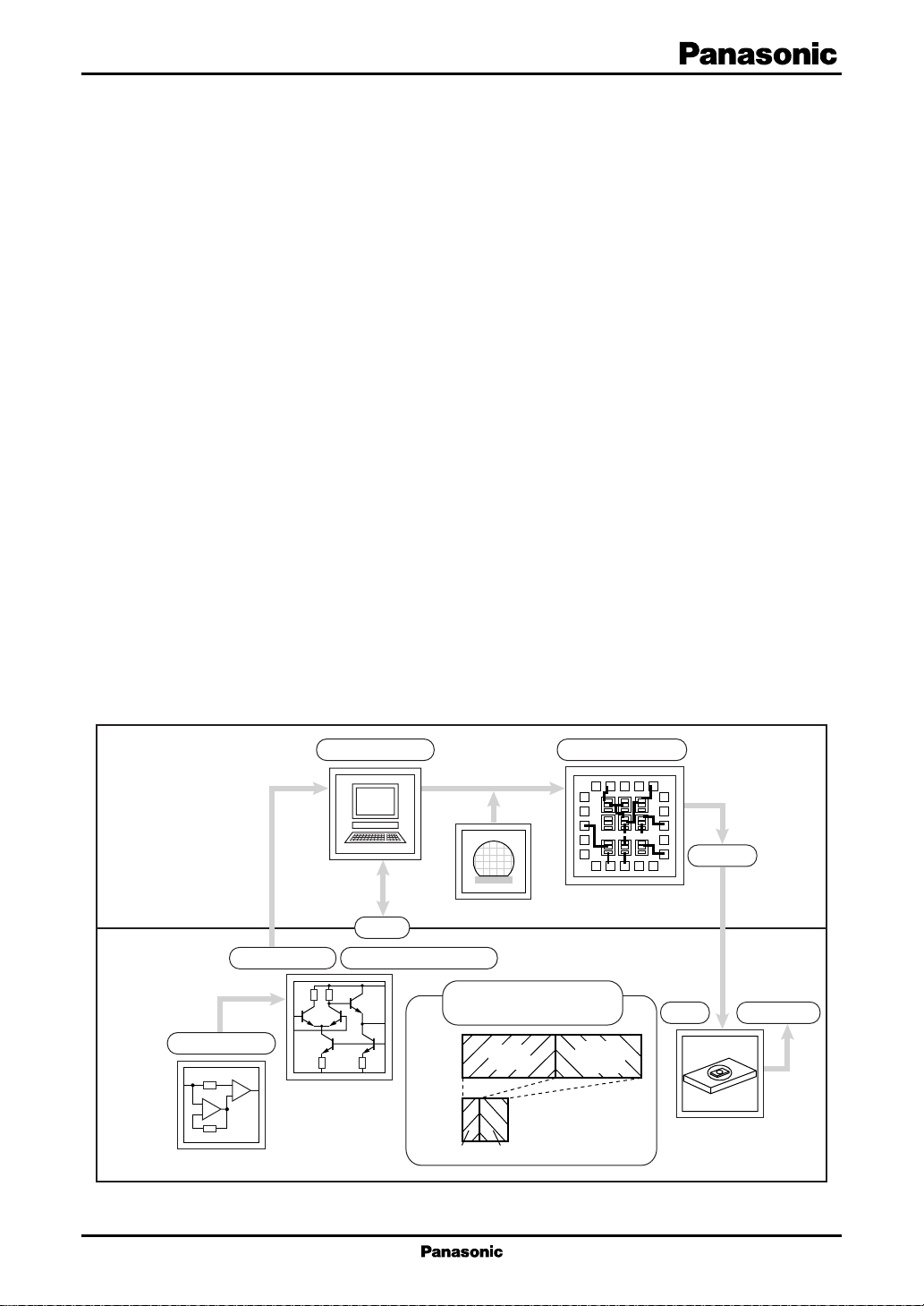
Starting from a wafer on which a most part of IC diffusion processes are already finished, you can shorten an IC pilot
fabrication considerably. Further, placement of elements and inter-element wiring are done automatically by a computer, which results in short period of pattern designing and thereby developing a custom IC in a short period.
■ Features
• High design flexibility
• Easy circuit constant design because of setting resistance or capacitance to an arbitrary value.
• Free setting of contacts between a substrate and GND wiring prevents from operation error to be caused by floating
of substrate potential.
• Usable for multi power source because a resistor island potential can be set for each unit.
• Builds in a lateral type PNP transistor of high reverse breakdown voltage between base and emitter, or a collector
wall type NPN transistor of excellent saturation characteristics. (AN9DA00, AN9DB00, AN9DF00)
• Short development period
• Due to a full automatic layout design, a sample is available in one month from a completion of a circuit diagram.
• Applicable to a small quantity production item
• Possible to develop a custom IC for small quantity production due to a low development cost.
■ Development Flow
Matsushita side
Customer side
System design
Full automatic
layout
Circuit design
Mask layout
EWS
Fabricated wafer
Check
Test specification, etc.
for small quantity production
Full
custom
Master
slice
1week 3weeks
Wiring, assembly
Wired mask only
Drastic shrinkage of TAT
Layout
8weeks
1 000 elements in case
of general-use process
Diffusion,
assembly
6weeks
Selection
Chip Evaluation
1

AN9D, AN9E, AN9F Series Analog Master Slice
■ Product Mix
Series name
Supply
voltage
f
T(max)
AN9D series to 12 V 2.6 GHz 14.4 V 100 to 250 1.0 GHz 14.4 V 66 to 200 For low power dissipation/
AN9E series
to 12 V 3.5 GHz 14.4 V 80 to 250 1.5 GHz 14.4 V 50 to 130 For Bi-CMOS IC
AN9F series to 30 V 300 MHz 30 V 80 to 250 9 MHz 30 V 80 to 350 For high breakdown
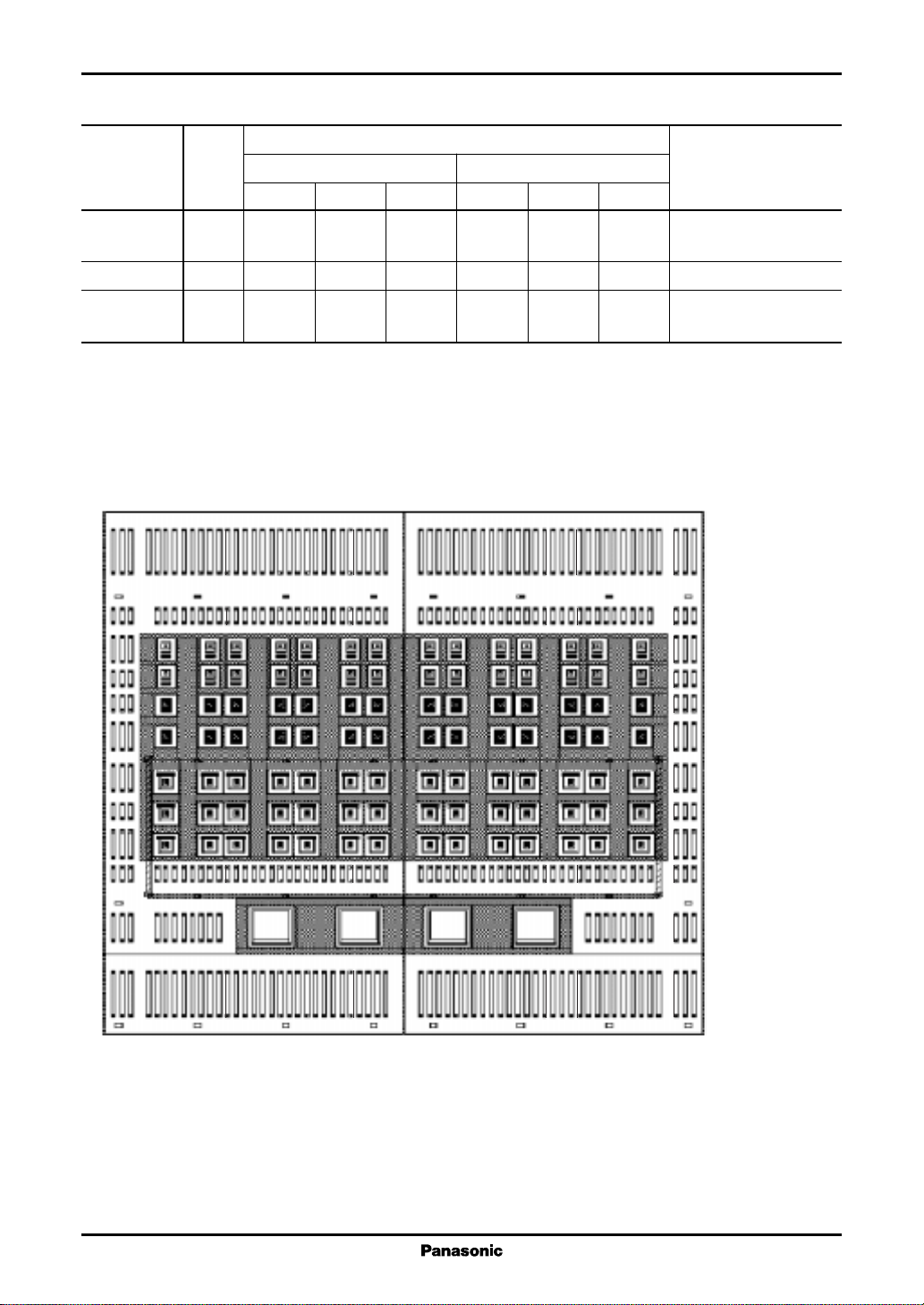
■ Basic Block Configuration (AN9DA00, AN9DB00, AN9DF00)
Element characteristics
NPN transistor PNP transistor Remarks
BV
CEO
h
FE
f
T(max)
BV
CEO
h
FE
high speed operation IC
voltage IC
SP2 resistor
(variable)
SP resistor
(fixed)
PNP transistor
(lateral type)
PNP transistor
(vertical type)
NPN transistor
(collector wall type)
SP resistor
(fixed)
Capacitance
SP2 resistor
(variable)
2
 Loading...