

Panasonic AN8847SB Datasheet
ICs for Compact Disc/CD-ROM Player
AN8847SB
Head amplifier IC for CD-ROM drive (for 32 times speed or more)
■ Overview
The AN8847SB is a head amplifier IC for
digital servo. It can configure an efficient CD-ROM
system in combination with the MN662753, and
allows a full-automatic adjustment of tracking balance-gain-offset and focus balance-gain-offset with
fewer external parts.
Built-in functions are a variable equalizer, high
band RF amp. and AGC which meet CAV playback
with 32 times speed or more.
■ Features
• Variable equalizer which meets CAV playback
with 32 times speed or more.
• Wide band RF amp. and AGC (f
more (−3 dB))
• Balance adjustment function built-in
Focus error amp./tracking error amp.
• CD-RW playback compatible.
Variable gain
Focus error amp./tracking error amp.
(to +16.9 dB)
• OFTR/BDO detection
• APC amp.
= 30 MHz or
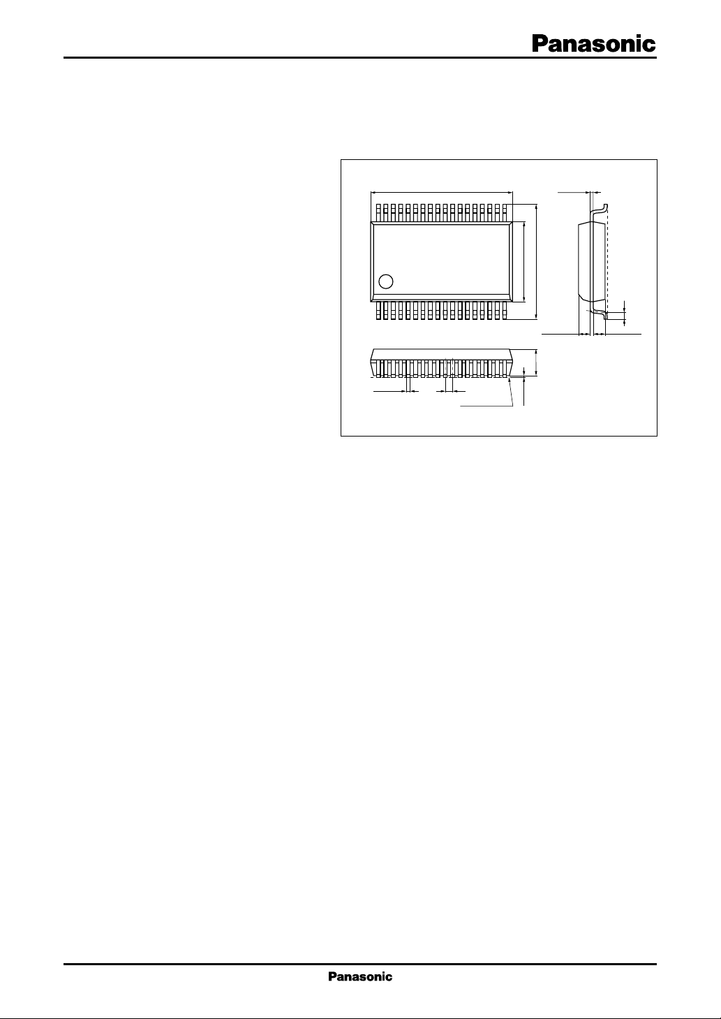
C
Unit: mm
+0.10
36 19
15.2±0.3
118
0.3±0.11 0.8
Seating plane
SSOP036-P-0450A
0.2
–0.05
8.4±0.3
11.93±0.3
1.30±0.25 1.30±0.25
2.85±0.2
0.1±0.1
0.5
■ Applications
• CD/CD-ROM drive
1
AN8847SB ICs for Compact Disc/CD-ROM Player
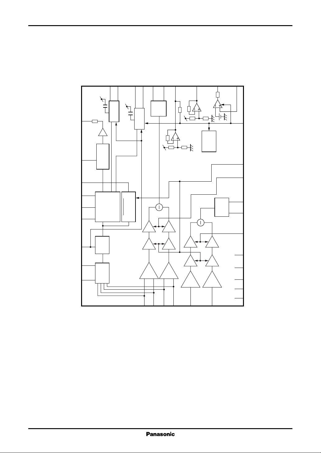
■ Block Diagram
3TOUT
CEA
NRFDET
ARF
CAGC
RFC
EQCTL
RFOUT
RFN
12
11
17
10
9
8
7
6
4
13
ENV
detection
RF AGC
EQ
amp.
ADD
BDO
CBDO
14
BDO
COFTR
15
AC
RFDET
OFTR
16
OFTR
BCA
GCA
ADD
36
26
amp.
35
FEN
Amp.
FEOUT
27
BCA
GCA
ADD
34
22
amp.
33
REF2
V
BCA
GCA
Amp.
32
20
REF1
V
LD
2
Standby
BCA
GCA
Amp.
31
Amp.
1
19
28
29
24
25
30
23
21
18
PD
3
5
LDON
GCTRL
FBAL
TEN
TEOUT
TBAL
V
CC2
V
CC1
GND
RV
CC
RGND
2

ICs for Compact Disc/CD-ROM Player AN8847SB
■ Pin Descriptions
Pin No. Description
1 APC amp. input pin
2 APC amp. output pin
3 Power supply pin (R)
4 RF addition amp. inverted input pin
5 GND pin (R)
6 RF addition amp. output pin
7 EQ characteristics control pin
8
Capacitor connection pin for HPF of AGC input
9 AGC loop filter connection pin
10 AGC output pin
11 Capacitor connection pin for HPF amp.
12 3TENV output pin
13 Capacitor connection pin for RF dark-side
envelope detection
14 BDO output pin
15 Capacitor connection pin for RF right-side
envelope detection
16 OFTR output pin
17 NRFDET output pin
Pin No. Description
18 GND pin
19 APC & standby control pin
20 V
output pin
REF1
21 Power supply pin 1
22 V
output pin
REF2
23 Power supply pin 2
24 TE amp. inverted input pin
25 TE amp. output pin
26 FE amp. inverted input pin
27 FE amp. output pin
28 GCTL pin
29 FBAL control pin
30 TBAL control pin
31 Tracking signal input pin 1
32 Tracking signal input pin 2
33 Focus signal input pin 4
34 Focus signal input pin 2
35 Focus signal input pin 3
36 Focus signal input pin 1
■ Absolute Maximum Ratings
Parameter Symbol Rating Unit
1
*
*
*
*
*
*
1
1
1
1
1
*1, *
V
CCR
V
CC1
V
CC2
I
CCR
I
CC1
I
CC2
2
1
*
1
*
P
D
T
opr
T
stg
5.8 V
5.8 V
5.8 V
97.1 mA
7.4 mA
2.43 mA
403 mW
−20 to +75 °C
−55 to +125 °C
Supply voltage R
Supply voltage 1
Supply voltage 2
Supply current R
Supply current 1
Supply current 2
Power dissipation
Operating ambient temperature
Storage temperature
Note)*1: Except for the power dissipation, operating ambient temperature and storage temperature, all ratings are for Ta = 25°C.
2: The value for the independent package (without a heat sink) at Ta = 75°C.
*
■ Recommended Operating Range
Parameter Symbol Range Unit
Supply voltage R V
Supply voltage 1 V
Supply voltage 2 V
CCR
CC1
CC2
4.5 to 5.5 V
4.5 to 5.5 V
3.0 to 5.5 V
3
 Loading...