

Panasonic AN8816SB Datasheet
ICs for CD/CD-ROM Player
■ Overview
The AN8816SB is a 4ch. driver using the power operational amplifier method. It employs the surface mounting
type package superior in radiation characteristics.
■ Features
•
Wide output D-range is available regardless of refer-
ence voltage on the system
•
Setting of driver input/output gain enabled by external
resistance
•
2ch. independently controllable PC (Power Cut) feature
built-in
•
Thermal shut down circuit (with hysteresis) built-in
•
Proper heat of IC controllable by separating the output
supply and setting each independently for 2ch.
•
Construction of 5V supply enabled by external PNP Tr
•
Accessary operational amplifier built-in
•
Relatively easy pattern design by separating and con-
centrating the input line and output line
■ Application
Actuator for CD/CD-ROM, motor driver
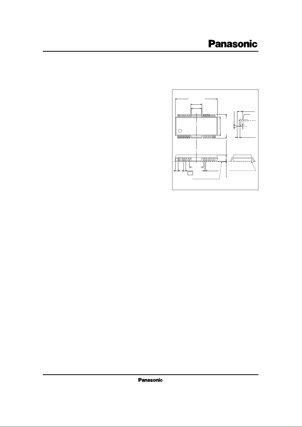
AN8816SB
4ch. Linear Driver IC for CD/CD-ROM
1 14
18.40±0.20
(5.15)
(4.80)
10.93±0.30
8.30±0.20
(6.40)
(1.20) 0.8
0.35
2.70±0.20
0.65±0.20
0 ~10˚
Unit : mm
78
28 1522 21
(1.315)
0.30
+ 0.10
– 0.05
+0.10
– 0.05
0.10±0.10
SEATING PLANE
SEATING PLANE
Fin-attached 28-lead SOP package (HSOP-042-0400)
ICs for CD/CD-ROM Player
AN8816SB
■ Block Diagram
23 25 2719
9111213141516171820
7
Fin
22
2
1
5
6
4
21
PGND1 IN1 IN2 IN3 IN4
SV
CC
PV
CC1
VO1+ VO1– VO2+ VO2– VO3+ VO3– VO4+ VO4– PV
CC2
R
L4
R
L3
R
L2
R
L1
PV
CC
1
2
SV
CC
8
SGND
V
REF
+
–
I
L
PV
CC
1
2
– +
24 26 28 10
PGND2PC1 PC2
5V
reg
Motor or Coil
Direction
Det.
Direction
Det.
Direction
Det.
Direction
Det.
Thermal
Protector
VCC Monitor
V
REF
Monitor
– +– +– +– +– +– +– +– +
– +– +– +– +
ICs for CD/CD-ROM Player
AN8816SB
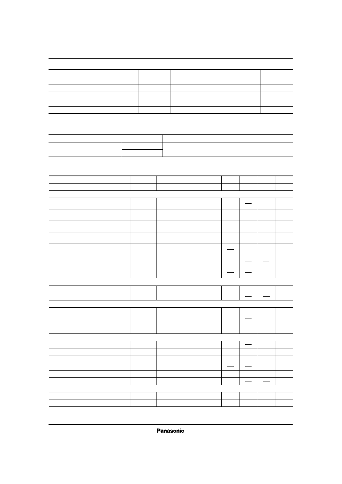
■ Absolute Maximum Ratings (Ta=25˚C)
V
CC
I
CC
P
D
T
opr
T
stg
Supply Voltage
Supply Current
Power Dissipation
Note)
Operating Ambient Temperature
Storage Temperature
V
mA
mW
˚C
˚C
Parameter Symbol Rating Unit
18
3141
–30 ~ + 85
–55 ~ + 150
Note) For surface mounting on 100 × 80 × 1.6 mm double face glass epoxy board.
■ Recommended Operating Range (Ta=25˚C)
5.5V ~ 14V
Parameter Symbol Range
Operating Supply Voltage Range
SV
CC
Note)
PV
CC1
, PV
CC2
Note) Set SV
CC
to the maximum electric potential.
■ Electrical Characteristics (Ta=25˚C)
Parameter Symbol Condition min. typ. max. Unit
Drivers 1 to 4
Input Offset Voltage
Output Offset Voltage
Gain
Maximum Output Amplitude (+)
Maximum Output Amplitude (–)
Threshold H
Threshold L
V
IOF
V
OOF
G
V
L+
V
L–
V
PCH
V
PCL
mV
mV
dB
V
V
V
V
5
–50
15
5
500
1.7
( )
( )
20
5.0
–5.0
Total Circuit Current
I
tot
PV
CC1
= PV
CC2
= SV
CC
= 8V
PV
CC1
= PV
CC2
= SV
CC
= 8V
R
L
= 8Ω, R
IN
= 10kΩ
3.0
2.0
10
mA
3.3
–10
–50
18
4.4
2.0
10
50
22
–4.4
0.3
Reset Circuit
Reset Operation Release Supply Voltage
V
REF
Detection
5V Regulator
Output Voltage
Output Load Fluctuation
Supply Voltage Fluctuation
V
RST
V
REF
3.2 V
V
I
IN
= 10µA, R
IN
= 10kΩ
4.75 5.25
50
5
V
REG
DV
R
DV
V
5.0
V
mV
mV
PV
CC1
= PV
CC2
= SV
CC
= 8V
PV
CC1
= PV
CC2
= SV
CC
= 8V
PV
CC1
= PV
CC2
= SV
CC
= 8V~12V
–5
100
–5
6.0
2.0
2.0
( )
( )
mV
nA
V
V
mA
mA
OP Amp.
Input Offset Voltage
Input Bias Current
High Level Output Voltage
Low Level Output Voltage
Output Drive Current Sink
Output Drive Current Source
V
OF
I
BOP
V
OH
V
OL
I
SIN
I
SOU
PV
CC1
= PV
CC2
= SV
CC
= 8V
PV
CC1
= PV
CC2
= SV
CC
= 8V
PV
CC1
= PV
CC2
= SV
CC
= 8V
PV
CC1
= PV
CC2
= SV
CC
= 8V
PV
CC1
= PV
CC2
= SV
CC
= 8V
PV
CC1
= PV
CC2
= SV
CC
= 8V
Heat Protection Circuit
Operation Temperature Equilibrium Value
Note 1)
Operation Temperature Hysteresis Width
Note 1)
T
THD
DT
THD
(180)
(45)
˚C
˚C
PV
CC1
= PV
CC2
= SV
CC
= 8V
R
L
= 8Ω, R
IN
= 10kΩ
PV
CC1
= PV
CC2
= SV
CC
= 8V
R
L
= 8Ω, R
IN
= 10kΩ
PV
CC1
= PV
CC2
= SV
CC
= 8V
R
L
= 8Ω, R
IN
= 10kΩ
PV
CC1
= PV
CC2
= SV
CC
= 8V
R
L
= 8Ω, R
IN
= 10kΩ
PV
CC1
= PV
CC2
= SV
CC
= 8V
R
L
= 8Ω, R
IN
= 10kΩ
PV
CC1
= PV
CC2
= SV
CC
= 8V
R
L
= 8Ω, R
IN
= 10kΩ
Note 1) Characteristic value in parentheses is a reference value for design but not a guaranteed value.
 Loading...